EP0370428A2 - Process for manufacturing gate electrodes - Google Patents
Process for manufacturing gate electrodes Download PDFInfo
- Publication number
- EP0370428A2 EP0370428A2 EP89121433A EP89121433A EP0370428A2 EP 0370428 A2 EP0370428 A2 EP 0370428A2 EP 89121433 A EP89121433 A EP 89121433A EP 89121433 A EP89121433 A EP 89121433A EP 0370428 A2 EP0370428 A2 EP 0370428A2
- Authority
- EP
- European Patent Office
- Prior art keywords
- layer
- structuring
- polymer layer
- polymer
- mushroom
- Prior art date
- Legal status (The legal status is an assumption and is not a legal conclusion. Google has not performed a legal analysis and makes no representation as to the accuracy of the status listed.)
- Granted
Links
- 238000000034 method Methods 0.000 title claims abstract description 44
- 230000008569 process Effects 0.000 title claims abstract description 23
- 238000004519 manufacturing process Methods 0.000 title claims abstract description 8
- 230000005669 field effect Effects 0.000 claims abstract description 4
- 229920002120 photoresistant polymer Polymers 0.000 claims abstract 2
- 229920000642 polymer Polymers 0.000 claims description 50
- 238000005530 etching Methods 0.000 claims description 46
- 239000002184 metal Substances 0.000 claims description 7
- 229910052751 metal Inorganic materials 0.000 claims description 7
- VYPSYNLAJGMNEJ-UHFFFAOYSA-N Silicium dioxide Chemical compound O=[Si]=O VYPSYNLAJGMNEJ-UHFFFAOYSA-N 0.000 claims description 6
- 239000000758 substrate Substances 0.000 claims description 6
- 238000001312 dry etching Methods 0.000 claims description 4
- 239000000463 material Substances 0.000 claims description 4
- 229910052581 Si3N4 Inorganic materials 0.000 claims description 3
- 229910052681 coesite Inorganic materials 0.000 claims description 3
- 229910052906 cristobalite Inorganic materials 0.000 claims description 3
- 239000000377 silicon dioxide Substances 0.000 claims description 3
- 235000012239 silicon dioxide Nutrition 0.000 claims description 3
- 229910052682 stishovite Inorganic materials 0.000 claims description 3
- 229910052905 tridymite Inorganic materials 0.000 claims description 3
- 238000000151 deposition Methods 0.000 claims 1
- 229910052732 germanium Inorganic materials 0.000 claims 1
- GNPVGFCGXDBREM-UHFFFAOYSA-N germanium atom Chemical compound [Ge] GNPVGFCGXDBREM-UHFFFAOYSA-N 0.000 claims 1
- 238000001020 plasma etching Methods 0.000 description 4
- 230000001976 improved effect Effects 0.000 description 2
- 239000012212 insulator Substances 0.000 description 2
- 150000002500 ions Chemical class 0.000 description 2
- 239000000126 substance Substances 0.000 description 2
- 235000001674 Agaricus brunnescens Nutrition 0.000 description 1
- 229910001218 Gallium arsenide Inorganic materials 0.000 description 1
- 230000008901 benefit Effects 0.000 description 1
- 238000010894 electron beam technology Methods 0.000 description 1
- 238000009413 insulation Methods 0.000 description 1
- 230000003287 optical effect Effects 0.000 description 1
- 238000000206 photolithography Methods 0.000 description 1
- 229920003229 poly(methyl methacrylate) Polymers 0.000 description 1
- 239000004926 polymethyl methacrylate Substances 0.000 description 1
- 238000002360 preparation method Methods 0.000 description 1
- 239000004065 semiconductor Substances 0.000 description 1
- 238000004381 surface treatment Methods 0.000 description 1
- 238000012546 transfer Methods 0.000 description 1
- 238000007740 vapor deposition Methods 0.000 description 1
Images


Classifications
-
- H—ELECTRICITY
- H01—ELECTRIC ELEMENTS
- H01L—SEMICONDUCTOR DEVICES NOT COVERED BY CLASS H10
- H01L29/00—Semiconductor devices adapted for rectifying, amplifying, oscillating or switching, or capacitors or resistors with at least one potential-jump barrier or surface barrier, e.g. PN junction depletion layer or carrier concentration layer; Details of semiconductor bodies or of electrodes thereof ; Multistep manufacturing processes therefor
- H01L29/66—Types of semiconductor device ; Multistep manufacturing processes therefor
- H01L29/66007—Multistep manufacturing processes
- H01L29/66075—Multistep manufacturing processes of devices having semiconductor bodies comprising group 14 or group 13/15 materials
- H01L29/66227—Multistep manufacturing processes of devices having semiconductor bodies comprising group 14 or group 13/15 materials the devices being controllable only by the electric current supplied or the electric potential applied, to an electrode which does not carry the current to be rectified, amplified or switched, e.g. three-terminal devices
- H01L29/66409—Unipolar field-effect transistors
- H01L29/66848—Unipolar field-effect transistors with a Schottky gate, i.e. MESFET
- H01L29/66856—Unipolar field-effect transistors with a Schottky gate, i.e. MESFET with an active layer made of a group 13/15 material
- H01L29/66863—Lateral single gate transistors
-
- H—ELECTRICITY
- H01—ELECTRIC ELEMENTS
- H01L—SEMICONDUCTOR DEVICES NOT COVERED BY CLASS H10
- H01L21/00—Processes or apparatus adapted for the manufacture or treatment of semiconductor or solid state devices or of parts thereof
- H01L21/02—Manufacture or treatment of semiconductor devices or of parts thereof
- H01L21/04—Manufacture or treatment of semiconductor devices or of parts thereof the devices having at least one potential-jump barrier or surface barrier, e.g. PN junction, depletion layer or carrier concentration layer
- H01L21/18—Manufacture or treatment of semiconductor devices or of parts thereof the devices having at least one potential-jump barrier or surface barrier, e.g. PN junction, depletion layer or carrier concentration layer the devices having semiconductor bodies comprising elements of Group IV of the Periodic System or AIIIBV compounds with or without impurities, e.g. doping materials
- H01L21/28—Manufacture of electrodes on semiconductor bodies using processes or apparatus not provided for in groups H01L21/20 - H01L21/268
- H01L21/283—Deposition of conductive or insulating materials for electrodes conducting electric current
- H01L21/285—Deposition of conductive or insulating materials for electrodes conducting electric current from a gas or vapour, e.g. condensation
- H01L21/28506—Deposition of conductive or insulating materials for electrodes conducting electric current from a gas or vapour, e.g. condensation of conductive layers
- H01L21/28575—Deposition of conductive or insulating materials for electrodes conducting electric current from a gas or vapour, e.g. condensation of conductive layers on semiconductor bodies comprising AIIIBV compounds
- H01L21/28587—Deposition of conductive or insulating materials for electrodes conducting electric current from a gas or vapour, e.g. condensation of conductive layers on semiconductor bodies comprising AIIIBV compounds characterised by the sectional shape, e.g. T, inverted T
Definitions
- the invention relates to a method for producing gate electrodes according to the preamble of patent claim 1.
- the invention has for its object to provide a method in which the cross-sectional dimensions of the gate electrode are variably adjustable and the transistor properties can thereby be improved.
- the method has the advantage that all etching steps for producing the gate structure can be carried out on a dry etching system.
- the method is easily reproducible and different cross sections of the gate electrode can be produced in a labor-economical manner.
- the generation of gate structures with a very short gate length, which have a low lead resistance of the gate electrode are advantageous for the production of high-frequency field effect transistors. This leads to an increase in the maximum cut-off frequency and better amplifier properties of the transistor.
- the noise behavior of the transistor is improved.
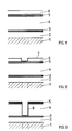
- FIGS. 1 to 14 show the process sequence, including some process variants for producing a gate electrode which is mushroom-shaped in cross section.
- a mushroom-shaped gate electrode with a small footprint and an extensive overhang is produced by means of the method described below.
- the invention uses a 5-layer technique, the structure of which is shown in FIG. 1.
- a semiconductor substrate e.g. GaAs
- an approximately 200 to 500 nm thick first polymer layer e.g. Photoresist AZ4040, applied.
- a thin structuring layer 3 e.g. SiO2, Si3N4 or Ge from about 10 to 50 and then a thick second polymer layer 4, e.g. Photoresist AZ 4110 from about 500 to 1100nm deposited.
- This top layer 6 consists either of a photoresist for optical lithography, e.g. Photoresist AZ4040, or from an electron sensitive photoresist for electron optical exposure, e.g. PMMA, to achieve the finest structures.
- the invention uses etching processes, e.g. Plasma etching.
- the individual etching processes must have the highest possible selectivity between the polymer layers 2, 4, 6 and the structuring layers 3, 5.
- the base structure 7 of the gate contact is produced lithographically in the top polymer layer (FIG. 2).
- the base structure 7 is then introduced into the upper structuring layer 5 via a dry etching step and then this structure is transferred exactly to the lower structuring layer 3 by means of anisotropic RIE (reactive ion etching) etching.
- the upper polymer layer 6 is removed and the trench 8 is formed perpendicular to the layers 4, 5 (FIG. 3).
- a The following isotropic dry etching step produces an underetching of the upper structuring layer 5 and the trench 9 (FIG. 4) expanded downward is formed in the second polymer layer 4.
- a window in the lower structuring layer 3 is opened and a subsequent anisotropic RIE etching process transfers the base structure down to the substrate surface.
- the mushroom-shaped trench 10 is formed (FIG. 5).
- the overhang 11 of the upper structuring layer 5 serves as an etching mask, since in this etching step it is mainly the reactive ions directed vertically onto the surface that cause the etching.
- the window in the lower structuring layer 3 is opened, the upper structuring layer 5 is removed with the same material from the upper and lower structuring layer.
- the upper structuring layer 5 must therefore be chosen thicker than the lower structuring layer.
- the desired structure 12 is produced (FIG. 6).
- the oblique side walls of the second polymer layer 4 of the mushroom-shaped trench 10 are not covered with gate metal (FIG. 7).
- a subsequent lift-off process of the second polymer layer 4 simultaneously removes the unwanted metal layer 14 above the second polymer layer 4.
- the lower structuring layer 3 and the first polymer layer 2 are etched away or detached and the mushroom-shaped gate electrode 13 has a foot 15 with the original base structure 7 and a wide head 16 (Fig. 8).
- the layer thicknesses of the structuring layers are chosen so thin that there is sufficient transparency of the layers for adjustment purposes in the case of electron beam exposure.
Abstract
Description
Die Erfindung betrifft ein Verfahren zur Herstellung von Gate-Elektroden nach dem Oberbegriff des Patentanspruchs 1.The invention relates to a method for producing gate electrodes according to the preamble of
Das Verfahren findet Verwendung bei der Herstellung von Hochfrequenz-Feldeffekttransistoren.
Aus eine Veröffentlichung von P.C.Chao et al. in IEEE Trans. Electr. Dev., Vol. ED-32, 1042 (1985) ist ein Verfahren zur Herstellung von T-förmigen Gate-Elektroden bekannt, bei dem drei Fotolackschichten zum Aufbau einer entsprechenden Gate-Struktur verwendet werden.The method is used in the production of high-frequency field-effect transistors.
From a publication by PCChao et al. in IEEE Trans. Electr. Dev., Vol. ED-32, 1042 (1985) discloses a method for producing T-shaped gate electrodes, in which three photoresist layers are used to build up a corresponding gate structure.
Der Erfindung liegt die Aufgabe zugrunde, ein Verfahren anzugeben, bei dem die Querschnittsdimensionen der Gate-Elektrode variabel einstellbar sind und dadurch die Transistoreigenschaften verbessert werden können.The invention has for its object to provide a method in which the cross-sectional dimensions of the gate electrode are variably adjustable and the transistor properties can thereby be improved.
Das Verfahren hat den Vorteil, daß alle Ätzschritte zur Herstellung der Gate-Struktur auf einer Trockenätzanlage durchgeführt werden können. Das Verfahren ist gut reproduzierbar und es lassen sich in arbeitsökonomischer Weise unterschiedliche Querschnitte der Gate-Elektrode erzeugen. Insbesondere die Erzeugung von Gate-Strukturen mit einer sehr kurzen Gate-Länge, die einen geringen Zuleitungswiderstand der Gate-Elektrode besitzen, sind für die Herstellung von hochfrequenten Feldeffekttransistoren von Vorteil. Dadurch erreicht man eine Erhöhung der maximalen Grenzfrequenz und bessere Verstärkereigenschaften des Transistors. Außerdem wird das Rauschverhalten des Transistors verbessert.The method has the advantage that all etching steps for producing the gate structure can be carried out on a dry etching system. The method is easily reproducible and different cross sections of the gate electrode can be produced in a labor-economical manner. In particular, the generation of gate structures with a very short gate length, which have a low lead resistance of the gate electrode, are advantageous for the production of high-frequency field effect transistors. This leads to an increase in the maximum cut-off frequency and better amplifier properties of the transistor. In addition, the noise behavior of the transistor is improved.
Die Erfindung wird im folgenden anhand eines Ausführungsbeispiels näher erläutert unter Bezugnahme auf schematische Zeichnungen.The invention is explained in more detail below using an exemplary embodiment with reference to schematic drawings.
In den Figuren 1 bis 14 ist der Verfahrensablauf einschließlich einiger Verfahrensvarianten zur Herstellung einer im Querschnitt pilzförmigen Gate-Elektrode dargestellt.FIGS. 1 to 14 show the process sequence, including some process variants for producing a gate electrode which is mushroom-shaped in cross section.
Erfindungsgemäß wird vermittels des nachstehend beschriebenen Verfahrens eine im Querschnitt pilzförmige Gate-Elektrode also mit kleiner Standfläche und ausgedehntem Überhang hergestellt.According to the invention, a mushroom-shaped gate electrode with a small footprint and an extensive overhang is produced by means of the method described below.
Die Erfindung benutzt eine 5-Lagen-Technik, deren Aufbau in Fig. 1 dargestellt ist. Auf einem Halbleitersubstrat 1, z.B. GaAs, wird eine etwa 200 bis 500nm dicke erste Polymerschicht 2, z.B. Fotolack AZ4040, aufgebracht. Darüber wird eine dünne Strukturierungsschicht 3, z.B. SiO₂, Si₃N₄ oder Ge von ca. 10 bis 50 und danach eine dicke zweite Polymerschicht 4, z.B. Fotolack AZ 4110 von etwa 500 bis 1100nm abgeschieden. Darüber wird eine weitere Strukturierungsschicht 5, z.B. SiO₂, Si₃N₄ oder He mit ca. 30 bis 150nm und zuletzt eine dünne oberste Polymerschicht mit ca. 50 bis 300nm aufgebracht. Diese oberste Schicht 6 besteht entweder aus einem Fotolack für die optische Lithografie, z.B. Fotolack AZ4040, oder aus einem elektronenempfindlichen Fotolack für elektronenoptische Belichtung, z.B. PMMA, zur Erzielung feinster Strukturen. Die Erfindung benutzt zur Erzeugung der Tiefenprofile Ätzverfahren, z.B. Plasmaätzen. Zur exakten Übertragung der Dimension der Strukturen der obersten Schicht in die erste Polymerschicht müssen die einzelnen Ätzprozesse eine möglichst hohe Selektivität zwischen den Polymerschichten 2, 4, 6 und den Strukturierungsschichten 3, 5 aufweisen.The invention uses a 5-layer technique, the structure of which is shown in FIG. 1. On a
Zunächst wird lithografisch in der obersten Polymerschicht die Sockelstruktur 7 des Gatekontaktes hergestellt (Fig. 2). Danach wird über einen Trockenätzschritt die Sockelstruktur 7 in die obere Strukturierungsschicht 5 eingebracht und anschließend mittels anisotropen RIE (reactive ion etching)-Ätzen diese Struktur exakt bis zur unteren Strukturierungsschicht 3 übertragen. Die obere Polymerschicht 6 wird dabei entfernt und es entsteht der Graben 8 senkrecht zu den Schichten 4, 5 (Fig. 3). Ein folgender isotroper Trockenätzschritt erzeugt eine Unterätzung der oberen Strukturierungsschicht 5 und est entsteht der nach unten erweiterte Graben 9 (Fig. 4) in der zweiten Polymerschicht 4. Anschließend wird ein Fenster in der unteren Strukturierungsschicht 3 geöffnet und ein folgender anisotroper RIE-Ätzprozeß überträgt die Sockelstruktur bis auf die Substratoberfläche. Es entsteht der pilzförmige Graben 10 (Fig. 5). Der Überhang 11 der oberen Strukturierungsschicht 5 dient dabei als Ätzmaske, da bei diesem Ätzschritt hauptsächlich die vertikal auf die Oberfläche gerichteten reaktiven Ionen die Ätzung bewirken. Beim öffnen des Fensters in der unteren Strukturierungsschicht 3 wird bei gleichem Material von oberer und unterer Strukturierungsschicht die obere Strukturierungsschicht 5 mit abgetragen. Deshalb muß die obere Strukturierungsschicht 5 dicker gewählt werden als die untere Strukturierungsschicht. Nach dem Abätzen der oberen Strukturierungsschicht 5 ist die gewünschte Struktur 12 erzeugt (Fig. 6). Beim anschließenden Aufdampfen des Gate-Metalls belegen sich die schrägen Seitenwände der zweiten Polymerschicht 4 des pilzförmigen Grabens 10 nicht mit Gatemetall (Fig. 7). Ein anschließender lift-off-Prozeß der zweiten Polymerschicht 4 beseitigt gleichzeitig die unerwünschte Metallschicht 14 über der zweiten Polymerschicht 4. Danach werden die untere Strukturierungsschicht 3 und die erste Polymerschicht 2 weggeätzt oder abgelöst und die pilzförmige Gate-Elektrode 13 hat einen Fuß 15 mit der ursprünglichen Sockelstruktur 7 und einen breiten Kopf 16 (Fig. 8). Die Schichtdicken der Strukturierungsschichten sind so dünn gewählt, daß eine genügende Transparenz der Schichten für Justierzwecke bei Elektronenstrahlbelichtung gegeben ist.First, the
In Anlehnung an das oben angegebene Verfahren werden nachstehend einige Verfahrensvarianten aufgeführt:
- a) Durch unterschiedliche Materialien der beiden
Strukturierungsschichten Strukturierungsschichten Strukturierungsschicht 5. - b) Als Ätzmaske beim anisotropen Ätzen der
ersten Polymerschicht 2 wird dieobere Strukturierungsschicht 5 benutzt. Infolgedessen muß derÜberhang 11 genügend mechanische und chemische Stabilität aufweisen, und dieobere Strukturierungsschicht 5 muß eine Mindestschichtdicke besitzen. Um diesen Nachteil zu umgehen, wird vor dem isotropen Ätzen derzweiten Polymerschicht 4 einFenster 17 in derunteren Strukturierungsschicht 3 bis zur halben Schichtdicke geöffnet (Fig. 9), und danach erst deraufgeweitete Graben 18 erzeugt (Fig. 10). Das anschließende vollständige Öffnen des Fensters in derunteren Strukturierungsschicht 3 erzeugt eineStufe 19 in dieser Schicht (Fig.11). Es entsteht eine entsprechend derSockelstruktur 7 dimensionierte Öffnung, die für den nachfolgenden anisotropen Ätzprozeß derersten Polymerschicht 2 als Ätzfenster dient. Derverbleibende Randstreifen 20 derunteren Strukturierungsschicht 3 auf derersten Polymerschicht 2 kann sehr dünn sein, da er mechanisch nicht beansprucht wird. Allerdings erfordert diese Verfahrensvariante eine gute Gleichmäßigkeit der Ätzung derStrukturierungsschicht 3. - c) Eine andere Verfahrensvariante benutzt ebenfalls die
untere Strukturierungsschicht 3 als Ätzmaske für das anisotrope Ätzen derersten Polymerschicht 2. Es wird im Gegensatz zur Ausführung nach b) vor dem isotropen Ätzen derzweiten Polymerschicht 4 das Fenster in derunteren Strukturierungsschicht 3 vollkommen geöffnet, danach erst wird das isotrope Ätzen derzweiten Polymerschicht 4 durchgeführt. Dies erfordert jedoch ein selektives Ätzverhalten bei isotropen Ätzbedingungen derzweiten Polymerschicht 4 zurersten Polymerschicht 2. Im einfachsten Falle ist dieerste Polymerschicht 2 ätzresistenter. Anderenfalls muß die Oberfläche derersten Polymerschicht 2 bei der Schichtenpräparation durch geeignete Oberflächenbehandlung chemisch verändert werden, so daß sich eine hohe Ätzresistenz beim isotropen Ätzen ergibt, oder man erzeugt einen ätzresistenten Film (z.B. im Plasma) auf der Oberfläche derersten Polymerschicht 2. Beim anschließenden anisotropen Ätzen mit energiereichen reaktiven Ionen muß dieerste Polymerschicht 2 ätzbar sein. - d) Weist die zweite Polymerschicht (4) eine wesentlich höhere Ätzrate als die
erste Polymerschicht 2 auf, so kann dieuntere Strukturierungsschicht 3 entfallen (4-Lagen-Aufbau). Als Ätzmaske für das anisotrope Ätzen derersten Polymerschicht 2 dient hier die obere Strukturierungsschicht. - e) In Anlehnung an die Verfahrensvariante c) wird die
erste Polymerschicht 2 durch eine anorganische Schicht (z.B. Isolator, Metall) ersetzt und dadurch ein unterschiedliches Ätzverhalten zurzweiten Polymerschicht 4 erzeugt. Die anorganische Schicht muß eine hohe Selektivität zurunteren Strukturierungsschicht 3 besitzen. Die anorganische Schicht wird durch anisotropes Ätzen geätzt.
Bei einem derartigen Schichtaufbau kann dieuntere Zwischenschicht 3 entfallen (4-Lagen-Aufbau). In diesem Fall wird entweder dieobere Zwischenschicht 5 als Ätzmaske für dieanorganische Schicht 2a verwendet oder es wird eineStufe 21 in dieanorganische Schicht 2a vor dem isotropen Ätzen derPolymerschicht 4 durch einen anisotropen Ätzprozeß eingebracht (Fig. 12). Nach dem isotropen Ätzen derPolymerschicht 4 zur Erzeugung des aufgeweiteten Grabens 22 (Fig. 13) wird durch nachfolgendes anisotropes Ätzen deranorganischen Schicht 2a eine Pilzstruktur mit einemabgestuften Fuß 23 erhalten (Fig.14). Die Stufe des Fußes wird dabei je nach mechanischer und chemischer Stabilität desÜberhangs 27 derStrukturierungsschicht 5 unterschiedlich breit ausgebildet. - f) In Anlehnung an die Verfahrensvariante c) wird vor dem Aufweiten der
zweiten Polymerschicht 4 ein Fenster in derunteren Strukturierungsschicht 3 geöffnet. Zum Schutze derersten Polymerschicht 2 wird jedoch vor dem isotropen Ätzen derzweiten Polymerschicht 4 ein dünner Metall- oder Isolatorfilm auf dem Fenster abgeschieden. Im Gegensatz zur Variante nach b) entfällt hier die Erzeugung einer Stufe in der unteren Strukturierungsschicht 3. Die Schichtdicke der unteren Strukturierungsschicht 3 kann somit dünn gewählt werden. Nach dem isotropen Ätzprozeß zur Erzeugung des aufgeweiteten Grabens in der zweiten Poly merschicht 4 wird die Fensterisolierung abgeätzt und das anisotrope Ätzen der ersten unteren Polymerschicht 2 mit der unteren Strukturierungsschicht 3 als Ätzmaske wird anschließend durchgeführt.
- a) Due to different materials of the two
structuring layers structuring layer 5 in the case of very fine gate structures (e.g. for the submicron range). - b) The
upper structuring layer 5 is used as the etching mask during the anisotropic etching of thefirst polymer layer 2. As a result, theoverhang 11 must have sufficient mechanical and chemical stability, and theupper structuring layer 5 must have a minimum layer thickness. To avoid this disadvantage, awindow 17 in thelower structuring layer 3 is opened up to half the layer thickness before the isotropic etching of the second polymer layer 4 (FIG. 9), and only then is the widenedtrench 18 produced (FIG. 10). The subsequent complete opening of the window in thelower structuring layer 3 creates astep 19 in this layer (FIG. 11). An opening corresponding to thebase structure 7 is created, which serves as an etching window for the subsequent anisotropic etching process of thefirst polymer layer 2. The remainingedge strip 20 of thelower structuring layer 3 on thefirst polymer layer 2 can be very thin, since it is not mechanically stressed. However, this process variant requires one good uniformity of the etching of thestructuring layer 3. - c) Another process variant also uses the
lower structuring layer 3 as an etching mask for the anisotropic etching of thefirst polymer layer 2. In contrast to the embodiment according to b), the window in thelower structuring layer 3 is completely opened before the isotropic etching of thesecond polymer layer 4, then only the isotropic etching of thesecond polymer layer 4 is carried out. However, this requires a selective etching behavior under isotropic etching conditions of thesecond polymer layer 4 to thefirst polymer layer 2. In the simplest case, thefirst polymer layer 2 is more resistant to etching. Otherwise, the surface of thefirst polymer layer 2 must be chemically changed in the layer preparation by means of suitable surface treatment, so that a high etching resistance is obtained during isotropic etching, or an etching-resistant film (for example in plasma) is produced on the surface of thefirst polymer layer 2 anisotropic etching with high-energy reactive ions, thefirst polymer layer 2 must be etchable. - d) If the second polymer layer (4) has a significantly higher etching rate than the
first polymer layer 2, then thelower structuring layer 3 can be omitted (4-layer structure). The upper structuring layer serves as the etching mask for the anisotropic etching of thefirst polymer layer 2. - e) Based on process variant c), the
first polymer layer 2 is covered by an inorganic layer (eg Insulator, metal) and thereby produces a different etching behavior to thesecond polymer layer 4. The inorganic layer must have a high selectivity for thelower structuring layer 3. The inorganic layer is etched by anisotropic etching.
With such a layer structure, the lowerintermediate layer 3 can be dispensed with (4-layer structure). In this case, either the upperintermediate layer 5 is used as an etching mask for theinorganic layer 2a or astep 21 is introduced into theinorganic layer 2a before the isotropic etching of thepolymer layer 4 by an anisotropic etching process (FIG. 12). After the isotropic etching of thepolymer layer 4 to produce the widened trench 22 (FIG. 13), a subsequent mushroom structure with a steppedfoot 23 is obtained by subsequent anisotropic etching of theinorganic layer 2a (FIG. 14). The step of the foot is formed with different widths depending on the mechanical and chemical stability of theoverhang 27 of thestructuring layer 5. - f) Based on the process variant c), a window in the
lower structuring layer 3 is opened before thesecond polymer layer 4 is expanded. To protect thefirst polymer layer 2, however, a thin metal or insulator film is deposited on the window before the isotropic etching of thesecond polymer layer 4. In contrast to the variant according to b), the generation of a step in thelower structuring layer 3 is omitted here. The layer thickness of thelower structuring layer 3 can thus be chosen to be thin. After the isotropic etching process to produce the widened trench in thesecond poly Layer 4, the window insulation is etched off and the anisotropic etching of the firstlower polymer layer 2 with thelower structuring layer 3 as an etching mask is then carried out.
Claims (13)
- daß die in der oberen Polymerschicht (6) vorgegebene Sockelstruktur der Gate-Elektrode (7) durch einen Trockenätzprozeß in die obere Strukturierungsschicht (5) und anschließend durch einen anisotropen Ätzprozeß auf die erste Strukturierungsschicht (3) übertragen wird, und
- daß die obere Polymerschicht (6) entfernt wird.3. The method according to claims 1 and 2, characterized in
- That in the upper polymer layer (6) predetermined base structure of the gate electrode (7) by a dry etching process in the upper structuring layer (5) and then by an anisotropic etching process is transferred to the first structuring layer (3), and
- That the upper polymer layer (6) is removed.
- daß in der unteren Strukturierungsschicht (3) ein Fenster entsprechend dem Fenster in der oberen Strukturierungsschicht geöffnet wird und durch einen RIE-Ätzprozeß die Sockelstruktur (7) der Gate-Elektrode bis auf die Substratoberfläche übertragen wird , und
- daß die obere Strukturierungsschicht (5) und im erweiterten Graben (9) die untere Strukturierungsschicht (3) entfernt wird und eine im Querschnitt pilzförmige Struktur (12) in der Schichtenfolge entsteht (Fig. 5 und 6).5. The method according to any one of the preceding claims, characterized in
- That in the lower structuring layer (3) a window corresponding to the window in the upper structuring layer is opened and the base structure (7) of the gate electrode is transferred to the substrate surface by an RIE etching process, and
- That the upper structuring layer (5) and in the expanded trench (9), the lower structuring layer (3) is removed and a mushroom-shaped structure (12) is formed in the layer sequence (Fig. 5 and 6).
- daß durch ganzflächiges Abscheiden einer Metallschicht (14) auf der zweiten Polymerschicht (4) und in der pilzförmigen Struktur (12) eine pilzförmiges Gate-Elektrode (13) gebildet wird,
- daß durch ein lift-off-Prozeß die zweite Polymerschicht (4) und gleichzeitig die darauf augebracht Metallschicht (14) entfernt werden, und
- daß anschließend die untere Strukturierungsschicht (3) und die erste Polymerschicht (2) weggätzt werden und lediglich die Gate-Elektrode (13) auf dem Substrat (1) bestehen bleibt (Fig. 8).6. The method according to any one of the preceding claims, characterized in that
- That a mushroom-shaped gate electrode (13) is formed by depositing a metal layer (14) over the entire surface of the second polymer layer (4) and in the mushroom-shaped structure (12),
- That the second polymer layer (4) and at the same time the metal layer (14) applied to it are removed by a lift-off process, and
- That then the lower structuring layer (3) and the first polymer layer (2) are etched away and only the gate electrode (13) remains on the substrate (1) (Fig. 8).
Applications Claiming Priority (2)
| Application Number | Priority Date | Filing Date | Title |
|---|---|---|---|
| DE3839770A DE3839770A1 (en) | 1988-11-25 | 1988-11-25 | METHOD FOR PRODUCING GATE ELECTRODES |
| DE3839770 | 1988-11-25 |
Publications (3)
| Publication Number | Publication Date |
|---|---|
| EP0370428A2 true EP0370428A2 (en) | 1990-05-30 |
| EP0370428A3 EP0370428A3 (en) | 1990-11-28 |
| EP0370428B1 EP0370428B1 (en) | 1995-01-04 |
Family
ID=6367851
Family Applications (1)
| Application Number | Title | Priority Date | Filing Date |
|---|---|---|---|
| EP89121433A Expired - Lifetime EP0370428B1 (en) | 1988-11-25 | 1989-11-20 | Process for manufacturing gate electrodes |
Country Status (2)
| Country | Link |
|---|---|
| EP (1) | EP0370428B1 (en) |
| DE (2) | DE3839770A1 (en) |
Cited By (5)
| Publication number | Priority date | Publication date | Assignee | Title |
|---|---|---|---|---|
| EP0352736A2 (en) * | 1988-07-28 | 1990-01-31 | Siemens Aktiengesellschaft | Process for producing a resist structure on semiconductor material with reducing width in direction of the semiconductor material |
| US5288654A (en) * | 1990-12-26 | 1994-02-22 | Mitsubishi Denki Kabushiki Kaisha | Method of making a mushroom-shaped gate electrode of semiconductor device |
| US5445979A (en) * | 1993-12-28 | 1995-08-29 | Fujitsu Limited | Method of making field effect compound semiconductor device with eaves electrode |
| US5583063A (en) * | 1993-11-30 | 1996-12-10 | Nec Corporation | Method of forming T-shaped, cross-sectional pattern using two layered masks |
| WO2003096399A1 (en) * | 2002-05-11 | 2003-11-20 | United Monolithic Semiconductors Gmbh | Method for producing a semiconductor component, and semiconductor component produced by the same |
-
1988
- 1988-11-25 DE DE3839770A patent/DE3839770A1/en not_active Withdrawn
-
1989
- 1989-11-20 EP EP89121433A patent/EP0370428B1/en not_active Expired - Lifetime
- 1989-11-20 DE DE58908855T patent/DE58908855D1/en not_active Expired - Fee Related
Non-Patent Citations (2)
| Title |
|---|
| IEEE ELECTRON DEVICE LETTERS, Band EDL-7, Nr. 2, Februar 1986, Seiten 69-70, IEEE, New York, US; H.M. MACKSEY: "GaAs power FET's having the gate recess narrower than the gate" * |
| JOURNAL OF THE ELECTROCHEMICAL SOCIETY, Band 133, Nr. 10, Oktober 1986, Seiten 409-416, Manchester, NH, US; C.E. WEITZEL et al.: "A review of GaAs MESFET gate electrode fabrication technologies" * |
Cited By (8)
| Publication number | Priority date | Publication date | Assignee | Title |
|---|---|---|---|---|
| EP0352736A2 (en) * | 1988-07-28 | 1990-01-31 | Siemens Aktiengesellschaft | Process for producing a resist structure on semiconductor material with reducing width in direction of the semiconductor material |
| EP0352736A3 (en) * | 1988-07-28 | 1991-03-27 | Siemens Aktiengesellschaft | Process for producing a resist structure on semiconductor material with reducing width in direction of the semiconductor material |
| US5288654A (en) * | 1990-12-26 | 1994-02-22 | Mitsubishi Denki Kabushiki Kaisha | Method of making a mushroom-shaped gate electrode of semiconductor device |
| US5583063A (en) * | 1993-11-30 | 1996-12-10 | Nec Corporation | Method of forming T-shaped, cross-sectional pattern using two layered masks |
| US5445979A (en) * | 1993-12-28 | 1995-08-29 | Fujitsu Limited | Method of making field effect compound semiconductor device with eaves electrode |
| WO2003096399A1 (en) * | 2002-05-11 | 2003-11-20 | United Monolithic Semiconductors Gmbh | Method for producing a semiconductor component, and semiconductor component produced by the same |
| US7041541B2 (en) | 2002-05-11 | 2006-05-09 | United Monolithic Semiconductors Gmbh | Method for producing a semiconductor component, and semiconductor component produced by the same |
| US7432563B2 (en) | 2002-05-11 | 2008-10-07 | United Monolithic Semiconductors Gmbh | Method for producing a semiconductor component and semiconductor component produced by the same |
Also Published As
| Publication number | Publication date |
|---|---|
| EP0370428A3 (en) | 1990-11-28 |
| DE3839770A1 (en) | 1990-05-31 |
| DE58908855D1 (en) | 1995-02-16 |
| EP0370428B1 (en) | 1995-01-04 |
Similar Documents
| Publication | Publication Date | Title |
|---|---|---|
| DE19654738B4 (en) | Method of manufacturing a semiconductor device | |
| EP0019779B1 (en) | Apertured mask for creating patterned surfaces and process for its manufacture | |
| EP0286708B1 (en) | Method of producing contact holes in a double insulation layer | |
| EP0283546B1 (en) | Method for producing micromechanical components of any form from plane parallel polymer plates or via holes therein | |
| DE19548056C1 (en) | Gate electrode mfg. method for MOS structure | |
| EP0111086A2 (en) | Process for making sub-micrometric structures and use of this process in making deep dielectric isolation regions with a sub-micrometric width in a semiconductor body | |
| EP0057254B1 (en) | Method of producing extremely fine features | |
| DE19929239A1 (en) | MOSFET integrated circuit manufacture lithography masking technique | |
| DE3706127A1 (en) | DISCONTINUOUS ETCHING PROCEDURE | |
| EP0002669A1 (en) | Method for the removal of matter from a substrate by selective dry etching and application of this method to the manufacture of conductive patterns | |
| DE19938072A1 (en) | Self-aligned structure, especially for semiconductor, micro-optical or micromechanical devices, is produced using an existing substrate structure as mask for back face resist layer exposure | |
| DE4413152A1 (en) | Method for structure generation in a semiconductor component | |
| EP0001038B1 (en) | A method for making a silicon mask and its utilisation | |
| DE4446850C2 (en) | A method of manufacturing a transistor for a semiconductor device | |
| EP0370428B1 (en) | Process for manufacturing gate electrodes | |
| DE69534412T2 (en) | III-V semiconductor structure and method for its production | |
| DE3112196A1 (en) | "PHOTOSENSITIVE COMPOSITION FOR DRY DEVELOPMENT" | |
| DE19630609C2 (en) | Method of manufacturing a transistor | |
| DE19945170B4 (en) | Method for producing a stencil mask | |
| EP1344245B1 (en) | Method for producing a solid body comprising a microstructure | |
| EP0003733B1 (en) | Process for the generation of windows having stepped edges within material layers of insulating material or of material for electrodes for the production of an integrated semiconductor circuit and mis field-effect transistor with short channel length produced by this process | |
| EP1380047B1 (en) | Method for producing a semiconductor component comprising a t-shaped contact electrode | |
| EP0358042B1 (en) | Self-aligned process for manufacturing a gate electrode | |
| DE3901288A1 (en) | Method for fabricating gate electrodes | |
| DE2046872A1 (en) | Process for the production of a semiconductor device Soieta Generale Semicondutton SpA SGS, Agrate, Milan (Italy) |
Legal Events
| Date | Code | Title | Description |
|---|---|---|---|
| PUAI | Public reference made under article 153(3) epc to a published international application that has entered the european phase |
Free format text: ORIGINAL CODE: 0009012 |
|
| AK | Designated contracting states |
Kind code of ref document: A2 Designated state(s): DE FR GB IT |
|
| PUAL | Search report despatched |
Free format text: ORIGINAL CODE: 0009013 |
|
| AK | Designated contracting states |
Kind code of ref document: A3 Designated state(s): DE FR GB IT |
|
| 17P | Request for examination filed |
Effective date: 19910116 |
|
| RAP1 | Party data changed (applicant data changed or rights of an application transferred) |
Owner name: DAIMLER-BENZ AKTIENGESELLSCHAFT |
|
| 17Q | First examination report despatched |
Effective date: 19930723 |
|
| GRAA | (expected) grant |
Free format text: ORIGINAL CODE: 0009210 |
|
| ITF | It: translation for a ep patent filed |
Owner name: BARZANO' E ZANARDO MILANO S.P.A. |
|
| AK | Designated contracting states |
Kind code of ref document: B1 Designated state(s): DE FR GB IT |
|
| REF | Corresponds to: |
Ref document number: 58908855 Country of ref document: DE Date of ref document: 19950216 |
|
| GBT | Gb: translation of ep patent filed (gb section 77(6)(a)/1977) |
Effective date: 19950222 |
|
| ET | Fr: translation filed | ||
| PGFP | Annual fee paid to national office [announced via postgrant information from national office to epo] |
Ref country code: GB Payment date: 19951018 Year of fee payment: 7 |
|
| PLBE | No opposition filed within time limit |
Free format text: ORIGINAL CODE: 0009261 |
|
| STAA | Information on the status of an ep patent application or granted ep patent |
Free format text: STATUS: NO OPPOSITION FILED WITHIN TIME LIMIT |
|
| PGFP | Annual fee paid to national office [announced via postgrant information from national office to epo] |
Ref country code: FR Payment date: 19951107 Year of fee payment: 7 |
|
| PGFP | Annual fee paid to national office [announced via postgrant information from national office to epo] |
Ref country code: DE Payment date: 19951122 Year of fee payment: 7 |
|
| 26N | No opposition filed | ||
| PG25 | Lapsed in a contracting state [announced via postgrant information from national office to epo] |
Ref country code: GB Effective date: 19961120 |
|
| GBPC | Gb: european patent ceased through non-payment of renewal fee |
Effective date: 19961120 |
|
| PG25 | Lapsed in a contracting state [announced via postgrant information from national office to epo] |
Ref country code: FR Effective date: 19970731 |
|
| PG25 | Lapsed in a contracting state [announced via postgrant information from national office to epo] |
Ref country code: DE Effective date: 19970801 |
|
| REG | Reference to a national code |
Ref country code: FR Ref legal event code: ST |
|
| PG25 | Lapsed in a contracting state [announced via postgrant information from national office to epo] |
Ref country code: IT Free format text: LAPSE BECAUSE OF NON-PAYMENT OF DUE FEES Effective date: 20051120 |