EP0366552A2 - Method of manufacturing a heterojunction bipolar transistor - Google Patents
Method of manufacturing a heterojunction bipolar transistor Download PDFInfo
- Publication number
- EP0366552A2 EP0366552A2 EP89402953A EP89402953A EP0366552A2 EP 0366552 A2 EP0366552 A2 EP 0366552A2 EP 89402953 A EP89402953 A EP 89402953A EP 89402953 A EP89402953 A EP 89402953A EP 0366552 A2 EP0366552 A2 EP 0366552A2
- Authority
- EP
- European Patent Office
- Prior art keywords
- layer
- base layer
- growing
- semiconductor material
- beryllium
- Prior art date
- Legal status (The legal status is an assumption and is not a legal conclusion. Google has not performed a legal analysis and makes no representation as to the accuracy of the status listed.)
- Granted
Links
- 238000004519 manufacturing process Methods 0.000 title claims abstract description 10
- 239000004065 semiconductor Substances 0.000 claims abstract description 26
- 229910052738 indium Inorganic materials 0.000 claims abstract description 23
- 229910052790 beryllium Inorganic materials 0.000 claims abstract description 22
- 239000000463 material Substances 0.000 claims abstract description 20
- 229910052733 gallium Inorganic materials 0.000 claims abstract description 19
- 239000013078 crystal Substances 0.000 claims abstract description 18
- APFVFJFRJDLVQX-UHFFFAOYSA-N indium atom Chemical compound [In] APFVFJFRJDLVQX-UHFFFAOYSA-N 0.000 claims abstract description 15
- 238000000034 method Methods 0.000 claims abstract description 15
- GYHNNYVSQQEPJS-UHFFFAOYSA-N Gallium Chemical compound [Ga] GYHNNYVSQQEPJS-UHFFFAOYSA-N 0.000 claims abstract description 12
- MDPILPRLPQYEEN-UHFFFAOYSA-N aluminium arsenide Chemical compound [As]#[Al] MDPILPRLPQYEEN-UHFFFAOYSA-N 0.000 claims abstract description 11
- ATBAMAFKBVZNFJ-UHFFFAOYSA-N beryllium atom Chemical compound [Be] ATBAMAFKBVZNFJ-UHFFFAOYSA-N 0.000 claims abstract description 11
- 229910052782 aluminium Inorganic materials 0.000 claims description 15
- XAGFODPZIPBFFR-UHFFFAOYSA-N aluminium Chemical compound [Al] XAGFODPZIPBFFR-UHFFFAOYSA-N 0.000 claims description 10
- 239000004411 aluminium Substances 0.000 claims description 10
- 150000001875 compounds Chemical class 0.000 claims description 9
- 230000007423 decrease Effects 0.000 claims description 3
- 238000009792 diffusion process Methods 0.000 description 31
- 239000000203 mixture Substances 0.000 description 29
- 230000002159 abnormal effect Effects 0.000 description 16
- JBRZTFJDHDCESZ-UHFFFAOYSA-N AsGa Chemical compound [As]#[Ga] JBRZTFJDHDCESZ-UHFFFAOYSA-N 0.000 description 13
- 229910001218 Gallium arsenide Inorganic materials 0.000 description 12
- 238000012360 testing method Methods 0.000 description 12
- 229910000530 Gallium indium arsenide Inorganic materials 0.000 description 9
- 239000000758 substrate Substances 0.000 description 9
- 238000010586 diagram Methods 0.000 description 5
- 238000002474 experimental method Methods 0.000 description 5
- 230000004888 barrier function Effects 0.000 description 4
- 238000011156 evaluation Methods 0.000 description 4
- 229910021478 group 5 element Inorganic materials 0.000 description 4
- 238000001004 secondary ion mass spectrometry Methods 0.000 description 4
- GPXJNWSHGFTCBW-UHFFFAOYSA-N Indium phosphide Chemical compound [In]#P GPXJNWSHGFTCBW-UHFFFAOYSA-N 0.000 description 3
- 229910052785 arsenic Inorganic materials 0.000 description 3
- 230000005684 electric field Effects 0.000 description 3
- 238000001451 molecular beam epitaxy Methods 0.000 description 3
- 230000007480 spreading Effects 0.000 description 3
- BYDQGSVXQDOSJJ-UHFFFAOYSA-N [Ge].[Au] Chemical compound [Ge].[Au] BYDQGSVXQDOSJJ-UHFFFAOYSA-N 0.000 description 2
- 230000015572 biosynthetic process Effects 0.000 description 2
- 230000008859 change Effects 0.000 description 2
- RPQDHPTXJYYUPQ-UHFFFAOYSA-N indium arsenide Chemical compound [In]#[As] RPQDHPTXJYYUPQ-UHFFFAOYSA-N 0.000 description 2
- 238000002488 metal-organic chemical vapour deposition Methods 0.000 description 2
- 229910000927 Ge alloy Inorganic materials 0.000 description 1
- 229910000673 Indium arsenide Inorganic materials 0.000 description 1
- 229910001297 Zn alloy Inorganic materials 0.000 description 1
- KXNLCSXBJCPWGL-UHFFFAOYSA-N [Ga].[As].[In] Chemical compound [Ga].[As].[In] KXNLCSXBJCPWGL-UHFFFAOYSA-N 0.000 description 1
- 238000010276 construction Methods 0.000 description 1
- 230000006378 damage Effects 0.000 description 1
- 230000003247 decreasing effect Effects 0.000 description 1
- 238000001514 detection method Methods 0.000 description 1
- 239000002019 doping agent Substances 0.000 description 1
- 230000000694 effects Effects 0.000 description 1
- 230000008030 elimination Effects 0.000 description 1
- 238000003379 elimination reaction Methods 0.000 description 1
- SAOPTAQUONRHEV-UHFFFAOYSA-N gold zinc Chemical compound [Zn].[Au] SAOPTAQUONRHEV-UHFFFAOYSA-N 0.000 description 1
- 238000012856 packing Methods 0.000 description 1
- 238000005381 potential energy Methods 0.000 description 1
- 230000008569 process Effects 0.000 description 1
- 230000009467 reduction Effects 0.000 description 1
- WGPCGCOKHWGKJJ-UHFFFAOYSA-N sulfanylidenezinc Chemical group [Zn]=S WGPCGCOKHWGKJJ-UHFFFAOYSA-N 0.000 description 1
- 230000001629 suppression Effects 0.000 description 1
Images


Classifications
-
- H—ELECTRICITY
- H01—ELECTRIC ELEMENTS
- H01L—SEMICONDUCTOR DEVICES NOT COVERED BY CLASS H10
- H01L29/00—Semiconductor devices adapted for rectifying, amplifying, oscillating or switching, or capacitors or resistors with at least one potential-jump barrier or surface barrier, e.g. PN junction depletion layer or carrier concentration layer; Details of semiconductor bodies or of electrodes thereof ; Multistep manufacturing processes therefor
- H01L29/66—Types of semiconductor device ; Multistep manufacturing processes therefor
- H01L29/66007—Multistep manufacturing processes
- H01L29/66075—Multistep manufacturing processes of devices having semiconductor bodies comprising group 14 or group 13/15 materials
- H01L29/66227—Multistep manufacturing processes of devices having semiconductor bodies comprising group 14 or group 13/15 materials the devices being controllable only by the electric current supplied or the electric potential applied, to an electrode which does not carry the current to be rectified, amplified or switched, e.g. three-terminal devices
- H01L29/66234—Bipolar junction transistors [BJT]
- H01L29/6631—Bipolar junction transistors [BJT] with an active layer made of a group 13/15 material
- H01L29/66318—Heterojunction transistors
-
- H—ELECTRICITY
- H01—ELECTRIC ELEMENTS
- H01L—SEMICONDUCTOR DEVICES NOT COVERED BY CLASS H10
- H01L21/00—Processes or apparatus adapted for the manufacture or treatment of semiconductor or solid state devices or of parts thereof
- H01L21/02—Manufacture or treatment of semiconductor devices or of parts thereof
- H01L21/04—Manufacture or treatment of semiconductor devices or of parts thereof the devices having at least one potential-jump barrier or surface barrier, e.g. PN junction, depletion layer or carrier concentration layer
- H01L21/18—Manufacture or treatment of semiconductor devices or of parts thereof the devices having at least one potential-jump barrier or surface barrier, e.g. PN junction, depletion layer or carrier concentration layer the devices having semiconductor bodies comprising elements of Group IV of the Periodic System or AIIIBV compounds with or without impurities, e.g. doping materials
- H01L21/22—Diffusion of impurity materials, e.g. doping materials, electrode materials, into or out of a semiconductor body, or between semiconductor regions; Interactions between two or more impurities; Redistribution of impurities
Definitions
- the present invention generally relates to semiconductor devices and more particularly to a method of manufacturing a heterojunction bipolar transistor (HBT).
- HBT heterojunction bipolar transistor
- HBT using a group III-V compound semiconductor material such as gallium arsenide (GaAs) is characterized by a high operational speed.
- This desirable operational characteristic is obtained mainly as a result of the high electron mobility in the the group III-V compound forming the transistor.
- the use of a material having a large band gap for the emitter also contributes to the increase of the speed of the device.
- the base of the transistor is made as thin as possible in order to reduce the base transit time of electron and hence to increase the operational speed of the transistor further.
- excessive reduction of the thickness of the base causes an adversary increase of the base spreading resistance which in turn decreases the speed of the transistor.
- the operational speed of the HBT is further improved by establishing an electric field in the base such that the electron passing therethrough is accelerated.
- Such an electric field is obtained by providing a compositional gradient in the material forming the base such that there is a large band gap at a side of the base in contact with the emitter and such that the band gap is narrowed continuously toward the collector.
- gallium aluminium arsenide (GaAlAs) having a composition of Ga 1-x Al x As is used for the base with a gradual change of the composition x ranging from 0 to 0.1. Note that there is substantially no change of lattice constant in the foregoing system and the problem of the lattice mismatch is avoided.
- Be beryllium
- the diffusion coefficient of Be in GaAs increases steeply by a factor of one thousand to even ten thousand when the concentration level of Be is increased beyond a level of about 4 X 1019 cm ⁇ 3 (Pao, Y.C. et al. J. Appl. Phys. 60 , 1986, p.201).
- such an increase of the diffusion coefficient of Be is further enhanced in the system of GaAlAs (Miller, D.L., J. Appl. Phys.
- the conventional HBT has a problem in that it cannot be constructed to have a sufficiently reduced base thickness as well as a graded base profile to fully exploit the high speed performance of the HBT.
- npn-type HBT is constructed on an indium phosphide (InP) substrate with a base of indium gallium aluminium arsenide (InGaAlAs) sandwiched by a collector and an emitter of indium gallium arsenide.
- InP indium phosphide
- InGaAlAs indium gallium aluminium arsenide
- Be is doped to a level exceeding about 1 X 1020cm ⁇ 3 in InGaAlAs, the diffusion coefficient of Be is increased significantly.
- This device does not allow the compositional gradient in the base and thus the device has a limitation in the operational speed. Formation of the compositional gradation by adding elements other than Al to the system of InGaAs is generally not possible because of the unacceptable mismatch of lattice with respect to the collector or emitter.
- Another and more specific object of the present invention is to provide a method of manufacturing a semiconductor device having an epitaxial layer of a compound semiconductor material containing Be with a high concentration level, wherein the abnormal increase of the diffusion of Be in the epitaxial layer can be suppressed effectively.
- Another object of the present invention is to provide a method of manufacturing a semiconductor device having an epitaxial layer of a p-type compound semiconductor material selected from a group comprising GaAlAs and indium gallium aluminium arsenide (InGaAlAs), with a composition adjusted so as to achieve a lattice matching with an underlying crystal and doped by Be with a concentration level of 5 X 10¹⁹ - 5 X 1020cm ⁇ 3, wherein the epitaxial layer is further added with indium (In) with a level of 0.5 - 8 mole % with respect to the group III elements contained in the epitaxial layer.
- a p-type compound semiconductor material selected from a group comprising GaAlAs and indium gallium aluminium arsenide (InGaAlAs)
- InGaAlAs indium gallium aluminium arsenide
- the strain induced in the crystal structure of the group III-V compound semiconductor material by the doping of Be having a small atomic radius (1.06 ⁇ ) is compensated by addition of In which has a large atomic radius (1.44 ⁇ ).
- energetical instability of Be associated with the strain energy of the lattice deformation which in turn invites relative lowering of the energy barrier of diffusion is eliminated and the problem of the abnormal increase of the diffusion of Be is avoided.
- Be and In are distributed at random in the crystallographic site for the group III element in the structure and the overall strain of the crystal lattice is relaxed.
- the semiconductor device such as HBT can be manufactured without the risk that the semiconductor layers adjacent to the foregoing epitaxial layer are erroneously doped or the structure of the device is destroyed.
- FIGS.1(A) and (B) show the principle of the present invention.
- a gallium (Ga) atom 2 and an As atom 4 are assembled into a zinc blende structure having a face-centered cubic (fcc) packing in which the Ga atom 2 occupies a sublattice or site for the group III element having the tetrahedral coordination and the As atom 4 occupies a sublattice or site for the group V element also having the tetrahedral coordination.
- fcc face-centered cubic
- Al substitutes a part of Ga.
- the Be atom 1 When a Be atom 1 is doped with a substantial concentration to the structure of FIG.1(A), the Be atom thus doped substitutes a part of the Ga atoms 2 as shown in FIG.1(B). Thereby, there appears a distortion or deformation in the crystal structure particularly when the concentration level of Be is increased to a range of about 5 X 10¹⁹ - 5 X 1020cm ⁇ 3, as the Be atom has a substantially smaller atomic radius as compared to Ga atom or Al atom.
- the abnormal increase of the diffusion of Be in the compound or system of GaAlAs or InGaAlAs is suppressed significantly by introducing In with an amount of about 0.5 to 8 mole % with respect to the group III elements in the system.
- the strain formed in the crystal structure is relaxed as shown in FIG.1(B). It is believed that such a relaxation of the strain of the crystal structure causes the relative lowering of the energy of Be in the structure and the energy barrier for diffusion of Be is relatively increased as compared to the potential energy of Be.
- the abnormal diffusion of Be into the neighbouring semiconductor layers is successfully eliminated.
- FIGS.2(A) and (B) show the construction of test samples used to demonstrate the effect of eliminating the abnormal diffusion of Be by simultaneous addition of In according to the present invention in comparison with a prior art method in which no such simultaneous addition of In is made.
- a buffer layer 32 of GaAs is grown epitaxially on a (100) surface of a GaAs substrate 31 for a thickness of 500 ⁇ and an GaAlAs layer 33 having a composition of Ga 0.9 Al 0.1 As is grown further on the buffer layer 32 for a thickness of 2100 ⁇ .
- another GaAlAs layer 34 doped to the p-type and having the same composition Ga 0.9 Al 0.1 As is grown for a thickness of 1000 ⁇ .
- the thickness of the layer 34 is set larger than the actual thickness of the base of a typical HBT in order to examine the diffusion of Be in detail.
- another GaAlAs layer 35 having also the same composition Ga 0.9 Al 0.1 As is grown on the layer 34.
- the ordinate represents the composition of aluminium (Al) in the layers 31 - 35.
- FIG.2(B) shows the structure of a test sample corresponding to the present invention.
- these portions corresponding to the portions described with reference to FIG.2(A) are given the identical reference numerals and the description thereof will be omitted.
- a GaAlAs layer 33a having a composition of Ga 0.9 Al 0.1 As is grown on the buffer layer 32 for a thickness of 2000 ⁇ .
- a lower boundary layer 36 having a composition of Ga 0.9 Al 0.1 As and added with In is grown on the buffer layer 33a for a thickness of 100 ⁇ , and a p-type GaAlAs layer 37 is grown on the lower boundary layer 35 together with the addition of In and further with Be for a thickness of 1000 ⁇ .
- an upper boundary layer 39 of GaAlAs having a composition of Ga 0.9 Al 0.1 As and added with In is grown on the p-type layer 37 with a thickness of 100 ⁇ .
- a still another GaAlAs layer 35a having the same composition of Ga 0.9 Al 0.1 As is grown with a thickness of 3000 ⁇ .
- the In concentration with respect to the total amount of Ga and Al is maintained the same throughout the layers 36 - 38.
- a number of test samples having the structure of FIG.2(B) are prepared with various concentration levels for In. Note that the ordinate in FIG.2(B) represents the Al composition similarly to the case of FIG.2(A).
- the growth of the layers is made by molecular beam epitaxy (MBE) at a temperature of 600°C with a growth rate of 1 ⁇ m/hour.
- MBE molecular beam epitaxy
- the vapor pressure of As is controlled at 4 X 10 ⁇ 5 Torr, and the temperature of the cells for holding the source materials of Al and Ga is controlled such that the composition ratio of Al and Ga in the obtained semiconductor layer is maintained at 1 : 9.
- the temperature of the cells for holding the source material of Be and In is controlled so as to establish a predetermined concentration level for these elements.
- Be alone or Be and In together are incorporated into the crystallographic site for the group III element of GaAlAs during the growth of the layer 37.
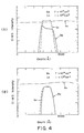
- FIGS.3(A) and (B) show the result of evaluation of the test samples of FIG.2(A) thus formed.
- the compositional profile of Be was measured from the top surface of the GaAlAs layer 35 to the bottom of the GaAlAs layer 33 by secondary ion mass spectroscopy (SIMS), in which FIG.3(A) shows the case in which Be is doped to the layer 34 with a level of 3 X 1019 cm ⁇ 3 and FIG.3(B) shows the case in which Be is doped to the layer 34 with a level of 7 X 1019 cm ⁇ 3.
- the thickness of a region which contains Be is represented as a thickness of a layer containing Be with a concentration level which is one-tenth of the maximum concentration level of Be contained in that region.
- the region of the sample in which Be is contained is confined within a thickness of about 1200 ⁇ in correspondence to the designed layer thickness of the layer 34 when Be is doped within the level of 3 X 1019 cm ⁇ 3. No substantial diffusion of Be beyond the base layer 34 is observed.
- the concentration level of Be is increased to a level of 7 X 1019 cm ⁇ 3
- the thickness of the region in the sample in which Be is contained is broadened to a thickness of about 1500 ⁇ as is clearly seen in FIG.3(B). This means that there is a substantial diffusion of Be from the base layer 34 in agreement with the aforementioned report (Pao, Y.C. et al. op.cit.).
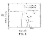
- FIGS.4(A), (B) and (C) show a result of the evaluation for the test sample of FIG.2(B) with a constant doping level of Be at 7 X 1019 cm ⁇ 3 and with various In concentration levels.
- the evaluation was made by SIMS similarly to the foregoing case.
- In is added to Ga 1-x Al x As such that the composition after the addition of In is represented as In y (Ga 1-x Al x ) 1-y As.
- the ratio between Al and Ga is not changed by the addition of In.
- the composition after the addition of In is represented as In y (In x Ga 1-x ) 1-y As.
- the value y is determined by the concentration level of Be to be added for doping as already described. In the case that Be is doped to the level of 5 X 10¹⁹ - 5 X 1020 cm ⁇ 3, a range of y between 0.005 to 0.08 is preferred for eliminating the unwanted abnormal increase of diffusion of Be.
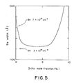
- FIG.5 shows the thickness of the Be-containing region formed in the test sample of FIG.2(B) for various In concentration levels. Similarly to the foregoing experiments, the concentration of Be is fixed at 7 X 1019 cm ⁇ 3. As is clearly seen in this drawing, there is a minimum in the thickness of the Be-containing region in correspondence to the compositional range of about 0.5 mole % to about 8 mole % represented in terms of the InAs component.
- FIG.6 shows a structure of an HBT according to an embodiment of the present invention.
- an n+-type collector buffer layer of GaAs 13 and an n-type collector 14 of GaAs are grown consecutively on a buffer layer of GaAs which in turn is grown on an (100) surface of a semi-insulating GaAs substrate 11.
- the collector buffer layer 13 has a thickness of 5000 ⁇ and a donor concentration level of 3 X 1018 cm ⁇ 3 while the collector layer 14 has a thickness of 3000 ⁇ and a donor concentration level of 5 X 1016 cm ⁇ 3.
- Be is doped typically to a concentration level of about 1 X 1020 cm ⁇ 3
- an n-type emitter layer 20 of GaAlAs and an n+-type emitter cap layer 24 are grown epitaxially on the base layer 16 with the compositional gradient of Al as shown in FIG.7.
- the base layer 16 ordinarily achieves the lattice matching with the collector layer 14 when it is free from In and Be.
- Be is doped to a level of 5 X 10¹⁹ - 5 X 1020 cm ⁇ 3 in order to reduce the base spreading resistance, the lattice matching is lost because of the small atomic radius of Be incorporated into the base layer 16.
- the strain induced in the crystal lattice of the p+-type InGaAlAs base layer 16 by the doping of Be is successfully eliminated by the simultaneous addition of In according to the formula In y (Ga 1-x Al x ) 1-y As, in which the parameter y is set to the foregoing range of 0.005 - 0.08 and the foregoing lattice matching is reestablished.
- the composition x for Al is changed with respect to the composition of Ga represented as 1 - x from a value 0.0 at an interface to the collector layer 14 to 0.1 at another interface to the emitter layer 20 independently of the composition y .
- the n-type emitter layer 20 further comprises a first layer 21 having a thickness of about 300 A and a donor concentration level of about 5 X 1017 cm ⁇ 3 with the aluminium composition ranging from 0.1 to 0.3, a second layer 22 having a thickness of about 900 A and the same donor concentration level with the aluminium composition of 0.3, and a third layer 23 having a thickness of about 300 A and the same donor concentration level with the aluminium composition decreasing from 0.3 to zero as illustrated in FIG.7.
- the compositional gradient of Al as such, the band structure across the collector, base and emitter becomes continuous and the undesirable spike and notch in the band structure is eliminated.
- the n+-type cap layer 24 has a thickness of about 1500 A and a donor concentration level of about 5 X 1018 cm ⁇ 3 On this cap layer 24, an emitter electrode 25 is provided. Similarly, a base electrode 26 is provided on the base layer 14 and a collector electrode 27 is provided on the collector buffer layer 13.
- the growth of the layers 12 - 24, particularly the base layer 16, is preferrably made according to the MBE process already described with reference to the formation of the test sample of FIG.2(B) or MOCVD in which a near-ideal stoichiometry is maintained in the group III-V compound semiconductor layers thus grown.
- the epitaxial growth of the layers 16 and 20 containing Al can be made in the temperature rang of 550 - 680 °C, preferably above 600°C.
- the diffusion of Be to the neighbouring emitter layer 20 or collector layer 14 is effectively prevented even the layers 16 and 20 are grown in such a relatively high temperature range and the destruction of the HBT structure is avoided while still maintaining the graded compositional structure which facilitates the high speed operation of the device.
- the HBT is constructed on a semi-insulating InP substrate 41.
- a buffer layer 43 of undoped InAlAs is grown epitaxially on the substrate 41 for a thickness of about 3000 ⁇ while maintaining the lattice matching with the underlying substrate 41, and an n+-type collector contact layer 45 of InGaAs with a donor concentration level of 2 X 1019 cm ⁇ 3 is grown on the buffer layer 43 for a thickness of 5000 ⁇ .
- an n-type collector layer 47 of InGaAs with a donor concentration level of 3 X 1016 cm ⁇ 3 is grown epitaxially on the collector contact layer 45 for a thickness of 5000 ⁇ .
- the composition of the InGaAs layers 45 and 47 is adjusted to In 0.53 Ga 0.47 As and the composition of the InAlAs buffer layer is adjusted to In 0.52 Al 0.48 As in order to achieve the lattice matching with the underlying InP substrate 41.
- a base layer 49 of InGaAlAs is grown epitaxially for a thickness of about 1000 ⁇ .
- the base layer 49 is doped to the p-type by addition of Be to the concentration level of about 1 X 1020 cm ⁇ 3.
- the composition of the base layer 49 is graded such that the concentration of Al is increased gradually from 0 to 0.2 from a bottom boundary of the base layer 49 to a top boundary thereof.
- the concentration of In is increased from 0.53 to a level corresponding to the concentration of Be according to the foregoing relation.
- the Be concentration level is set in the range of 5 X 10¹⁹ - 5 X 1020 cm ⁇ 3
- In is added according to the formula In y [In 0.53 (Ga 1-x Al x ) 0.47 ] 1-y
- the parameter y changes from 0 to 0.2.
- a first emitter layer 51 of InGaAlAs of the n-type and having a composition of In 0.53 (Ga 1-x Al x ) 0.47 As is grown with the parameter x changing from 0.2 to 1 from the bottom to the top, and a second emitter layer 53 of InAlAs doped to the n-type is grown further thereon.
- the first emitter layer 51 has a thickness of about 300 ⁇ and the second emitter layer 53 has a thickness of about 2000 ⁇ .
- the concentration level of the donor is fixed at about 2 X 1017 cm ⁇ 3.
- a first cap layer 55 of InGaAlAs doped to the n-type with the donor concentration level of about 2 X 1019 cm ⁇ 3 is grown on the second emitter layer 53 for a thickness of about 700 ⁇ while changing the composition from one hundred percent InAlAs at the bottom to one hundred percent InGaAs at the top.
- a second cap layer 57 of InGaAs is grown on the first cap layer 55 for a thickness of about 500 ⁇ .
- the second cap layer 57 is doped to a donor concentration level of about 1 X 1019 cm ⁇ 3.
- an emitter electrode 61 of gold-germanium alloy, a base electrode 62 of gold-zinc alloy, and a collector electrode 63 of gold-germanium allow are provided respectively on the emitter cap layer 57, the base layer 49 and on the collector contact layer 45 and the HBT of this embodiment is completed.
- the growth of the layers 45 through 57 is made by MBE or MOCVD at a temperature of about 600°C or more. Because of the simultaneous doping of Be and In to the base layer 49, the diffusion of Be to the adjacent layers is successfully suppressed in spite of the high temperature employed for the growth of the base layer. Thus, an extremely high speed HBT having the operational speed enhanced by the use of thin but low resistance base layer as well as by the use of the graded compositional profile for the base and the emitter is obtained. Associated with the suppressing of the abnormal diffusion of Be, the reproducibility of the obtained HBT is improved.
Abstract
Description
- The present invention generally relates to semiconductor devices and more particularly to a method of manufacturing a heterojunction bipolar transistor (HBT).
- HBT using a group III-V compound semiconductor material such as gallium arsenide (GaAs) is characterized by a high operational speed. This desirable operational characteristic is obtained mainly as a result of the high electron mobility in the the group III-V compound forming the transistor. Further the use of a material having a large band gap for the emitter also contributes to the increase of the speed of the device.
- In such an HBT, or in a bipolar transistor in general, it is desired that the base of the transistor is made as thin as possible in order to reduce the base transit time of electron and hence to increase the operational speed of the transistor further. However, excessive reduction of the thickness of the base causes an adversary increase of the base spreading resistance which in turn decreases the speed of the transistor. Thus, in order to decrease the thickness of the base without increasing the base spreading resistance, it is desired to dope the base to a doping level as high as possible, for example to a level of about 1
X 10²⁰ cm⁻³. - Meanwhile, it is known that the operational speed of the HBT is further improved by establishing an electric field in the base such that the electron passing therethrough is accelerated. Such an electric field is obtained by providing a compositional gradient in the material forming the base such that there is a large band gap at a side of the base in contact with the emitter and such that the band gap is narrowed continuously toward the collector. For this purpose, gallium aluminium arsenide (GaAlAs) having a composition of Ga1-xAlxAs is used for the base with a gradual change of the composition x ranging from 0 to 0.1. Note that there is substantially no change of lattice constant in the foregoing system and the problem of the lattice mismatch is avoided.
- In an npn-type HBT constructed on a GaAs substrate with a base of GaAs doped to the p-type, beryllium (Be) is used as the dopant for the base. Unfortunately, it is known that the diffusion coefficient of Be in GaAs increases steeply by a factor of one thousand to even ten thousand when the concentration level of Be is increased beyond a level of about 4
X 10¹⁹ cm⁻³ (Pao, Y.C. et al. J. Appl. Phys. 60, 1986, p.201). Further, it is known that such an increase of the diffusion coefficient of Be is further enhanced in the system of GaAlAs (Miller, D.L., J. Appl. Phys. 57, 1985, p. 1816). In other words, there is a tendency that Be is diffused into the neighbouring collector and emitter during the manufacturing process of the transistor, and there is a substantial risk that the conduction type of the emitter and collector is changed or the bipolar structure of the transistor is damaged. As a high temperature of about 600 °C or more is needed for the growth of GaAlAs, the problem of diffusion of Be into the neighbouring collector or emitter becomes worse in the case of the HBT using GaAlAs for the graded base. Thus, the conventional HBT has a problem in that it cannot be constructed to have a sufficiently reduced base thickness as well as a graded base profile to fully exploit the high speed performance of the HBT. - A similar problem appears also when the npn-type HBT is constructed on an indium phosphide (InP) substrate with a base of indium gallium aluminium arsenide (InGaAlAs) sandwiched by a collector and an emitter of indium gallium arsenide. Thus, when Be is doped to a level exceeding about 1 X 10²⁰cm⁻³ in InGaAlAs, the diffusion coefficient of Be is increased significantly.
- On the other hand, there is a known HBT described by Wang et al. (Wang, K.C., Asbeck, P.M., Chang, M.F., Sullivan, G.J. and Miller, D.L., IEEE Electron Device Letters, EDL-8, no.9, September 1987, pp.383 - 385) in which Be is doped to the base with a high concentration level together with an indium arsenide (InAs) component contained in the base by an amount of 10 mole %. In this device, the problem of excessive diffusion of Be is avoided by choosing InGaAs which is free from aluminium (Al) for the base so that the base can be grown in a low temperature range of about 500°C or less. This device, however, does not allow the compositional gradient in the base and thus the device has a limitation in the operational speed. Formation of the compositional gradation by adding elements other than Al to the system of InGaAs is generally not possible because of the unacceptable mismatch of lattice with respect to the collector or emitter.
- Accordingly, it is a general object of the present invention to provide a novel and useful method of manufacturing a heterojunction bipolar transistor wherein the aforementioned problems are eliminated.
- Another and more specific object of the present invention is to provide a method of manufacturing a semiconductor device having an epitaxial layer of a compound semiconductor material containing Be with a high concentration level, wherein the abnormal increase of the diffusion of Be in the epitaxial layer can be suppressed effectively.
- Another object of the present invention is to provide a method of manufacturing a semiconductor device having an epitaxial layer of a p-type compound semiconductor material selected from a group comprising GaAlAs and indium gallium aluminium arsenide (InGaAlAs), with a composition adjusted so as to achieve a lattice matching with an underlying crystal and doped by Be with a concentration level of 5 X 10¹⁹ - 5 X 10²⁰cm⁻³, wherein the epitaxial layer is further added with indium (In) with a level of 0.5 - 8 mole % with respect to the group III elements contained in the epitaxial layer. According to the present invention, the strain induced in the crystal structure of the group III-V compound semiconductor material by the doping of Be having a small atomic radius (1.06 Å) is compensated by addition of In which has a large atomic radius (1.44 Å). As a result, energetical instability of Be associated with the strain energy of the lattice deformation which in turn invites relative lowering of the energy barrier of diffusion is eliminated and the problem of the abnormal increase of the diffusion of Be is avoided. Note that Be and In are distributed at random in the crystallographic site for the group III element in the structure and the overall strain of the crystal lattice is relaxed. As a result of elimination of the abnormal diffusion of Be, the semiconductor device such as HBT can be manufactured without the risk that the semiconductor layers adjacent to the foregoing epitaxial layer are erroneously doped or the structure of the device is destroyed.
- Other objects and further features of the present invention will be apparent from the following detailed description when read in conjunction with attached drawings.
-
- FIGS.1(A) and (B) are schematical diagrams showing the principle of the present invention;
- FIGS.2(A) and (B) are diagrams showing samples used for experiments conducted to demonstrate the suppressing of the diffusion of Be by doping of In;
- FIGS.3(A) and (B) are diagrams showing results of the experiment using the sample of FIG.2(A) corresponding to a prior art;
- FIGS.4(A) - (C) are diagrams showing results of the experiment using the sample of FIG.2(B) corresponding to the present invention;
- FIG.5 is a graph showing the result of the experiment for the sample of FIG.2(B) in correspondence to the present invention while changing the In content;
- FIG.6 is a cross sectional view showing a structure of an HBT manufactured according to a first embodiment of the present invention;
- FIG.7 is a diagram showing a compositional profile of aluminium in the device of FIG.6; and
- FIG.8 is a cross sectional view showing a structure of an HBT manufactured according to a second embodiment of the present invention.
- FIGS.1(A) and (B) show the principle of the present invention. In FIG.1(A) showing a schematical structure of GaAs, a gallium (Ga)
atom 2 and anAs atom 4 are assembled into a zinc blende structure having a face-centered cubic (fcc) packing in which theGa atom 2 occupies a sublattice or site for the group III element having the tetrahedral coordination and theAs atom 4 occupies a sublattice or site for the group V element also having the tetrahedral coordination. In a GaAlAs crystal, Al substitutes a part of Ga. - When a
Be atom 1 is doped with a substantial concentration to the structure of FIG.1(A), the Be atom thus doped substitutes a part of theGa atoms 2 as shown in FIG.1(B). Thereby, there appears a distortion or deformation in the crystal structure particularly when the concentration level of Be is increased to a range of about 5 X 10¹⁹ - 5 X 10²⁰cm⁻³, as the Be atom has a substantially smaller atomic radius as compared to Ga atom or Al atom. - The following Table I summarizes the atomic radius for Be and the group III as well as group V elements involved in the HBT of the present invention.
TABLE I Atomic radius of typical group III and group V elements as well as Be used for doping of group III-V compound. Be 1.06 Å Al 1.26 Å Ga 1.26 Å In 1.44 Å As 1.18 Å - In the present invention, it was found that the abnormal increase of the diffusion of Be in the compound or system of GaAlAs or InGaAlAs is suppressed significantly by introducing In with an amount of about 0.5 to 8 mole % with respect to the group III elements in the system. As a result of simultaneous addition of an
In atom 3 together with theBe atom 1, the strain formed in the crystal structure is relaxed as shown in FIG.1(B). It is believed that such a relaxation of the strain of the crystal structure causes the relative lowering of the energy of Be in the structure and the energy barrier for diffusion of Be is relatively increased as compared to the potential energy of Be. As a result of such a relative increase of the energy barrier of diffusion, the abnormal diffusion of Be into the neighbouring semiconductor layers is successfully eliminated. - FIGS.2(A) and (B) show the construction of test samples used to demonstrate the effect of eliminating the abnormal diffusion of Be by simultaneous addition of In according to the present invention in comparison with a prior art method in which no such simultaneous addition of In is made.
- Referring to FIG.2(A) showing a test sample produced according to the prior art method, a
buffer layer 32 of GaAs is grown epitaxially on a (100) surface of aGaAs substrate 31 for a thickness of 500 Å and anGaAlAs layer 33 having a composition of Ga0.9Al0.1As is grown further on thebuffer layer 32 for a thickness of 2100 Å. On the GaAlAslayer 33, another GaAlAslayer 34 doped to the p-type and having the same composition Ga0.9Al0.1As is grown for a thickness of 1000 Å. In this test sample, the thickness of thelayer 34 is set larger than the actual thickness of the base of a typical HBT in order to examine the diffusion of Be in detail. Further, another GaAlAslayer 35 having also the same composition Ga0.9Al0.1As is grown on thelayer 34. In the drawing, the ordinate represents the composition of aluminium (Al) in the layers 31 - 35. - FIG.2(B) shows the structure of a test sample corresponding to the present invention. In this drawing, these portions corresponding to the portions described with reference to FIG.2(A) are given the identical reference numerals and the description thereof will be omitted.
- In this test sample, after the epitaxial growth of the
buffer layer 32 for a thickness of 500 Å on thesubstrate 31, a GaAlAs layer 33a having a composition of Ga0.9Al0.1As is grown on thebuffer layer 32 for a thickness of 2000 Å. Next, alower boundary layer 36 having a composition of Ga0.9Al0.1As and added with In is grown on the buffer layer 33a for a thickness of 100 Å, and a p-type GaAlAs layer 37 is grown on thelower boundary layer 35 together with the addition of In and further with Be for a thickness of 1000 Å. Further, an upper boundary layer 39 of GaAlAs having a composition of Ga0.9Al0.1As and added with In is grown on the p-type layer 37 with a thickness of 100 Å. Further, a still another GaAlAs layer 35a having the same composition of Ga0.9Al0.1As is grown with a thickness of 3000 Å. The In concentration with respect to the total amount of Ga and Al is maintained the same throughout the layers 36 - 38. Further, a number of test samples having the structure of FIG.2(B) are prepared with various concentration levels for In. Note that the ordinate in FIG.2(B) represents the Al composition similarly to the case of FIG.2(A). - In both of the test samples, the growth of the layers is made by molecular beam epitaxy (MBE) at a temperature of 600°C with a growth rate of 1 µm/hour. During the growth, the vapor pressure of As is controlled at 4
X 10⁻⁵ Torr, and the temperature of the cells for holding the source materials of Al and Ga is controlled such that the composition ratio of Al and Ga in the obtained semiconductor layer is maintained at 1 : 9. Further, the temperature of the cells for holding the source material of Be and In is controlled so as to establish a predetermined concentration level for these elements. As a result, Be alone or Be and In together are incorporated into the crystallographic site for the group III element of GaAlAs during the growth of thelayer 37. - FIGS.3(A) and (B) show the result of evaluation of the test samples of FIG.2(A) thus formed. In this evaluation, the compositional profile of Be was measured from the top surface of the
GaAlAs layer 35 to the bottom of theGaAlAs layer 33 by secondary ion mass spectroscopy (SIMS), in which FIG.3(A) shows the case in which Be is doped to thelayer 34 with a level of 3X 10¹⁹ cm⁻³ and FIG.3(B) shows the case in which Be is doped to thelayer 34 with a level of 7X 10¹⁹ cm⁻³. In the description hereinafter, the thickness of a region which contains Be is represented as a thickness of a layer containing Be with a concentration level which is one-tenth of the maximum concentration level of Be contained in that region. - As is clearly seen from FIG.3(A), the region of the sample in which Be is contained is confined within a thickness of about 1200 Å in correspondence to the designed layer thickness of the
layer 34 when Be is doped within the level of 3X 10¹⁹ cm⁻³. No substantial diffusion of Be beyond thebase layer 34 is observed. On the other hand, when the concentration level of Be is increased to a level of 7X 10¹⁹ cm⁻³, the thickness of the region in the sample in which Be is contained is broadened to a thickness of about 1500 Å as is clearly seen in FIG.3(B). This means that there is a substantial diffusion of Be from thebase layer 34 in agreement with the aforementioned report (Pao, Y.C. et al. op.cit.). - FIGS.4(A), (B) and (C) show a result of the evaluation for the test sample of FIG.2(B) with a constant doping level of Be at 7
X 10¹⁹ cm⁻³ and with various In concentration levels. The evaluation was made by SIMS similarly to the foregoing case. - Referring to FIG.4(A) corresponding to the Be concentration level of 7
X 10¹⁹ cm⁻³ and the In concentration level of 1 X 10²¹ cm⁻³, there appears a similar broadening of the Be-containing region reaching a thickness of about 1800 Å similarly to the case of FIG.3(B). In other words, there exists a similar abnormal increase of Be diffusion in this case. - When the In concentration level is reduced to 1
X 10¹⁹ cm⁻³ (FIG.4(B)), on the other hand, it can be seen that the thickness of the portion containing Be in the test sample is confined in the range of about 1200 Å even when thelayer 37 is doped with Be to the concentration level of 7X 10¹⁹ cm⁻³. In other words, the abnormal increase of the diffusion of Be is effectively suppressed when the In content in theGaAlAs layer 37 is chosen as such. - When the content or concentration level of In is further reduced to below 5
X 10¹⁹ cm⁻³ which is the detection limit of SIMS, it can be seen from FIG.4(C) that the broadening of the Be-containing region is again increased to an extent of about 1500 Å similarly to that of FIG.3(B). In this case, it is understood that the suppression of the abnormal diffusion of Be is not effective because of the too small concentration level of In. - Note that a similar tendency is observed also in the system of GaAs, InGaAs or InGaAlAs. In general, it was found that the abnormal increase of the diffusion coefficient of Be is suppressed by adding In according to a formula of Iny(III)1-y(V) simultaneously to the doping of Be where (III) represents the group III elements, (V) represents the group V elements, and y = 0 represents the hypothetical composition in which there is no doping of Be. The composition y is determined generally proportional to the amount of Be added for the doping. By adding In as such, the ratio between two or more group III elements, which is usually determined to achieve a lattice matching with adjacent layers, is maintained. For example, In is added to Ga1-xAlxAs such that the composition after the addition of In is represented as Iny(Ga1-xAlx)1-yAs. Obviously, the ratio between Al and Ga is not changed by the addition of In. When In is added to a system already including In such as InxGa1-xAs, the composition after the addition of In is represented as Iny(InxGa1-x)1-yAs. The value y is determined by the concentration level of Be to be added for doping as already described. In the case that Be is doped to the level of 5 X 10¹⁹ - 5
X 10²⁰ cm⁻³, a range of y between 0.005 to 0.08 is preferred for eliminating the unwanted abnormal increase of diffusion of Be. - FIG.5 shows the thickness of the Be-containing region formed in the test sample of FIG.2(B) for various In concentration levels. Similarly to the foregoing experiments, the concentration of Be is fixed at 7
X 10¹⁹ cm⁻³. As is clearly seen in this drawing, there is a minimum in the thickness of the Be-containing region in correspondence to the compositional range of about 0.5 mole % to about 8 mole % represented in terms of the InAs component. - The foregoing results clearly indicate that the abnormal diffusion of Be is suppressed by simultaneous addition of In to the system. The reason of this is attributed to the aforementioned compensation of the strain of the crystal lattice induced by Be by the further addition of In. As a result of the relaxation of the lattice strain, it is believed that Be is stabilized energetically as compared to the energy barrier for the diffusion of Be. According to this theory, it is predicted that there holds a relation:
(vGa - vBe)NBe = (vIn - vGa)NIn
where vGa, vBe, vIn respectively stand for the atomic volume of Ga, Be and In, and NBe and NIN stand for the number of atoms of Be and In, respectively. In this case, a relation NIn = 0.8 X NBe is predicted. In other words, it is predicted that a simultaneous doping of In with an amount which is approximately the same as that of Be is effective for the suppressing of the abnormal diffusion of Be. The results shown in FIGS.4(A) - (C) and FIG.5 supports this prediction. Thus, when the concentration level of In is too small as in the case of FIG.4(C), the abnormal diffusion of Be is not suppressed effectively because of the remaining strain in the crystal lattice. On the other hand, when the concentration of In is too high as in the case of FIG.4(A), there is induced a strain in the crystal lattice as a result of the too high concentration of In. The reason of the appearance of the optimum range of In for a given Be concentration level as shown in FIG.5 is thus explained reasonably according to the foregoing theory. It would be obvious that the suppressing of the abnormal diffusion of Be by the simultaneous doping of In is not limited to the system of GaAlAs but is applicable also to other systems. - Next, an HBT manufactured according to the present invention will be described. FIG.6 shows a structure of an HBT according to an embodiment of the present invention. In this device, an n⁺-type collector buffer layer of
GaAs 13 and an n-type collector 14 of GaAs are grown consecutively on a buffer layer of GaAs which in turn is grown on an (100) surface of a semi-insulating GaAs substrate 11. Thecollector buffer layer 13 has a thickness of 5000 Å and a donor concentration level of 3 X 10¹⁸ cm⁻³ while thecollector layer 14 has a thickness of 3000 Å and a donor concentration level of 5 X 10¹⁶ cm⁻³. - On the
collector layer 14 of GaAs, a p+-type base layer 16 of InGaAlAs doped with Be and having a composition adjusted so as to maintain the lattice matching with theunderlying collector layer 14, is grown epitaxially for a thickness of about 1000 Å, for example, with a compositional gradient of Al as shown in FIG.7. Be is doped typically to a concentration level of about 1X 10²⁰ cm⁻³ Further, an n-type emitter layer 20 of GaAlAs and an n⁺-typeemitter cap layer 24 are grown epitaxially on thebase layer 16 with the compositional gradient of Al as shown in FIG.7. Note that thebase layer 16 ordinarily achieves the lattice matching with thecollector layer 14 when it is free from In and Be. When Be is doped to a level of 5 X 10¹⁹ - 5X 10²⁰ cm⁻³ in order to reduce the base spreading resistance, the lattice matching is lost because of the small atomic radius of Be incorporated into thebase layer 16. In the present embodiment, the strain induced in the crystal lattice of the p⁺-typeInGaAlAs base layer 16 by the doping of Be is successfully eliminated by the simultaneous addition of In according to the formula Iny(Ga1-xAlx)1-yAs, in which the parameter y is set to the foregoing range of 0.005 - 0.08 and the foregoing lattice matching is reestablished. Note that the composition x for Al is changed with respect to the composition of Ga represented as 1 - x from a value 0.0 at an interface to thecollector layer 14 to 0.1 at another interface to theemitter layer 20 independently of the composition y. Thus, there is established an electrical field which accelerates the electron passing through thebase layer 16 similarly to the case that there is no doping of In. - The n-
type emitter layer 20 further comprises afirst layer 21 having a thickness of about 300 A and a donor concentration level of about 5 X 10¹⁷ cm⁻³ with the aluminium composition ranging from 0.1 to 0.3, a second layer 22 having a thickness of about 900 A and the same donor concentration level with the aluminium composition of 0.3, and athird layer 23 having a thickness of about 300 A and the same donor concentration level with the aluminium composition decreasing from 0.3 to zero as illustrated in FIG.7. As a result of the compositional gradient of Al as such, the band structure across the collector, base and emitter becomes continuous and the undesirable spike and notch in the band structure is eliminated. - The n⁺-
type cap layer 24 has a thickness of about 1500 A and a donor concentration level of about 5 X 10¹⁸ cm⁻³ On thiscap layer 24, anemitter electrode 25 is provided. Similarly, abase electrode 26 is provided on thebase layer 14 and acollector electrode 27 is provided on thecollector buffer layer 13. - The growth of the layers 12 - 24, particularly the
base layer 16, is preferrably made according to the MBE process already described with reference to the formation of the test sample of FIG.2(B) or MOCVD in which a near-ideal stoichiometry is maintained in the group III-V compound semiconductor layers thus grown. The epitaxial growth of thelayers base layer 16 together with Be, the diffusion of Be to the neighbouringemitter layer 20 orcollector layer 14 is effectively prevented even thelayers - Next, a second embodiment of the HBT will be described with reference to FIG.8. In this embodiment, the HBT is constructed on a
semi-insulating InP substrate 41. Referring to FIG.8, abuffer layer 43 of undoped InAlAs is grown epitaxially on thesubstrate 41 for a thickness of about 3000 Å while maintaining the lattice matching with the underlyingsubstrate 41, and an n⁺-typecollector contact layer 45 of InGaAs with a donor concentration level of 2X 10¹⁹ cm⁻³ is grown on thebuffer layer 43 for a thickness of 5000 Å. Further, an n-type collector layer 47 of InGaAs with a donor concentration level of 3 X 10¹⁶ cm⁻³ is grown epitaxially on thecollector contact layer 45 for a thickness of 5000 Å. The composition of the InGaAs layers 45 and 47 is adjusted to In0.53Ga0.47As and the composition of the InAlAs buffer layer is adjusted to In0.52Al0.48As in order to achieve the lattice matching with theunderlying InP substrate 41. On a collector structure thus formed, abase layer 49 of InGaAlAs is grown epitaxially for a thickness of about 1000 Å. Thebase layer 49 is doped to the p-type by addition of Be to the concentration level of about 1X 10²⁰ cm⁻³. Note that the composition of thebase layer 49 is graded such that the concentration of Al is increased gradually from 0 to 0.2 from a bottom boundary of thebase layer 49 to a top boundary thereof. At the same time to the doping of thebase layer 49 by Be, the concentration of In is increased from 0.53 to a level corresponding to the concentration of Be according to the foregoing relation. When the Be concentration level is set in the range of 5 X 10¹⁹ - 5X 10²⁰ cm⁻³, In is added according to the formula
Iny[In0.53(Ga1-xAlx)0.47]1-yAs with the parameter y set in the range of 0.008 - 0.05. As a result of the foregoing compositional grading of Al, the parameter x changes from 0 to 0.2. - On the
base layer 49, afirst emitter layer 51 of InGaAlAs of the n-type and having a composition of In0.53(Ga1-xAlx)0.47As is grown with the parameter x changing from 0.2 to 1 from the bottom to the top, and asecond emitter layer 53 of InAlAs doped to the n-type is grown further thereon. Thefirst emitter layer 51 has a thickness of about 300 Å and thesecond emitter layer 53 has a thickness of about 2000 Å. In both of the first and second emitter layers 51 and 53, the concentration level of the donor is fixed at about 2 X 10¹⁷ cm⁻3. - Further, a
first cap layer 55 of InGaAlAs doped to the n-type with the donor concentration level of about 2X 10¹⁹ cm⁻³ is grown on thesecond emitter layer 53 for a thickness of about 700 Å while changing the composition from one hundred percent InAlAs at the bottom to one hundred percent InGaAs at the top. Furthermore, asecond cap layer 57 of InGaAs is grown on thefirst cap layer 55 for a thickness of about 500 Å. Thesecond cap layer 57 is doped to a donor concentration level of about 1X 10¹⁹ cm⁻³. As a result of the compositional gradation for the emitter layers 51 and 53 and for the cap layers 55 and 57, the undesirable spikes and notches are eliminated from the band structure. Finally, anemitter electrode 61 of gold-germanium alloy, abase electrode 62 of gold-zinc alloy, and acollector electrode 63 of gold-germanium allow are provided respectively on theemitter cap layer 57, thebase layer 49 and on thecollector contact layer 45 and the HBT of this embodiment is completed. - Similarly to the foregoing embodiment, the growth of the
layers 45 through 57 is made by MBE or MOCVD at a temperature of about 600°C or more. Because of the simultaneous doping of Be and In to thebase layer 49, the diffusion of Be to the adjacent layers is successfully suppressed in spite of the high temperature employed for the growth of the base layer. Thus, an extremely high speed HBT having the operational speed enhanced by the use of thin but low resistance base layer as well as by the use of the graded compositional profile for the base and the emitter is obtained. Associated with the suppressing of the abnormal diffusion of Be, the reproducibility of the obtained HBT is improved.
Claims (13)
Applications Claiming Priority (2)
| Application Number | Priority Date | Filing Date | Title |
|---|---|---|---|
| JP271345/88 | 1988-10-27 | ||
| JP27134588 | 1988-10-27 |
Publications (3)
| Publication Number | Publication Date |
|---|---|
| EP0366552A2 true EP0366552A2 (en) | 1990-05-02 |
| EP0366552A3 EP0366552A3 (en) | 1990-11-28 |
| EP0366552B1 EP0366552B1 (en) | 1993-04-28 |
Family
ID=17498768
Family Applications (1)
| Application Number | Title | Priority Date | Filing Date |
|---|---|---|---|
| EP89402953A Expired - Lifetime EP0366552B1 (en) | 1988-10-27 | 1989-10-25 | Method of manufacturing a heterojunction bipolar transistor |
Country Status (2)
| Country | Link |
|---|---|
| EP (1) | EP0366552B1 (en) |
| DE (1) | DE68906239T2 (en) |
Cited By (3)
| Publication number | Priority date | Publication date | Assignee | Title |
|---|---|---|---|---|
| US5429957A (en) * | 1992-08-17 | 1995-07-04 | Matsushita Electric Industrial Co., Ltd. | Method of manufacturing an heterojunction bipolar transistor |
| EP0746035A2 (en) * | 1995-06-02 | 1996-12-04 | Trw Inc. | Quarternary collector InA1As-InGaA1As heterojunction bipolar transistor |
| GB2344462A (en) * | 1998-12-02 | 2000-06-07 | Arima Optoelectronics Corp | Doping semiconductor devices |
-
1989
- 1989-10-25 DE DE1989606239 patent/DE68906239T2/en not_active Expired - Fee Related
- 1989-10-25 EP EP89402953A patent/EP0366552B1/en not_active Expired - Lifetime
Non-Patent Citations (6)
| Title |
|---|
| Appl. Phys. Lett. 37(1) 1July 1980 p.64-65. * |
| APPLIED PHYSICS LETTERS, vol. 53, no 11, 12th September 1988, pages 983-985, American Institute of Physics, New York, US; W.T. TSANG et al.: "GalnAs/GalnAsP/InP heterostructure bipolar transistors with very thin base (150 A) grown by chemical beam epitaxy" * |
| IEEE ELECTRON DEVICE LETTERS, vol. EDL-8, no. 9, September 1987, pages 383-385, New York, US; K.C. WANG et al.: "A 20-GHz frequency divider implemented with heterojunction bipolar transistors" * |
| INTERNATIONAL ELECTRON DEVICES MEETING, TECHNICAL DIGEST, Los Angeles, CA, 7th - 10th December 1986, pages 89-92, IEEE, New York, US; K. OHTA et al.: "Theory and experiment of heterojuncion bipolar transistor at very low temperatures" * |
| JAPANESE JOURNAL OF APPLIED PHYSICS, vol. 25, no. 10, part 2, October 1986, pages L862-L864, Tokyo, JP; A. FURUKAWA et al.: "4.2 K operation of InAlAs/InGaAs heterojunction bipolar transistor" * |
| Journal of Crystal Growth 46(1979) 300-303. * |
Cited By (5)
| Publication number | Priority date | Publication date | Assignee | Title |
|---|---|---|---|---|
| US5429957A (en) * | 1992-08-17 | 1995-07-04 | Matsushita Electric Industrial Co., Ltd. | Method of manufacturing an heterojunction bipolar transistor |
| EP0746035A2 (en) * | 1995-06-02 | 1996-12-04 | Trw Inc. | Quarternary collector InA1As-InGaA1As heterojunction bipolar transistor |
| EP0746035A3 (en) * | 1995-06-02 | 1998-03-11 | Trw Inc. | Quarternary collector InA1As-InGaA1As heterojunction bipolar transistor |
| GB2344462A (en) * | 1998-12-02 | 2000-06-07 | Arima Optoelectronics Corp | Doping semiconductor devices |
| GB2344462B (en) * | 1998-12-02 | 2001-05-16 | Arima Optoelectronics Corp | Semiconductor devices |
Also Published As
| Publication number | Publication date |
|---|---|
| EP0366552B1 (en) | 1993-04-28 |
| DE68906239D1 (en) | 1993-06-03 |
| EP0366552A3 (en) | 1990-11-28 |
| DE68906239T2 (en) | 1993-08-12 |
Similar Documents
| Publication | Publication Date | Title |
|---|---|---|
| EP0619613B1 (en) | A heterojunction bipolar transistor | |
| US5770868A (en) | GaAs substrate with compositionally graded AlGaAsSb buffer for fabrication of high-indium fets | |
| JP3224437B2 (en) | III-V compound semiconductor device | |
| EP0381396A1 (en) | Compound semiconductor devices | |
| US5952672A (en) | Semiconductor device and method for fabricating the same | |
| EP0740350B1 (en) | Compound semiconductor device having reduced resistance | |
| US5284783A (en) | Method of fabricating a heterojunction bipolar transistor | |
| EP0366552B1 (en) | Method of manufacturing a heterojunction bipolar transistor | |
| US5814843A (en) | Heterojunction bipolar transistor having a graded-composition base region | |
| US7291873B2 (en) | High electron mobility epitaxial substrate | |
| US7732836B2 (en) | Compound semiconductor epitaxial substrate and method for manufacturing the same | |
| US6429103B1 (en) | MOCVD-grown emode HIGFET buffer | |
| Houng | CBE growth of AlGaAs/GaAs heterostructures and their device applications | |
| JP2761264B2 (en) | Method for manufacturing semiconductor device | |
| JPH03124033A (en) | Heterojunction bipolar transistor | |
| KR100519896B1 (en) | High-concentration doped semiconductor and method of fabricating the same | |
| Ando et al. | Growth of carbon-doped base GaAs/AlGaAs HBT by gas-source MBE using TEG, TEA, TMG, AsH3, and Si2H6 | |
| JP2980630B2 (en) | Compound semiconductor device | |
| WO2000007248A1 (en) | High electron mobility transistor | |
| Kobayashi et al. | Growth temperature dependence of Zn diffusion in InPInGaAs heterojunction bipolar transistor structures grown by metalorganic chemical vapor deposition | |
| JP3347175B2 (en) | Semiconductor device and manufacturing method thereof | |
| JPH06267867A (en) | Crystal growing method of compound semiconductor and formation of ohmic contact using same | |
| Sandhu et al. | p+/N GaAs-AlGaAs heterostructures grown by gas source MBE using gaseous p-and n-type dopant sources | |
| Fujii et al. | Suppression of Be diffusion in molecular‐beam epitaxy AlGaAs by the incorporation of In for heterojunction bipolar transistor applications | |
| Watanabe et al. | Reduction of recombination centers in C‐doped p+‐GaAs/n‐AlGaAs heterojunctions by post‐growth annealing |
Legal Events
| Date | Code | Title | Description |
|---|---|---|---|
| PUAI | Public reference made under article 153(3) epc to a published international application that has entered the european phase |
Free format text: ORIGINAL CODE: 0009012 |
|
| AK | Designated contracting states |
Kind code of ref document: A2 Designated state(s): DE FR GB |
|
| PUAL | Search report despatched |
Free format text: ORIGINAL CODE: 0009013 |
|
| AK | Designated contracting states |
Kind code of ref document: A3 Designated state(s): DE FR GB |
|
| RHK1 | Main classification (correction) |
Ipc: H01L 29/73 |
|
| 17P | Request for examination filed |
Effective date: 19901221 |
|
| 17Q | First examination report despatched |
Effective date: 19920511 |
|
| GRAA | (expected) grant |
Free format text: ORIGINAL CODE: 0009210 |
|
| AK | Designated contracting states |
Kind code of ref document: B1 Designated state(s): DE FR GB |
|
| REF | Corresponds to: |
Ref document number: 68906239 Country of ref document: DE Date of ref document: 19930603 |
|
| ET | Fr: translation filed | ||
| PLBE | No opposition filed within time limit |
Free format text: ORIGINAL CODE: 0009261 |
|
| STAA | Information on the status of an ep patent application or granted ep patent |
Free format text: STATUS: NO OPPOSITION FILED WITHIN TIME LIMIT |
|
| 26N | No opposition filed | ||
| REG | Reference to a national code |
Ref country code: GB Ref legal event code: IF02 |
|
| PGFP | Annual fee paid to national office [announced via postgrant information from national office to epo] |
Ref country code: DE Payment date: 20071018 Year of fee payment: 19 |
|
| PGFP | Annual fee paid to national office [announced via postgrant information from national office to epo] |
Ref country code: GB Payment date: 20071024 Year of fee payment: 19 Ref country code: FR Payment date: 20071009 Year of fee payment: 19 |
|
| GBPC | Gb: european patent ceased through non-payment of renewal fee |
Effective date: 20081025 |
|
| REG | Reference to a national code |
Ref country code: FR Ref legal event code: ST Effective date: 20090630 |
|
| PG25 | Lapsed in a contracting state [announced via postgrant information from national office to epo] |
Ref country code: DE Free format text: LAPSE BECAUSE OF NON-PAYMENT OF DUE FEES Effective date: 20090501 |
|
| PG25 | Lapsed in a contracting state [announced via postgrant information from national office to epo] |
Ref country code: FR Free format text: LAPSE BECAUSE OF NON-PAYMENT OF DUE FEES Effective date: 20081031 |
|
| PG25 | Lapsed in a contracting state [announced via postgrant information from national office to epo] |
Ref country code: GB Free format text: LAPSE BECAUSE OF NON-PAYMENT OF DUE FEES Effective date: 20081025 |