EP0366459B1 - Method of repairing liquid crystal display and apparatus using the method - Google Patents
Method of repairing liquid crystal display and apparatus using the method Download PDFInfo
- Publication number
- EP0366459B1 EP0366459B1 EP89311040A EP89311040A EP0366459B1 EP 0366459 B1 EP0366459 B1 EP 0366459B1 EP 89311040 A EP89311040 A EP 89311040A EP 89311040 A EP89311040 A EP 89311040A EP 0366459 B1 EP0366459 B1 EP 0366459B1
- Authority
- EP
- European Patent Office
- Prior art keywords
- liquid crystal
- crystal display
- laser beam
- ring
- pixel electrode
- Prior art date
- Legal status (The legal status is an assumption and is not a legal conclusion. Google has not performed a legal analysis and makes no representation as to the accuracy of the status listed.)
- Expired - Lifetime
Links
Images

Classifications
-
- G—PHYSICS
- G02—OPTICS
- G02F—OPTICAL DEVICES OR ARRANGEMENTS FOR THE CONTROL OF LIGHT BY MODIFICATION OF THE OPTICAL PROPERTIES OF THE MEDIA OF THE ELEMENTS INVOLVED THEREIN; NON-LINEAR OPTICS; FREQUENCY-CHANGING OF LIGHT; OPTICAL LOGIC ELEMENTS; OPTICAL ANALOGUE/DIGITAL CONVERTERS
- G02F1/00—Devices or arrangements for the control of the intensity, colour, phase, polarisation or direction of light arriving from an independent light source, e.g. switching, gating or modulating; Non-linear optics
- G02F1/01—Devices or arrangements for the control of the intensity, colour, phase, polarisation or direction of light arriving from an independent light source, e.g. switching, gating or modulating; Non-linear optics for the control of the intensity, phase, polarisation or colour
- G02F1/13—Devices or arrangements for the control of the intensity, colour, phase, polarisation or direction of light arriving from an independent light source, e.g. switching, gating or modulating; Non-linear optics for the control of the intensity, phase, polarisation or colour based on liquid crystals, e.g. single liquid crystal display cells
- G02F1/133—Constructional arrangements; Operation of liquid crystal cells; Circuit arrangements
- G02F1/1333—Constructional arrangements; Manufacturing methods
- G02F1/1343—Electrodes
- G02F1/13439—Electrodes characterised by their electrical, optical, physical properties; materials therefor; method of making
-
- G—PHYSICS
- G02—OPTICS
- G02F—OPTICAL DEVICES OR ARRANGEMENTS FOR THE CONTROL OF LIGHT BY MODIFICATION OF THE OPTICAL PROPERTIES OF THE MEDIA OF THE ELEMENTS INVOLVED THEREIN; NON-LINEAR OPTICS; FREQUENCY-CHANGING OF LIGHT; OPTICAL LOGIC ELEMENTS; OPTICAL ANALOGUE/DIGITAL CONVERTERS
- G02F1/00—Devices or arrangements for the control of the intensity, colour, phase, polarisation or direction of light arriving from an independent light source, e.g. switching, gating or modulating; Non-linear optics
- G02F1/01—Devices or arrangements for the control of the intensity, colour, phase, polarisation or direction of light arriving from an independent light source, e.g. switching, gating or modulating; Non-linear optics for the control of the intensity, phase, polarisation or colour
- G02F1/13—Devices or arrangements for the control of the intensity, colour, phase, polarisation or direction of light arriving from an independent light source, e.g. switching, gating or modulating; Non-linear optics for the control of the intensity, phase, polarisation or colour based on liquid crystals, e.g. single liquid crystal display cells
- G02F1/1306—Details
- G02F1/1309—Repairing; Testing
Landscapes
- Physics & Mathematics (AREA)
- Nonlinear Science (AREA)
- Chemical & Material Sciences (AREA)
- Crystallography & Structural Chemistry (AREA)
- General Physics & Mathematics (AREA)
- Optics & Photonics (AREA)
- Mathematical Physics (AREA)
- Liquid Crystal (AREA)
- Laser Beam Processing (AREA)
Description
- The present invention relates to a method of repairing a foreign matter-containing liquid crystal display by utilizing a laser beam, and an apparatus using the method.
- A liquid crystal display is made up of a common electrode, pixel electrodes facing the common electrode, and liquid crystal sealed between the common electrode and the pixel electrodes. During the manufacturing process of a liquid crystal display, it may happen that electrically-conductive foreign matter is included in the liquid crystal when this liquid crystal is sealed between the common electrode and the pixel electrodes. If the liquid crystal contains foreign matter, the pixel electrode in contact with the foreign matter will be short-circuited to the common electrode. As a result, the liquid crystal display will not operate in response to the ON/OFF operation of a transistor, so that light will be always transmitted through the pixel portions of the pixel electrode which is in contact with the foreign matter.
- One object of the present invention is to provide a method of reliably repairing, by use of a laser beam, a liquid crystal display wherein the common electrode and pixel electrodes are short-circuited to each other, due to electrically-conductive foreign matter included in the liquid crystal.
- Another object of the present invention is to provide an apparatus for reliably repairing, by use of a laser beam, a liquid crystal display wherein the common electrode and pixel electrodes are short-circuited to each other due to electrically-conductiove foreign matter included in the liquid crystal.
- According to the method of the present invention as set forth in
claim 1, a laser beam is applied to a pixel electrode in a form of a ring line completely surrounding that part of the pixel electrode which is in contact with foreign matter, to thereby electrically insulate the portion inside the ring line from the portion outside the ring line. - According to another aspect of the present invention, there is provided an apparatus for repairing a liquid crystal display having a common electrode, a plurality of pixel electrodes facing the common electrode, and a liquid crystal sealed between the common and pixel electrides, the display having a defect comprising conductive foreign matter which short-circuits the common electrode and a said pixel electrode to each other, characterised by comprising: laser oscillating means for generating a laser beam; alignment beam source means for outputting an alignment beam used for alignment of the laser beam generated from said laser oscillating means; first optical means for shaping the laser beam and the alignment beam in such a manner that the laser beam and the alignment beam have a ring-shaped cross-section; XY carriage means on which the liquid crystal display is mounted and which is movable in an XY plane; driving means for driving the liquid crystal display; second optical means for focusing the laser beam and the alignment beam, the cross sections of which are ring-shaped, on a predetermined portion of the liquid crystal display; illuminating means for illuminating the liquid crystal display by directing light thereto through the second optical means; image sensor means picking an image of the liquid crystal display through the second optical means, to generate an image signal; monitor means for visualizing the image signal supplied from said image sensor means to allow detection of the said pixel electrode which is in contact with the foreign matter; whereby a ring-like region of the pixel electrode which surrounds the electrode portion touching the foreign matter can be removed by the laser beam to electrically isolate the pixel electrode portion touching the foreign matter from the pixel electrode portion outside of said ring-like region.
- In the above apparatus, the alignment beam emitted from the alignment beam source is defined in such a manner as to become a ring-like beam, and is then directed to the liquid crystal display by the beam-focusing optical system. In this condition, the liquid crystal display is image-picked up and its image is displayed on the monitor television set. When the alignment beam is directed to the liquid crystal display, it is positioned such that it surrounds foreign matter contained in the liquid crystal display. Thereafter, the laser beam emitted from the laser oscillator is directed to the liquid crystal display, via the same optical path as that of the alignment beam. As a result, the portion which is in contact with the foreign matter and is surround by the alignment beam is electrically insulated from the other portions of the liquid crystal display.
- This invention can be more fully understood from the following detailed description when taken in conjunction with the accompanying drawings, in which:
- Fig. 1 is a diagram showing the arrangement of a liquid crystal display-repairing apparatus according to one embodiment of the present invention;
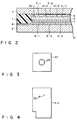
- Fig. 2 is a view showing the construction of a liquid crystal display;
- Fig. 3 is a view of the slit plate employed in the apparatus shown in Fig. 1;
- Fig. 4 is a sketch showing the position of an electrode to be eliminated by the apparatus;
- Fig. 5 is a sketch showing one possible manner in which the electrode is eliminated by the apparatus;
- Fig. 6 is a sketch showing another possible manner in which the electrode is eliminated by the apparatus;
- Fig. 7 is a diagram showing the construction of a scanning device for eliminating the electrode in the manner shown in Fig. 6, the scanning device using a spot laser beam;
- Fig. 8A is a view of a slit plate in which arcuate slits are formed; and
- Fig. 8B illustrates a state in which the slit plate shown in Fig. 8A has been rotated.
- As is shown in Fig. 1,
liquid crystal display 21 is mounted on XY table 20. This liquid crystal display has a construction such as that shown in Fig. 2. Referring to Fig. 2,liquid crystal display 21 comprisesspacer 1 serving as a support member.Translucent glass substrates Common electrode 4 is located betweenglass substrates spacer 1 andglass substrate 2. A plurality of pixel electrodes 5-1, 5-2 ... are arranged onglass substrate 3 such that they facecommon electrode 4. A plurality of color filters 6-1, 6-2 ..., each having one of the three fundamental colors, are arranged betweencommon electrode 4 andglass substrate 2 such that they correspond in location to pixel electrodes 5-1, 5-2..., respectively. Located betweencommon electrode 4 and pixels 5-1, 5-2 ... areorientation films orientation films glass substrate 3. Liquid crystal 9 is supported by use of resin containing fine glass particles, and has a thickness of 5 to 6 µm. - To show a color image on
liquid crystal display 21, light Q is made to fall onliquid crystal 9 throughglass substrate 3. In this state, a voltage is applied betweencommon electrode 4 and given ones of pixel electrodes 5-1, 5-2 .... As a result, the light rays having the wavelengths determined by color filters 6-1, 6-2 ... are transmitted through the pixels corresponding to the given pixel electrodes. - As is shown in Fig. 1, XY table 20 has
hole 22 formed in the center thereof, and transmitted-illumination unit 23 is located under XY table 20. White light P1 emitted from back-light illumination unit 23 is directed toliquid crystal display 21 viahole 22.Liquid crystal display 21 is driven, with thin film transistors 10-1, 10-2 ... selectively turned on or off by liquid crystal display-drivingunit 24. - Laser oscillator 30 is a YAG laser oscillator which emits laser beam R used for working materials. This laser oscillator is supplied with power by
laser power source 31. Optical lens system 32 is arranged in the optical path of laser beam R emitted from laser oscillator 30. This optical lens system serves to convert laser beam R into collimated laser beam Ra, which has a diameter larger than that of laserbeam R. Mirror 33 is arranged in the optical path located at the output end of optical lens system 32. Laser beam Ra output from optical lens system 32 is reflected bymirror 33 and is therefore directed tobeam splitter 34. -
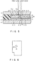
Light source 35 is an alignment beam source which emits white light H serving as an alignment beam. White light H emitted fromlight source 35 is converted byoptical lens 36 into a collimated white light beam having an increased diameter, and is then guided tobeam splitter 34. After being output frombeam splitter 34, laser beam Ra and white light beam H travel in the same optical path.Slit plate 37 is arranged in the optical path to which laser beam Ra and white light beam H output frombeam splitter 34 are directed. As is shown in Fig. 3,slit plate 37 hasring slit 38 formed therein. To be more specific,slit plate 37 is made up ofglass substrate 39, andmetal 40 which is coated onsubstrate 39 in such a manner as to formring slit 38. Normally, a plurality of slit plates respectively having ring slits of different diameters are prepared. - After passing through
ring slit 38 ofslit plate 37, laser beam Ra and white light beam H are guided to beam-focusingoptical system 41. This optical system converges both laser beam Ra and white light beam H and focuses them on the same portion ofliquid crystal display 21. More specifically, beam-focusingoptical system 41 is constituted by a microscope, which includesdichroic mirror 42 and converging lens 43 located in the optical path of the light reflected bydichroic mirror 42. Laser beam Ra and white light beam H are first reflected bydichroic mirror 42 and are then converged by converging lens 43. In the optical path connecting betweendichroic mirror 42 and converging lens 43,beam splitter 44 and focusinglens 45 are arranged in series.Illuminator 46 is arranged at a location branching frombeam splitter 44. Therefore, light P2 emitted fromilluminator 46 is first reflected bybeam splitter 44, and is then directed toliquid crystal display 21 throughdichroic mirror 42 and converging lens 43. The light reflected byliquid crystal display 21 passes through converging lens 43,dichroic mirror 42, andbeam splitter 44, and is guided to focusinglens 45. - An image sensor, for example, CCD (charge-coupled device)
camera 47 is located at the focal position of focusinglens 45, to pick up the image oflight crystal display 21 throughoptical system 41. Image signals output fromCCD camera 47 are supplied to monitortelevision set 48. - Driving
unit 49, used for positioning of beams, causes relative movement between XY table 20 and beam-focusingoptical system 41. By utilization of this relative movement, laser beam Ra and white light beam H output from beam-focusingoptical system 41 are positioned on a defective portion ofliquid crystal display 21 such that their beam rings surrounds the defective portion. The operator performs this operation while observing the beam rings throughmonitor television set 48. - A description may now be given of the repairing operation performed by use of the above-mentioned apparatus.
- After manufactured,
liquid crystal display 21 is inspected. If a defect caused by inclusion of foreign matter toliquid crystal display 21 is found in this inspection,liquid crystal display 21 is mounted on XY table 20 such that it is located under beam-focusingoptical system 41. In this condition,illuminator 46 emits light beam P2 tobeam splitter 44. This light beam is reflected bybeam splitter 44, passes through bothdichroic mirror 42 and converging lens 43, and then falls onliquid crystal display 21. At the time,CCD camera 47 image-picks upliquid crystal display 21 throughdichroic mirror 42,beam splitter 44 andbeamfocusing lens 45. The image signals output fromCCD camera 47 are supplied to monitortelevision set 48, which displays an image corresponding to the image signals. - In the meantime,
liquid crystal display 21 is irradiated with white light beam P1 emitted from back-light illumination unit 23 and is driven by liquid crystal display-drivingunit 24. - On
monitor television set 48, an image ofliquid crystal display 21 is displayed. In this state, XY table 20 is driven in the XY plane by drivingunit 49. - Therefore, different portions of
liquid crystal display 21 are sequentially shown onmonitor television set 48 in accordance with the movement of XY table 20. While observingliquid crystal display 21 shown onmonitor television set 48, the operator searches the defective portion ofliquid crystal display 21. When the location of the defective portion is detected,light source 35 is turned on, to thereby emit white light beam H used for alignment. White light beam H is converted into a collimated beam having a larger diameter, and is guided toslit plate 37 throughbeam splitter 34. When white light beam H passes through ring slit 38, it is defined as a ring-like white light beam. The ring-like white light beam is guided to beam-focusingoptical system 41. In this optical system, ring-like white light beam H is reflected bydichroic mirror 42, is converged by converging lens 43, and is made to fall onliquid crystal display 21.Liquid crystal display 21 mounted on XY table 20 is moved in the XY plane, with ring-like white light beam H falling thereon, until ring-like white light beam H surroundsforeign matter 50, as is shown in Fig. 4. It should be noted that the diameter of the ring-like white light beam falling onliquid crystal display 21 is determined byslit plate 37 to be employed. - When
foreign matter 50 is surrounded by ring-like white light beam H, laser beam R is output by laser oscillator 30. By optical lens system 32, laser beam R is converted into collimated laser beam Ra whose diameter is larger than that of laser beam R. Laser beam Ra is reflected by bothmirror 33 andbeam splitter 34, and is then guided toslit plate 37. When laser beam Ra passes through ring slit 38 ofslit plate 37, it is defined as a ring-like laser beam. Ring-like laser beam, thus obtained, is guided to beam-focusingoptical system 41. In this optical system, ring-like laser beam is reflected bydichroic mirror 42, is converged by converging lens 43, and is made to fall onliquid crystal display 21. The location on which ring-like laser beam falls is the same as that on which white light beam H falls. - The state in which ring-like laser beam falls on
liquid crystal display 21 is illustrated in Fig. 5 in an enlarged scale. As is shown in Fig. 5, ring-like laser beam is focused on pixel electrode 5-2 ofliquid crystal display 21. As a result,annular region 51 which is irradiated with ring-like laser beam is burnt away, in other words, removed from pixel electrode 5-2.Small region 52 located inside ofannular region 51 is electrically insulated from the region located outside ofannular region 52. Even when liquid crystal display-drivingunit 24 does not apply any voltage betweencommon electrode 4 and pixel electrode 5-2, a voltage is applied betweensmall region 52 of pixel electrode 5-2 andcommon electrode 4. Although white light P2 emitted from back-light illumination unit 23 towardliquid crystal display 21 passes throughsmall region 52 and its corresponding region of color filter 6-2, this does not causes any problem in practice, since the area ofregion 52 is very small; it is less than one tenth of the area of one pixel. - As mentioned above, an annular region surrounding that part of pixel electrode 5-2 which contacts
foreign matter 50 is removed in such a manner thatsmall region 52 is electrically insulated from the other regions. Therefore, even ifforeign matter 50 entersliquid crystal 9, it is possible to reduce the area of that portion of a pixel electrode which is made defective byforeign matter 50. Even a liquid crystal display which is regarded as defective due to inclusion of foreign matter can be repaired and used as a commercial product. Therefore, the manufacturing yield of liquid crystal displays can be improved. - The present invention is not limited to the embodiment mentioned above. It can be modified in various manners without departing from the spirit and scope of the invention. For instance, an annular region located around foreign matter can be removed by scanning it with
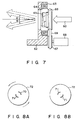
laser beam spot 60 in the direction indicated in Fig. 6. In this fashion as well, a portion which is short-circuited due to inclusion of foreign matter can be electrically insulated from the other portions. Whenlaser beam spot 60 is utilized, the scanning apparatus shown in Fig. 7 can be employed. As is shown in Fig. 7, the scanning apparatus compriseshousing 64 rotatably attached tobase 62 bybearings 63.Prism 65 is held byhousing 64.Pulley 66 is fixed tohousing 64, andmotor 68 is provided in the vicinity ofpulley 66.Pulley 67 is attached to the rotatable shaft ofmotor 68.Belt 69 is wound around pulleys 66 and 67. - In the apparatus shown in Fig. 7, the torque of
motor 68 is transmitted tohousing 64 throughbelt 69, so thatprism 65 is rotated by the torque. Thus,laser beam 60 is output fromprism 65, being refracted at angle ϑ. - By employing the apparatus shown in Fig. 7 in place of
slit plate 37,laser beam 60 can describe the track shown in Fig. 6. - In the above-mentioned embodiment, slit
plate 72 shown in Fig. 8 may be employed as a means for producing a ring-like beam. As is shown in Fig. 8, slitplate 72 has a pair of arcuate slits, each of which is about one fourth of a complete circle. During use, slitplate 72 is rotated 90° from the state shown in Fig. 8A to the state shown in Fig. 8B, to thereby produce a ring-like beam. - In the above-mentioned embodiment, white light beam H used as an alignment beam travels through the same optical path as that of the laser beam deflected by
beam splitter 34. However, white light beam H can be directed toliquid crystal display 21 through a different optical path to that of the laser beam.
Claims (10)
- A method of repairing a defective liquid crystal display of the type comprising a common electrode, pixel electrodes facing the common electrode, and a liquid crystal sealed between the common and pixel electrodes, the defect comprising conductive foreign matter which short-circuits the common electrode and a said pixel electrode to each other, said method characterized by comprising the step of:
irradiating the pixel electrode which is short-circuited to the common electrode with a laser beam such that at least a ring-like region of the said pixel electrode which corresponds to a ring line completely surrounding the portion of the pixel electrode which touches the foreign matter is removed by the laser beam, whereby the region of said pixel electrode inside of the ring line region is electrically isolated from the region of said pixel electrode outside of the ring line region. - An apparatus for repairing a liquid crystal display having a common electrode, a plurality of pixel electrodes facing the common electrode, and a liquid crystal sealed between the common and pixel electrides, the display having a defect comprising conductive foreign matter which short-circuits the common electrode and a said pixel electrode to each other, characterised by comprising:
laser oscillating means (30) for generating a laser beam;
alignment beam source means (35) for outputting an alignment beam used for alignment of the laser beam generated from said laser oscillating means;
first optical means (37) for shaping the laser beam and the alignment beam in such a manner that the laser beam and the alignment beam have a ring-shaped cross-section;
XY carriage means (20) on which the liquid crystal display is mounted and which is movable in an XY plane;
driving means (24) for driving the liquid crystal display;
second optical means (41) for focusing the laser beam and the alignment beam, the cross sections of which are ring-shaped, on a predetermined portion of the liquid crystal display;
illuminating means (46) for illuminating the liquid crystal display by directing light thereto through the second optical means;
image sensor means (47) picking an image of the liquid crystal display through the second optical means, to generate an image signal;
monitor means (48) for visualizing the image signal supplied from said image sensor means to allow detection of the said pixel electrode which is in contact with the foreign matter;
whereby a ring-like region of the pixel electrode which surrounds the electrode portion touching the foreign matter can be removed by the laser beam to electrically isolate the pixel electrode portion touching the foreign matter from the pixel electrode portion outside of said ring-like region. - An apparatus according to claim 2, characterized in that the alignment beam output from said alignment beam source means (35) is a white light beam.
- An apparatus according to claim 2, characterized in that said first optical means (37) comprises a slit plate, which includes a glass plate (39), and a metal layer (40) coated on the glass plate and having a ring slit corresponding to the ring-shaped cross-section.
- An apparatus according to claim 2, characterized in that said first optical means includes a plurality of slit plates which have different-diameter ring slits and are selectively employed.
- An apparatus according to claim 2, characterized in that said first optical means includes a prism (65) for refracting the laser beam at a predetermined angle, a rotatable housing (62) for holding the prism, a motor (68), and a belt (69) for transmitting torque of the motor to the housing.
- An apparatus according to claim 2, characterized in that said first optical means includes a slit plate (72) having an arcuate slit; and means for rotating the slit plate by a predetermined angle.
- An apparatus according to claim 2, characterized in that said XY carriage means is an XY table (20).
- An apparatus according to claim 2, characterized in that said first optical means includes a dichroic mirror (42) for reflecting the laser beam and the alignment beam guided from a slit plate, and a converging lens (43) for converging the laser beam and alignment beam reflected by the dichroic mirror.
- An apparatus according to claim 2, characterized in that said image sensor means includes a solidstate charge coupled device (47).
Applications Claiming Priority (4)
| Application Number | Priority Date | Filing Date | Title |
|---|---|---|---|
| JP27020388A JPH073625B2 (en) | 1988-10-26 | 1988-10-26 | How to fix LCD |
| JP270203/88 | 1988-10-26 | ||
| JP20475789A JPH0369914A (en) | 1989-08-09 | 1989-08-09 | Device for correcting liquid crystal display |
| JP204757/89 | 1989-08-09 |
Publications (3)
| Publication Number | Publication Date |
|---|---|
| EP0366459A2 EP0366459A2 (en) | 1990-05-02 |
| EP0366459A3 EP0366459A3 (en) | 1991-07-31 |
| EP0366459B1 true EP0366459B1 (en) | 1994-05-04 |
Family
ID=26514628
Family Applications (1)
| Application Number | Title | Priority Date | Filing Date |
|---|---|---|---|
| EP89311040A Expired - Lifetime EP0366459B1 (en) | 1988-10-26 | 1989-10-26 | Method of repairing liquid crystal display and apparatus using the method |
Country Status (3)
| Country | Link |
|---|---|
| US (1) | US5017755A (en) |
| EP (1) | EP0366459B1 (en) |
| DE (1) | DE68915115T2 (en) |
Families Citing this family (54)
| Publication number | Priority date | Publication date | Assignee | Title |
|---|---|---|---|---|
| DE4013195A1 (en) * | 1990-04-25 | 1991-10-31 | Lambda Physik Forschung | DEVICE AND METHOD FOR MONITORING THE PROCESSING OF A WORKPIECE WITH PULSED LASER RADIATION |
| JP3150322B2 (en) * | 1990-05-18 | 2001-03-26 | 株式会社日立製作所 | Wiring cutting method by laser and laser processing device |
| EP0458199B1 (en) * | 1990-05-21 | 1995-08-23 | Ntn Corporation | Laser processing device and laser processing method |
| US5285150A (en) * | 1990-11-26 | 1994-02-08 | Photon Dynamics, Inc. | Method and apparatus for testing LCD panel array |
| US5081687A (en) | 1990-11-30 | 1992-01-14 | Photon Dynamics, Inc. | Method and apparatus for testing LCD panel array prior to shorting bar removal |
| JPH04208834A (en) * | 1990-12-04 | 1992-07-30 | Ezel Inc | Method for inspecting liquid crystal panel |
| JP2766563B2 (en) * | 1991-03-27 | 1998-06-18 | シャープ株式会社 | Liquid crystal display |
| US5164565A (en) * | 1991-04-18 | 1992-11-17 | Photon Dynamics, Inc. | Laser-based system for material deposition and removal |
| US5168141A (en) * | 1991-06-14 | 1992-12-01 | General Electric Company | Vision guided laser welding |
| US5175504A (en) * | 1991-06-17 | 1992-12-29 | Photon Dynamics, Inc. | Method and apparatus for automatically inspecting and repairing a simple matrix circuit panel |
| US5235272A (en) * | 1991-06-17 | 1993-08-10 | Photon Dynamics, Inc. | Method and apparatus for automatically inspecting and repairing an active matrix LCD panel |
| US5432461A (en) * | 1991-06-28 | 1995-07-11 | Photon Dynamics, Inc. | Method of testing active matrix liquid crystal display substrates |
| US5459409A (en) * | 1991-09-10 | 1995-10-17 | Photon Dynamics, Inc. | Testing device for liquid crystal display base plate |
| US5504438A (en) * | 1991-09-10 | 1996-04-02 | Photon Dynamics, Inc. | Testing method for imaging defects in a liquid crystal display substrate |
| US5543729A (en) * | 1991-09-10 | 1996-08-06 | Photon Dynamics, Inc. | Testing apparatus and connector for liquid crystal display substrates |
| US5444385A (en) * | 1991-09-10 | 1995-08-22 | Photon Dynamics, Inc. | Testing apparatus for liquid crystal display substrates |
| US5465052A (en) * | 1991-09-10 | 1995-11-07 | Photon Dynamics, Inc. | Method of testing liquid crystal display substrates |
| US5241419A (en) * | 1992-01-27 | 1993-08-31 | General Electric Company | Co-axial viewing device for lasers |
| US5514850A (en) * | 1992-06-30 | 1996-05-07 | Sharp Kabushiki Kaisha | Defect compensation method for smoothing a surface of a transparent plate with an ArF excimer laser beam |
| JP3293136B2 (en) * | 1993-06-04 | 2002-06-17 | セイコーエプソン株式会社 | Laser processing apparatus and laser processing method |
| US5518956A (en) * | 1993-09-02 | 1996-05-21 | General Electric Company | Method of isolating vertical shorts in an electronic array using laser ablation |
| JP3179963B2 (en) * | 1994-04-26 | 2001-06-25 | 松下電器産業株式会社 | Laser processing device and laser processing method |
| US5932119A (en) * | 1996-01-05 | 1999-08-03 | Lazare Kaplan International, Inc. | Laser marking system |
| JP3292058B2 (en) | 1996-10-01 | 2002-06-17 | 三菱電機株式会社 | Method and apparatus for processing wiring substrate using laser light |
| JP3063688B2 (en) * | 1997-07-30 | 2000-07-12 | 日本電気株式会社 | Laser processing apparatus, control method therefor, and recording medium storing control program therefor |
| JP4659300B2 (en) * | 2000-09-13 | 2011-03-30 | 浜松ホトニクス株式会社 | Laser processing method and semiconductor chip manufacturing method |
| US6465767B2 (en) * | 2000-12-27 | 2002-10-15 | General Electric Company | Photomultiplier tube reprocessing |
| ATE534142T1 (en) | 2002-03-12 | 2011-12-15 | Hamamatsu Photonics Kk | METHOD FOR SEPARATING A SUBSTRATE |
| JP2005032576A (en) * | 2003-07-04 | 2005-02-03 | Fuji Electric Holdings Co Ltd | Restoration method and restoration device of polychromatic organic light emission display element |
| JP2005276600A (en) * | 2004-03-24 | 2005-10-06 | Hitachi Ltd | Manufacturing method of organic electroluminescent display device |
| JP4688525B2 (en) * | 2004-09-27 | 2011-05-25 | 株式会社 日立ディスプレイズ | Pattern correction device and display device manufacturing method |
| US7317325B2 (en) * | 2004-12-09 | 2008-01-08 | Applied Materials, Inc. | Line short localization in LCD pixel arrays |
| CN100353222C (en) * | 2005-02-21 | 2007-12-05 | 广辉电子股份有限公司 | Manufacture of panel of liquid crystal displaying device |
| GB0625001D0 (en) * | 2006-12-14 | 2007-01-24 | Plastic Logic Ltd | Short isolation |
| DE502008001155D1 (en) * | 2008-05-02 | 2010-09-30 | Leister Process Tech | Method and laser device for machining and / or connecting workpieces by means of laser radiation with power acting and pilot laser and at least one diffractive optical element |
| US10303035B2 (en) | 2009-12-22 | 2019-05-28 | View, Inc. | Self-contained EC IGU |
| US8164818B2 (en) | 2010-11-08 | 2012-04-24 | Soladigm, Inc. | Electrochromic window fabrication methods |
| US8643933B2 (en) | 2011-12-14 | 2014-02-04 | View, Inc. | Connectors for smart windows |
| US10180606B2 (en) | 2010-12-08 | 2019-01-15 | View, Inc. | Connectors for smart windows |
| US9454055B2 (en) | 2011-03-16 | 2016-09-27 | View, Inc. | Multipurpose controller for multistate windows |
| US10175549B2 (en) | 2011-03-16 | 2019-01-08 | View, Inc. | Connectors for smart windows |
| US9885934B2 (en) * | 2011-09-14 | 2018-02-06 | View, Inc. | Portable defect mitigators for electrochromic windows |
| WO2013039915A1 (en) | 2011-09-14 | 2013-03-21 | Soladigm, Inc. | Portable defect mitigator for electrochromic windows |
| US11719039B2 (en) | 2011-12-14 | 2023-08-08 | View, Inc. | Connectors for smart windows |
| EP3410183B1 (en) | 2012-03-13 | 2022-06-15 | View, Inc. | Visible defect mitigation for electrochromic windows |
| US9341912B2 (en) | 2012-03-13 | 2016-05-17 | View, Inc. | Multi-zone EC windows |
| US10583523B2 (en) | 2012-05-18 | 2020-03-10 | View, Inc. | Circumscribing defects in optical devices |
| US11255120B2 (en) | 2012-05-25 | 2022-02-22 | View, Inc. | Tester and electrical connectors for insulated glass units |
| EP3842613A1 (en) | 2012-08-23 | 2021-06-30 | View, Inc. | Photonic powered electrochromic devices |
| US9304090B2 (en) * | 2013-03-11 | 2016-04-05 | Electro Scientific Industries, Inc. | Systems and methods for providing polarization compensated multi-spectral laser repair of liquid crystal display panels |
| US9405254B2 (en) * | 2013-11-26 | 2016-08-02 | Xerox Corporation | Device for uniform light intensity generation |
| DE102014108259A1 (en) * | 2014-06-12 | 2015-12-17 | Scanlab Ag | Device for laser material processing |
| WO2018152249A1 (en) | 2017-02-16 | 2018-08-23 | View, Inc. | Solar power dynamic glass for heating and cooling buildings |
| CN112540471B (en) * | 2020-12-04 | 2021-11-23 | Tcl华星光电技术有限公司 | Display panel, lighting test method and lighting test device |
Family Cites Families (7)
| Publication number | Priority date | Publication date | Assignee | Title |
|---|---|---|---|---|
| US3947093A (en) * | 1973-06-28 | 1976-03-30 | Canon Kabushiki Kaisha | Optical device for producing a minute light beam |
| US3972599A (en) * | 1974-09-16 | 1976-08-03 | Caterpillar Tractor Co. | Method and apparatus for focussing laser beams |
| US4190759A (en) * | 1975-08-27 | 1980-02-26 | Hitachi, Ltd. | Processing of photomask |
| JPS5641088A (en) * | 1979-09-12 | 1981-04-17 | Hitachi Ltd | Monitoring device for laser light axis |
| JPH0774866B2 (en) * | 1982-10-06 | 1995-08-09 | セイコー電子工業株式会社 | Liquid crystal display manufacturing method |
| JPS60176022A (en) * | 1984-02-22 | 1985-09-10 | Sharp Corp | Manufacture of liquid crystal display element |
| JP2698357B2 (en) * | 1987-08-17 | 1998-01-19 | キヤノン株式会社 | Isolation method of short circuit between electrodes and manufacturing method of liquid crystal panel |
-
1989
- 1989-10-20 US US07/424,695 patent/US5017755A/en not_active Expired - Fee Related
- 1989-10-26 DE DE68915115T patent/DE68915115T2/en not_active Expired - Fee Related
- 1989-10-26 EP EP89311040A patent/EP0366459B1/en not_active Expired - Lifetime
Also Published As
| Publication number | Publication date |
|---|---|
| EP0366459A2 (en) | 1990-05-02 |
| EP0366459A3 (en) | 1991-07-31 |
| DE68915115T2 (en) | 1994-10-13 |
| US5017755A (en) | 1991-05-21 |
| DE68915115D1 (en) | 1994-06-09 |
Similar Documents
| Publication | Publication Date | Title |
|---|---|---|
| EP0366459B1 (en) | Method of repairing liquid crystal display and apparatus using the method | |
| US6639201B2 (en) | Spot grid array imaging system | |
| JP3199481B2 (en) | Inspection equipment for liquid crystal display substrates | |
| JPH0627479A (en) | Method and apparatus for automatic inspection and repair of simple matrix circuit panel | |
| JP6670561B2 (en) | Seamless fusion of telecentric brightfield and annular darkfield illumination | |
| EP1393115B1 (en) | Systems and methods for scanning a beam of light across a specimen | |
| KR20050107502A (en) | Microscope and sample observing method | |
| US4448527A (en) | Method and apparatus for detecting surface defects in mechanical workpieces | |
| KR930001517B1 (en) | Method and apparatus for joining together associated metal conductors of a layer structure with an insulating layer provided therebetween | |
| US20030117614A1 (en) | Method of inspecting optical waveguide substrate for optical conduction at increased speed and also inspecting optical waveguide substrate for crosstalk | |
| JPH0369914A (en) | Device for correcting liquid crystal display | |
| CN112098421A (en) | Dark field detection device | |
| JP3078102B2 (en) | Liquid crystal display repair method and device | |
| US20130208270A1 (en) | Defect inspecting apparatus and defect inspecting method | |
| JPH09210660A (en) | Image pick-up inspection system | |
| JPH06331945A (en) | Inspection instrument and defect correcting device for with display equipment | |
| JPH09201689A (en) | Focal position detector and laser beam machine using such a device | |
| JP2001264266A (en) | Substrate inspecting device | |
| EP0526734A2 (en) | Noncontact probe and active matrix array inspection apparatus using the same | |
| JPH0990233A (en) | Microscope | |
| JPH05288640A (en) | Inspection method for color filter | |
| JPH08304298A (en) | Infrared inspection system | |
| JPH04239149A (en) | Microscopic system for examination of crystal cleavage plane | |
| JP3776628B2 (en) | Inspection method using image processing apparatus | |
| KR0183700B1 (en) | Panel detecting apparatus of cathode ray tube |
Legal Events
| Date | Code | Title | Description |
|---|---|---|---|
| PUAI | Public reference made under article 153(3) epc to a published international application that has entered the european phase |
Free format text: ORIGINAL CODE: 0009012 |
|
| 17P | Request for examination filed |
Effective date: 19891116 |
|
| AK | Designated contracting states |
Kind code of ref document: A2 Designated state(s): DE FR NL |
|
| PUAL | Search report despatched |
Free format text: ORIGINAL CODE: 0009013 |
|
| AK | Designated contracting states |
Kind code of ref document: A3 Designated state(s): DE FR NL |
|
| 17Q | First examination report despatched |
Effective date: 19930308 |
|
| GRAA | (expected) grant |
Free format text: ORIGINAL CODE: 0009210 |
|
| AK | Designated contracting states |
Kind code of ref document: B1 Designated state(s): DE FR NL |
|
| REF | Corresponds to: |
Ref document number: 68915115 Country of ref document: DE Date of ref document: 19940609 |
|
| ET | Fr: translation filed | ||
| PLBE | No opposition filed within time limit |
Free format text: ORIGINAL CODE: 0009261 |
|
| STAA | Information on the status of an ep patent application or granted ep patent |
Free format text: STATUS: NO OPPOSITION FILED WITHIN TIME LIMIT |
|
| 26N | No opposition filed | ||
| PGFP | Annual fee paid to national office [announced via postgrant information from national office to epo] |
Ref country code: FR Payment date: 19961009 Year of fee payment: 8 |
|
| PGFP | Annual fee paid to national office [announced via postgrant information from national office to epo] |
Ref country code: DE Payment date: 19961104 Year of fee payment: 8 |
|
| PG25 | Lapsed in a contracting state [announced via postgrant information from national office to epo] |
Ref country code: FR Free format text: THE PATENT HAS BEEN ANNULLED BY A DECISION OF A NATIONAL AUTHORITY Effective date: 19971031 |
|
| PG25 | Lapsed in a contracting state [announced via postgrant information from national office to epo] |
Ref country code: DE Free format text: LAPSE BECAUSE OF NON-PAYMENT OF DUE FEES Effective date: 19980701 |
|
| REG | Reference to a national code |
Ref country code: FR Ref legal event code: ST |
|
| PGFP | Annual fee paid to national office [announced via postgrant information from national office to epo] |
Ref country code: NL Payment date: 19981028 Year of fee payment: 10 |
|
| PG25 | Lapsed in a contracting state [announced via postgrant information from national office to epo] |
Ref country code: NL Free format text: LAPSE BECAUSE OF NON-PAYMENT OF DUE FEES Effective date: 20000501 |
|
| NLV4 | Nl: lapsed or anulled due to non-payment of the annual fee |
Effective date: 20000501 |