EP0366027A2 - Wafer flood polishing - Google Patents
Wafer flood polishing Download PDFInfo
- Publication number
- EP0366027A2 EP0366027A2 EP89119566A EP89119566A EP0366027A2 EP 0366027 A2 EP0366027 A2 EP 0366027A2 EP 89119566 A EP89119566 A EP 89119566A EP 89119566 A EP89119566 A EP 89119566A EP 0366027 A2 EP0366027 A2 EP 0366027A2
- Authority
- EP
- European Patent Office
- Prior art keywords
- slurry
- polishing
- recited
- approximately
- polish
- Prior art date
- Legal status (The legal status is an assumption and is not a legal conclusion. Google has not performed a legal analysis and makes no representation as to the accuracy of the status listed.)
- Granted
Links
- 238000005498 polishing Methods 0.000 title claims abstract description 36
- 239000002002 slurry Substances 0.000 claims abstract description 55
- 235000012431 wafers Nutrition 0.000 claims abstract description 30
- VYPSYNLAJGMNEJ-UHFFFAOYSA-N Silicium dioxide Chemical compound O=[Si]=O VYPSYNLAJGMNEJ-UHFFFAOYSA-N 0.000 claims abstract description 18
- 239000012212 insulator Substances 0.000 claims abstract description 8
- 239000000377 silicon dioxide Substances 0.000 claims abstract description 6
- 229910052814 silicon oxide Inorganic materials 0.000 claims abstract description 3
- 238000000034 method Methods 0.000 claims description 36
- 230000008569 process Effects 0.000 claims description 23
- 239000000758 substrate Substances 0.000 claims description 12
- XUIMIQQOPSSXEZ-UHFFFAOYSA-N Silicon Chemical compound [Si] XUIMIQQOPSSXEZ-UHFFFAOYSA-N 0.000 claims description 11
- 229910052710 silicon Inorganic materials 0.000 claims description 11
- 239000010703 silicon Substances 0.000 claims description 11
- 235000019589 hardness Nutrition 0.000 claims description 8
- 239000004065 semiconductor Substances 0.000 claims description 7
- 239000007787 solid Substances 0.000 claims description 7
- 239000000463 material Substances 0.000 claims description 5
- 235000012239 silicon dioxide Nutrition 0.000 claims description 3
- 229910052681 coesite Inorganic materials 0.000 claims description 2
- 229910052906 cristobalite Inorganic materials 0.000 claims description 2
- 229910052682 stishovite Inorganic materials 0.000 claims description 2
- 229910052905 tridymite Inorganic materials 0.000 claims description 2
- 230000003028 elevating effect Effects 0.000 claims 2
- 239000006194 liquid suspension Substances 0.000 claims 1
- 239000000725 suspension Substances 0.000 claims 1
- 238000007517 polishing process Methods 0.000 abstract description 5
- 229910052581 Si3N4 Inorganic materials 0.000 abstract description 2
- HQVNEWCFYHHQES-UHFFFAOYSA-N silicon nitride Chemical compound N12[Si]34N5[Si]62N3[Si]51N64 HQVNEWCFYHHQES-UHFFFAOYSA-N 0.000 abstract description 2
- 238000002161 passivation Methods 0.000 description 9
- 239000002184 metal Substances 0.000 description 8
- 229910052751 metal Inorganic materials 0.000 description 8
- 238000006748 scratching Methods 0.000 description 5
- 230000002393 scratching effect Effects 0.000 description 5
- 238000009987 spinning Methods 0.000 description 5
- XLYOFNOQVPJJNP-UHFFFAOYSA-N water Chemical compound O XLYOFNOQVPJJNP-UHFFFAOYSA-N 0.000 description 5
- 230000003750 conditioning effect Effects 0.000 description 4
- 229920002120 photoresistant polymer Polymers 0.000 description 4
- 230000008901 benefit Effects 0.000 description 3
- 239000005380 borophosphosilicate glass Substances 0.000 description 3
- 238000001514 detection method Methods 0.000 description 3
- 238000002474 experimental method Methods 0.000 description 3
- PNEYBMLMFCGWSK-UHFFFAOYSA-N aluminium oxide Inorganic materials [O-2].[O-2].[O-2].[Al+3].[Al+3] PNEYBMLMFCGWSK-UHFFFAOYSA-N 0.000 description 2
- 239000008367 deionised water Substances 0.000 description 2
- 229910021641 deionized water Inorganic materials 0.000 description 2
- 230000001066 destructive effect Effects 0.000 description 2
- 239000005360 phosphosilicate glass Substances 0.000 description 2
- 238000007790 scraping Methods 0.000 description 2
- 238000012876 topography Methods 0.000 description 2
- 239000002253 acid Substances 0.000 description 1
- 150000007513 acids Chemical class 0.000 description 1
- 230000009471 action Effects 0.000 description 1
- 230000002411 adverse Effects 0.000 description 1
- 230000003466 anti-cipated effect Effects 0.000 description 1
- 239000000919 ceramic Substances 0.000 description 1
- 230000008859 change Effects 0.000 description 1
- 230000007423 decrease Effects 0.000 description 1
- 230000003247 decreasing effect Effects 0.000 description 1
- 238000002050 diffraction method Methods 0.000 description 1
- 230000008020 evaporation Effects 0.000 description 1
- 238000001704 evaporation Methods 0.000 description 1
- 230000010354 integration Effects 0.000 description 1
- 150000002500 ions Chemical class 0.000 description 1
- 230000001788 irregular Effects 0.000 description 1
- 238000004519 manufacturing process Methods 0.000 description 1
- 230000007246 mechanism Effects 0.000 description 1
- 150000002739 metals Chemical class 0.000 description 1
- 230000003287 optical effect Effects 0.000 description 1
- 239000002245 particle Substances 0.000 description 1
- 230000000737 periodic effect Effects 0.000 description 1
- 150000002978 peroxides Chemical class 0.000 description 1
- 210000002381 plasma Anatomy 0.000 description 1
- 229920000642 polymer Polymers 0.000 description 1
- 229920006254 polymer film Polymers 0.000 description 1
- 230000002035 prolonged effect Effects 0.000 description 1
- 230000001737 promoting effect Effects 0.000 description 1
- 239000000126 substance Substances 0.000 description 1
- 238000009736 wetting Methods 0.000 description 1
Images
Classifications
-
- H—ELECTRICITY
- H01—ELECTRIC ELEMENTS
- H01L—SEMICONDUCTOR DEVICES NOT COVERED BY CLASS H10
- H01L21/00—Processes or apparatus adapted for the manufacture or treatment of semiconductor or solid state devices or of parts thereof
- H01L21/02—Manufacture or treatment of semiconductor devices or of parts thereof
- H01L21/04—Manufacture or treatment of semiconductor devices or of parts thereof the devices having at least one potential-jump barrier or surface barrier, e.g. PN junction, depletion layer or carrier concentration layer
- H01L21/18—Manufacture or treatment of semiconductor devices or of parts thereof the devices having at least one potential-jump barrier or surface barrier, e.g. PN junction, depletion layer or carrier concentration layer the devices having semiconductor bodies comprising elements of Group IV of the Periodic System or AIIIBV compounds with or without impurities, e.g. doping materials
- H01L21/30—Treatment of semiconductor bodies using processes or apparatus not provided for in groups H01L21/20 - H01L21/26
- H01L21/31—Treatment of semiconductor bodies using processes or apparatus not provided for in groups H01L21/20 - H01L21/26 to form insulating layers thereon, e.g. for masking or by using photolithographic techniques; After treatment of these layers; Selection of materials for these layers
- H01L21/3105—After-treatment
- H01L21/31051—Planarisation of the insulating layers
- H01L21/31053—Planarisation of the insulating layers involving a dielectric removal step
-
- B—PERFORMING OPERATIONS; TRANSPORTING
- B24—GRINDING; POLISHING
- B24B—MACHINES, DEVICES, OR PROCESSES FOR GRINDING OR POLISHING; DRESSING OR CONDITIONING OF ABRADING SURFACES; FEEDING OF GRINDING, POLISHING, OR LAPPING AGENTS
- B24B37/00—Lapping machines or devices; Accessories
- B24B37/005—Control means for lapping machines or devices
- B24B37/013—Devices or means for detecting lapping completion
-
- B—PERFORMING OPERATIONS; TRANSPORTING
- B24—GRINDING; POLISHING
- B24B—MACHINES, DEVICES, OR PROCESSES FOR GRINDING OR POLISHING; DRESSING OR CONDITIONING OF ABRADING SURFACES; FEEDING OF GRINDING, POLISHING, OR LAPPING AGENTS
- B24B37/00—Lapping machines or devices; Accessories
- B24B37/005—Control means for lapping machines or devices
- B24B37/015—Temperature control
-
- B—PERFORMING OPERATIONS; TRANSPORTING
- B24—GRINDING; POLISHING
- B24B—MACHINES, DEVICES, OR PROCESSES FOR GRINDING OR POLISHING; DRESSING OR CONDITIONING OF ABRADING SURFACES; FEEDING OF GRINDING, POLISHING, OR LAPPING AGENTS
- B24B37/00—Lapping machines or devices; Accessories
- B24B37/04—Lapping machines or devices; Accessories designed for working plane surfaces
- B24B37/042—Lapping machines or devices; Accessories designed for working plane surfaces operating processes therefor
-
- B—PERFORMING OPERATIONS; TRANSPORTING
- B24—GRINDING; POLISHING
- B24B—MACHINES, DEVICES, OR PROCESSES FOR GRINDING OR POLISHING; DRESSING OR CONDITIONING OF ABRADING SURFACES; FEEDING OF GRINDING, POLISHING, OR LAPPING AGENTS
- B24B49/00—Measuring or gauging equipment for controlling the feed movement of the grinding tool or work; Arrangements of indicating or measuring equipment, e.g. for indicating the start of the grinding operation
- B24B49/16—Measuring or gauging equipment for controlling the feed movement of the grinding tool or work; Arrangements of indicating or measuring equipment, e.g. for indicating the start of the grinding operation taking regard of the load
Definitions
- passivated substrates are rotated against a polishing pad in the presence of an abrasive slurry.
- the slurry is pH-controlled such that the etch rate of the passivation layer can be controlled.
- U.S. Patent Application S.N. 791,860 entitled “Chem-Mech Polishing Method for Producing Co-Planar Metal/Insulator Films On a Substrate,” filed October 28, 1985, different slurry chemistries are used to optimize insulator-to-metal (or visa-versa) etch rate ratios to achieve a planar surface.
- the amount of slurry is kept to a minimum.
- the slurry is applied by a dropper suspended above the center of the polish wheel. As the wheel spins, the slurry is spread over the polish pad. Examples of low slurry content polishing are shown in U.S. Patent 3,841,031, entitled “Process for Polishing Thin Elements”; U.S. Patent 3,342,652, entitled “Chemical Polishing of A Semi-Conductor Substrate”; U.S. Patent 4,256,535, entitled “Method of Polishing a Semiconductor Wafer”; U.S. Patent 4,373,991, entitled “Method and Apparatus for Polishing A Semiconductor Wafer”; and an article entitled “Spinning Etchant Polishes Flat, Fast” Electronics , January 13, 1982, pp. 40-41.
- polish uniformity is in the range of 97%.
- pad lifetime is appreciably extended (up to 10X) because a less vigorous break-in procedure may now be used.
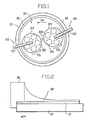
- the invention is carried out on a rotating polish wheel 10 having a circular polishing pad 12 mounted thereon.
- the polishing wheel 10 rotates in a direction indicated by arrow 14.
- the inventors have practiced the invention on a polish tool Model No. 6CU sold by the Strasbaugh Co. of Huntington Beach, CA.
- the wafers 28 to be planarized are held against the spinning polish wheel 10 by a quill assembly 20.
- the quill assembly includes a moveable support arm 22 for bringing the wafer 28 into contact with the polish pad 12, and a wafer support 24 that spins in a direction indicated by arrow 26.
- the wafer support 26 is rotated by a belt assembly (not shown) disposed within support arm 22.
- the support 24 has an elastomeric pad (not shown) disposed within it for receiving the wafer 28.
- the wafers 28 are polished by the action of the spinning support 24, the spinning pad 12, and the slurry pool 30 disposed therebetween.
- the spin speed of both the table 10 and the quill 20 is reduced from 120 RPM to 15-30 RPM.
- endpoint detection is facilitated.
- silicon is much less susceptible to polishing. This means that when the silicon surface rubs against the polish wheel, it produces a far greater amount of drag than does the oxide.
- the inventors have taken advantage of this phenomenon to provide an accurate endpoint detection method.
- a monitor (or dummy) wafer is included.
- the dummy wafer is a silicon substrate having the same amount of oxide on it as the amount of oxide on the product wafers to be removed by polishing.
- a pool of slurry is used in which the temperature is raised above room temperature, such that both polish rate uniformity and pad lifetime are maximized without promoting bumps.
Abstract
Description
- The invention relates to a method of planarizing workpieces utilizing an abrasive slurry in conjunction with a polishing pad.
- In the art of forming metallic interconnection layers on processed semiconductor substrates, it is known that various processing difficulties are presented if the primary passivation layer has an irregular topography. Such difficulties include unacceptable variations in metal layer thickness, which result in the possibility of undesired metal opens/shorts.
- At first, this problem was dealt with by using a passivation material (such as phosphosilicate glass (PSG) or boro-phosphosilicate glass (BPSG)) that could be melted (or reflowed) to smooth out the upper surface. While this solution was perfectly acceptable for the device densities of the day, recent advances in integration have forced workers in the art to consider other alternatives. One such alternative is the so-called "planarizing etch-back" procedure, in which a layer of conventional photosensitive polymer (or "photoresist") is spin-applied on top of the passivation layer. The photoresist presents a planar upper surface. Then using an etch technique that is non-selective between the photoresist and the passivation layer, the layers are simultaneously etched such that the planar upper surface of the photoresist is transferred to the underlaying passivation layer. Such etch processes include sputter etches and reactive ion etches (RIE) in CF₄-O₂ plasmas. For example, see U.S.P. 4,710,264. This alternative has not been widely accepted in the art because it is very difficult to accurately determine etch endpoint. Another alternative presently under consideration is the so-called "chem-mech polish" (CMP) process. In this process, passivated substrates are rotated against a polishing pad in the presence of an abrasive slurry. Typically the slurry is pH-controlled such that the etch rate of the passivation layer can be controlled. In U.S. Patent Application S.N. 791,860, entitled "Chem-Mech Polishing Method for Producing Co-Planar Metal/Insulator Films On a Substrate," filed October 28, 1985, different slurry chemistries are used to optimize insulator-to-metal (or visa-versa) etch rate ratios to achieve a planar surface. For example, using an abrasive pad at a pressure of 13.78-55.12x10³Pa (2-8 PSI), and a slurry of 0.06 micron alumina particles in deionized water, a 1:1 etch rate ratio of metal:insulator was achieved. The metal etch rate increased (and the oxide etch rate decreased) as different acids are used to lower the pH to 2.2. Alternatively, by increasing the pH to 11-11.5, the insulator removal rate increased relative to metal when using silica particulates at a concentration of 1-10 weight percent. In U.S. Patent Application S.N. 085,863, entitled "Via Filling and Planarizing Technique," filed August 17, 1987, an alumina/deionized water/hydrogen peroxide slurry was used utilizing a pressure of 68.9-82.68x10³ Pa (10-12 PSI) to provide a planarized tungsten-BPSG surface, such that filled vias and a planarized passivation layer were simultaneously formed. See also U.S.P. 4,702,792, in which a polymer film is chem-mech polished to define an image pattern.
- In the above chem-mech polishing art, the amount of slurry is kept to a minimum. Typically, the slurry is applied by a dropper suspended above the center of the polish wheel. As the wheel spins, the slurry is spread over the polish pad. Examples of low slurry content polishing are shown in U.S. Patent 3,841,031, entitled "Process for Polishing Thin Elements"; U.S. Patent 3,342,652, entitled "Chemical Polishing of A Semi-Conductor Substrate"; U.S. Patent 4,256,535, entitled "Method of Polishing a Semiconductor Wafer"; U.S. Patent 4,373,991, entitled "Method and Apparatus for Polishing A Semiconductor Wafer"; and an article entitled "Spinning Etchant Polishes Flat, Fast" Electronics, January 13, 1982, pp. 40-41.
- Use of low slurry content polishing leads to several difficulties. One difficulty is shortened polish pad "lifetime." Pad lifetime relates to the total number of wafers that can be polished by a given pad. As the pad wears out, both the removal rate of the polished material and the uniformity of removal across the wafer substantially degrade. Pad lifetime is determined by the hardness of the pad, the polish conditions, and the break-in / conditioning procedures. Typically, in order to provide sufficient wetting of a polishing pad used in conjunction with a small amount of slurry, the pad must undergo a destructive break-in procedure (e.g., high-pressure scraping using a blade), as well as periodic conditioning (lower pressure scraping). Such procedures substantially reduce pad lifetime, such that the overall process is more expensive due to the frequency of pad replacement.
- Another difficulty is the lack of removal rate uniformity across a given wafer. Using low slurry content processes, the inventors tried to optimize uniformity by changing the slurry content as well as varying the hardness of the pad. None of these changes appreciably enhanced uniformity.
- Yet another difficulty is the occurrence of "bumps." Bumps are areas along the substrate having locally incomplete polishing. Typically they occur over areas that cover steep topologies. For example, when polishing an oxide passivation layer on top of a gate electrode, if the electrode provides a steep "step" (i.e., if it has a height more than approximately 0.5 microns), bumps will tend to form on the portion of the oxide above the edges of the electrode. In low slurry content applications, bumps cannot be eliminated without adversely affecting some other parameter (e.g., rate uniformity, pad life) that needs to be optimized.
- Accordingly, there is a need in the art for a planarization process in which both pad lifetime and polish rate uniformity can be maximized while simultaneously minimizing the occurrence of bumps. It is thus an object of the invention to provide a chem-mech planarization process that maximizes both pad lifetime and planarization uniformity.
- It is another object of the invention to optimize the above parameters while simultaneously minimizing the occurrence of bumps.
- It is yet another object of the invention to provide a chem-mech polishing process wherein the need to selectively introduce different slurries is eliminated.
- The above and other objects have been met by arranging a retaining wall about the polishing table, and introducing a pool of slurry that completely immerses the polish pad. Moreover, the slurry temperature is raised above room temperature.
- By utilizing a polishing process under the above conditions, polish uniformity is in the range of 97%. At the same time, pad lifetime is appreciably extended (up to 10X) because a less vigorous break-in procedure may now be used. Finally, these enhancements do not come at the expense of increased occurrence of bumps; rather, bumps are eliminated.
- The above and other aspects of the invention will be described in more detail below. In the description to follow, reference will be made to the accompanying Drawing, in which:
- Fig. 1 is a top view of the polishing apparatus of the invention; and
- Fig. 2 is a cross-sectional view of the polishing apparatus of the invention.
- With reference to Figs. 1 and 2, the invention is carried out on a rotating
polish wheel 10 having acircular polishing pad 12 mounted thereon. The polishingwheel 10 rotates in a direction indicated byarrow 14. There are a number of commercial polish wheels upon which the invention can be carried out. The inventors have practiced the invention on a polish tool Model No. 6CU sold by the Strasbaugh Co. of Huntington Beach, CA. - Disposed about the periphery of
polish wheel 10 is a retaining wall (or dam) 16. The purpose of thedam 16 is to increase the amount ofslurry 30 provided to thepolish pad 12, to the point where a slurry "pool" 30 is formed which is sufficient to completely cover thepad 12 even when it is spinning during the polishing process. See Namba et al, "Ultrafine Finishing of Ceramics and Metals by Float Polishing." Laser Induced Damage in Optical Materials" Conference Proceedings 1980, pgs. 171-179. See also U.S. Patent 2,922,264. In the present invention, the dam is 5.1 cm (two inches) high, such that a slurry pool approximately 0.63 cm (1/4 inch) deep is formed covering thepolish pad 12. - The
wafers 28 to be planarized are held against the spinningpolish wheel 10 by aquill assembly 20. The quill assembly includes amoveable support arm 22 for bringing thewafer 28 into contact with thepolish pad 12, and awafer support 24 that spins in a direction indicated byarrow 26. Note that thewafer support 26 is rotated by a belt assembly (not shown) disposed withinsupport arm 22. Thesupport 24 has an elastomeric pad (not shown) disposed within it for receiving thewafer 28. Thus, thewafers 28 are polished by the action of the spinningsupport 24, thespinning pad 12, and theslurry pool 30 disposed therebetween. - When utilizing large slurry amounts, the inventors have found that both greater uniformity and prolonged pad life results. Specifically, under these conditions polish uniformity across the surface of a wafer can be as high as 97%. At the same time, polish pad lifetime is increased because a less vigorous break-in procedure can be used. Specifically, break-in can now be performed by polishing a number of blank wafers having an exposed coarse film thereon for a relatively short amount of time (e.g. five minutes). The amount of wafers is a function of polish pad hardness (the harder the pad, the less break-in is needed). For a very hard polish pad (e.g., the IC-40 pad sold by Rodel Corp. of Scottsdale, AZ), no break-in is necessary in this process.
- In carrying out experiments utilizing the polish apparatus discussed above, the inventors found that the temperature of the slurry plays a significant role in polish uniformity. Specifically, by raising the slurry temperature from room temperature to 29.4-35.0°C 85-95°F), the uniformity of the planarization etch was greatly improved, by up to a factor of two in some experiments. These findings were not anticipated, particularly in polishing layers such as oxides where the process is predominantly mechanical in nature. Moreover, after this phenomena was uncovered, the inventors expected that it would hold (and even increase) as a function of increased temperature. However, the inventors found that at temperatures above approximately 35.0-37.8°C (95-100°F), uniformity substantially degrades. The inventors postulate that at these higher temperatures, non-uniformity increases because it is very difficult to maintain constant slurry concentration due to evaporation. In other words, above approximately 37.8°C (100°F), increases in polish uniformity are negated by slurry non-uniformity.
- The inventors have found that the percentage of particulates in the slurry plays a role in the overall process. Specifically, the inventors found that when utilizing a pool of silica slurry, the polishing rate of the substrates increases (and the occurrence of bumps decreases) linearly with increasing solids percentage up to 10%. Above 10%, both polish rate and polish rate uniformity stay essentially constant, and bumps are at a minimum. Experiments indicate that above approximately 15 weight percent solids, polish rate uniformity degrades. When polishing in the presence of a small amount of slurry, both polish rate and polish rate non-uniformity increase with increasing solids percent. In other words, there is no appreciable operating "window" within which both polish rate and polish rate uniformity can be maximized by percent solids.
- The size of particulates also plays a role in the overall process. The inventors thought bumps were caused by small non-uniformities in the particulate concentration within the slurry. They tried to eliminate bumps by using a slurry having small (0.006 micron average size) particulates, on the assumption that smaller particulates would enhance the effective particulate concentration. Bumps continue to occur. When the size of the particulates was increased to 0.02 microns, bumps were eliminated. These results were achieved at removal rates between approximately 50 and 150 nm per minute. Above approximately 200 nm per minute, bumps could not be eliminated. Note that this removal rate limit is for blanket layers; in practice, when planarizing passivation layers overlaying steep topographies, localized removal rates of up to 600 nm per minute have been achieved without bumps.
- Moreover, by utilizing a pool of slurry, large particulates can be used for all polish applications, including those in which slurries having fine particulates are ordinarily used. In the invention, the slurry has been diluted in water to 12% (by weight) SiO₂ particulates (average diameter of 0.02 microns) suspended in water. The slurry is sold under the trade name "Cab-O-Sperse SC1" by Cabot Corp. Normally, a slurry having much smaller particulates would be used in situations in which only a small amount of material is to be polished away, and/or the underlaying surface is particularly sensitive to scratching (e.g., in polishing a thin silicon dioxide layer atop a polish-stop layer formed on a silicon substrate, we wish to avoid dislocations in the silicon crystallography that can result from scratching the silicon surface). The inventors found that by utilizing a pool of slurry at an elevated temperature, the mechanism by which particulate size contributes to scratching is eliminated. Thus, under these conditions scratching becomes a sole function of pad hardness (the harder the pad, the more scratches). In low slurry applications, softer pads could not be used because bumps would occur; this problem could only be alleviated by utilizing the destructive pad break-in/conditioning procedures previously discussed. Here, one can use a softer pad without producing bumps and without utilizing such pad break-in / conditioning procedures. Thus, the same coarse slurry can now be used in conventional fine slurry applications, reducing expense by eliminating the need to change slurries as a function of coarse/fine application.
- Further, in utilizing a pool of slurry, the spin speed of both the table 10 and the
quill 20 is reduced from 120 RPM to 15-30 RPM. Under these conditions, endpoint detection is facilitated. For example, when polishing oxide on a silicon wafer, it has been observed that silicon is much less susceptible to polishing. This means that when the silicon surface rubs against the polish wheel, it produces a far greater amount of drag than does the oxide. The inventors have taken advantage of this phenomenon to provide an accurate endpoint detection method. When multiple wafers are being polished, a monitor (or dummy) wafer is included. The dummy wafer is a silicon substrate having the same amount of oxide on it as the amount of oxide on the product wafers to be removed by polishing. Once the oxide is removed form the dummy wafer, the exposed silicon surface provides a large amount of drag. This maximum drag can be detected with a quill motor current detector. The motor controller is set to allow the quill to slow down at maximum drag. The controller senses that the motor rotation speed is too low and the motor current increases sharply, producing a current "spike." Thus, process endpoint is signaled by current spikes in the motor that turns the quill. - The above technique is applied to lower quill spin speeds, because at higher speeds the increased drag is less pronounced due to the increased angular momentum of the wafer. The invention will now be discussed with reference to Example 1 below:
- Purpose: To planarize a step height of approximately 800 nm of undoped oxide passivating a processed silicon substrate.
slurry: Cab-O-Sperse SC1, diluted in water to 12 weight percent
quill spin speed: 17 RPM
quill pressure: 62.01x10³Pa (9 PSI)
polish pad: Rodel Suba 500
polish wheel spin speed: 17 RPM
slurry temperature: 32.2°C (90°F)
number of wafers: 9, plus endpoint detection wafer
Results: After 7 minutes, oxide is completely planarized on the silicon surface, without bumps or scratching. - Thus, in the invention, a pool of slurry is used in which the temperature is raised above room temperature, such that both polish rate uniformity and pad lifetime are maximized without promoting bumps. These advantages of the invention can be realized whenever insulators such as silicon oxide or silicon nitride are to be polished. Moreover, the advantages of the invention are not limited to thc best mode embodiment described above; for example, other particulates having hardnesses commensurate with the hardness of the insulator to be polished can be used.
Claims (10)
providing sufficient slurry to form a pool defined by a dam disposed about the outer periphery of the polish wheel, wherein said polishing pad is immersed in said pool during polishing, and wherein said slurry comprises a liquid suspension of solid particulates having a hardness commensurate to the hardness of the insulator layer; and
elevating the temperature of said slurry to at least approximately 29.4°C (85°F).
15 RPM-20 RPM.
providing an amount of slurry sufficient to form a pool defined by a dam disposed about the polish wheel, wherein said polishing pad is immersed in said pool during polishing, and wherein said slurry comprises a suspension of 10%-15% silica particulates by weight, said particulates having an average diameter of at least approximately 0.02 microns; and
elevating the temperature of said slurry to at least approximately 29.4°C (85°F);
and wherein said polish wheel rotates at a speed no greater than approximately 30 RPM.
Applications Claiming Priority (2)
| Application Number | Priority Date | Filing Date | Title |
|---|---|---|---|
| US07/263,842 US4910155A (en) | 1988-10-28 | 1988-10-28 | Wafer flood polishing |
| US263842 | 1988-10-28 |
Publications (3)
| Publication Number | Publication Date |
|---|---|
| EP0366027A2 true EP0366027A2 (en) | 1990-05-02 |
| EP0366027A3 EP0366027A3 (en) | 1991-01-09 |
| EP0366027B1 EP0366027B1 (en) | 1993-09-15 |
Family
ID=23003463
Family Applications (1)
| Application Number | Title | Priority Date | Filing Date |
|---|---|---|---|
| EP89119566A Expired - Lifetime EP0366027B1 (en) | 1988-10-28 | 1989-10-21 | Wafer flood polishing |
Country Status (4)
| Country | Link |
|---|---|
| US (2) | US4910155A (en) |
| EP (1) | EP0366027B1 (en) |
| JP (1) | JPH077755B2 (en) |
| DE (1) | DE68909168T2 (en) |
Cited By (8)
| Publication number | Priority date | Publication date | Assignee | Title |
|---|---|---|---|---|
| DE4105145A1 (en) * | 1990-03-01 | 1991-09-05 | Intel Corp | METHOD AND DEVICE FOR PLANAR GRINDING THE SURFACE OF A DIELECTRIC APPLIED ON A SEMICONDUCTOR SUBSTRATE |
| EP0589434A1 (en) * | 1992-09-24 | 1994-03-30 | Ebara Corporation | Polishing apparatus |
| EP0624432A1 (en) * | 1992-10-30 | 1994-11-17 | Bbf Yamate Corporation | Polishing method, apparatus for the same and buff polishing wheel |
| EP0739686A2 (en) * | 1995-04-25 | 1996-10-30 | AT&T IPM Corp. | Method and apparatus for polishing metal-soluble materials such as diamond |
| EP0751205A2 (en) | 1995-06-29 | 1997-01-02 | Shell Internationale Researchmaatschappij B.V. | Process for converting residual hydrocarbon oils |
| WO1997044160A1 (en) * | 1996-05-21 | 1997-11-27 | Micron Technology, Inc. | Method for chemical-mechanical planarization of stop-on-feature semiconductor wafers |
| US5957750A (en) * | 1997-12-18 | 1999-09-28 | Micron Technology, Inc. | Method and apparatus for controlling a temperature of a polishing pad used in planarizing substrates |
| KR100359070B1 (en) * | 1998-10-13 | 2002-11-04 | 닛본 덴기 가부시끼가이샤 | Method of fabricating a semiconductor device |
Families Citing this family (147)
| Publication number | Priority date | Publication date | Assignee | Title |
|---|---|---|---|---|
| US5399528A (en) * | 1989-06-01 | 1995-03-21 | Leibovitz; Jacques | Multi-layer fabrication in integrated circuit systems |
| US5191738A (en) * | 1989-06-16 | 1993-03-09 | Shin-Etsu Handotai Co., Ltd. | Method of polishing semiconductor wafer |
| US5094972A (en) * | 1990-06-14 | 1992-03-10 | National Semiconductor Corp. | Means of planarizing integrated circuits with fully recessed isolation dielectric |
| US5036015A (en) * | 1990-09-24 | 1991-07-30 | Micron Technology, Inc. | Method of endpoint detection during chemical/mechanical planarization of semiconductor wafers |
| US5064683A (en) * | 1990-10-29 | 1991-11-12 | Motorola, Inc. | Method for polish planarizing a semiconductor substrate by using a boron nitride polish stop |
| US5413966A (en) * | 1990-12-20 | 1995-05-09 | Lsi Logic Corporation | Shallow trench etch |
| US5290396A (en) * | 1991-06-06 | 1994-03-01 | Lsi Logic Corporation | Trench planarization techniques |
| JP3362397B2 (en) * | 1991-03-28 | 2003-01-07 | ソニー株式会社 | Manufacturing method of electronic device including polishing step by polishing |
| US5069002A (en) * | 1991-04-17 | 1991-12-03 | Micron Technology, Inc. | Apparatus for endpoint detection during mechanical planarization of semiconductor wafers |
| US5128281A (en) * | 1991-06-05 | 1992-07-07 | Texas Instruments Incorporated | Method for polishing semiconductor wafer edges |
| US5252503A (en) * | 1991-06-06 | 1993-10-12 | Lsi Logic Corporation | Techniques for forming isolation structures |
| US5225358A (en) * | 1991-06-06 | 1993-07-06 | Lsi Logic Corporation | Method of forming late isolation with polishing |
| US5248625A (en) * | 1991-06-06 | 1993-09-28 | Lsi Logic Corporation | Techniques for forming isolation structures |
| US5320706A (en) * | 1991-10-15 | 1994-06-14 | Texas Instruments Incorporated | Removing slurry residue from semiconductor wafer planarization |
| US5308438A (en) * | 1992-01-30 | 1994-05-03 | International Business Machines Corporation | Endpoint detection apparatus and method for chemical/mechanical polishing |
| US5245790A (en) * | 1992-02-14 | 1993-09-21 | Lsi Logic Corporation | Ultrasonic energy enhanced chemi-mechanical polishing of silicon wafers |
| US5422289A (en) * | 1992-04-27 | 1995-06-06 | National Semiconductor Corporation | Method of manufacturing a fully planarized MOSFET and resulting structure |
| US5302551A (en) * | 1992-05-11 | 1994-04-12 | National Semiconductor Corporation | Method for planarizing the surface of an integrated circuit over a metal interconnect layer |
| US5445996A (en) * | 1992-05-26 | 1995-08-29 | Kabushiki Kaisha Toshiba | Method for planarizing a semiconductor device having a amorphous layer |
| JPH0697132A (en) * | 1992-07-10 | 1994-04-08 | Lsi Logic Corp | Mechanochemical polishing apparatus of semiconductor wafer, mounting method of semiconductor-wafer polishing pad to platen of above apparatus and polishing composite pad of above apparatus |
| US5265378A (en) * | 1992-07-10 | 1993-11-30 | Lsi Logic Corporation | Detecting the endpoint of chem-mech polishing and resulting semiconductor device |
| US5310455A (en) * | 1992-07-10 | 1994-05-10 | Lsi Logic Corporation | Techniques for assembling polishing pads for chemi-mechanical polishing of silicon wafers |
| US5299393A (en) * | 1992-07-21 | 1994-04-05 | International Business Machines Corporation | Slurry containment device for polishing semiconductor wafers |
| US5466636A (en) * | 1992-09-17 | 1995-11-14 | International Business Machines Corporation | Method of forming borderless contacts using a removable mandrel |
| US5529936A (en) * | 1992-09-30 | 1996-06-25 | Lsi Logic Corporation | Method of etching a lens for a semiconductor solid state image sensor |
| US5340978A (en) * | 1992-09-30 | 1994-08-23 | Lsi Logic Corporation | Image-sensing display panels with LCD display panel and photosensitive element array |
| US5760834A (en) * | 1992-09-30 | 1998-06-02 | Lsi Logic | Electronic camera with binary lens element array |
| US5232875A (en) * | 1992-10-15 | 1993-08-03 | Micron Technology, Inc. | Method and apparatus for improving planarity of chemical-mechanical planarization operations |
| US5300155A (en) * | 1992-12-23 | 1994-04-05 | Micron Semiconductor, Inc. | IC chemical mechanical planarization process incorporating slurry temperature control |
| US5324690A (en) * | 1993-02-01 | 1994-06-28 | Motorola Inc. | Semiconductor device having a ternary boron nitride film and a method for forming the same |
| US5626715A (en) * | 1993-02-05 | 1997-05-06 | Lsi Logic Corporation | Methods of polishing semiconductor substrates |
| US5389194A (en) * | 1993-02-05 | 1995-02-14 | Lsi Logic Corporation | Methods of cleaning semiconductor substrates after polishing |
| US5532191A (en) * | 1993-03-26 | 1996-07-02 | Kawasaki Steel Corporation | Method of chemical mechanical polishing planarization of an insulating film using an etching stop |
| US5356513A (en) * | 1993-04-22 | 1994-10-18 | International Business Machines Corporation | Polishstop planarization method and structure |
| DE69409655T2 (en) * | 1993-09-17 | 1998-08-06 | Polaroid Corp | MANUFACTURE OF MICRO LENSES ON SOLID IMAGE RECORDERS |
| US5395801A (en) * | 1993-09-29 | 1995-03-07 | Micron Semiconductor, Inc. | Chemical-mechanical polishing processes of planarizing insulating layers |
| US5643053A (en) * | 1993-12-27 | 1997-07-01 | Applied Materials, Inc. | Chemical mechanical polishing apparatus with improved polishing control |
| US5595522A (en) * | 1994-01-04 | 1997-01-21 | Texas Instruments Incorporated | Semiconductor wafer edge polishing system and method |
| US5422316A (en) * | 1994-03-18 | 1995-06-06 | Memc Electronic Materials, Inc. | Semiconductor wafer polisher and method |
| US5733175A (en) | 1994-04-25 | 1998-03-31 | Leach; Michael A. | Polishing a workpiece using equal velocity at all points overlapping a polisher |
| US5562530A (en) * | 1994-08-02 | 1996-10-08 | Sematech, Inc. | Pulsed-force chemical mechanical polishing |
| US5783497A (en) * | 1994-08-02 | 1998-07-21 | Sematech, Inc. | Forced-flow wafer polisher |
| US5607341A (en) | 1994-08-08 | 1997-03-04 | Leach; Michael A. | Method and structure for polishing a wafer during manufacture of integrated circuits |
| TW274625B (en) * | 1994-09-30 | 1996-04-21 | Hitachi Seisakusyo Kk | |
| US5527423A (en) * | 1994-10-06 | 1996-06-18 | Cabot Corporation | Chemical mechanical polishing slurry for metal layers |
| JP3637977B2 (en) * | 1995-01-19 | 2005-04-13 | 株式会社荏原製作所 | Polishing end point detection method |
| US5665201A (en) * | 1995-06-06 | 1997-09-09 | Advanced Micro Devices, Inc. | High removal rate chemical-mechanical polishing |
| KR970018240A (en) * | 1995-09-08 | 1997-04-30 | 모리시다 요이치 | Method and apparatus for polishing a semiconductor substrate |
| US5672095A (en) * | 1995-09-29 | 1997-09-30 | Intel Corporation | Elimination of pad conditioning in a chemical mechanical polishing process |
| US5840623A (en) * | 1995-10-04 | 1998-11-24 | Advanced Micro Devices, Inc. | Efficient and economical method of planarization of multilevel metallization structures in integrated circuits using CMP |
| US5709593A (en) * | 1995-10-27 | 1998-01-20 | Applied Materials, Inc. | Apparatus and method for distribution of slurry in a chemical mechanical polishing system |
| JP3649493B2 (en) * | 1995-11-02 | 2005-05-18 | 株式会社荏原製作所 | Polishing end point determination method and apparatus |
| US5726099A (en) * | 1995-11-07 | 1998-03-10 | International Business Machines Corporation | Method of chemically mechanically polishing an electronic component using a non-selective ammonium persulfate slurry |
| EP0779655A3 (en) * | 1995-12-14 | 1997-07-16 | International Business Machines Corporation | A method of chemically-mechanically polishing an electronic component |
| US5707492A (en) * | 1995-12-18 | 1998-01-13 | Motorola, Inc. | Metallized pad polishing process |
| US5618447A (en) * | 1996-02-13 | 1997-04-08 | Micron Technology, Inc. | Polishing pad counter meter and method for real-time control of the polishing rate in chemical-mechanical polishing of semiconductor wafers |
| KR0183826B1 (en) * | 1996-03-04 | 1999-05-01 | 김광호 | Cleaner and its cleaning method |
| JPH09321001A (en) * | 1996-05-31 | 1997-12-12 | Komatsu Electron Metals Co Ltd | Method for polishing semiconductor wafer |
| US5993686A (en) * | 1996-06-06 | 1999-11-30 | Cabot Corporation | Fluoride additive containing chemical mechanical polishing slurry and method for use of same |
| US5710069A (en) * | 1996-08-26 | 1998-01-20 | Motorola, Inc. | Measuring slurry particle size during substrate polishing |
| US5783489A (en) * | 1996-09-24 | 1998-07-21 | Cabot Corporation | Multi-oxidizer slurry for chemical mechanical polishing |
| US6033596A (en) * | 1996-09-24 | 2000-03-07 | Cabot Corporation | Multi-oxidizer slurry for chemical mechanical polishing |
| US6039891A (en) * | 1996-09-24 | 2000-03-21 | Cabot Corporation | Multi-oxidizer precursor for chemical mechanical polishing |
| JP3788533B2 (en) * | 1996-09-30 | 2006-06-21 | 東京エレクトロン株式会社 | Polishing apparatus and polishing method |
| US5972792A (en) * | 1996-10-18 | 1999-10-26 | Micron Technology, Inc. | Method for chemical-mechanical planarization of a substrate on a fixed-abrasive polishing pad |
| US6043206A (en) | 1996-10-19 | 2000-03-28 | Samsung Electronics Co., Ltd. | Solutions for cleaning integrated circuit substrates |
| US6068787A (en) * | 1996-11-26 | 2000-05-30 | Cabot Corporation | Composition and slurry useful for metal CMP |
| US5958288A (en) * | 1996-11-26 | 1999-09-28 | Cabot Corporation | Composition and slurry useful for metal CMP |
| US6126853A (en) * | 1996-12-09 | 2000-10-03 | Cabot Microelectronics Corporation | Chemical mechanical polishing slurry useful for copper substrates |
| US6309560B1 (en) | 1996-12-09 | 2001-10-30 | Cabot Microelectronics Corporation | Chemical mechanical polishing slurry useful for copper substrates |
| US5954997A (en) | 1996-12-09 | 1999-09-21 | Cabot Corporation | Chemical mechanical polishing slurry useful for copper substrates |
| US6602439B1 (en) * | 1997-02-24 | 2003-08-05 | Superior Micropowders, Llc | Chemical-mechanical planarization slurries and powders and methods for using same |
| US5885135A (en) * | 1997-04-23 | 1999-03-23 | International Business Machines Corporation | CMP wafer carrier for preferential polishing of a wafer |
| US5873769A (en) * | 1997-05-30 | 1999-02-23 | Industrial Technology Research Institute | Temperature compensated chemical mechanical polishing to achieve uniform removal rates |
| US6030487A (en) * | 1997-06-19 | 2000-02-29 | International Business Machines Corporation | Wafer carrier assembly |
| US6290735B1 (en) | 1997-10-31 | 2001-09-18 | Nanogram Corporation | Abrasive particles for surface polishing |
| US6726990B1 (en) | 1998-05-27 | 2004-04-27 | Nanogram Corporation | Silicon oxide particles |
| US20090075083A1 (en) * | 1997-07-21 | 2009-03-19 | Nanogram Corporation | Nanoparticle production and corresponding structures |
| US20060147369A1 (en) * | 1997-07-21 | 2006-07-06 | Neophotonics Corporation | Nanoparticle production and corresponding structures |
| US6099798A (en) * | 1997-10-31 | 2000-08-08 | Nanogram Corp. | Ultraviolet light block and photocatalytic materials |
| US20090255189A1 (en) * | 1998-08-19 | 2009-10-15 | Nanogram Corporation | Aluminum oxide particles |
| US7384680B2 (en) * | 1997-07-21 | 2008-06-10 | Nanogram Corporation | Nanoparticle-based power coatings and corresponding structures |
| US5997392A (en) * | 1997-07-22 | 1999-12-07 | International Business Machines Corporation | Slurry injection technique for chemical-mechanical polishing |
| US6099604A (en) | 1997-08-21 | 2000-08-08 | Micron Technology, Inc. | Slurry with chelating agent for chemical-mechanical polishing of a semiconductor wafer and methods related thereto |
| US6069095A (en) * | 1997-08-22 | 2000-05-30 | Texas Instruments Incorporated | Ultra-clean wafer chuck assembly for moisture-sensitive processes conducted in rapid thermal processors |
| US6102784A (en) * | 1997-11-05 | 2000-08-15 | Speedfam-Ipec Corporation | Method and apparatus for improved gear cleaning assembly in polishing machines |
| US6146241A (en) * | 1997-11-12 | 2000-11-14 | Fujitsu Limited | Apparatus for uniform chemical mechanical polishing by intermittent lifting and reversible rotation |
| US6336845B1 (en) | 1997-11-12 | 2002-01-08 | Lam Research Corporation | Method and apparatus for polishing semiconductor wafers |
| KR100286980B1 (en) * | 1998-02-11 | 2001-04-16 | 윤종용 | Method and apparatus for grinding wafers |
| US6114249A (en) * | 1998-03-10 | 2000-09-05 | International Business Machines Corporation | Chemical mechanical polishing of multiple material substrates and slurry having improved selectivity |
| US6432828B2 (en) | 1998-03-18 | 2002-08-13 | Cabot Microelectronics Corporation | Chemical mechanical polishing slurry useful for copper substrates |
| WO1999056189A1 (en) * | 1998-04-30 | 1999-11-04 | The Boc Group, Inc. | Conductivity feedback control system for slurry blending |
| US6019665A (en) * | 1998-04-30 | 2000-02-01 | Fujitsu Limited | Controlled retention of slurry in chemical mechanical polishing |
| US6210257B1 (en) * | 1998-05-29 | 2001-04-03 | Micron Technology, Inc. | Web-format polishing pads and methods for manufacturing and using web-format polishing pads in mechanical and chemical-mechanical planarization of microelectronic substrates |
| US5944588A (en) * | 1998-06-25 | 1999-08-31 | International Business Machines Corporation | Chemical mechanical polisher |
| US6217416B1 (en) | 1998-06-26 | 2001-04-17 | Cabot Microelectronics Corporation | Chemical mechanical polishing slurry useful for copper/tantalum substrates |
| US6063306A (en) * | 1998-06-26 | 2000-05-16 | Cabot Corporation | Chemical mechanical polishing slurry useful for copper/tantalum substrate |
| US6558570B2 (en) | 1998-07-01 | 2003-05-06 | Micron Technology, Inc. | Polishing slurry and method for chemical-mechanical polishing |
| US6220934B1 (en) * | 1998-07-23 | 2001-04-24 | Micron Technology, Inc. | Method for controlling pH during planarization and cleaning of microelectronic substrates |
| US6129610A (en) * | 1998-08-14 | 2000-10-10 | International Business Machines Corporation | Polish pressure modulation in CMP to preferentially polish raised features |
| US5972787A (en) * | 1998-08-18 | 1999-10-26 | International Business Machines Corp. | CMP process using indicator areas to determine endpoint |
| SG99289A1 (en) * | 1998-10-23 | 2003-10-27 | Ibm | Chemical-mechanical planarization of metallurgy |
| US6261158B1 (en) | 1998-12-16 | 2001-07-17 | Speedfam-Ipec | Multi-step chemical mechanical polishing |
| JP2000216120A (en) * | 1999-01-27 | 2000-08-04 | Mitsubishi Electric Corp | Polisher and manufacturing semiconductor device using the same |
| US6491570B1 (en) | 1999-02-25 | 2002-12-10 | Applied Materials, Inc. | Polishing media stabilizer |
| US6066030A (en) * | 1999-03-04 | 2000-05-23 | International Business Machines Corporation | Electroetch and chemical mechanical polishing equipment |
| US6213846B1 (en) | 1999-07-12 | 2001-04-10 | International Business Machines Corporation | Real-time control of chemical-mechanical polishing processes using a shaft distortion measurement |
| US6343975B1 (en) | 1999-10-05 | 2002-02-05 | Peter Mok | Chemical-mechanical polishing apparatus with circular motion pads |
| US6431959B1 (en) * | 1999-12-20 | 2002-08-13 | Lam Research Corporation | System and method of defect optimization for chemical mechanical planarization of polysilicon |
| US6186873B1 (en) | 2000-04-14 | 2001-02-13 | International Business Machines Corporation | Wafer edge cleaning |
| US6561884B1 (en) | 2000-08-29 | 2003-05-13 | Applied Materials, Inc. | Web lift system for chemical mechanical planarization |
| US6592439B1 (en) | 2000-11-10 | 2003-07-15 | Applied Materials, Inc. | Platen for retaining polishing material |
| WO2002061810A1 (en) * | 2001-01-16 | 2002-08-08 | Cabot Microelectronics Corporation | Ammonium oxalate-containing polishing system and method |
| US6383065B1 (en) | 2001-01-22 | 2002-05-07 | Cabot Microelectronics Corporation | Catalytic reactive pad for metal CMP |
| US6799136B2 (en) * | 2001-08-09 | 2004-09-28 | Texas Instruments Incorporated | Method of estimation of wafer polish rates |
| US6503131B1 (en) | 2001-08-16 | 2003-01-07 | Applied Materials, Inc. | Integrated platen assembly for a chemical mechanical planarization system |
| US6458020B1 (en) * | 2001-11-16 | 2002-10-01 | International Business Machines Corporation | Slurry recirculation in chemical mechanical polishing |
| KR100444721B1 (en) * | 2001-12-20 | 2004-08-16 | 동부전자 주식회사 | Method of planarization for pre-metal dielectric layer |
| US7004819B2 (en) | 2002-01-18 | 2006-02-28 | Cabot Microelectronics Corporation | CMP systems and methods utilizing amine-containing polymers |
| US20030162398A1 (en) | 2002-02-11 | 2003-08-28 | Small Robert J. | Catalytic composition for chemical-mechanical polishing, method of using same, and substrate treated with same |
| US7964005B2 (en) * | 2003-04-10 | 2011-06-21 | Technion Research & Development Foundation Ltd. | Copper CMP slurry composition |
| US7001827B2 (en) * | 2003-04-15 | 2006-02-21 | International Business Machines Corporation | Semiconductor wafer front side protection |
| US6918815B2 (en) * | 2003-09-16 | 2005-07-19 | Hitachi Global Storage Technologies Netherlands B.V. | System and apparatus for predicting plate lapping properties to improve slider fabrication yield |
| US6939200B2 (en) * | 2003-09-16 | 2005-09-06 | Hitachi Global Storage Technologies Netherlands B.V. | Method of predicting plate lapping properties to improve slider fabrication yield |
| US7255810B2 (en) * | 2004-01-09 | 2007-08-14 | Cabot Microelectronics Corporation | Polishing system comprising a highly branched polymer |
| US6971945B2 (en) * | 2004-02-23 | 2005-12-06 | Rohm And Haas Electronic Materials Cmp Holdings, Inc. | Multi-step polishing solution for chemical mechanical planarization |
| US20050206007A1 (en) * | 2004-03-18 | 2005-09-22 | Lei Li | Structure and method for contact pads having a recessed bondable metal plug over of copper-metallized integrated circuits |
| US7232363B2 (en) * | 2004-07-22 | 2007-06-19 | Applied Materials, Inc. | Polishing solution retainer |
| US8038752B2 (en) | 2004-10-27 | 2011-10-18 | Cabot Microelectronics Corporation | Metal ion-containing CMP composition and method for using the same |
| US7803203B2 (en) | 2005-09-26 | 2010-09-28 | Cabot Microelectronics Corporation | Compositions and methods for CMP of semiconductor materials |
| KR100710804B1 (en) * | 2006-02-03 | 2007-04-23 | 삼성전자주식회사 | Planarizing method of semiconductor device |
| JP4814677B2 (en) * | 2006-03-31 | 2011-11-16 | 株式会社荏原製作所 | Substrate holding device and polishing device |
| US8759216B2 (en) | 2006-06-07 | 2014-06-24 | Cabot Microelectronics Corporation | Compositions and methods for polishing silicon nitride materials |
| US20080220610A1 (en) * | 2006-06-29 | 2008-09-11 | Cabot Microelectronics Corporation | Silicon oxide polishing method utilizing colloidal silica |
| US8845395B2 (en) | 2008-10-31 | 2014-09-30 | Araca Inc. | Method and device for the injection of CMP slurry |
| US8197306B2 (en) * | 2008-10-31 | 2012-06-12 | Araca, Inc. | Method and device for the injection of CMP slurry |
| US8647171B2 (en) * | 2010-03-12 | 2014-02-11 | Wayne O. Duescher | Fixed-spindle floating-platen workpiece loader apparatus |
| US8740668B2 (en) * | 2010-03-12 | 2014-06-03 | Wayne O. Duescher | Three-point spindle-supported floating abrasive platen |
| US8602842B2 (en) * | 2010-03-12 | 2013-12-10 | Wayne O. Duescher | Three-point fixed-spindle floating-platen abrasive system |
| US8500515B2 (en) | 2010-03-12 | 2013-08-06 | Wayne O. Duescher | Fixed-spindle and floating-platen abrasive system using spherical mounts |
| CN102172885B (en) * | 2011-01-31 | 2013-05-15 | 北京通美晶体技术有限公司 | Substrate polishing device and polished substrate thereof |
| US9358660B2 (en) | 2011-11-07 | 2016-06-07 | Taiwan Semiconductor Manufacturing Company, Ltd. | Grinding wheel design with elongated teeth arrangement |
| US9960088B2 (en) | 2011-11-07 | 2018-05-01 | Taiwan Semiconductor Manufacturing Company, Ltd. | End point detection in grinding |
| US9633863B2 (en) | 2012-07-11 | 2017-04-25 | Cabot Microelectronics Corporation | Compositions and methods for selective polishing of silicon nitride materials |
| EP3245668B1 (en) | 2015-01-13 | 2021-06-30 | CMC Materials, Inc. | Cleaning composition and method for cleaning semiconductor wafers after cmp |
| CN113649944A (en) | 2016-06-24 | 2021-11-16 | 应用材料公司 | Slurry distribution apparatus for chemical mechanical polishing |
| CN107030589A (en) * | 2017-03-14 | 2017-08-11 | 黄河科技学院 | A kind of chemical-mechanical grinding device |
Citations (1)
| Publication number | Priority date | Publication date | Assignee | Title |
|---|---|---|---|---|
| US3841031A (en) * | 1970-10-21 | 1974-10-15 | Monsanto Co | Process for polishing thin elements |
Family Cites Families (30)
| Publication number | Priority date | Publication date | Assignee | Title |
|---|---|---|---|---|
| DE147589C (en) | ||||
| US2476851A (en) * | 1945-04-21 | 1949-07-19 | Honeywell Regulator Co | Motor control apparatus |
| US2922264A (en) * | 1955-02-01 | 1960-01-26 | Syntron Co | Method of lapping |
| DE1216651B (en) * | 1963-03-28 | 1966-05-12 | Siemens Ag | Process for the polishing removal of monocrystalline semiconductor bodies, in particular semiconductor wafers |
| US3342652A (en) * | 1964-04-02 | 1967-09-19 | Ibm | Chemical polishing of a semi-conductor substrate |
| US3615955A (en) * | 1969-02-28 | 1971-10-26 | Ibm | Method for polishing a silicon surface |
| JPS545160A (en) * | 1977-06-14 | 1979-01-16 | Akira Washida | Shaft sealing device |
| US4561214A (en) * | 1978-10-12 | 1985-12-31 | Inoue-Japax Research Incorporated | Abrading tool |
| DD147589A1 (en) * | 1979-12-03 | 1981-04-08 | Bernd Nippe | POLISHING METHOD FOR SEMICONDUCTOR SURFACES |
| US4256535A (en) * | 1979-12-05 | 1981-03-17 | Western Electric Company, Inc. | Method of polishing a semiconductor wafer |
| US4407094A (en) * | 1981-11-03 | 1983-10-04 | Transat Corp. | Apparatus for automatic lapping control |
| US4373991A (en) * | 1982-01-28 | 1983-02-15 | Western Electric Company, Inc. | Methods and apparatus for polishing a semiconductor wafer |
| US4524477A (en) * | 1984-05-21 | 1985-06-25 | U.S. Floor Systems, Inc. | Cleaning solution dispenser attachment for rotary floor cleaning machine |
| DE3421127A1 (en) * | 1984-06-07 | 1985-12-12 | Telefunken electronic GmbH, 7100 Heilbronn | METHOD FOR PRODUCING A SEMICONDUCTOR ARRANGEMENT |
| JPS61120424A (en) * | 1984-11-16 | 1986-06-07 | Oki Electric Ind Co Ltd | Method of polishing dielectric isolated substrate |
| US4671851A (en) * | 1985-10-28 | 1987-06-09 | International Business Machines Corporation | Method for removing protuberances at the surface of a semiconductor wafer using a chem-mech polishing technique |
| US4944836A (en) | 1985-10-28 | 1990-07-31 | International Business Machines Corporation | Chem-mech polishing method for producing coplanar metal/insulator films on a substrate |
| US4702792A (en) * | 1985-10-28 | 1987-10-27 | International Business Machines Corporation | Method of forming fine conductive lines, patterns and connectors |
| US4757566A (en) * | 1987-07-27 | 1988-07-19 | Tennant Company | Control of torque in floor maintenance tools by drive motor load |
| US4956313A (en) | 1987-08-17 | 1990-09-11 | International Business Machines Corporation | Via-filling and planarization technique |
| JPS6487153A (en) * | 1987-09-22 | 1989-03-31 | Toshiba Machine Co Ltd | Grinding amount correction system for numerical control machine tool |
| JPH07115286B2 (en) * | 1988-09-28 | 1995-12-13 | 愛晃エンジニアリング 株式会社 | Automatic welding equipment for welding excess |
| JPH02124261A (en) * | 1988-10-28 | 1990-05-11 | Kawasaki Steel Corp | Automatic control method for polishing quantity |
| US5213655A (en) * | 1990-05-16 | 1993-05-25 | International Business Machines Corporation | Device and method for detecting an end point in polishing operation |
| US5290396A (en) * | 1991-06-06 | 1994-03-01 | Lsi Logic Corporation | Trench planarization techniques |
| JPH04343663A (en) * | 1991-01-24 | 1992-11-30 | Shin Etsu Handotai Co Ltd | Cylinder grinding device |
| US5217566A (en) * | 1991-06-06 | 1993-06-08 | Lsi Logic Corporation | Densifying and polishing glass layers |
| US5308438A (en) * | 1992-01-30 | 1994-05-03 | International Business Machines Corporation | Endpoint detection apparatus and method for chemical/mechanical polishing |
| US5250897A (en) * | 1992-05-07 | 1993-10-05 | Lsi Logic Corporation | Solenoid/slug gap measurement tool for semiconductor equipment and method of measurement |
| US5234868A (en) * | 1992-10-29 | 1993-08-10 | International Business Machines Corporation | Method for determining planarization endpoint during chemical-mechanical polishing |
-
1988
- 1988-10-28 US US07/263,842 patent/US4910155A/en not_active Ceased
-
1989
- 1989-10-21 DE DE89119566T patent/DE68909168T2/en not_active Expired - Fee Related
- 1989-10-21 EP EP89119566A patent/EP0366027B1/en not_active Expired - Lifetime
- 1989-10-25 JP JP1276182A patent/JPH077755B2/en not_active Expired - Fee Related
-
1992
- 1992-03-16 US US07/852,432 patent/USRE38029E1/en not_active Expired - Lifetime
Patent Citations (1)
| Publication number | Priority date | Publication date | Assignee | Title |
|---|---|---|---|---|
| US3841031A (en) * | 1970-10-21 | 1974-10-15 | Monsanto Co | Process for polishing thin elements |
Cited By (18)
| Publication number | Priority date | Publication date | Assignee | Title |
|---|---|---|---|---|
| DE4105145A1 (en) * | 1990-03-01 | 1991-09-05 | Intel Corp | METHOD AND DEVICE FOR PLANAR GRINDING THE SURFACE OF A DIELECTRIC APPLIED ON A SEMICONDUCTOR SUBSTRATE |
| DE4105145C2 (en) * | 1990-03-01 | 1998-07-02 | Intel Corp | Method and device for planarizing the surface of a dielectric |
| USRE38228E1 (en) * | 1992-09-24 | 2003-08-19 | Ebara Corporation | Polishing apparatus |
| EP0589434A1 (en) * | 1992-09-24 | 1994-03-30 | Ebara Corporation | Polishing apparatus |
| US5384986A (en) * | 1992-09-24 | 1995-01-31 | Ebara Corporation | Polishing apparatus |
| EP0624432A1 (en) * | 1992-10-30 | 1994-11-17 | Bbf Yamate Corporation | Polishing method, apparatus for the same and buff polishing wheel |
| EP0624432A4 (en) * | 1992-10-30 | 1995-04-19 | Bbf Yamate Corp | Polishing method, apparatus for the same and buff polishing wheel. |
| EP0739686A2 (en) * | 1995-04-25 | 1996-10-30 | AT&T IPM Corp. | Method and apparatus for polishing metal-soluble materials such as diamond |
| EP0739686A3 (en) * | 1995-04-25 | 1996-11-13 | AT&T IPM Corp. | Method and apparatus for polishing metal-soluble materials such as diamond |
| US5846122A (en) * | 1995-04-25 | 1998-12-08 | Lucent Technologies Inc. | Method and apparatus for polishing metal-soluble materials such as diamond |
| EP0751205A2 (en) | 1995-06-29 | 1997-01-02 | Shell Internationale Researchmaatschappij B.V. | Process for converting residual hydrocarbon oils |
| WO1997044160A1 (en) * | 1996-05-21 | 1997-11-27 | Micron Technology, Inc. | Method for chemical-mechanical planarization of stop-on-feature semiconductor wafers |
| US5893754A (en) * | 1996-05-21 | 1999-04-13 | Micron Technology, Inc. | Method for chemical-mechanical planarization of stop-on-feature semiconductor wafers |
| US5957750A (en) * | 1997-12-18 | 1999-09-28 | Micron Technology, Inc. | Method and apparatus for controlling a temperature of a polishing pad used in planarizing substrates |
| US6533647B1 (en) | 1997-12-18 | 2003-03-18 | Micron Technology, Inc. | Method for controlling a selected temperature of a planarizing surface of a polish pad. |
| US6682404B2 (en) | 1997-12-18 | 2004-01-27 | Micron Technology, Inc. | Method for controlling a temperature of a polishing pad used in planarizing substrates |
| US6837773B2 (en) | 1997-12-18 | 2005-01-04 | Micron Technology, Inc. | Method and apparatus for controlling a temperature of a polishing pad used in planarizing substrates |
| KR100359070B1 (en) * | 1998-10-13 | 2002-11-04 | 닛본 덴기 가부시끼가이샤 | Method of fabricating a semiconductor device |
Also Published As
| Publication number | Publication date |
|---|---|
| JPH077755B2 (en) | 1995-01-30 |
| EP0366027B1 (en) | 1993-09-15 |
| EP0366027A3 (en) | 1991-01-09 |
| US4910155A (en) | 1990-03-20 |
| USRE38029E1 (en) | 2003-03-11 |
| DE68909168D1 (en) | 1993-10-21 |
| DE68909168T2 (en) | 1994-04-21 |
| JPH02156635A (en) | 1990-06-15 |
Similar Documents
| Publication | Publication Date | Title |
|---|---|---|
| EP0366027B1 (en) | Wafer flood polishing | |
| US4879258A (en) | Integrated circuit planarization by mechanical polishing | |
| US5321304A (en) | Detecting the endpoint of chem-mech polishing, and resulting semiconductor device | |
| KR100489458B1 (en) | Method for chemical-mechanical planarization of a substrate on a fixed-abrasive polishing pad | |
| US6423640B1 (en) | Headless CMP process for oxide planarization | |
| US7132035B2 (en) | Methods, apparatuses, and substrate assembly structures for fabricating microelectronic components using mechanical and chemical-mechanical planarization processes | |
| KR100259936B1 (en) | Polishing slurry | |
| EP0986097B1 (en) | Method for reclaiming wafer substrate | |
| US20020123299A1 (en) | Slurry for use with fixed-abrasive polishing pads in polishing semiconductor device conductive structurs that include copper and tungsten and polishing methods | |
| JP3230986B2 (en) | Polishing method, semiconductor device manufacturing method, and semiconductor manufacturing apparatus. | |
| JP2003514061A (en) | Use of CsOH in dielectric CMP slurry | |
| KR100578596B1 (en) | Slurry composition for chemical mechanical polishing, method of planarizing surface of semiconductor device using the same and method of controlling selectivity of slurry composition | |
| US7070480B2 (en) | Method and apparatus for polishing substrates | |
| WO2000030159A1 (en) | Method to decrease dishing rate during cmp in metal semiconductor structures | |
| CN1322555C (en) | Method of fabricating semiconductor device | |
| US20020023719A1 (en) | Method and apparatus for removing a material layer from a substrate | |
| US6077147A (en) | Chemical-mechanical polishing station with end-point monitoring device | |
| US6300247B2 (en) | Preconditioning polishing pads for chemical-mechanical polishing | |
| US6443807B1 (en) | Polishing process for use in method of fabricating semiconductor device | |
| US6913525B2 (en) | CMP device and production method for semiconductor device | |
| US6875322B1 (en) | Electrochemical assisted CMP | |
| US6268224B1 (en) | Method and apparatus for detecting an ion-implanted polishing endpoint layer within a semiconductor wafer | |
| JP2004128112A (en) | Manufacturing method of semiconductor device | |
| US20070235345A1 (en) | Polishing method that suppresses hillock formation | |
| CN100369212C (en) | CMP polishing method and method for manufacturing semiconductor device |
Legal Events
| Date | Code | Title | Description |
|---|---|---|---|
| PUAI | Public reference made under article 153(3) epc to a published international application that has entered the european phase |
Free format text: ORIGINAL CODE: 0009012 |
|
| AK | Designated contracting states |
Kind code of ref document: A2 Designated state(s): DE FR GB |
|
| 17P | Request for examination filed |
Effective date: 19900820 |
|
| PUAL | Search report despatched |
Free format text: ORIGINAL CODE: 0009013 |
|
| AK | Designated contracting states |
Kind code of ref document: A3 Designated state(s): DE FR GB |
|
| 17Q | First examination report despatched |
Effective date: 19920313 |
|
| GRAA | (expected) grant |
Free format text: ORIGINAL CODE: 0009210 |
|
| AK | Designated contracting states |
Kind code of ref document: B1 Designated state(s): DE FR GB |
|
| REF | Corresponds to: |
Ref document number: 68909168 Country of ref document: DE Date of ref document: 19931021 |
|
| ET | Fr: translation filed | ||
| PLBE | No opposition filed within time limit |
Free format text: ORIGINAL CODE: 0009261 |
|
| STAA | Information on the status of an ep patent application or granted ep patent |
Free format text: STATUS: NO OPPOSITION FILED WITHIN TIME LIMIT |
|
| 26N | No opposition filed | ||
| PGFP | Annual fee paid to national office [announced via postgrant information from national office to epo] |
Ref country code: DE Payment date: 19951030 Year of fee payment: 7 |
|
| PG25 | Lapsed in a contracting state [announced via postgrant information from national office to epo] |
Ref country code: DE Effective date: 19970701 |
|
| PGFP | Annual fee paid to national office [announced via postgrant information from national office to epo] |
Ref country code: FR Payment date: 19991018 Year of fee payment: 11 |
|
| PG25 | Lapsed in a contracting state [announced via postgrant information from national office to epo] |
Ref country code: FR Free format text: LAPSE BECAUSE OF NON-PAYMENT OF DUE FEES Effective date: 20010629 |
|
| REG | Reference to a national code |
Ref country code: FR Ref legal event code: ST |
|
| PGFP | Annual fee paid to national office [announced via postgrant information from national office to epo] |
Ref country code: GB Payment date: 20011001 Year of fee payment: 13 |
|
| REG | Reference to a national code |
Ref country code: GB Ref legal event code: IF02 |
|
| PG25 | Lapsed in a contracting state [announced via postgrant information from national office to epo] |
Ref country code: GB Free format text: LAPSE BECAUSE OF NON-PAYMENT OF DUE FEES Effective date: 20021021 |
|
| GBPC | Gb: european patent ceased through non-payment of renewal fee |
Effective date: 20021021 |