EP0365932A1 - Semiconductor device - Google Patents
Semiconductor device Download PDFInfo
- Publication number
- EP0365932A1 EP0365932A1 EP89118999A EP89118999A EP0365932A1 EP 0365932 A1 EP0365932 A1 EP 0365932A1 EP 89118999 A EP89118999 A EP 89118999A EP 89118999 A EP89118999 A EP 89118999A EP 0365932 A1 EP0365932 A1 EP 0365932A1
- Authority
- EP
- European Patent Office
- Prior art keywords
- layer
- film
- silicon
- metal
- type
- Prior art date
- Legal status (The legal status is an assumption and is not a legal conclusion. Google has not performed a legal analysis and makes no representation as to the accuracy of the status listed.)
- Granted
Links
- 239000004065 semiconductor Substances 0.000 title claims abstract description 70
- 229910052751 metal Inorganic materials 0.000 claims abstract description 46
- 239000002184 metal Substances 0.000 claims abstract description 46
- 229910021417 amorphous silicon Inorganic materials 0.000 claims abstract description 32
- 239000012535 impurity Substances 0.000 claims abstract description 26
- XUIMIQQOPSSXEZ-UHFFFAOYSA-N Silicon Chemical compound [Si] XUIMIQQOPSSXEZ-UHFFFAOYSA-N 0.000 claims abstract description 16
- 229910052710 silicon Inorganic materials 0.000 claims abstract description 16
- 239000010703 silicon Substances 0.000 claims abstract description 16
- 229910021420 polycrystalline silicon Inorganic materials 0.000 claims description 30
- 229910021332 silicide Inorganic materials 0.000 claims description 9
- FVBUAEGBCNSCDD-UHFFFAOYSA-N silicide(4-) Chemical compound [Si-4] FVBUAEGBCNSCDD-UHFFFAOYSA-N 0.000 claims description 9
- 229910052782 aluminium Inorganic materials 0.000 claims description 8
- 229910052750 molybdenum Inorganic materials 0.000 claims description 8
- -1 or W Inorganic materials 0.000 claims description 8
- 229910052719 titanium Inorganic materials 0.000 claims description 8
- 150000002736 metal compounds Chemical class 0.000 claims 5
- 239000013078 crystal Substances 0.000 claims 4
- 239000010410 layer Substances 0.000 abstract description 55
- 239000000758 substrate Substances 0.000 abstract description 18
- 239000011229 interlayer Substances 0.000 abstract description 10
- 230000005684 electric field Effects 0.000 abstract description 9
- 230000015654 memory Effects 0.000 abstract description 7
- 238000009740 moulding (composite fabrication) Methods 0.000 description 20
- 238000000034 method Methods 0.000 description 11
- 238000005229 chemical vapour deposition Methods 0.000 description 10
- VYPSYNLAJGMNEJ-UHFFFAOYSA-N Silicium dioxide Chemical compound O=[Si]=O VYPSYNLAJGMNEJ-UHFFFAOYSA-N 0.000 description 9
- 229910052814 silicon oxide Inorganic materials 0.000 description 9
- 238000005468 ion implantation Methods 0.000 description 8
- 229910020968 MoSi2 Inorganic materials 0.000 description 7
- XAGFODPZIPBFFR-UHFFFAOYSA-N aluminium Chemical compound [Al] XAGFODPZIPBFFR-UHFFFAOYSA-N 0.000 description 7
- 150000002500 ions Chemical class 0.000 description 7
- 230000004888 barrier function Effects 0.000 description 6
- 230000008569 process Effects 0.000 description 6
- 230000015556 catabolic process Effects 0.000 description 5
- 238000002844 melting Methods 0.000 description 5
- ZXEYZECDXFPJRJ-UHFFFAOYSA-N $l^{3}-silane;platinum Chemical compound [SiH3].[Pt] ZXEYZECDXFPJRJ-UHFFFAOYSA-N 0.000 description 4
- 229910015900 BF3 Inorganic materials 0.000 description 4
- WTEOIRVLGSZEPR-UHFFFAOYSA-N boron trifluoride Chemical compound FB(F)F WTEOIRVLGSZEPR-UHFFFAOYSA-N 0.000 description 4
- BASFCYQUMIYNBI-UHFFFAOYSA-N platinum Chemical compound [Pt] BASFCYQUMIYNBI-UHFFFAOYSA-N 0.000 description 4
- 229910021339 platinum silicide Inorganic materials 0.000 description 4
- OAICVXFJPJFONN-UHFFFAOYSA-N Phosphorus Chemical compound [P] OAICVXFJPJFONN-UHFFFAOYSA-N 0.000 description 3
- BLRPTPMANUNPDV-UHFFFAOYSA-N Silane Chemical compound [SiH4] BLRPTPMANUNPDV-UHFFFAOYSA-N 0.000 description 3
- 229910008479 TiSi2 Inorganic materials 0.000 description 3
- 229910008814 WSi2 Inorganic materials 0.000 description 3
- DFJQEGUNXWZVAH-UHFFFAOYSA-N bis($l^{2}-silanylidene)titanium Chemical compound [Si]=[Ti]=[Si] DFJQEGUNXWZVAH-UHFFFAOYSA-N 0.000 description 3
- 229910052698 phosphorus Inorganic materials 0.000 description 3
- 239000011574 phosphorus Substances 0.000 description 3
- 238000004544 sputter deposition Methods 0.000 description 3
- 229910021419 crystalline silicon Inorganic materials 0.000 description 2
- 230000008018 melting Effects 0.000 description 2
- 229910052697 platinum Inorganic materials 0.000 description 2
- 229910052721 tungsten Inorganic materials 0.000 description 2
- 238000000137 annealing Methods 0.000 description 1
- 230000008859 change Effects 0.000 description 1
- 239000002019 doping agent Substances 0.000 description 1
- 230000006870 function Effects 0.000 description 1
- 230000002427 irreversible effect Effects 0.000 description 1
- 239000000463 material Substances 0.000 description 1
- 230000007246 mechanism Effects 0.000 description 1
- 230000004048 modification Effects 0.000 description 1
- 238000012986 modification Methods 0.000 description 1
- 150000004767 nitrides Chemical class 0.000 description 1
- 230000003647 oxidation Effects 0.000 description 1
- 238000007254 oxidation reaction Methods 0.000 description 1
- 238000000059 patterning Methods 0.000 description 1
- 238000001259 photo etching Methods 0.000 description 1
- 229910052720 vanadium Inorganic materials 0.000 description 1
Images

Classifications
-
- H—ELECTRICITY
- H01—ELECTRIC ELEMENTS
- H01L—SEMICONDUCTOR DEVICES NOT COVERED BY CLASS H10
- H01L29/00—Semiconductor devices adapted for rectifying, amplifying, oscillating or switching, or capacitors or resistors with at least one potential-jump barrier or surface barrier, e.g. PN junction depletion layer or carrier concentration layer; Details of semiconductor bodies or of electrodes thereof ; Multistep manufacturing processes therefor
- H01L29/66—Types of semiconductor device ; Multistep manufacturing processes therefor
- H01L29/86—Types of semiconductor device ; Multistep manufacturing processes therefor controllable only by variation of the electric current supplied, or only the electric potential applied, to one or more of the electrodes carrying the current to be rectified, amplified, oscillated or switched
- H01L29/861—Diodes
-
- H—ELECTRICITY
- H01—ELECTRIC ELEMENTS
- H01L—SEMICONDUCTOR DEVICES NOT COVERED BY CLASS H10
- H01L29/00—Semiconductor devices adapted for rectifying, amplifying, oscillating or switching, or capacitors or resistors with at least one potential-jump barrier or surface barrier, e.g. PN junction depletion layer or carrier concentration layer; Details of semiconductor bodies or of electrodes thereof ; Multistep manufacturing processes therefor
- H01L29/66—Types of semiconductor device ; Multistep manufacturing processes therefor
- H01L29/86—Types of semiconductor device ; Multistep manufacturing processes therefor controllable only by variation of the electric current supplied, or only the electric potential applied, to one or more of the electrodes carrying the current to be rectified, amplified, oscillated or switched
Definitions
- the present invention relates to a semiconductor device whose resistance value is varied from a high resistance to a low resistance irreversible by applying an electric field and, more particularly, to a semiconductor device usable for electrically programmable read-only memories.
- a so-called anti-fuse device having amorphous silicon layers inserted between successive electrodes has been used as a semiconductor device whose resistance value is varied from a high value to a low value irreversibly by applying an electric field.
- anti-fuse devices are used in an electrically programmable read-only memory, it has been common practice to add a diode to each individual storage element, for making the ROM circuit configuration simpler.
- a diode is created by forming a Schottky junction on a lightly doped N-type semiconductor layer, the junction layer including platinum.
- a known semiconductor device is shown in Fig. 2, where a diffused layer formed in a silicon substrate is used as one electrode of a storage element.
- the silicon substrate indicated by 201, is of the P type.
- Created on the substrate 201 are an oxidized film 202 forming a field-insulating film, an N+ -type diffused layer 203, an interlayer insulting film 204, an N ⁇ -type diffused layer 205, a platinum silicide layer 206, an amorphous silicon film 207, and a film 208 for forming metal interconnections.
- the insulating film 204 is made from silicon oxide, for example.
- the N ⁇ -type diffused layer 205 is in contact with the N+-type diffused layer 203.
- the platinum silicide layer 206, the amorphous silicon film 207, and the film 208 for forming metal interconnections are laminated on the diffused layer 205 which serves as lower electrodes.
- the film 208 acts as upper electrodes.
- an electric field is applied between the upper and lower electrodes to cause an avalanche breakdown in the amorphous silicon film.
- Joule heat is evolved to change parts of the amorphous silicon film, thus forming low-resistance regions.
- the rectifying function of the Schottky diode between the platinum silicide layer and the N ⁇ -type diffused layer is combined with the low-resistance regions of the amorphous silicon film to provide the known, electrically programmalbe read-only memory.
- this device has a polycrystalline silicon layer which is formed on a silicon substrate and acts as one electrode of each storage element.
- a polycrystalline silicon layer is heavily doped so as to exhibit N type.
- Another polycrystalline silicon layer formed on the heavily doped silicon layer is lightly doped and of the N type.
- a platinum silicide layer, an amorphous silicon film, and a film forming metal interconnections are deposited on the lightly doped polycrystalline silicon layer.
- the film forming the metal interconnections forms upper electrodes.
- Schottky diodes that are created between the platinum silicide layer and the lightly doped N-type polycrystalline silicon layer are employed.
- the lightly doped N-type diffused layer is formed to create the Schottky junctions. This presents the following problems.
- the first semiconductor layer is of the N type, for example.
- the second semiconductor layer formed on the N-type semiconductor layer is an amorphous semiconductor film, a polycrystalline semiconductor film, or a semiconductor film whose crystalline structure has been destroyed by ion implantation or an other technique, and each film is lightly doped with a P-type impurity. Before the device is programmed, a P-type impurity exists between lattices in the noncrystalline or polycrystalline semiconductor film. In this state, the film is electrically inactive and, therefore, it shows a high resistance irrespective of the direction of the applied electric field.
- a semiconductor device embodying the concept of the invention compriversses a P-type semiconductor substrate 101 consisting of silicon or another material, an oxidized film 102 locally formed on the substrate and constituting a field-insulating film and consisting of silicon oxide, for example, an N+ -type diffused layer 103, an interlayer insulating film 104 consisting of silicon oxide, for example, an amorphous silicon film 105 containing a P-type impurity, and a film 106 forming metal interconnections.
- the film 106 consists of one or more layers formed from Al, or a metal having a high melting point such as Mo, Ti, or W, or a silicide of such a high-melting point metal.
- the amorphous silicon film 105 having the P-type impurity and the upper electrode consisting of the film 106 are formed over the N+ -type diffused layer 103 that forms the lower electrodes.
- This semiconductor device is fabricated in the manner described below.
- the oxidized film 102 is locally formed on the P-type semiconductor substrate 101.
- ions of phosphorus of 4 x 1015 cm ⁇ 2 are injected into the silicon substrate 101 at 60 keV by an ion implantation technique to form the N+ -type diffused layer 103 which becomes the lower electrodes of the programmable elements.
- a film of silicon oxide is deposited by a CVD process to form the interlayer insulating film 104. Openings necessary for direct connection with the N+-type diffused layer 103 are made.
- openings required to make connection via the amorphous silicon film 105 containing the P-type impurity and constituting the main portions of the programmable elements are formed.
- SiH4 is decomposed by a CVD process at a low temperature of 560°C to deposit an amorphous silicon film up to a thickness of 0.15 ⁇ m.
- Boron fluoride of 1 x 10¹¹ to 1 x 1015 cm ⁇ 2 is introduced into the amorphous silicon film at 60 keV by ion implantation to obtain desired diode characteristics.
- the amorphous silicon film 105 containing the P-type impurity is formed.
- This amorphous film 105 is photolithographically patterned.
- a barrier metal and aluminum are sputtered to form a laminate, which is then photolithographically patterned to create the film 106 for forming conductive interconnections.
- the resistance of the thus formed device is irreversibly changed from a high value to a low value by the application of an electric field.
- the device shows rectification.
- the oxidized film 102 is formed by localized oxidation of silicon (LOCOS). It is also possible to form grooves in a semiconductor substrate and to insert an isulator in the grooves.
- the aforementioned barrier metal can be a metal having a high melting point such as Mo, Ti, or W, or a silicide or nitride of such a metal. Usually, the barrier metal is located under aluminum.
- ions of boron fluoride of 1 x 1015 cm ⁇ 2 are injected at 60 keV into the amorphous silicon film containing the P-type impurity. Openings required to make connection via the amorphous silicon film have a diameter of 1.2 ⁇ m.
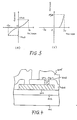
- Fig. 3(a) shows the electrical characteristic of the device before it is programmed.
- Fig. 3(b) shows the electrical characteristic after the device has been programmed by applying an electric field to induce an avalanche breakdown and producing an electric current of 2 to 3 mA. Before the device is programmed, the electrical characteristic curve is substantially symmetrical with respect to the direction in which the voltage is applied.
- the structure of the amorphous silicon film is partially changed by Joule heat produced by electric current.
- the P-type impurity is activated.
- PN junction diodes are created between the amorphous silicon film and the N+ -type diffused layer that acts as the lower electrode.
- FIG. 4 there is shown another semiconductor device according to the invention.
- This device is similar to the device shown in Fig. 1 except that the N+ -type diffused layer 103 acting as the lower electrode and shown in Fig. 1 is replaced by an N+ -type polycrystalline silicon film 403 on an oxide film 402.
- the device shown in Fig. 4 comprises a P-type semiconductor substrate 401, the locally formed oxidized film 402, the N+ -type polycrystalline silicon film 403, an interlayer insulating film 404, an amorphous silicon film 405 containing a P-type impurity, and a film 406 forming metal interconnections.
- the film 406 consists of two layers, i.e., a barrier metal layer and an aluminum layer formed on it, in the same way as in the device already described in connection with Fig. 1.
- the use of the N+ -type polycrystalline silicon film on the oxide film increases the degree of freedom to which the pattern is laid out. Further, the N+ -type polycrystalline silicon acting as the lower electrode is surrounded by the insulating film consisting of the silicon oxide film. Therefore, the Joule heat generated on programming does not readily escape. Consequently, the device can be programmed with lower electric current.
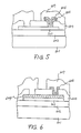
- a further semiconductor device comprises a P-type semiconductor substrate 501, an insulating film 502 consisting of a locally formed oxidized film, a low-resistance film 503, an interlayer insulating film 504, an N+ -type polycrystalline silicon film 505, an amorphous silicon film 506 containing a P-type impurity, and a film 507 forming metal interconnections.
- the low-resistance film 503 which acts as a lower electrode is made from a metal of a low resistance, such as Mo, Ti, or W, or a silicide of such a metal, such as MoSi2. Holes are formed in the interlayer insulating film 504.
- the substrate 501 is made from silicon. Silicon oxide is deposited on the substrate 501 to form the insulating film 502. Then, MoSi2 is sputtered on the insulating film 502 up to a thickness of 0.2 ⁇ m and photolithographically patterned to form the metal film 503 that serves as the lower electrodes of programmable elements. A silicon oxide film is deposited by a CVD process to form the interlayer insulating film 504. Holes extending through the insulating film 504 are formed at locations at which the N-type polycrystalline silicon film 505 and the amorphous silicon film 506 containing the P-type impurity are to be formed.
- the holes are formed in the insulating film 504 at locations at which direct connections with the metal film 503 forming the lower electrodes are made.
- N-type polycrystalline silicon is deposited up to a thickness of 0.2 ⁇ m.
- the polycrystalline silicon film 505 is etched into a desired pattern. Ions of phosphorus of 4 x 1015 cm ⁇ 2 are injected into the polycrystalline silicon at 60 keV by ion implantation, and then the laminate is annealed in an electric furnace to activate the impurities, thus forming the N-type polycrystalline silicon film 505.
- SiH4 is decomposed at a low temperature of 560°C by a CVD process to deposit amorphous silicon as a layer up to a thickness of 0.15 ⁇ m.
- Ions of boron fluoride of 1 x 10¹¹ to 1 x 1015 cm ⁇ 2 are implanted at 80 keV to obtain desired diode characteristics.
- the amorphous silicon film 506 containing a P-type impurity is formed.
- the doped amorphous silicon film 506 is etched into a desired pattern covering the N-type polycrystalline silicon film 505.
- a barrier metal and aluminum are successively sputtered to form the film 507 for forming the metal interconnections.
- this film 507 is patterned by photolithographic techniques. As a result, a read-only memory is created which can be programmed by dielectric breakdown.
- FIG. 6 there is shown still another semiconductor device according to the invention.
- This device comprises a P-type semiconductor substrate 601, an insulating film 602 that is a locally formed oxidized film, a low-resistance film 603 made from a low-resistance metal or metal silicide, such as MoSi2, an N+ -type polycrystalline silicon film 604 formed on the low-resistance film 603, an interlayer insulating film 605, an amorphous silicon film 606 containing a P-type impurity, and a film 607 forming metal interconnections.
- the low-resistance film 603 acts as a lower electrode.
- This semiconductor device is manufactured in the manner described below.
- the insulating film 602 consisting of a film of silicon oxide is formed on the semiconductor substrate 601 made from silicon.
- MoSi2 is sputtered on the laminate up to a thickness of 0.2 ⁇ m to form the metal film 603 which creates the lower electrodes of programmable elements.
- polycrystalline silicon is deposited on the laminate to a thickness of 0.2 ⁇ m.
- ions of phosphorus of 4 x 1015 cm ⁇ 2 are implanted at 60 keV, followed by annealing of the laminate inside an electric furnace to form the N-type polycrystalline silicon film 604.
- the metal film 603 and the N-type polycrystalline silicon film 604 are etched into a desired pattern by a photoetching technique. Then, silicon oxide is deposited as a film by chemical vapor deposition to form the interlayer insulating film 605. Holes extending through the insulating film are formed at locations at which the amorphous silicon film 606 containing a P-type impurity are to be formed, namely at locations at which direct connection with the N-type polysilicon film 604 forming a part of the lower electrode is to be made. Then, SiH4 is decomposed at a low temperature of 560°C by a CVD process to form the amorphous silicon layer of 0.15 ⁇ m thick.
- Ions of boron fluoride of 1 x 10¹¹ to 1 x 1015 cm ⁇ 2 are implanted at 80 keV to derive desired diode characteristics.
- the amorphous silicon film 606 containing a P-type impurity is formed and etched into a desired pattern.
- a barrier metal and aluminum are successively sively sputtered as films to form the film 607 creating metal interconnections.
- the laminate is etched into a desired pattern. In this way, a read-only memory which can be programmed by dielectric breakdown is made.
- the P-type semiconductor film can be P-type polycrystalline silicon. Also, it can be polycrystalline silicon or crystalline silicon whose crystalline structure has been destroyed by ion implantation or another technique.
- the P-type semiconductor film can be replaced with an N-type semiconductor film where the lower electrode is a P+ -type diffused layer.
- the metal film forming the lower electrode is made from MoSi2. It is also possible to fabricate the metal film from TiSi2 or WSi2. Further, the metal film can be polycide.
- the semiconductor substrate can be either P-type silicon or N-type silicon.
- the lower electrodes are made from a metal such as Mo, Ti, or W, or silicide of such a metal. This lowers the resistance of the lower electrodes. Therefore, where programmed regions are arranged in series, they can be programmed with lower electric current.
- the semiconductor films having a P-type impurity between lattices are formed by chemical vapor deposition and ion implantation. These films can also be created by sputtering.
- the semiconductor films may be made from polycrystalline silicon into which ions of a P-type impurity are injected. Also, they may be polycrystalline silicon or crystalline silicon whose crystalline structure has been destroyed by ion implantation.
- the P-type semiconductor film has an impurity between lattices.
- the lower electrode is a P+ -type diffused layer
- the film may be a semiconductor film containing an N-type impurity between lattices. In the examples shown in Figs.
- the metal films forming the lower electrodes are made from MoSi2. These films may also made from TiSi2, WSi2, W, or Mo.
- the film 106, 406, 507, and 607 which create metal interconnections to form upper electrodes may be one or more layers of aluminum, or a high-melting point metal such as W, Ti, Mo, or silicide thereof.
- the present invention is not limited to the aforementioned four examples, but various changes and modifications may be made without departing from the spirit and scope of the invention.
- the inventive semiconductor device comprises: a first semiconductor layer being of a first conductivity type; a second semiconductor layer which is formed on the first semiconductor layer, and contains an impurity between lattices, the impurity being of a second conductivity type different from the first conductivity type; and an upper electrode layer.
- the resistance of the first semiconductor film that is located just under a programmed film and has the first conductivity type is low. Also, it is not modulated with voltage. Since the structure is simple, the area of the patterned regions is small.
- the device is fabricated by simple processes. By forming the lower electrode over the substrate, the generated Joule heat is effectively utilized and so the device can be programmed with lower electric current.
- the resistance of the lower electrode is lowered by forming the lower electrode from a high-melting point metal such as Mo, Ti, or W, or silicide of such a metal, such as MoSi2, TiSi2, or WSi2.
- a high-melting point metal such as Mo, Ti, or W
- silicide of such a metal such as MoSi2, TiSi2, or WSi2.
Abstract
Description
- The present invention relates to a semiconductor device whose resistance value is varied from a high resistance to a low resistance irreversible by applying an electric field and, more particularly, to a semiconductor device usable for electrically programmable read-only memories.
- A so-called anti-fuse device having amorphous silicon layers inserted between successive electrodes has been used as a semiconductor device whose resistance value is varied from a high value to a low value irreversibly by applying an electric field. Especially, where anti-fuse devices are used in an electrically programmable read-only memory, it has been common practice to add a diode to each individual storage element, for making the ROM circuit configuration simpler. Such a diode is created by forming a Schottky junction on a lightly doped N-type semiconductor layer, the junction layer including platinum.
- A known semiconductor device is shown in Fig. 2, where a diffused layer formed in a silicon substrate is used as one electrode of a storage element. The silicon substrate, indicated by 201, is of the P type. Created on the substrate 201 are an oxidized film 202 forming a field-insulating film, an N⁺ -type diffused
layer 203, aninterlayer insulting film 204, an N⁻ -type diffused layer 205, a platinum silicide layer 206, anamorphous silicon film 207, and afilm 208 for forming metal interconnections. Theinsulating film 204 is made from silicon oxide, for example. - In this device, the N⁻ -type diffused layer 205 is in contact with the N⁺-type diffused
layer 203. the platinum silicide layer 206, theamorphous silicon film 207, and thefilm 208 for forming metal interconnections are laminated on the diffused layer 205 which serves as lower electrodes. Thefilm 208 acts as upper electrodes. In the operation, an electric field is applied between the upper and lower electrodes to cause an avalanche breakdown in the amorphous silicon film. At this time, Joule heat is evolved to change parts of the amorphous silicon film, thus forming low-resistance regions. The rectifying function of the Schottky diode between the platinum silicide layer and the N⁻ -type diffused layer is combined with the low-resistance regions of the amorphous silicon film to provide the known, electrically programmalbe read-only memory. - Another known semiconductor device is disclosed in U.S. Pat. No. 4,442,507. this device has a polycrystalline silicon layer which is formed on a silicon substrate and acts as one electrode of each storage element. In particular, a polycrystalline silicon layer is heavily doped so as to exhibit N type. Another polycrystalline silicon layer formed on the heavily doped silicon layer is lightly doped and of the N type. A platinum silicide layer, an amorphous silicon film, and a film forming metal interconnections are deposited on the lightly doped polycrystalline silicon layer. The film forming the metal interconnections forms upper electrodes. Schottky diodes that are created between the platinum silicide layer and the lightly doped N-type polycrystalline silicon layer are employed.
- In this known device, the lightly doped N-type diffused layer is formed to create the Schottky junctions. This presents the following problems.
- (1) The resistance obtained after programming the device increases by an amount equal to the resistance of the lightly doped N-type diffused layer (examples 1 and 2).
- (2) Where programmable elements are formed in series on the same lower electrode, the resistance of the lower electrode further increases by an amount equal to the resistance of the lightly doped N-type diffused layer (example 1).
- (3) The resistance of the thin N-type diffused layer is easily modulated with voltage and so the resistance values of the programmed device easily vary during operation (example 1).
- (4) When the thin N-type diffused layer is formed to create the Schottky junctions, it is necessary to take account of allowance for alignment. This increases the area of patterning (example 1).
- Accordingly, it is an object of the invention to provice a semiconductor device which shows low and stable resistance values after having been programmed and has a small patterned region, and in which, when an electric field is applied, the resistance irreversibly varies from a high resistance to a low resistance and then the device exhibits rectification.
- The above object is achieved in accordance with the teaching of the invention by a semiconductor device as claimed.
- In this configuration, the first semiconductor layer is of the N type, for example. The second semiconductor layer formed on the N-type semiconductor layer is an amorphous semiconductor film, a polycrystalline semiconductor film, or a semiconductor film whose crystalline structure has been destroyed by ion implantation or an other technique, and each film is lightly doped with a P-type impurity. Before the device is programmed, a P-type impurity exists between lattices in the noncrystalline or polycrystalline semiconductor film. In this state, the film is electrically inactive and, therefore, it shows a high resistance irrespective of the direction of the applied electric field. Once a high electric field is applied to the film deposited on the N-type semiconductor layer as lower electrodes, an avalanche breakdown take place, producing excessive electric current. This gives rise to Joule heat, which changes partially the crystalline structure of the programmed film that is lightly doped and contains a P-type impurity. Also, the P-type impurity is activated. As a result, the deposited film which showed a high resistance acts as a diode that exhibits a low resistance in the forward direction.
- Ways of carrying out the invention are described below with reference to drawings which illustrate only specific embodiments and in which:
- Fig. 1 is a cross-sectional view of main portions of a semiconductor device according to the invention;
- Fig. 2 is a cross-sectional view of main portions of a known semiconductor device;
- Fig. 3(a) is a graph showing the electrical characteristic of a semiconductor device according to the invention, which has not yet been programmed;
- Fig. 3(b) is a graph similar to Fig. 3(a), but in which the device has been programmed;
- Fig. 4 is a cross-sectional view of main portions of another semiconductor device according to the invention;
- Fig. 5 is a cross-sectional view of main portions of a further semiconductor device according to the invention; and
- Fig. 6 is a cross-sectional view of main portions of still another semiconductor device according to the invention.
- Referring to Fig. 1, there is shown a semiconductor device embodying the concept of the invention. This device comprises a P-
type semiconductor substrate 101 consisting of silicon or another material, an oxidizedfilm 102 locally formed on the substrate and constituting a field-insulating film and consisting of silicon oxide, for example, an N⁺ -type diffusedlayer 103, an interlayerinsulating film 104 consisting of silicon oxide, for example, anamorphous silicon film 105 containing a P-type impurity, and afilm 106 forming metal interconnections. Thefilm 106 consists of one or more layers formed from Al, or a metal having a high melting point such as Mo, Ti, or W, or a silicide of such a high-melting point metal. Theamorphous silicon film 105 having the P-type impurity and the upper electrode consisting of thefilm 106 are formed over the N⁺ -type diffusedlayer 103 that forms the lower electrodes. By programming the programmable elements having a high resistance, they show rectification as described previously. - This semiconductor device is fabricated in the manner described below. First, the oxidized
film 102 is locally formed on the P-type semiconductor substrate 101. Then, ions of phosphorus of 4 x 10¹⁵ cm⁻² are injected into thesilicon substrate 101 at 60 keV by an ion implantation technique to form the N⁺ -type diffusedlayer 103 which becomes the lower electrodes of the programmable elements. Subsequently, a film of silicon oxide is deposited by a CVD process to form theinterlayer insulating film 104. Openings necessary for direct connection with the N⁺-type diffusedlayer 103 are made. Also, openings required to make connection via theamorphous silicon film 105 containing the P-type impurity and constituting the main portions of the programmable elements are formed. Thereafter, SiH₄ is decomposed by a CVD process at a low temperature of 560°C to deposit an amorphous silicon film up to a thickness of 0.15µm. Boron fluoride of 1 x 10¹¹ to 1 x 10¹⁵ cm⁻² is introduced into the amorphous silicon film at 60 keV by ion implantation to obtain desired diode characteristics. Thus, theamorphous silicon film 105 containing the P-type impurity is formed. Thisamorphous film 105 is photolithographically patterned. Then, a barrier metal and aluminum are sputtered to form a laminate, which is then photolithographically patterned to create thefilm 106 for forming conductive interconnections. The resistance of the thus formed device is irreversibly changed from a high value to a low value by the application of an electric field. The device shows rectification. The oxidizedfilm 102 is formed by localized oxidation of silicon (LOCOS). It is also possible to form grooves in a semiconductor substrate and to insert an isulator in the grooves. The aforementioned barrier metal can be a metal having a high melting point such as Mo, Ti, or W, or a silicide or nitride of such a metal. Usually, the barrier metal is located under aluminum. - The electrical characteristics of the semiconductor device are described next. As an example, ions of boron fluoride of 1 x 10¹⁵ cm⁻² are injected at 60 keV into the amorphous silicon film containing the P-type impurity. Openings required to make connection via the amorphous silicon film have a diameter of 1.2 µm. Fig. 3(a) shows the electrical characteristic of the device before it is programmed. Fig. 3(b) shows the electrical characteristic after the device has been programmed by applying an electric field to induce an avalanche breakdown and producing an electric current of 2 to 3 mA. Before the device is programmed, the electrical characteristic curve is substantially symmetrical with respect to the direction in which the voltage is applied. Electric current of only 10 nA flowed at 5 V, i.e. the resistance is high. Once a voltage is applied to program the device, if a positive voltage is applied to the upper electrode that is an aluminum film overlying the amorphous silicon film, a forward characteristic is exhibited. If a negative voltage is applied, a reverse characteristic is obtained. In the case of an undoped amorphous silicon film, after the device has been programmed, the characteristic curve is substantially symmetrical with respect to the direction in which the voltage is applied, and the resistance is low. These changes in the electrical characteristic are considered as being brought about by the mechanism described above. That is, the structure of the amorphous silicon film is partially changed by Joule heat produced by electric current. The P-type impurity is activated. PN junction diodes are created between the amorphous silicon film and the N⁺ -type diffused layer that acts as the lower electrode.
- Referring next to Fig. 4, there is shown another semiconductor device according to the invention. This device is similar to the device shown in Fig. 1 except that the N⁺ -type diffused
layer 103 acting as the lower electrode and shown in Fig. 1 is replaced by an N⁺ -typepolycrystalline silicon film 403 on anoxide film 402. The device shown in Fig. 4 comprises a P-type semiconductor substrate 401, the locally formedoxidized film 402, the N⁺ -typepolycrystalline silicon film 403, an interlayer insulating film 404, anamorphous silicon film 405 containing a P-type impurity, and afilm 406 forming metal interconnections. Thefilm 406 consists of two layers, i.e., a barrier metal layer and an aluminum layer formed on it, in the same way as in the device already described in connection with Fig. 1. The use of the N⁺ -type polycrystalline silicon film on the oxide film increases the degree of freedom to which the pattern is laid out. Further, the N⁺ -type polycrystalline silicon acting as the lower electrode is surrounded by the insulating film consisting of the silicon oxide film. Therefore, the Joule heat generated on programming does not readily escape. Consequently, the device can be programmed with lower electric current. - Referring to Fig. 5, there is shown a further semiconductor device according to the invention. This device comprises a P-
type semiconductor substrate 501, an insulatingfilm 502 consisting of a locally formed oxidized film, a low-resistance film 503, aninterlayer insulating film 504, an N⁺ -typepolycrystalline silicon film 505, anamorphous silicon film 506 containing a P-type impurity, and afilm 507 forming metal interconnections. The low-resistance film 503 which acts as a lower electrode is made from a metal of a low resistance, such as Mo, Ti, or W, or a silicide of such a metal, such as MoSi₂. Holes are formed in theinterlayer insulating film 504. - This device is fabricated in the manner described now. The
substrate 501 is made from silicon. Silicon oxide is deposited on thesubstrate 501 to form the insulatingfilm 502. Then, MoSi₂ is sputtered on the insulatingfilm 502 up to a thickness of 0.2 µm and photolithographically patterned to form themetal film 503 that serves as the lower electrodes of programmable elements. A silicon oxide film is deposited by a CVD process to form theinterlayer insulating film 504. Holes extending through the insulatingfilm 504 are formed at locations at which the N-typepolycrystalline silicon film 505 and theamorphous silicon film 506 containing the P-type impurity are to be formed. That is, the holes are formed in the insulatingfilm 504 at locations at which direct connections with themetal film 503 forming the lower electrodes are made. Subsequently, N-type polycrystalline silicon is deposited up to a thickness of 0.2 µm. Thepolycrystalline silicon film 505 is etched into a desired pattern. Ions of phosphorus of 4 x 10¹⁵ cm⁻² are injected into the polycrystalline silicon at 60 keV by ion implantation, and then the laminate is annealed in an electric furnace to activate the impurities, thus forming the N-typepolycrystalline silicon film 505. Then, SiH₄ is decomposed at a low temperature of 560°C by a CVD process to deposit amorphous silicon as a layer up to a thickness of 0.15 µm. Ions of boron fluoride of 1 x 10¹¹ to 1 x 10¹⁵ cm⁻² are implanted at 80 keV to obtain desired diode characteristics. Thus, theamorphous silicon film 506 containing a P-type impurity is formed. Then, the dopedamorphous silicon film 506 is etched into a desired pattern covering the N-typepolycrystalline silicon film 505. Subsequently, a barrier metal and aluminum are successively sputtered to form thefilm 507 for forming the metal interconnections. Finally, thisfilm 507 is patterned by photolithographic techniques. As a result, a read-only memory is created which can be programmed by dielectric breakdown. - Referring next to Fig. 6, there is shown still another semiconductor device according to the invention. This device comprises a P-
type semiconductor substrate 601, an insulatingfilm 602 that is a locally formed oxidized film, a low-resistance film 603 made from a low-resistance metal or metal silicide, such as MoSi₂, an N⁺ -type polycrystalline silicon film 604 formed on the low-resistance film 603, an interlayer insulating film 605, anamorphous silicon film 606 containing a P-type impurity, and afilm 607 forming metal interconnections. The low-resistance film 603 acts as a lower electrode. - This semiconductor device is manufactured in the manner described below. First, the insulating
film 602 consisting of a film of silicon oxide is formed on thesemiconductor substrate 601 made from silicon. Then, MoSi₂ is sputtered on the laminate up to a thickness of 0.2 µm to form themetal film 603 which creates the lower electrodes of programmable elements. Then, polycrystalline silicon is deposited on the laminate to a thickness of 0.2 µm. Subsequently, ions of phosphorus of 4 x 10¹⁵ cm⁻² are implanted at 60 keV, followed by annealing of the laminate inside an electric furnace to form the N-type polycrystalline silicon film 604. Themetal film 603 and the N-type polycrystalline silicon film 604 are etched into a desired pattern by a photoetching technique. Then, silicon oxide is deposited as a film by chemical vapor deposition to form the interlayer insulating film 605. Holes extending through the insulating film are formed at locations at which theamorphous silicon film 606 containing a P-type impurity are to be formed, namely at locations at which direct connection with the N-type polysilicon film 604 forming a part of the lower electrode is to be made. Then, SiH₄ is decomposed at a low temperature of 560°C by a CVD process to form the amorphous silicon layer of 0.15 µm thick. Ions of boron fluoride of 1 x 10¹¹ to 1 x 10¹⁵ cm⁻² are implanted at 80 keV to derive desired diode characteristics. Thus, theamorphous silicon film 606 containing a P-type impurity is formed and etched into a desired pattern. A barrier metal and aluminum are succes sively sputtered as films to form thefilm 607 creating metal interconnections. Finally, the laminate is etched into a desired pattern. In this way, a read-only memory which can be programmed by dielectric breakdown is made. - In the examples of Figs. 5 and 6, chemical vapor deposition (CVD) and ion implantation are employed to fabricate the P-type semiconductor film. Instead, sputtering can be used. During chemical vapor deposition or sputtering, a dopant may be added. The P-type semiconductor film can be P-type polycrystalline silicon. Also, it can be polycrystalline silicon or crystalline silicon whose crystalline structure has been destroyed by ion implantation or another technique. The P-type semiconductor film can be replaced with an N-type semiconductor film where the lower electrode is a P⁺ -type diffused layer. In the above examples, the metal film forming the lower electrode is made from MoSi₂. It is also possible to fabricate the metal film from TiSi₂ or WSi₂. Further, the metal film can be polycide. Furthermore, the semiconductor substrate can be either P-type silicon or N-type silicon.
- In the examples shown in Figs. 5 and 6, the lower electrodes are made from a metal such as Mo, Ti, or W, or silicide of such a metal. This lowers the resistance of the lower electrodes. Therefore, where programmed regions are arranged in series, they can be programmed with lower electric current.
- In the aforementioned four examples, the semiconductor films having a P-type impurity between lattices are formed by chemical vapor deposition and ion implantation. These films can also be created by sputtering. The semiconductor films may be made from polycrystalline silicon into which ions of a P-type impurity are injected. Also, they may be polycrystalline silicon or crystalline silicon whose crystalline structure has been destroyed by ion implantation. In the above examples, the P-type semiconductor film has an impurity between lattices. Where the lower electrode is a P⁺ -type diffused layer, the film may be a semiconductor film containing an N-type impurity between lattices. In the examples shown in Figs. 5 and 6, the metal films forming the lower electrodes are made from MoSi₂. These films may also made from TiSi₂, WSi₂, W, or Mo. In the above-described four examples, the
film - As described thus far, the inventive semiconductor device comprises: a first semiconductor layer being of a first conductivity type; a second semiconductor layer which is formed on the first semiconductor layer, and contains an impurity between lattices, the impurity being of a second conductivity type different from the first conductivity type; and an upper electrode layer. The resistance of the first semiconductor film that is located just under a programmed film and has the first conductivity type is low. Also, it is not modulated with voltage. Since the structure is simple, the area of the patterned regions is small. In addition, the device is fabricated by simple processes. By forming the lower electrode over the substrate, the generated Joule heat is effectively utilized and so the device can be programmed with lower electric current. The resistance of the lower electrode is lowered by forming the lower electrode from a high-melting point metal such as Mo, Ti, or W, or silicide of such a metal, such as MoSi₂, TiSi₂, or WSi₂. Hence, a read-only memory capable of operating at a high speed can be obtained.
Claims (8)
a first semiconductor layer (103; 403; 505; 604) having a first conductivity type;
a second semiconductor layer (105; 405; 506; 606) which is formed on the first semiconductor layer and contains an impurity between lattices, the impurity being of a second conductivity type different from the first conductivity type; and
an upper electrode layer (106; 406; 507; 607).
Applications Claiming Priority (8)
| Application Number | Priority Date | Filing Date | Title |
|---|---|---|---|
| JP258833/88 | 1988-10-14 | ||
| JP25883388 | 1988-10-14 | ||
| JP122525/89 | 1989-05-16 | ||
| JP122526/89 | 1989-05-16 | ||
| JP12252689 | 1989-05-16 | ||
| JP12252589 | 1989-05-16 | ||
| JP175167/89 | 1989-07-06 | ||
| JP1175167A JP2525672B2 (en) | 1988-10-14 | 1989-07-06 | Semiconductor device |
Publications (2)
| Publication Number | Publication Date |
|---|---|
| EP0365932A1 true EP0365932A1 (en) | 1990-05-02 |
| EP0365932B1 EP0365932B1 (en) | 1994-08-31 |
Family
ID=27470862
Family Applications (1)
| Application Number | Title | Priority Date | Filing Date |
|---|---|---|---|
| EP89118999A Expired - Lifetime EP0365932B1 (en) | 1988-10-14 | 1989-10-12 | Semiconductor device |
Country Status (3)
| Country | Link |
|---|---|
| US (1) | US5093711A (en) |
| EP (1) | EP0365932B1 (en) |
| DE (1) | DE68917848T2 (en) |
Cited By (1)
| Publication number | Priority date | Publication date | Assignee | Title |
|---|---|---|---|---|
| WO2001043201A1 (en) * | 1999-12-08 | 2001-06-14 | Koninklijke Philips Electronics N.V. | Semiconductor device with a diode, and method of manufacturing such a device |
Families Citing this family (30)
| Publication number | Priority date | Publication date | Assignee | Title |
|---|---|---|---|---|
| US5989943A (en) * | 1989-09-07 | 1999-11-23 | Quicklogic Corporation | Method for fabrication of programmable interconnect structure |
| US5502315A (en) * | 1989-09-07 | 1996-03-26 | Quicklogic Corporation | Electrically programmable interconnect structure having a PECVD amorphous silicon element |
| US5552627A (en) * | 1990-04-12 | 1996-09-03 | Actel Corporation | Electrically programmable antifuse incorporating dielectric and amorphous silicon interlayers |
| US5272101A (en) * | 1990-04-12 | 1993-12-21 | Actel Corporation | Electrically programmable antifuse and fabrication processes |
| US5404029A (en) * | 1990-04-12 | 1995-04-04 | Actel Corporation | Electrically programmable antifuse element |
| US5780323A (en) * | 1990-04-12 | 1998-07-14 | Actel Corporation | Fabrication method for metal-to-metal antifuses incorporating a tungsten via plug |
| US5614756A (en) * | 1990-04-12 | 1997-03-25 | Actel Corporation | Metal-to-metal antifuse with conductive |
| US5541441A (en) * | 1994-10-06 | 1996-07-30 | Actel Corporation | Metal to metal antifuse |
| EP0480580A3 (en) * | 1990-09-10 | 1992-09-02 | Canon Kabushiki Kaisha | Electrode structure of semiconductor device and method for manufacturing the same |
| US5322812A (en) * | 1991-03-20 | 1994-06-21 | Crosspoint Solutions, Inc. | Improved method of fabricating antifuses in an integrated circuit device and resulting structure |
| US5701027A (en) * | 1991-04-26 | 1997-12-23 | Quicklogic Corporation | Programmable interconnect structures and programmable integrated circuits |
| US5110754A (en) * | 1991-10-04 | 1992-05-05 | Micron Technology, Inc. | Method of making a DRAM capacitor for use as an programmable antifuse for redundancy repair/options on a DRAM |
| JP2808965B2 (en) * | 1992-02-19 | 1998-10-08 | 日本電気株式会社 | Semiconductor device |
| EP0558176A1 (en) * | 1992-02-26 | 1993-09-01 | Actel Corporation | Metal-to-metal antifuse with improved diffusion barrier layer |
| US5284788A (en) * | 1992-09-25 | 1994-02-08 | Texas Instruments Incorporated | Method and device for controlling current in a circuit |
| US5308795A (en) * | 1992-11-04 | 1994-05-03 | Actel Corporation | Above via metal-to-metal antifuse |
| US5369054A (en) * | 1993-07-07 | 1994-11-29 | Actel Corporation | Circuits for ESD protection of metal-to-metal antifuses during processing |
| US5581111A (en) * | 1993-07-07 | 1996-12-03 | Actel Corporation | Dielectric-polysilicon-dielectric antifuse for field programmable logic applications |
| US5856234A (en) * | 1993-09-14 | 1999-01-05 | Actel Corporation | Method of fabricating an antifuse |
| US5592016A (en) * | 1995-04-14 | 1997-01-07 | Actel Corporation | Antifuse with improved antifuse material |
| US5789764A (en) * | 1995-04-14 | 1998-08-04 | Actel Corporation | Antifuse with improved antifuse material |
| JP3027195B2 (en) * | 1995-06-02 | 2000-03-27 | アクテル・コーポレイション | Raised tungsten plug antifuse and method of manufacturing the same |
| US5741720A (en) * | 1995-10-04 | 1998-04-21 | Actel Corporation | Method of programming an improved metal-to-metal via-type antifuse |
| US5909049A (en) | 1997-02-11 | 1999-06-01 | Actel Corporation | Antifuse programmed PROM cell |
| JP3488681B2 (en) * | 1999-10-26 | 2004-01-19 | シャープ株式会社 | Liquid crystal display |
| US6344669B1 (en) * | 2000-06-13 | 2002-02-05 | United Microelectronics Corp. | CMOS sensor |
| US6633182B2 (en) | 2001-09-05 | 2003-10-14 | Carnegie Mellon University | Programmable gate array based on configurable metal interconnect vias |
| US7132350B2 (en) | 2003-07-21 | 2006-11-07 | Macronix International Co., Ltd. | Method for manufacturing a programmable eraseless memory |
| US7180123B2 (en) * | 2003-07-21 | 2007-02-20 | Macronix International Co., Ltd. | Method for programming programmable eraseless memory |
| US20050035429A1 (en) * | 2003-08-15 | 2005-02-17 | Yeh Chih Chieh | Programmable eraseless memory |
Citations (3)
| Publication number | Priority date | Publication date | Assignee | Title |
|---|---|---|---|---|
| US4174521A (en) * | 1978-04-06 | 1979-11-13 | Harris Corporation | PROM electrically written by solid phase epitaxy |
| EP0065916A2 (en) * | 1981-05-15 | 1982-12-01 | Fairchild Semiconductor Corporation | Schottky diode - polycrystalline silicon resistor memory cell |
| US4590589A (en) * | 1982-12-21 | 1986-05-20 | Zoran Corporation | Electrically programmable read only memory |
Family Cites Families (9)
| Publication number | Priority date | Publication date | Assignee | Title |
|---|---|---|---|---|
| GB1399163A (en) * | 1972-11-08 | 1975-06-25 | Ferranti Ltd | Methods of manufacturing semiconductor devices |
| CA1136773A (en) * | 1978-08-14 | 1982-11-30 | Norikazu Ohuchi | Semiconductor device |
| US4442507A (en) * | 1981-02-23 | 1984-04-10 | Burroughs Corporation | Electrically programmable read-only memory stacked above a semiconductor substrate |
| US4424579A (en) * | 1981-02-23 | 1984-01-03 | Burroughs Corporation | Mask programmable read-only memory stacked above a semiconductor substrate |
| US4431460A (en) * | 1982-03-08 | 1984-02-14 | International Business Machines Corporation | Method of producing shallow, narrow base bipolar transistor structures via dual implantations of selected polycrystalline layer |
| US4583106A (en) * | 1983-08-04 | 1986-04-15 | International Business Machines Corporation | Fabrication methods for high performance lateral bipolar transistors |
| US4598386A (en) * | 1984-04-18 | 1986-07-01 | Roesner Bruce B | Reduced-area, read-only memory |
| JPS62104066A (en) * | 1985-10-31 | 1987-05-14 | Toshiba Corp | Semiconductor protecting device |
| US4823181A (en) * | 1986-05-09 | 1989-04-18 | Actel Corporation | Programmable low impedance anti-fuse element |
-
1989
- 1989-10-11 US US07/419,657 patent/US5093711A/en not_active Expired - Lifetime
- 1989-10-12 EP EP89118999A patent/EP0365932B1/en not_active Expired - Lifetime
- 1989-10-12 DE DE68917848T patent/DE68917848T2/en not_active Expired - Fee Related
Patent Citations (3)
| Publication number | Priority date | Publication date | Assignee | Title |
|---|---|---|---|---|
| US4174521A (en) * | 1978-04-06 | 1979-11-13 | Harris Corporation | PROM electrically written by solid phase epitaxy |
| EP0065916A2 (en) * | 1981-05-15 | 1982-12-01 | Fairchild Semiconductor Corporation | Schottky diode - polycrystalline silicon resistor memory cell |
| US4590589A (en) * | 1982-12-21 | 1986-05-20 | Zoran Corporation | Electrically programmable read only memory |
Non-Patent Citations (1)
| Title |
|---|
| INTERNATIONAL ELECTRON DEVICES MEETING, 6th-9th December 1987, Washington D.C., pages 194-197, IEEE, New York, US; Y. SHACHAM-DIAMAND et al.: "A novel ion-implanted amorphous silicon programmable element" * |
Cited By (1)
| Publication number | Priority date | Publication date | Assignee | Title |
|---|---|---|---|---|
| WO2001043201A1 (en) * | 1999-12-08 | 2001-06-14 | Koninklijke Philips Electronics N.V. | Semiconductor device with a diode, and method of manufacturing such a device |
Also Published As
| Publication number | Publication date |
|---|---|
| EP0365932B1 (en) | 1994-08-31 |
| DE68917848D1 (en) | 1994-10-06 |
| DE68917848T2 (en) | 1995-02-02 |
| US5093711A (en) | 1992-03-03 |
Similar Documents
| Publication | Publication Date | Title |
|---|---|---|
| EP0365932A1 (en) | Semiconductor device | |
| EP0118158B1 (en) | Programmable read-only memory structure and method of fabricating such structure | |
| US4748490A (en) | Deep polysilicon emitter antifuse memory cell | |
| US4943538A (en) | Programmable low impedance anti-fuse element | |
| CA1181848A (en) | Programmable cell for use in programmable electronic arrays | |
| EP0250078B1 (en) | Programmable low impedance interconnect circuit element | |
| US5070383A (en) | Programmable memory matrix employing voltage-variable resistors | |
| US4569121A (en) | Method of fabricating a programmable read-only memory cell incorporating an antifuse utilizing deposition of amorphous semiconductor layer | |
| US5144404A (en) | Polysilicon Schottky clamped transistor and vertical fuse devices | |
| EP0095411B1 (en) | Bipolar memory cell | |
| US5250459A (en) | Electrically programmable low resistive antifuse element | |
| US5210598A (en) | Semiconductor element having a resistance state transition region of two-layer structure | |
| US7332791B2 (en) | Electrically programmable polysilicon fuse with multiple level resistance and programming | |
| SE451514B (en) | PROGRAMMABLE CELL CONSISTING OF AN AMORPH CELL BODY, AND NETWORK OF SUCH CELLS | |
| KR100196484B1 (en) | Method to fabricate vertical fuse devices and schottky diodes using thin sacrificial layer | |
| JPS60226163A (en) | Method of producing cmos structure having schottky bipolar transistor | |
| US4375717A (en) | Process for producing a field-effect transistor | |
| US5436496A (en) | Vertical fuse device | |
| EP0080730B1 (en) | Semiconductor device with wiring layers and method of manufacturing the same | |
| EP0172193B1 (en) | Programmable read-only memory cell and method of fabrication | |
| US4692787A (en) | Programmable read-only-memory element with polycrystalline silicon layer | |
| US5212102A (en) | Method of making polysilicon Schottky clamped transistor and vertical fuse devices | |
| KR940008564B1 (en) | Semiconductor device and manufacturing method thereof | |
| EP0078220B1 (en) | Polycrystalline silicon interconnections for bipolar transistor flip-flop | |
| KR950001758B1 (en) | Semiconductor device |
Legal Events
| Date | Code | Title | Description |
|---|---|---|---|
| PUAI | Public reference made under article 153(3) epc to a published international application that has entered the european phase |
Free format text: ORIGINAL CODE: 0009012 |
|
| AK | Designated contracting states |
Kind code of ref document: A1 Designated state(s): DE FR NL |
|
| 17P | Request for examination filed |
Effective date: 19901010 |
|
| 17Q | First examination report despatched |
Effective date: 19930208 |
|
| GRAA | (expected) grant |
Free format text: ORIGINAL CODE: 0009210 |
|
| AK | Designated contracting states |
Kind code of ref document: B1 Designated state(s): DE FR NL |
|
| REF | Corresponds to: |
Ref document number: 68917848 Country of ref document: DE Date of ref document: 19941006 |
|
| ET | Fr: translation filed | ||
| PLBE | No opposition filed within time limit |
Free format text: ORIGINAL CODE: 0009261 |
|
| STAA | Information on the status of an ep patent application or granted ep patent |
Free format text: STATUS: NO OPPOSITION FILED WITHIN TIME LIMIT |
|
| 26N | No opposition filed | ||
| PGFP | Annual fee paid to national office [announced via postgrant information from national office to epo] |
Ref country code: DE Payment date: 20061005 Year of fee payment: 18 |
|
| PGFP | Annual fee paid to national office [announced via postgrant information from national office to epo] |
Ref country code: NL Payment date: 20061015 Year of fee payment: 18 |
|
| NLV4 | Nl: lapsed or anulled due to non-payment of the annual fee |
Effective date: 20080501 |
|
| PG25 | Lapsed in a contracting state [announced via postgrant information from national office to epo] |
Ref country code: DE Free format text: LAPSE BECAUSE OF NON-PAYMENT OF DUE FEES Effective date: 20080501 |
|
| REG | Reference to a national code |
Ref country code: FR Ref legal event code: ST Effective date: 20080630 |
|
| PG25 | Lapsed in a contracting state [announced via postgrant information from national office to epo] |
Ref country code: NL Free format text: LAPSE BECAUSE OF NON-PAYMENT OF DUE FEES Effective date: 20080501 |
|
| PGFP | Annual fee paid to national office [announced via postgrant information from national office to epo] |
Ref country code: FR Payment date: 20061010 Year of fee payment: 18 |
|
| PG25 | Lapsed in a contracting state [announced via postgrant information from national office to epo] |
Ref country code: FR Free format text: LAPSE BECAUSE OF NON-PAYMENT OF DUE FEES Effective date: 20071031 |