EP0364261A2 - Highly efficient coding apparatus - Google Patents
Highly efficient coding apparatus Download PDFInfo
- Publication number
- EP0364261A2 EP0364261A2 EP89310440A EP89310440A EP0364261A2 EP 0364261 A2 EP0364261 A2 EP 0364261A2 EP 89310440 A EP89310440 A EP 89310440A EP 89310440 A EP89310440 A EP 89310440A EP 0364261 A2 EP0364261 A2 EP 0364261A2
- Authority
- EP
- European Patent Office
- Prior art keywords
- data
- picture element
- block
- digital video
- video data
- Prior art date
- Legal status (The legal status is an assumption and is not a legal conclusion. Google has not performed a legal analysis and makes no representation as to the accuracy of the status listed.)
- Granted
Links
Images


Classifications
-
- H—ELECTRICITY
- H04—ELECTRIC COMMUNICATION TECHNIQUE
- H04N—PICTORIAL COMMUNICATION, e.g. TELEVISION
- H04N19/00—Methods or arrangements for coding, decoding, compressing or decompressing digital video signals
- H04N19/65—Methods or arrangements for coding, decoding, compressing or decompressing digital video signals using error resilience
- H04N19/68—Methods or arrangements for coding, decoding, compressing or decompressing digital video signals using error resilience involving the insertion of resynchronisation markers into the bitstream
-
- H—ELECTRICITY
- H04—ELECTRIC COMMUNICATION TECHNIQUE
- H04N—PICTORIAL COMMUNICATION, e.g. TELEVISION
- H04N19/00—Methods or arrangements for coding, decoding, compressing or decompressing digital video signals
- H04N19/50—Methods or arrangements for coding, decoding, compressing or decompressing digital video signals using predictive coding
- H04N19/587—Methods or arrangements for coding, decoding, compressing or decompressing digital video signals using predictive coding involving temporal sub-sampling or interpolation, e.g. decimation or subsequent interpolation of pictures in a video sequence
-
- H—ELECTRICITY
- H04—ELECTRIC COMMUNICATION TECHNIQUE
- H04N—PICTORIAL COMMUNICATION, e.g. TELEVISION
- H04N19/00—Methods or arrangements for coding, decoding, compressing or decompressing digital video signals
- H04N19/90—Methods or arrangements for coding, decoding, compressing or decompressing digital video signals using coding techniques not provided for in groups H04N19/10-H04N19/85, e.g. fractals
- H04N19/98—Adaptive-dynamic-range coding [ADRC]
Definitions
- This invention relates to a highly efficient coding apparatus for a picture signal such as a television signal and, more particularly, to a structure in which subsampling and a block coding such as a coding adaptive to the dynamic range of the picture signal, and the like are combined.
- JP,A Japanese patent laid open publication
- a picture is divided into a number of two-dimensional blocks, the difference (dynamic range) between the maximum value and the minimum value of the data of a number of picture elements in the block is obtained, and the period of the subsampling is varied depending on the dynamic range of the blocks. More specifically, with respect to a block having a small dynamic range, it is judged to be a planar picture, and the subsampling period is lengthened to (1/8), for example.
- the subsampling period is set for a unit of a block in a highly efficient coding apparatus switching a subsampling frequency selectively depending on dynamic range as described above, whether the picture quality of a reproduced picture is good or poor occurs is determined for a unit of a block. For this reason, noticeable block distortion may appear. Also, the subsampling periods available for selection are limited, so that the adaptability to the characteristics of a particular picture is inadequate.
- the present applicant has proposed a highly efficient coding apparatus for a picture signal which does not cause the deterioration on a per-block basis and which can form a subsampling pattern having variable density adaptive to a characteristic of a picture so as to provide an excellent reproduction picture (refer to the specification of the Japanese patent application number 208975/1987).
- variable density subsampling since the thinning-out process is done adaptively, the amount of generated data varies greatly depending on the degree of correlation of a picture. As a consequence, there are problems in ensuring that the amount of data transmitted does not exceed a predetermined value and where the technique is applied to a transmission path (for example, a digital VTR) which requires an almost constant data rate. Also, in the case of a small transmission capacity, a sufficient reduction in the amount of data amount is not achieved only by the subsampling.
- a highly efficient coding apparatus for coding digital video data in a format composed of blocks of digital video data representing plural picture elements and allowing compression of the video data, comprising: means for receiving the digital video data represented by respective picture element data having a first predetermined number of bits per element, means for designating at least one picture element for each of said blocks as an elementary picture element, means for predicting values of respective ones of subject picture element data, means for detecting respective predictive errors of the predicted values from the real values of the picture element data, means for determining if each predictive error is greater than a threshold value, means for generating flag data by the output of said determining means, means for gating said elementary picture element data and the subject picture element data for which the respective predictive errors are greater than the threshold value, first and second detecting means for detecting maximum and minimum values, respectively of the output of said gating means in each of said blocks, means for generating dynamic range information for each said block from said maximum and minimum values for the respective block, means for generating modified digital video data for each
- the present invention can provide an improved highly efficient coding apparatus which can attain high compression ratio by employing compression in the level direction, which minimises the quality deterioration of the reproduced image, while allowing the amount of the transmitted data in a block to be substantially fixed, and which requiring only small capacity buffer memory.
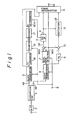
- Figure 1 shows a first embodiment of this invention, and in figure 1, a picture signal, for instance, a video signal is supplied to an input terminal indicated by 1.
- the video signal is converted into a digital video signal by an A/D converter 2.
- the digital video signal has a sampling frequency of 13.5 [MHz] as an example, and one picture element data is converted to a data word of eight bits.
- the digital video signal is supplied to a subsampling encoder 3.
- data of a picture element to be transmitted is generated at an output terminal 48 of the subsampling encoder 3 after a thinning-out process, and a control code is generated at an output terminal 49. Transmission or thinning-out of respective picture element is identified by the control code.
- An ADRC encoder is provided on the output side of the subsampling encoder 3, and encoding is made to be adaptive to the dynamic range DR of data of a two-dimensional block of data, for example.
- the digitisation bit number N in the ADRC encoder is set depending on the subsampling rate in the subsampling encoder 3. The subsampling rate is judged every block. In this embodiment, the digitisation bit number is set at any one of the possible bit numbers (8, 7, 6, 5, 4, 3, 2, 1).
- a digital video signal is given to an input terminal indicated by 21 from the A/D converter 2.
- a series circuit of line delay circuits 22, 23, 24, 25 indicated by LD is connected to the input terminal 21.
- sample delay circuits 26 and 27 indicated by SD are connected in series with respect to the input terminal 21
- sample delay circuits 28 and 29 are serially coupled on the output side of the line delay circuit 22
- sample delay circuits 30, 31, 32 and 33 are connected in series on the output side of the line delay circuit
- sample delay circuits 34 and 35 are serially coupled on the output side of the line delay circuit 24
- sample delay circuits 36 and 37 are coupled in series on the output side of the line delay circuit 25.
- line delay circuits 22, 23, 24, 25 have a delay amount of one horizontal period, respectively, and the sample delay circuits 26, 27, 28, ..., 37 have a delay amount of one sampling period, respectively.
- Data of plural picture elements contained in a predetermined two-dimensional area of a television picture are simultaneously taken out by the line delay circuits 22 to 25 and the sample delay circuits 26 to 37.
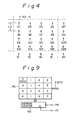
- Figure 4 shows a part of the area of the two-dimensional (field or frame) of an input digital video signal.
- an interval of picture elements in the horizontal direction corresponds to a sampling period SD
- an interval of picture elements in the vertical direction corresponds to a line interval LD.
- Each of symbols ( ⁇ , ⁇ , ⁇ , ⁇ , ⁇ ) attached to each picture element the differing interpolation procedures applied to them.
- ⁇ represents an elementary picture element occurring every four lines and every four picture elements.
- One elementary picture element out of the 16 picture elements is necessarily transmitted without being subjected to thinning-out.
- Picture elements other than the elementary picture element are compared with an average value of two picture elements as mentioned below, and when a difference (predictive error) between picture element data and the average value is equal to or smaller than a threshold value, the thinning-out is carried out. Conversely, when the predictive error exceeds the threshold value, the transmission is carried out without thinning-out.
- the output data of the sample delay circuit 31 is a subject picture element.
- the output data of the sample delay circuit 31 is supplied to fifth input terminals of the selectors 38 and 39, the subtractor 43 and the gate circuit 47.
- the selectors 38 and 39 have first to fifth input terminals.
- the selectors 38 and 39 sequentially and selectively produce input data respectively applied to these five input terminals to their output terminals by a selecting signal from a terminal 40 which is synchronised with a sampling clock.
- the output data of the sample delay circuit 27 is supplied to the first input terminal of the selector 38, and the output data of the sample delay circuit 37 is applied to the first input terminal of the selector 39.
- a subject picture element is a picture element indicated by ⁇
- input data respectively supplied to the first input terminals of the selectors 38 and 39 are selected.
- the output data of the sample delay circuits 29 and 35 are supplied to the second input terminals of the selectors 38 and 39, respectively. Consequently, in the case where a subject picture element is a picture element represented by ⁇ , input data supplied to the respective second input terminals of the selectors 38 and 39 are selected.
- the output data of the line delay circuit 23 and the output data of the sample delay circuit 33 are supplied to the third input terminals of the selectors 38 and 39, respectively.
- input data supplied to the respective third input terminals of the selectors 38 and 39 are selected.
- the output data of the sample delay circuits 30 and 32 are given to fourth input terminals of the selectors 38 and 39. Therefore, when a subject picture element is the one represented by ⁇ , input data supplied to the fourth input terminals of the selectors 38 and 39 are selected.
- the output data (subject picture element) of the sample delay circuit 31 is applied to the fifth input terminals of the selectors 38 and 39. Consequently, when a subject picture element is the elementary picture element represented by ⁇ , both of the selectors 38 and 39 select the elementary picture element.
- the output data of the selectors 38 and 39 are fed to an adder 41, and the output signal of the adder 41 is fed to a 1/2 multiplication circuit 42.
- the average value data of two picture elements respectively selected by the selectors 38 and 39 is generated from the 1/2 multiplication circuit 42.
- the average value data and data of the subject picture element from the sample delay circuit 31 are supplied to a subtractor 43, and difference data from the subtractor 43 is converted into absolute values at an absolute-value-generating circuit 44.
- the output data of the absolute-value-generating circuit 44 is supplied to a comparator 45 and compared with a threshold value from a terminal 46.
- the output data of the absolute-value-generating circuit 44 represents a predictive error generated when an interpolation is performed by the average value of two picture elements.
- a control code (1 bit) from the comparator 45 is brought to "1", since it means that the picture element can be thinned out.
- the control code from the comparator 45 is brought to "0", because it means that the interpolation cannot be performed well on the reception side.
- the ON/OFF of a gate circuit 47 is controlled by this control code.
- control code When the control code is "0", the gate circuit 47 is turned on so that original picture element data is output at an output terminal 48, whereas when the control code is "1", the gate circuit 47 is turned off so as not to output the original picture element data at the output terminal 48.
- control code is produced at an output terminal 49 and provided together with subsampled video data as an output.
- the predictive error of each elementary picture element ⁇ becomes zero, which is equal to or less than a threshold value.
- this elementary picture element is exceptionally treated. It is needless to say that the gate circuit 47 should be controlled so that the elementary picture element date might be taken out at the output terminal 48 through the gate circuit 47.
- the subsampling is done depending on whether or not the predictive error is below a threshold value. More specifically, the transmission/thinning-out is adaptively controlled on a picture-element by picture-element basis rather than a block of picture elements treated as a whole. Also, when the decision is made on whether the thinning-out should be done by obtaining the predictive error, real data is always employed without using interpolation data. For this reason, repeated processing can be avoided, so enabling real-time processing. Needless to say, in the case of a small predictive error, the value of a picture element to be thinned out by be replaced by interpolation data, and this interpolation data may be employed at the time of the decision as to the next predictive error.
- the picture element data and the control code taken out at the output terminals 48 and 49 are supplied to the block segmentation circuits 5 and 6, respectively.
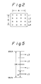
- the block segmentation circuits 4 and 5 convert the sequence of the picture element date and the control code so as to arrange them in block order as shown in figure 2.
- a clock signal with a block period is supplied to these block segmentation circuits 4 and 5 from a terminal 6.
- broken lines show boundaries corresponding to blocks.
- the range of the thinning-out rates may extend from (1/16) which allows the transmission of only elementary picture element data per block to (16/16) which allows the transmission of data of all picture elements in a block.
- the output data of the block segmentation circuit 4 is supplied to a maximum value and minimum value detector 7 and to a subtractor 10 through a delay circuit 8. Clocks from the terminal 6 are supplied to the maximum value and minimum value detector 7, and a maximum value MAX and a minimum value MIN are detected for each block.
- the maximum value MAX and the minimum value MIN are supplied to a subtractor 9, so that the dynamic range DR represented by (MAX-MIN) is provided from the subtractor 9.
- the minimum value MIN is supplied to the subtractor 10, and picture element date from which the minimum value has been eliminated is produced from the subtractor 10.
- This picture element data is fed to a digitisation circuit 12.
- a digitisation step ⁇ is supplied to the digitisation circuit 12 from a digitisation step generator 11, data which is normalised by the elimination of the minimum value is divided by the digitisation step ⁇ , and the result of the division is subjected to truncation to eliminate any fractional part of the result, thereby to form a coded data DT.
- the digitisation step generator 11 and the digitisation circuit 12 need not be composed not only of a division circuit but instead could be a look-up table, eg stored in ROM.
- Figure 5 shows the digitisation operation in the case of a digitisation bit number of 2 bits.
- the digitisation step ⁇ is formed. Data from which the minimum value has been eliminated is divided by the digitisation step ⁇ , any fractional result is discarded, so providing a two-bit coded data DT.
- L0 to L3 indicate decoded levels (representative values) corresponding to coded data (00), (01) (10) (11), respectively.
- a bit number N is supplied to the digitisation step generator 11 from a bit-number-determining circuit 18. This bit number N is determined corresponding to the thinning-out rate in the subsampling encoder 3.
- a control code is converted into the order of blocks by the block segmentation circuit 5. The control code from the block segmentation circuit 5 is fed to a "1" separation circuit 15. As described before, a "1" in the control code indicates a thinning-out picture element subject to thinning out.
- the separated "1" control code is supplied to a counter 16.
- the counter 16 is reset by a clock signal from the terminal 6, and, consequently, the number of picture elements to be thinned-out is counted by the counter 16.
- the count value of the counter 16 is decoded at a decoder 17, and the output of the decoder 17 is supplied to the bit-number-determining circuit 18.
- the decoder 17 is not always needed.
- the bit-number-determining circuit 18 is composed of a ROM and determines a digitisation bit number on the basis of the number of picture elements to be thinned out
- N 8.
- N 6.
- N 5.
- N 4.
- N 3.
- N 1.
- the digitisation circuit 12 performs a digitisation by the bit number N determined by this bit-number-determining circuit 18.
- the control code from the block segmentation circuit 5, the digitisation step ⁇ from the digitisation step generator 11, the minimum value MIN and the coded data DT are supplied to a frame segmentation circuit 13 and converted into transmission data of a frame structure. Encoding of error correction is done at the frame segmentation circuit 13 when necessary. Transmission data is output from an output terminal 14 of the frame segmentation circuit 13.
- the compression rate can be increased. Because this embodiment varies the digitisation bit number of the ADRC depending on the degree of the thinning-out of the subsampling, the control can be such that the generated data amount does not exceed the transmission capacity or such that the generated data amount is almost constant.
- a digital picture signal for instance, a digital video signal is supplied to an input terminal indicated by 101.
- the digital video signal has a sampling frequency of 13.5 [MHz] as an example, and one picture element data is made represented by an eight bit word.
- the digital video signal is supplied to a block segmentation circuit 102.
- the block segmentation circuit 102 divides the picture of one field (or one frame) into a plurality of blocks B11, B12, ..., BNM as shown in figure 7. For instance, each block has a structure of (4 x 4 elements) as described above with reference to figure 2, so one block, contains the data of 16 picture elements.
- the sequence of data generated from the block segmentation circuit 102 is indicated by an arrow showing the block order in figure 7.
- 16 picture elements are transmitted sequentially from a picture element on the left-hand side in a line L1 of figure 2 to those in lines L2, L3, L4.
- the output data of the block segmentation circuit 102 is supplied to a maximum value detector 103 and a minimum value detector 104 and to a subtractor 106 through a delay circuit 105.
- the maximum value MAX and the minimum value MIN are detected for each block by the maximum value detector 103 and the minimum value detector 104.
- the maximum value MAX and the minimum value MIN are supplied to a subtractor 107, so that a dynamic range DR represented by (MAX-MIN) is provided from the subtractor 107.
- the minimum value MIN is supplied to the subtractor 106, and picture element data from which the minimum value has been eliminated is produced from the subtractor 106.
- This picture element data is fed to a digitisation circuit 108.
- a digitisation step ⁇ is supplied to the digitisation circuit 108 from a digitisation step generator 110, data which is normalised by the elimination of the minimum value is divided by the digitisation step ⁇ , and any fractional result of the division is discarded, thereby to form a coded data DT.
- the coded data DT has a fixed bit number of 2 bits, for example.
- the digitisation step generator 110 and the digitisation circuit 108 need not be a division circuit but could instead be a look-up table stored in ROM.
- the dynamic range DR is divided into four level ranges by a digitisation step ⁇ and the two-bit coded data DT is allocated depending on a value of data from which the minimum value is eliminated.
- a decoded level lies in the centre of the width of the digitisation step, for example.
- the dynamic range DR and the minimum value MIN are supplied to a frame segmentation circuit 115 through delay circuits 111 and 112.
- the coded data DT from the digitisation circuit 108 is given to a gate circuit 114 for subsampling through a delay circuit 113.
- the delay time DL3 of the delay circuit 113 is set at (4LD + 4SD).
- a gate signal formed as mentioned later is fed to the gate circuit 114, and the coded data DT is selectively generated from the gate circuit 114.
- the output signal of the gate circuit 114 is supplied to the frame segmentation circuit 115.
- the gate signal is a bit map for indicating whether a given element is to be transmitted as is, or subject to thinning-out, and the bit map is supplied to the frame segmentation circuit 115, as well.
- the frame segmentation circuit 115 encoding of error correction is done as needed.
- the transmission data is taken out at an output terminal 116 of the frame segmentation circuit 115.
- the transmission of arbitrary two data items selected from the dynamic range DR, the minimum value MIN, and the maximum value MAX is needed.
- Gate signals for controlling the transmission of the coded data generated at the ADRC and the thinning-out are produced depending on the magnitude of the interpolation error.
- the same interpolation manner as the manner for interpolating data of thinned out picture elements on the reception side is applied to the detection of the interpolation error.
- a digital video signal converted into the sequence of blocks is supplied to an interpolation error detector 117 from the block segmentation circuit 102.
- the interpolation error detected at the interpolation error detector 117 is supplied to a memory 118, and the interpolation errors corresponding to each of 16 picture elements of one block is written into the memory 118. In this case, since one elementary picture element is necessarily sent for every block, the detection and storage of interpolation errors with respect to other picture elements may be carried out.
- the interpolation error read out of the memory 118 is supplied to a gate signal generator 119.
- the gate signal generator 119 specifies 8 picture elements in increasing order of interpolation error size among the supplied 16 interpolation errors.
- the gate signal generator 119 generates a gate signal to transmit the coded data DT of these 8 picture elements through the gate circuit 114.
- the predictive error of each elementary picture element becomes zero, which is the smallest predictive error.
- this elementary picture element is exceptionally treated. It is needless to say that the gate signal generator 119 should be controlled so that the elementary picture element data may pass through the gate circuit 114 when required.
- Delay circuits 131, 132, 133, 134, 135, 136, 137, 138, 139, 140, 141, 142 are connected in a serial chain to an input terminal 130 supplied with the digital video signal from the block segmentation circuit 102.
- the delay circuits 131 and 133 are line delay circuits and have a delay time of one line, as indicated by LD.
- the delay circuit 132 has a delay time of 2LD.
- the delay circuits 134 to 141 have a delay time of a sampling period, as indicated by SD.
- the delay circuit 142 has a delay amount of 4SD.
- the arrangement of picture elements of one block is the same as shown in figure 4.
- the interpolation method used differs for individual picture elements, as mentioned above.
- the digital video signal is a signal before block segmentation.
- the time interval between each picture element is different from that in the foregoing description. Namely, in figure 4, the time interval between S1 and S5 is shown to be delay time LD of one line, while in this embodiment the time interval between S1 and S5 is 4SD, ie, four sampling periods.
- Predetermined output signals of the delay circuits 131 to 142 are supplied respectively to first to seventh input terminals a0-a6 of selectors 143 and 144, which are provided to extract the data of two picture elements used for a calculation of an interpolation value.
- the selectors 143 and 144 are controlled by a selector control signal from a ROM 145.
- a sampling clock with a frequency corresponding to the sampling period and a block clock with a frequency corresponding to the block period and which are in synchronism with the output signal of the block segmentation circuit 102 are supplied to the ROM 145 from terminals 146 and 147, respectively.
- Figure 9 shows an example of the ROM 145, and 153 is an address counter of the ROM 145.
- three-bit selector control signals are stored corresponding to each of the positions of picture elements S1 to S16 of one block. However, for simplicity in figure 9, three bits of (000), (001), (010), ... (110) are made to 0, 1, 2, ... 6.
- the selector control signal is 0, the selectors 143 and 144 selectively produce data supplied to their input terminal a0.
- the selectors 143 and 144 selectively provide data given to input terminals a1 to a6 depending on 1 to 6 of the selector control signal.
- selector control signals form the ROM 145 shown in figure 9, when each picture element in a block is a subject picture element, ie, when data of the subject picture element is generated on the output side of the delay circuit 137, these selectors 143 and 144 selectively produce two picture element data for forming an interpolation value.
- the two picture element data taken out of the selectors 143 and 144 are supplied to an adder 148, the output signal of the adder 148 is supplied to a 1/2 multiplication circuit 149, and the interpolation value is output from the 1/2 multiplication circuit 149.
- This interpolation value is fed to a subtractor 150.
- Data of a subject picture element taken out of the junction of the delay circuits 137 and 138 is supplied as the other input signal of the subtractor 150.
- a difference between the real value and the interpolation value is produced as the output signal of the subtractor 150, and this difference is supplied to an absolute value generating circuit 151.
- An interpolation error from the absolute value generating circuit 151 is taken out from an input terminal 152. This interpolation error is supplied to the memory 118 as shown in figure 6, and interpolation errors of one block are stored at the memory 118.
- the selector control signal "0" is produced.
- the selectors 143 and 144 selectively output data of the subject picture element which is supplied to input terminals a1 for the output side of the delay circuit 137.
- the picture element S1 is the elementary picture element which is necessarily transmitted, so that the interpolation error is always zero.
- the selector control signal "1" is produced.
- Data of the picture element S1 which is the picture element one sampling period (1SD) previous to the current one, is supplied to an input terminal a1 of the selector 143 from the delay circuit 138, and the picture element S3, which is the picture element 1SD after the picture element S2, is supplied to an input terminal a1 of the selector 144 from the output side of the delay circuit 136.
- the selectors 143 and 144 are selected by the selectors 143 and 144, respectively.
- the selector control signal "2" is generated.
- Data of the picture element S1 which is the picture element 2SD previous to the picture element S3 is supplied to an input terminal a2 of the selector 143 from the delay circuit 139, while the picture element S17 14SD after the picture element S3 is supplied to an input terminal a2 of the selector 144 from the intermediate stage of the delay circuit 133.
- a delay of 4SD is generated by the delay circuits 134, 135, 136, 137 and in the intermediate stage of the delay circuit 133, a delay of 10SD is generated on the output side of the delay circuit 133.
- data of these two picture elements S1 and S17 are selected by the selectors 143 and 144, respectively.
- the selector control signal "3" is produced.
- Data of the picture element S3 1SD prior to S4 is supplied from the delay circuit 138 to an input terminal a3 of the selector 143, while the picture element S17 13SD after S4 is applied to an input terminal a3 of the selector 144 from the intermediate stage of the delay circuit 133.
- a delay of 4SD is generated by the delay circuits 134, 135, 136 and 137, while a delay of 9SD with respect to the output side of the delay circuit 133 is produced in the intermediate stage of the delay circuit 133.
- Data of these two picture elements S3 and S17 are selected by the selectors 143 and 144, respectively.
- the selector control signal "4" is produced.
- Data of the picture element S1 4SD prior to S5 is supplied to an input terminal a4 of the selector 143 from the delay circuit 141, while the picture element S9 4SD after the picture element S5 is supplied to an input terminal a4 of the selector 144 from the output side of the delay circuit 133.
- data of these two picture elements S1 and S9 are selected by the selectors 143 and 144, respectively.
- the selector control signal "1" is generated.
- Data of the picture element S5 1SD prior to S6 is supplied to the input terminal a1 of the selector 143 from the delay circuit 138, while the picture element S7 1SD after the picture element S6 is supplied to the input terminal a1 of the selector 144. Consequently, data of these two picture elements S5 and S7 are selected by the selectors 143 and 144, respectively.
- the selector control signal "4" is produced.
- Data of the picture element S3 4SD prior to S7 is supplied to an input terminal a4 of the selector 143 from the delay circuit 141, while the picture element S11 4SD after S7 is supplied to an input terminal a4 of the selector 144 from the output side of the delay circuit 133. Therefore, data of these two picture elements S3 and S11 are selected by the selectors 143 and 144, respectively.
- the selector control signal "3" is generated.
- Data of the picture element S7 1SD prior to S8 is supplied to an input terminal a3 of the selector 143 from the delay circuit 138, while the picture element S21 13SD after picture element S8 has been given to an input terminal a3 of the selector 144 from the intermediate stage of the delay circuit 133. Consequently, data of these two picture elements S7 and S21 are selected by the selectors 143 and 144, respectively.
- the selector control signal "5" is generated.
- data of the picture element S1 8SD prior to S9 is supplied to an input terminal a5 of the selector 143 from the delay circuit 142, while data of a picture element Si 4LD-8SD after S9 is supplied to an input terminal a5 of the selector 144.
- the position of a picture element 4LD after the picture element S9 is a picture element (not shown) corresponding to the picture element S9.
- the picture element Si is before 8SD.
- a delay of 4LD is generated by the delay circuits 131, 132, 133.
- a delay of 4SD is produced by the delay circuits 134, 135, 136, 137.
- an output signal from the positions of -12SD with respect to the input side of the delay circuit 131 is supplied to the input terminal a5 of the selector 144.
- the selectors 143 and 144 select data of the picture elements S1 and Si, respectively.
- the selector control signal "1" is produced.
- To the input terminal a1 of the selector 143 is supplied the data of the picture element S9 1SD prior to S10 from the delay circuit 138, while to the input terminal a1 of the selector 144 is supplied with the picture element S11 1SD after the picture element S10. Therefore, data of these two picture elements S9 and S11 are selected by the selectors 143 and 144, respectively.
- the selector control signal "2" is generated.
- Data of the picture element S9 2SD prior to the picture element S11 is supplied to the input terminal a2 of the selector 143 from the delay circuit 139, while the picture element S25 14SD after the picture element S11 is supplied to the input terminal a2 of the selector 144 from the intermediate stage of the delay circuit 133.
- data of these two picture elements S9 and S25 are selected by the selectors 143 and 144, respectively.
- the selector control signal "3" is produced.
- Data of the picture element S11 1SD prior to S12 is supplied to the input terminal a3 of the selector 143 from the delay circuit 138, while the picture element S25 13SD after the picture element S12 has supplied to the input terminal a3 of the selector 144 from the intermediate stage of the delay circuit 133.
- data of these two picture elements S11 and S25 are selected by the selectors 143 and 144, respectively.
- the selector control signal "6" is produced.
- Data of the picture element S9 4SD prior to S13 is supplied to the input terminal a6 of the selector 143 from the delay circuit 141, while data of the picture element Si (4LD-12SD) after S13 is supplied to an input terminal a6 of the selector 144.
- the position of a picture element 4LD after S13 is a picture element (not shown) corresponding to the picture element S13.
- the picture element Si is 12SD ahead.
- a delay of 4LD is generated by the delay circuits 131, 132, 133 and a delay of 4SD is produced by the delay circuits 134, 135, 136, 137.
- an output signal from the positions of -16SD with respect to the input side of the delay circuit 131 is supplied to the input terminal a6 of the selector 144.
- Data of these picture elements S9 and Si are selected by the selectors 143 and 144, respectively.
- the selector control signal "1" is generated.
- Data of the picture element S13 1SD prior to S14 is supplied to the input terminal a1 of the selector 143 from the delay circuit 138, while the picture element S15 1SD after the picture element S14 is supplied to the input terminal a1 of the selector 144.
- data of these two picture elements S13 and S15 are selected by the selectors 143 and 144, respectively.
- the selector control signal "6" is generated.
- Data of the picture element S11 4SD prior to S15 is supplied to the input terminal a6 of the selector 143 from the delay circuit 141, while data of the picture element Sk (4LD-12SD) after S15 is supplied to the input terminal a6 of the selector 144 from the position of -16SD with respect to the input side of the delay circuit 131.
- Data of these two picture elements S11 and Sk are selected by the selectors 143 and 144, respectively.
- the selector control signal "3" is produced.
- Data of the picture element S15 1SD prior to S16 is supplied to the input terminal a3 of the selector 143 from the delay circuit 138, while a picture element S29 13SD after the picture element S16 is supplied to the input terminal a3 of the selector 144 from the intermediate stage of the delay circuit 133. Therefore, data of these two picture elements S15 and S29 are selected by the selectors 143 and 144, respectively.
- the second embodiment permits the storage of block-segmented data into a buffer memory and the read-out of data necessary for obtaining interpolation errors from the buffer memory.
- data with the minimum value eliminated from the subtractor 106 or the coded data DT from the digitisation circuit 108 may be employed.
- a local decoder of the ADRC may be provided to detect the interpolation error from an ADRC decoded value.
- the interpolation method not only the average value of two picture elements but also the average value of data of four peripheral picture elements may be used.
- the compression rate can be elevated. Since the digitisation bit number is fixed and the thinning-out rate of the subsampling is fixed, the generated data amount can be controlled to be almost constant. As a result, it is efficient to apply the invention to a transmission path such as a digital VTR in which the generated data amount is required so as not to exceed a transmission capacity. Further, since the transmission and the judgement of the thinning-out is made depending on the amplitude of an interpolation error, the quality of a reproduced picture can be kept excellent.
- Figure 10 shows the third embodiment of the present invention, and in figure 10, a digital picture signal, for instance, a digital video signal is supplied to an input terminal indicated by 201.
- the digital video signal has a sampling frequency of 13.5 [MHz] as an example, and one picture element data is represented by an eight bit word.
- the digital video signal is supplied to a block segmentation circuit 202.
- the block segmentation circuit 202 divides a picture of one field (or one frame) into a plurality of blocks B11, B12, ..., BNM as shown in figure 7.
- Each block has a structure of (4 x 4) as shown in figure 2, so that one block contains data of 16 picture element data.
- the sequence of data generated from the block segmentation circuit 202 is indicated by an arrow showing the block order in figure 7.
- 16 picture elements are transmitted sequentially from a picture element on the left hand side in a line L1 of figure 2 to those in lines L2, L3, L4.
- the output data of the block segmentation circuit 202 is supplied to a maximum value detector 203 and a minimum value detector 204 and to a subtractor 206 through a delay circuit 205.
- the maximum value MAX and the minimum value MIN are detected for each block by the maximum value detector 203 and the minimum value detector 204.
- the maximum value MAX and the minimum value MIN are supplied to a subtractor 207, so that a dynamic range DR represented by (MAX-MIN) is provided from the subtractor 207.
- the minimum value MIN is supplied to the subtractor 207.
- the minimum value MIN is supplied to the subtractor 206, and picture element data from which the minimum value has been eliminated is produced from the subtractor 206.
- This picture element data is fed to a digitisation circuit 208.
- a digitisation step is supplied to the digitisation circuit 208 from a digitisation step generator 210, data which is normalised by the elimination of the minimum value is divided by the digitisation step, and any fractional result of the division is discarded to form a coded data DT.
- the coded data DT has a variable bit number of 1, 2, 3 or 4 bits, for example. This bit number is determined depending on a dynamic range DR.
- the dynamic range DR is supplied to a ROM 209, and data with a bit number n is generated from the ROM 209.
- the bit number n is supplied to the digitisation step generator 210 to set a digitisation step.
- the digitisation step generator 210 and the digitisation circuit 208 may be composed not only of a division circuit but also of a look-up table, eg, in ROM.
- the dynamic range DR and the minimum value MIN are supplied to a frame segmentation circuit 215 through delay circuits 211 and 212.
- the coded data DT from the digitisation circuit 208 is given to a gate circuit 214 for subsampling through a delay circuit 213.
- a delay DL3 of the delay circuit 213 is set at (4LD + 4SD).
- a gate signal formed as mentioned later is fed to the gate circuit 214, and the coded data DT is selectively generated from the gate circuit 214.
- the output signal of the gate circuit 214 is supplied to the frame segmentation circuit 215.
- the gate signal is a bit map for indicating which picture elements are to transmitted and which thinned out, and the bit map is supplied to the frame segmentation circuit 215, also.
- the dynamic range DR (8 bits), the minimum value MIN (8 bits), the subsampled coded data (15 or 16 bits), and bit map (16 bits) are converted into transmission data of a frame structure by the frame segmentation circuit 215.
- encoding of error correction is done as needed.
- the transmission data is output from an output terminal 216 of the frame segmentation circuit 215.
- Gate signals for controlling the transmission of the coded data generated at the ADRC and the thinning-out are produced depending on the digitisation bit number n and the magnitude of the interpolation error.
- the same interpolation manner as the manner for interpolating data of thinned out picture elements on the reception side is applied to the detection of the interpolation error.
- a digital video signal converted into the sequence of blocks is supplied to an interpolation error detector 217 from the block segmentation circuit 202.
- the interpolation error detected at the interpolation error detector 217 is supplied to a memory 218, and the interpolation errors corresponding to each of 16 picture elements of one block is stored into the memory 218. In this case, since one elementary picture element is necessarily transmitted for every block, the detection and storage of interpolation errors with respect to other picture elements may be carried out.
- the interpolation error read out of the memory 218 is supplied to a gate signal generator 219.
- the subsampling rate determining circuit 220 determines the thinning-out rate depending on the bit number n.
- the number of picture elements of one block is 16
- the number of transmission picture elements is made 5 in the case of a thinning-out rate of 1/3.
- the total of the bit number of coded data generated in one block is almost constant (15 bits or 16 bits).
- the gate signal generator 219 generates a gate signal so that picture element data of the number specified by the above described thinning-out rate which is sequentially selected in increasing order of interpolation errors passes the gate circuit 214. Needless to say, in the case of the thinning-out rate of 1, all picture element data in a block is transmitted through the gate circuit 214.
- the predictive error of each elementary picture element ⁇ becomes zero, which is the smallest predictive error.
- this elementary picture element is exceptionally treated. It is needless to say that the gate signal generator 219 should be controlled so that the elementary picture element data can pass preferentially though the gate circuit 214.
- the interpolation error detector 217 might have the same construction as the one shown in figure 8 and its operation is as mentioned above.
- the compression rate can be elevated. Since this embodiment varies the degree of the thinning-out of the subsampling depending of the digitisation bit number of the ADRC, the control can be such that the generated data amount is almost constant. As a result, it is efficient to apply this embodiment to a transmission path such as a digital VTR in which the generated data amount is required so as not to exceed a certain transmission capacity.
Abstract
Description
- This invention relates to a highly efficient coding apparatus for a picture signal such as a television signal and, more particularly, to a structure in which subsampling and a block coding such as a coding adaptive to the dynamic range of the picture signal, and the like are combined.
- In the transmission of a digital video signal, it is known that, a method of compressing the amount of data to be transmitted as compared with an original data amount, is known which involves thinning-out picture elements by subsampling to lower the subsampling frequency. It has been proposed to thin-out picture data to 1/2 and to transmit a two-bit flag indicative of the position of a subsampling point and that of a subsampling point used a the time of interpolation of thinned-out picture elements at the decoding side. In the case where one picture element data of a digital video signal is represented as eight bits, the number of bits per picture element becomes five if the two bits of the flag are added, so that the compression rate is (5/8).
- Since a subsampling pattern, for instance a line-quincunx is always fixed in this conventional subsampling, there is the problem that the quality of a reproduced picture noticeably deteriorates in the region of a contour of an object in the picture. Particularly, with the subsampling period lengthened more than 1/2, the deterioration of the picture quality becomes very marked.
- To solve the above mentioned problem, the present applicant has proposed an encoding method as described in the specification of the Japanese patent laid open publication (JP,A) number 266924/1987. In this method, a picture is divided into a number of two-dimensional blocks, the difference (dynamic range) between the maximum value and the minimum value of the data of a number of picture elements in the block is obtained, and the period of the subsampling is varied depending on the dynamic range of the blocks. More specifically, with respect to a block having a small dynamic range, it is judged to be a planar picture, and the subsampling period is lengthened to (1/8), for example. Also, with respect to a block having a comparatively large dynamic range, it is judged to be a changing picture, and the subsampling period is reduced to (1/2). Further, with respect to a block having an extremely large dynamic range, it is judged to be a remarkably changing picture so that no subsampling is applied.
- Since the subsampling period is set for a unit of a block in a highly efficient coding apparatus switching a subsampling frequency selectively depending on dynamic range as described above, whether the picture quality of a reproduced picture is good or poor occurs is determined for a unit of a block. For this reason, noticeable block distortion may appear. Also, the subsampling periods available for selection are limited, so that the adaptability to the characteristics of a particular picture is inadequate.
- The present applicant has proposed a highly efficient coding apparatus for a picture signal which does not cause the deterioration on a per-block basis and which can form a subsampling pattern having variable density adaptive to a characteristic of a picture so as to provide an excellent reproduction picture (refer to the specification of the Japanese patent application number 208975/1987).
- Also, a highly efficient coding apparatus for a picture signal which has the same advantage as the invention disclosed in said specification of the patent application and which uses real data at the time of calculation of interpolation errors to enable real-time processing and so as to be applicable to animation has been proposed by the present applicant (refer to the specification of the Japanese patent application number 85210/1987).
- In the case of the above proposed variable density subsampling, since the thinning-out process is done adaptively, the amount of generated data varies greatly depending on the degree of correlation of a picture. As a consequence, there are problems in ensuring that the amount of data transmitted does not exceed a predetermined value and where the technique is applied to a transmission path (for example, a digital VTR) which requires an almost constant data rate. Also, in the case of a small transmission capacity, a sufficient reduction in the amount of data amount is not achieved only by the subsampling.
- It is, therefore, an object of the present invention to provide a highly efficient coding apparatus for video data, which is capable of solving the known problems mentioned above.
- According to an aspect of the present invention, there is provided a highly efficient coding apparatus for coding digital video data in a format composed of blocks of digital video data representing plural picture elements and allowing compression of the video data, comprising:
means for receiving the digital video data represented by respective picture element data having a first predetermined number of bits per element,
means for designating at least one picture element for each of said blocks as an elementary picture element,
means for predicting values of respective ones of subject picture element data,
means for detecting respective predictive errors of the predicted values from the real values of the picture element data,
means for determining if each predictive error is greater than a threshold value,
means for generating flag data by the output of said determining means,
means for gating said elementary picture element data and the subject picture element data for which the respective predictive errors are greater than the threshold value,
first and second detecting means for detecting maximum and minimum values, respectively of the output of said gating means in each of said blocks,
means for generating dynamic range information for each said block from said maximum and minimum values for the respective block,
means for generating modified digital video data for each said block as the difference between each of the output data of said gating means and one of said maximum and minimum values for said respective block,
means for encoding modified digital video data with a variable digitised bit number determined by said flag data for said respective block so as to provide coded data of variable bit length, whereby the data amount of said coded data for each said respective block can be maintained substantially constant, and
transmitting means for transmitting at least said coded data and said flag data. - As will become apparent from the following description, the present invention can provide an improved highly efficient coding apparatus which can attain high compression ratio by employing compression in the level direction, which minimises the quality deterioration of the reproduced image, while allowing the amount of the transmitted data in a block to be substantially fixed, and which requiring only small capacity buffer memory.
- The invention will be further described by way of non-limitative example with reference to the accompanying drawings, in which:-
- Figure 1 is a block diagram of a first embodiment of the present invention;
- Figure 2 is a schematic diagram for explaining a block which is a unit for a coding process;
- Figure 3 is a block diagram for explaining a
subsampling encoder 3 of figure 1; - Figure 4 is a schematic diagram for explaining various kinds of picture elements in a block;
- Figure 5 is a schematic diagram for explaining a digitising operation;
- Figure 6 is a block diagram of a second embodiment of the present invention;
- Figure 7 is a schematic diagram for explaining an operation of a
block segmentation circuit 102 of figure 6; - Figure 8 is a block diagram of an
interpolation error detector 117 of figure 6; - Figure 9 is a block diagram of a
ROM 145 of figure 8; and - Figure 10 is a block diagram of a third embodiment of the present invention.
- Figure 1 shows a first embodiment of this invention, and in figure 1, a picture signal, for instance, a video signal is supplied to an input terminal indicated by 1. The video signal is converted into a digital video signal by an A/
D converter 2. The digital video signal has a sampling frequency of 13.5 [MHz] as an example, and one picture element data is converted to a data word of eight bits. - The digital video signal is supplied to a
subsampling encoder 3. As will be described later, data of a picture element to be transmitted is generated at anoutput terminal 48 of thesubsampling encoder 3 after a thinning-out process, and a control code is generated at anoutput terminal 49. Transmission or thinning-out of respective picture element is identified by the control code. - An ADRC encoder is provided on the output side of the
subsampling encoder 3, and encoding is made to be adaptive to the dynamic range DR of data of a two-dimensional block of data, for example. With the segmentation of one frame, a block of (4 x 4 = 16) picture elements is formed as shown in figure 2. It should be noted that there is not always data of 16 picture elements at this stage, since the picture element data supplied from theoutput terminal 48 of thesubsampling encoder 3 has been subjected to the predetermined thinning-out process. The digitisation bit number N in the ADRC encoder is set depending on the subsampling rate in thesubsampling encoder 3. The subsampling rate is judged every block. In this embodiment, the digitisation bit number is set at any one of the possible bit numbers (8, 7, 6, 5, 4, 3, 2, 1). - Referring to figure 3, the
subsampling encoder 3 will be described. In figure 3, a digital video signal is given to an input terminal indicated by 21 from the A/D converter 2. A series circuit ofline delay circuits input terminal 21. Also,sample delay circuits input terminal 21,sample delay circuits line delay circuit 22,sample delay circuits line delay circuit 23,sample delay circuits line delay circuit 24, andsample delay circuits line delay circuit 25. Theseline delay circuits sample delay circuits line delay circuits 22 to 25 and thesample delay circuits 26 to 37. - Referring to figure 4, the process of subsampling according to this embodiment will be explained. Figure 4 shows a part of the area of the two-dimensional (field or frame) of an input digital video signal. As shown in figure 4, an interval of picture elements in the horizontal direction corresponds to a sampling period SD, and an interval of picture elements in the vertical direction corresponds to a line interval LD. Each of symbols (Δ, ●, □, ×, ○) attached to each picture element the differing interpolation procedures applied to them.
- First, ○ represents an elementary picture element occurring every four lines and every four picture elements. One elementary picture element out of the 16 picture elements is necessarily transmitted without being subjected to thinning-out. Picture elements other than the elementary picture element are compared with an average value of two picture elements as mentioned below, and when a difference (predictive error) between picture element data and the average value is equal to or smaller than a threshold value, the thinning-out is carried out. Conversely, when the predictive error exceeds the threshold value, the transmission is carried out without thinning-out.
- 1. Picture elements represented by Δ: are compared with the average value of picture element data respectively at the corresponding column positions in the adjacent lines above and below.
For instance, a picture element S5 is compared with an average value [1/2 (S1 + S9)]. - 2. Picture elements represented by ● : are compared with the average value of picture elements respectively at the corresponding positions in the lines one line away, above and below.
For example, a picture element S9 is compared with an average value [1/2 (S1 + Si)]. - 3. Picture elements represented by □: are compared with the average value of picture elements two columns to either side of it in the same line.
For example, a picture element S11 is compared with an average [1/2 (S9 + S25)]. - 4. Picture elements represented by ×: are compared with the average value of picture elements one column to either side of it in the same line.
For example, a picture element S6 is compared with an average [1/2 (S5 + S7)]. - The output data of the
sample delay circuit 31 is a subject picture element. The output data of thesample delay circuit 31 is supplied to fifth input terminals of theselectors subtractor 43 and thegate circuit 47. Theselectors selectors - The output data of the
sample delay circuit 27 is supplied to the first input terminal of theselector 38, and the output data of thesample delay circuit 37 is applied to the first input terminal of theselector 39. As a result, when a subject picture element is a picture element indicated by Δ, input data respectively supplied to the first input terminals of theselectors - The output data of the
sample delay circuits selectors selectors - The output data of the
line delay circuit 23 and the output data of thesample delay circuit 33 are supplied to the third input terminals of theselectors selectors - The output data of the
sample delay circuits selectors selectors - The output data (subject picture element) of the
sample delay circuit 31 is applied to the fifth input terminals of theselectors selectors - The output data of the
selectors adder 41, and the output signal of theadder 41 is fed to a 1/2multiplication circuit 42. As a result, the average value data of two picture elements respectively selected by theselectors multiplication circuit 42. The average value data and data of the subject picture element from thesample delay circuit 31 are supplied to asubtractor 43, and difference data from thesubtractor 43 is converted into absolute values at an absolute-value-generatingcircuit 44. The output data of the absolute-value-generatingcircuit 44 is supplied to acomparator 45 and compared with a threshold value from a terminal 46. - The output data of the absolute-value-generating
circuit 44 represents a predictive error generated when an interpolation is performed by the average value of two picture elements. When the predictive error is equal to or less than a threshold value, a control code (1 bit) from thecomparator 45 is brought to "1", since it means that the picture element can be thinned out. On the other hand, when the predictive error exceeds the threshold value, the control code from thecomparator 45 is brought to "0", because it means that the interpolation cannot be performed well on the reception side. The ON/OFF of agate circuit 47 is controlled by this control code. When the control code is "0", thegate circuit 47 is turned on so that original picture element data is output at anoutput terminal 48, whereas when the control code is "1", thegate circuit 47 is turned off so as not to output the original picture element data at theoutput terminal 48. In addition, the control code is produced at anoutput terminal 49 and provided together with subsampled video data as an output. - In this case, the predictive error of each elementary picture element ○ becomes zero, which is equal to or less than a threshold value. However, this elementary picture element is exceptionally treated. It is needless to say that the
gate circuit 47 should be controlled so that the elementary picture element date might be taken out at theoutput terminal 48 through thegate circuit 47. - As mentioned above, the subsampling is done depending on whether or not the predictive error is below a threshold value. More specifically, the transmission/thinning-out is adaptively controlled on a picture-element by picture-element basis rather than a block of picture elements treated as a whole. Also, when the decision is made on whether the thinning-out should be done by obtaining the predictive error, real data is always employed without using interpolation data. For this reason, repeated processing can be avoided, so enabling real-time processing. Needless to say, in the case of a small predictive error, the value of a picture element to be thinned out by be replaced by interpolation data, and this interpolation data may be employed at the time of the decision as to the next predictive error.
- As shown in figure 1, the picture element data and the control code taken out at the
output terminals block segmentation circuits block segmentation circuits block segmentation circuits terminal 6. In the sampling pattern indicated in figure 4, broken lines show boundaries corresponding to blocks. As a result, as viewed from each block, the range of the thinning-out rates may extend from (1/16) which allows the transmission of only elementary picture element data per block to (16/16) which allows the transmission of data of all picture elements in a block. - The output data of the
block segmentation circuit 4 is supplied to a maximum value andminimum value detector 7 and to asubtractor 10 through adelay circuit 8. Clocks from theterminal 6 are supplied to the maximum value andminimum value detector 7, and a maximum value MAX and a minimum value MIN are detected for each block. - The maximum value MAX and the minimum value MIN are supplied to a
subtractor 9, so that the dynamic range DR represented by (MAX-MIN) is provided from thesubtractor 9. The minimum value MIN is supplied to thesubtractor 10, and picture element date from which the minimum value has been eliminated is produced from thesubtractor 10. This picture element data is fed to adigitisation circuit 12. A digitisation step Δ is supplied to thedigitisation circuit 12 from adigitisation step generator 11, data which is normalised by the elimination of the minimum value is divided by the digitisation step Δ, and the result of the division is subjected to truncation to eliminate any fractional part of the result, thereby to form a coded data DT. Thedigitisation step generator 11 and thedigitisation circuit 12 need not be composed not only of a division circuit but instead could be a look-up table, eg stored in ROM. - Figure 5 shows the digitisation operation in the case of a digitisation bit number of 2 bits. By dividing the dynamic range DR into (2² = 4), the digitisation step Δ is formed. Data from which the minimum value has been eliminated is divided by the digitisation step Δ, any fractional result is discarded, so providing a two-bit coded data DT. In figure 5, L0 to L3 indicate decoded levels (representative values) corresponding to coded data (00), (01) (10) (11), respectively.
- A bit number N is supplied to the
digitisation step generator 11 from a bit-number-determiningcircuit 18. This bit number N is determined corresponding to the thinning-out rate in thesubsampling encoder 3. A control code is converted into the order of blocks by theblock segmentation circuit 5. The control code from theblock segmentation circuit 5 is fed to a "1"separation circuit 15. As described before, a "1" in the control code indicates a thinning-out picture element subject to thinning out. - The separated "1" control code is supplied to a
counter 16. Thecounter 16 is reset by a clock signal from theterminal 6, and, consequently, the number of picture elements to be thinned-out is counted by thecounter 16. The count value of thecounter 16 is decoded at adecoder 17, and the output of thedecoder 17 is supplied to the bit-number-determiningcircuit 18. Thedecoder 17 is not always needed. The bit-number-determiningcircuit 18 is composed of a ROM and determines a digitisation bit number on the basis of the number of picture elements to be thinned out - An example of the correspondence between the number of picture elements to be thinned out and the digitisation bit number N will be shown as described hereunder. In this example, the digitisation of 1 bit to 8 bits is performed, and the total bit number of coded data DT generated in one block does not exceed 26 bits.
- Number of picture elements to be thinned out: 15.
In the case of (number of transmission picture elements: 1), it is not necessary to transmit the coded data DT, since N = 8 or the maximum value MAX and the minimum value MIN are values of elementary picture element data themselves. - Number of picture elements to be thinned out: 14, 13.
In the case of (number of transmission picture elements is: 2, 3), N = 8. - Number of picture elements to be thinned out: 12.
In the case of ( number of transmission picture elements is: 4), N = 6. - Number of picture elements to be thinned out: 11.
In the case of (number of transmission picture elements is: 5), N = 5. - Number of picture elements to be thinned out: 10.
In the case of (number of transmission picture elements is: 6), N = 4. - Number of picture elements to be thinned out: 9, 8.
In the case of (number of transmission picture elements is: 7, 8), N = 3. - Number of picture elements to be thinned out: 7, 6, 5, 4, 3.
In the case of (number of transmission picture elements is: 9, 10, 11, 12, 13), N = 2. - Number of picture elements to be thinned out: 2, 1, 0.
In the case of (number of transmission picture elements is: 14, 15, 16), N = 1. - The
digitisation circuit 12 performs a digitisation by the bit number N determined by this bit-number-determiningcircuit 18. The control code from theblock segmentation circuit 5, the digitisation step Δ from thedigitisation step generator 11, the minimum value MIN and the coded data DT are supplied to aframe segmentation circuit 13 and converted into transmission data of a frame structure. Encoding of error correction is done at theframe segmentation circuit 13 when necessary. Transmission data is output from an output terminal 14 of theframe segmentation circuit 13. - According to the first embodiment, since no block distortion is generated and since both the subsampling which matches the characteristic of a picture and ADRC which performs compression in the level direction are employed, the compression rate can be increased. Because this embodiment varies the digitisation bit number of the ADRC depending on the degree of the thinning-out of the subsampling, the control can be such that the generated data amount does not exceed the transmission capacity or such that the generated data amount is almost constant.
- Now a second embodiment of the present invention will be described hereunder referring to the drawings.
- In figure 6, a digital picture signal, for instance, a digital video signal is supplied to an input terminal indicated by 101. The digital video signal has a sampling frequency of 13.5 [MHz] as an example, and one picture element data is made represented by an eight bit word.
- The digital video signal is supplied to a
block segmentation circuit 102. Theblock segmentation circuit 102 divides the picture of one field (or one frame) into a plurality of blocks B11, B12, ..., BNM as shown in figure 7. For instance, each block has a structure of (4 x 4 elements) as described above with reference to figure 2, so one block, contains the data of 16 picture elements. The sequence of data generated from theblock segmentation circuit 102 is indicated by an arrow showing the block order in figure 7. In the block, 16 picture elements are transmitted sequentially from a picture element on the left-hand side in a line L1 of figure 2 to those in lines L2, L3, L4. - The output data of the
block segmentation circuit 102 is supplied to amaximum value detector 103 and aminimum value detector 104 and to asubtractor 106 through adelay circuit 105. The maximum value MAX and the minimum value MIN are detected for each block by themaximum value detector 103 and theminimum value detector 104. - The maximum value MAX and the minimum value MIN are supplied to a
subtractor 107, so that a dynamic range DR represented by (MAX-MIN) is provided from thesubtractor 107. The minimum value MIN is supplied to thesubtractor 106, and picture element data from which the minimum value has been eliminated is produced from thesubtractor 106. This picture element data is fed to adigitisation circuit 108. A digitisation step Δ is supplied to thedigitisation circuit 108 from adigitisation step generator 110, data which is normalised by the elimination of the minimum value is divided by the digitisation step Δ, and any fractional result of the division is discarded, thereby to form a coded data DT. The coded data DT has a fixed bit number of 2 bits, for example. Thedigitisation step generator 110 and thedigitisation circuit 108 need not be a division circuit but could instead be a look-up table stored in ROM. - In the case where the bit number n is 2 bits, as shown in figure 5, the dynamic range DR is divided into four level ranges by a digitisation step Δ and the two-bit coded data DT is allocated depending on a value of data from which the minimum value is eliminated. A decoded level lies in the centre of the width of the digitisation step, for example.
- The dynamic range DR and the minimum value MIN are supplied to a
frame segmentation circuit 115 throughdelay circuits digitisation circuit 108 is given to agate circuit 114 for subsampling through a delay circuit 113. The delay time DL3 of the delay circuit 113 is set at (4LD + 4SD). A gate signal formed as mentioned later is fed to thegate circuit 114, and the coded data DT is selectively generated from thegate circuit 114. The output signal of thegate circuit 114 is supplied to theframe segmentation circuit 115. The gate signal is a bit map for indicating whether a given element is to be transmitted as is, or subject to thinning-out, and the bit map is supplied to theframe segmentation circuit 115, as well. - The dynamic range DR (8 bits), the minimum value MIN (8 bits), the subsampled coded data (16 x 2 x 1/2 = 16 bits), and bit map (16 bits) are converted into transmission data of a frame structure by the
frame segmentation circuit 115. In theframe segmentation circuit 115, encoding of error correction is done as needed. The transmission data is taken out at anoutput terminal 116 of theframe segmentation circuit 115. The transmission of arbitrary two data items selected from the dynamic range DR, the minimum value MIN, and the maximum value MAX is needed. - Gate signals for controlling the transmission of the coded data generated at the ADRC and the thinning-out are produced depending on the magnitude of the interpolation error. The same interpolation manner as the manner for interpolating data of thinned out picture elements on the reception side is applied to the detection of the interpolation error.
- A digital video signal converted into the sequence of blocks is supplied to an
interpolation error detector 117 from theblock segmentation circuit 102. The interpolation error detected at theinterpolation error detector 117 is supplied to amemory 118, and the interpolation errors corresponding to each of 16 picture elements of one block is written into thememory 118. In this case, since one elementary picture element is necessarily sent for every block, the detection and storage of interpolation errors with respect to other picture elements may be carried out. The interpolation error read out of thememory 118 is supplied to agate signal generator 119. - The
gate signal generator 119 specifies 8 picture elements in increasing order of interpolation error size among the supplied 16 interpolation errors. Thegate signal generator 119 generates a gate signal to transmit the coded data DT of these 8 picture elements through thegate circuit 114. - The predictive error of each elementary picture element becomes zero, which is the smallest predictive error. However, this elementary picture element is exceptionally treated. It is needless to say that the
gate signal generator 119 should be controlled so that the elementary picture element data may pass through thegate circuit 114 when required. - An example of the
interpolation error detector 117 is shown in figure 8. Delaycircuits input terminal 130 supplied with the digital video signal from theblock segmentation circuit 102. Thedelay circuits delay circuit 132 has a delay time of 2LD. Thedelay circuits 134 to 141 have a delay time of a sampling period, as indicated by SD. Thedelay circuit 142 has a delay amount of 4SD. - The arrangement of picture elements of one block is the same as shown in figure 4. The interpolation method used differs for individual picture elements, as mentioned above. In the foregoing description of the first embodiment, the digital video signal is a signal before block segmentation. However, in this embodiment, since the picture element data which has already been block segmented is used, the time interval between each picture element is different from that in the foregoing description. Namely, in figure 4, the time interval between S1 and S5 is shown to be delay time LD of one line, while in this embodiment the time interval between S1 and S5 is 4SD, ie, four sampling periods.
- Predetermined output signals of the
delay circuits 131 to 142 are supplied respectively to first to seventh input terminals a0-a6 ofselectors selectors ROM 145. A sampling clock with a frequency corresponding to the sampling period and a block clock with a frequency corresponding to the block period and which are in synchronism with the output signal of theblock segmentation circuit 102 are supplied to theROM 145 fromterminals - Figure 9 shows an example of the
ROM ROM 145. At theROM 145 three-bit selector control signals are stored corresponding to each of the positions of picture elements S1 to S16 of one block. However, for simplicity in figure 9, three bits of (000), (001), (010), ... (110) are made to 0, 1, 2, ... 6. When the selector control signal is 0, theselectors selectors - As is understood from the selector control signals form the
ROM 145 shown in figure 9, when each picture element in a block is a subject picture element, ie, when data of the subject picture element is generated on the output side of thedelay circuit 137, theseselectors - The two picture element data taken out of the
selectors adder 148, the output signal of theadder 148 is supplied to a 1/2multiplication circuit 149, and the interpolation value is output from the 1/2multiplication circuit 149. This interpolation value is fed to asubtractor 150. Data of a subject picture element taken out of the junction of thedelay circuits subtractor 150. As a result, a difference between the real value and the interpolation value is produced as the output signal of thesubtractor 150, and this difference is supplied to an absolutevalue generating circuit 151. An interpolation error from the absolutevalue generating circuit 151 is taken out from aninput terminal 152. This interpolation error is supplied to thememory 118 as shown in figure 6, and interpolation errors of one block are stored at thememory 118. - The two picture element data selected by the
selectors - When the picture element S1 is a subject picture element, the selector control signal "0" is produced. The
selectors delay circuit 137. The picture element S1 is the elementary picture element which is necessarily transmitted, so that the interpolation error is always zero. - When the picture element S2 is a subject picture element, the selector control signal "1" is produced. Data of the picture element S1, which is the picture element one sampling period (1SD) previous to the current one, is supplied to an input terminal a1 of the
selector 143 from thedelay circuit 138, and the picture element S3, which is the picture element 1SD after the picture element S2, is supplied to an input terminal a1 of theselector 144 from the output side of thedelay circuit 136. As a result, data of these two picture elements S1 and S3 are selected by theselectors - When the picture element S3 is a subject picture element, the selector control signal "2" is generated. Data of the picture element S1, which is the picture element 2SD previous to the picture element S3 is supplied to an input terminal a2 of the
selector 143 from thedelay circuit 139, while the picture element S17 14SD after the picture element S3 is supplied to an input terminal a2 of theselector 144 from the intermediate stage of thedelay circuit 133. A delay of 4SD is generated by thedelay circuits delay circuit 133, a delay of 10SD is generated on the output side of thedelay circuit 133. As a result, data of these two picture elements S1 and S17 are selected by theselectors - In the case where the picture element S4 is a subject picture element, the selector control signal "3" is produced. Data of the picture element S3 1SD prior to S4 is supplied from the
delay circuit 138 to an input terminal a3 of theselector 143, while the picture element S17 13SD after S4 is applied to an input terminal a3 of theselector 144 from the intermediate stage of thedelay circuit 133. A delay of 4SD is generated by thedelay circuits delay circuit 133 is produced in the intermediate stage of thedelay circuit 133. Data of these two picture elements S3 and S17 are selected by theselectors - When the picture element S5 is a subject picture element, the selector control signal "4" is produced. Data of the picture element S1 4SD prior to S5 is supplied to an input terminal a4 of the
selector 143 from thedelay circuit 141, while the picture element S9 4SD after the picture element S5 is supplied to an input terminal a4 of theselector 144 from the output side of thedelay circuit 133. As a result, data of these two picture elements S1 and S9 are selected by theselectors - In the case where the picture element S6 is a subject picture element, the selector control signal "1" is generated. Data of the picture element S5 1SD prior to S6 is supplied to the input terminal a1 of the
selector 143 from thedelay circuit 138, while the picture element S7 1SD after the picture element S6 is supplied to the input terminal a1 of theselector 144. Consequently, data of these two picture elements S5 and S7 are selected by theselectors - When the picture element S7 is a subject picture element,, the selector control signal "4" is produced. Data of the picture element S3 4SD prior to S7 is supplied to an input terminal a4 of the
selector 143 from thedelay circuit 141, while the picture element S11 4SD after S7 is supplied to an input terminal a4 of theselector 144 from the output side of thedelay circuit 133. Therefore, data of these two picture elements S3 and S11 are selected by theselectors - When the picture element S8 is a subject picture element, the selector control signal "3" is generated. Data of the picture element S7 1SD prior to S8 is supplied to an input terminal a3 of the
selector 143 from thedelay circuit 138, while the picture element S21 13SD after picture element S8 has been given to an input terminal a3 of theselector 144 from the intermediate stage of thedelay circuit 133. Consequently, data of these two picture elements S7 and S21 are selected by theselectors - In the case where the picture element S9 is a subject picture element, the selector control signal "5" is generated. As shown in figure 8, data of the picture element S1 8SD prior to S9 is supplied to an input terminal a5 of the
selector 143 from thedelay circuit 142, while data of a picture element Si 4LD-8SD after S9 is supplied to an input terminal a5 of theselector 144. In a block lying below the block shown in figure 4, the position of a picture element 4LD after the picture element S9 is a picture element (not shown) corresponding to the picture element S9. With respect to this picture element, the picture element Si is before 8SD. A delay of 4LD is generated by thedelay circuits delay circuits delay circuit 131 is supplied to the input terminal a5 of theselector 144. Theselectors - When the picture element S10 is a subject picture element, the selector control signal "1" is produced. To the input terminal a1 of the
selector 143 is supplied the data of the picture element S9 1SD prior to S10 from thedelay circuit 138, while to the input terminal a1 of theselector 144 is supplied with the picture element S11 1SD after the picture element S10. Therefore, data of these two picture elements S9 and S11 are selected by theselectors - In the case where the picture element S11 is a subject picture element, the selector control signal "2" is generated. Data of the picture element S9 2SD prior to the picture element S11 is supplied to the input terminal a2 of the
selector 143 from thedelay circuit 139, while the picture element S25 14SD after the picture element S11 is supplied to the input terminal a2 of theselector 144 from the intermediate stage of thedelay circuit 133. As a result, data of these two picture elements S9 and S25 are selected by theselectors - When the picture element S12 is a subject picture element , the selector control signal "3" is produced. Data of the picture element S11 1SD prior to S12 is supplied to the input terminal a3 of the
selector 143 from thedelay circuit 138, while the picture element S25 13SD after the picture element S12 has supplied to the input terminal a3 of theselector 144 from the intermediate stage of thedelay circuit 133. As a consequence, data of these two picture elements S11 and S25 are selected by theselectors - In the case where the picture element S13 is a subject picture element, the selector control signal "6" is produced. Data of the picture element S9 4SD prior to S13 is supplied to the input terminal a6 of the
selector 143 from thedelay circuit 141, while data of the picture element Si (4LD-12SD) after S13 is supplied to an input terminal a6 of theselector 144. In the block lying below the block shown in figure 4, the position of a picture element 4LD after S13 is a picture element (not shown) corresponding to the picture element S13. With respect to this picture element, the picture element Si is 12SD ahead. A delay of 4LD is generated by thedelay circuits delay circuits delay circuit 131 is supplied to the input terminal a6 of theselector 144. Data of these picture elements S9 and Si are selected by theselectors - When the picture element S14 is a subject picture element, the selector control signal "1" is generated. Data of the picture element S13 1SD prior to S14 is supplied to the input terminal a1 of the
selector 143 from thedelay circuit 138, while the picture element S15 1SD after the picture element S14 is supplied to the input terminal a1 of theselector 144. As a result, data of these two picture elements S13 and S15 are selected by theselectors - In the case where the picture element S15 is a subject picture element, the selector control signal "6" is generated. Data of the picture element S11 4SD prior to S15 is supplied to the input terminal a6 of the
selector 143 from thedelay circuit 141, while data of the picture element Sk (4LD-12SD) after S15 is supplied to the input terminal a6 of theselector 144 from the position of -16SD with respect to the input side of thedelay circuit 131. Data of these two picture elements S11 and Sk are selected by theselectors - When the picture element S16 is a subject picture element, the selector control signal "3" is produced. Data of the picture element S15 1SD prior to S16 is supplied to the input terminal a3 of the
selector 143 from thedelay circuit 138, while a picture element S29 13SD after the picture element S16 is supplied to the input terminal a3 of theselector 144 from the intermediate stage of thedelay circuit 133. Therefore, data of these two picture elements S15 and S29 are selected by theselectors - The second embodiment permits the storage of block-segmented data into a buffer memory and the read-out of data necessary for obtaining interpolation errors from the buffer memory.
- In addition, for detection of interpolation error, data with the minimum value eliminated from the
subtractor 106 or the coded data DT from thedigitisation circuit 108 may be employed. Further, a local decoder of the ADRC may be provided to detect the interpolation error from an ADRC decoded value. - As the interpolation method, not only the average value of two picture elements but also the average value of data of four peripheral picture elements may be used.
- As the second embodiment, uses both the subsampling which matches a characteristic of a picture and the aDRC which performs a compression in the level direction, the compression rate can be elevated. Since the digitisation bit number is fixed and the thinning-out rate of the subsampling is fixed, the generated data amount can be controlled to be almost constant. As a result, it is efficient to apply the invention to a transmission path such as a digital VTR in which the generated data amount is required so as not to exceed a transmission capacity. Further, since the transmission and the judgement of the thinning-out is made depending on the amplitude of an interpolation error, the quality of a reproduced picture can be kept excellent.
- A third embodiment of the present invention will now be described referring to the drawings.
- Figure 10 shows the third embodiment of the present invention, and in figure 10, a digital picture signal, for instance, a digital video signal is supplied to an input terminal indicated by 201. The digital video signal has a sampling frequency of 13.5 [MHz] as an example, and one picture element data is represented by an eight bit word.
- The digital video signal is supplied to a
block segmentation circuit 202. Theblock segmentation circuit 202 divides a picture of one field (or one frame) into a plurality of blocks B11, B12, ..., BNM as shown in figure 7. Each block has a structure of (4 x 4) as shown in figure 2, so that one block contains data of 16 picture element data. The sequence of data generated from theblock segmentation circuit 202 is indicated by an arrow showing the block order in figure 7. In the block, 16 picture elements are transmitted sequentially from a picture element on the left hand side in a line L1 of figure 2 to those in lines L2, L3, L4. - The output data of the
block segmentation circuit 202 is supplied to a maximum value detector 203 and aminimum value detector 204 and to asubtractor 206 through adelay circuit 205. The maximum value MAX and the minimum value MIN are detected for each block by the maximum value detector 203 and theminimum value detector 204. - The maximum value MAX and the minimum value MIN are supplied to a subtractor 207, so that a dynamic range DR represented by (MAX-MIN) is provided from the subtractor 207. The minimum value MIN is supplied to the subtractor 207. The minimum value MIN is supplied to the
subtractor 206, and picture element data from which the minimum value has been eliminated is produced from thesubtractor 206. This picture element data is fed to adigitisation circuit 208. A digitisation step is supplied to thedigitisation circuit 208 from adigitisation step generator 210, data which is normalised by the elimination of the minimum value is divided by the digitisation step, and any fractional result of the division is discarded to form a coded data DT. - The coded data DT has a variable bit number of 1, 2, 3 or 4 bits, for example. This bit number is determined depending on a dynamic range DR. The dynamic range DR is supplied to a
ROM 209, and data with a bit number n is generated from theROM 209. The bit number n is supplied to thedigitisation step generator 210 to set a digitisation step. Thedigitisation step generator 210 and thedigitisation circuit 208 may be composed not only of a division circuit but also of a look-up table, eg, in ROM. - The larger the dynamic range DR, the larger the bit number n. For instance, (n = 1) is established when the dynamic range DR is small, and the digitisation is performed by a digitisation step indicated Δ1. When the dynamic range DR is larger, (n = 2) is established to perform the digitisation step indicated by Δ2. A non-linear digitisation of ( Δ1 = Δ2) is done. A table for showing the relationship between the dynamic range DR and the bit number n is stored into the
ROM 209. A decoded level lies in the centre of the width of the digitisation step, for example. - The dynamic range DR and the minimum value MIN are supplied to a
frame segmentation circuit 215 throughdelay circuits digitisation circuit 208 is given to agate circuit 214 for subsampling through adelay circuit 213. A delay DL3 of thedelay circuit 213 is set at (4LD + 4SD). A gate signal formed as mentioned later is fed to thegate circuit 214, and the coded data DT is selectively generated from thegate circuit 214. The output signal of thegate circuit 214 is supplied to theframe segmentation circuit 215. The gate signal is a bit map for indicating which picture elements are to transmitted and which thinned out, and the bit map is supplied to theframe segmentation circuit 215, also. - The dynamic range DR (8 bits), the minimum value MIN (8 bits), the subsampled coded data (15 or 16 bits), and bit map (16 bits) are converted into transmission data of a frame structure by the
frame segmentation circuit 215. At theframe segmentation circuit 215, encoding of error correction is done as needed. The transmission data is output from anoutput terminal 216 of theframe segmentation circuit 215. An arbitrary selection of two items among the dynamic range DR, the minimum value MIN, and the maximum value MAX is needed. - Gate signals for controlling the transmission of the coded data generated at the ADRC and the thinning-out are produced depending on the digitisation bit number n and the magnitude of the interpolation error. The same interpolation manner as the manner for interpolating data of thinned out picture elements on the reception side is applied to the detection of the interpolation error.
- A digital video signal converted into the sequence of blocks is supplied to an
interpolation error detector 217 from theblock segmentation circuit 202. The interpolation error detected at theinterpolation error detector 217 is supplied to amemory 218, and the interpolation errors corresponding to each of 16 picture elements of one block is stored into thememory 218. In this case, since one elementary picture element is necessarily transmitted for every block, the detection and storage of interpolation errors with respect to other picture elements may be carried out. The interpolation error read out of thememory 218 is supplied to agate signal generator 219. - Information on the thinning-out rate generated at a subsampling rate determining circuit 20 is given to the
gate signal generator 219 through adelay circuit 221. The total delay of a delay DL2 of thedelay circuit 221 and the delay DL1 of the above mentioneddelay circuit 205 is selected at (4LD - 8SD). The subsamplingrate determining circuit 220 determines the thinning-out rate depending on the bit number n. The thinning-out rate (the number of transmission picture elements ÷ the number of picture elements of one block) in the case of (n=1) is selected at 1, the thinning-out rate in the case of (n=2) is selected at 1/2, the thinning-out rate in the case of (n=3) is selected at 1/3, and the thinning-out rate in the case of (n=4) is selected at 1/4. In this example, since the number of picture elements of one block is 16, the number of transmission picture elements is made 5 in the case of a thinning-out rate of 1/3. As a result, the total of the bit number of coded data generated in one block is almost constant (15 bits or 16 bits). - The
gate signal generator 219 generates a gate signal so that picture element data of the number specified by the above described thinning-out rate which is sequentially selected in increasing order of interpolation errors passes thegate circuit 214. Needless to say, in the case of the thinning-out rate of 1, all picture element data in a block is transmitted through thegate circuit 214. - In this case, the predictive error of each elementary picture element ○ becomes zero, which is the smallest predictive error. However, this elementary picture element is exceptionally treated. It is needless to say that the
gate signal generator 219 should be controlled so that the elementary picture element data can pass preferentially though thegate circuit 214. - The
interpolation error detector 217 might have the same construction as the one shown in figure 8 and its operation is as mentioned above. - As the third embodiment uses both the subsampling which matches a characteristic of a picture and the ADRC which performs a compression in the level direction, the compression rate can be elevated. Since this embodiment varies the degree of the thinning-out of the subsampling depending of the digitisation bit number of the ADRC, the control can be such that the generated data amount is almost constant. As a result, it is efficient to apply this embodiment to a transmission path such as a digital VTR in which the generated data amount is required so as not to exceed a certain transmission capacity.
- Having described a specific preferred embodiment of the present invention with reference to the accompanying drawings, it is to be understood that the invention is not limited to that precise embodiment, and that various changes and modifications may be effected therein by one skilled in the art without departing from the scope of the invention as defined in the appended claims.
Claims (6)
means for receiving the digital video data represented by respective picture element data having a first predetermined number of bits per element,
means for designating at least one picture element for each of said blocks as an elementary picture element,
means for predicting values of respective ones of subject picture element data,
means for detecting respective predictive errors of the predicted values from the real values of the picture element data,
means for determining if each predictive error is greater than a threshold value,
means for generating flag data by the output of said determining means,
means for gating said elementary picture element data and the subject picture element data for which the respective predictive errors are greater than the threshold value,
first and second detecting means for detecting maximum and minimum values, respectively of the output of said gating means in each of said blocks,
means for generating dynamic range information for each said block from said maximum and minimum values for the respective block,
means for generating modified digital video data for each said block as the difference between each of the output data of said gating means and one of said maximum and minimum values for said respective block,
means for encoding modified digital video data with a variable digitised bit number determined by said flag data for said respective block so as to provide coded data of variable bit length, whereby the data amount of said coded data for each said respective block can be maintained substantially constant, and
transmitting means for transmitting at least said coded data and said flag data.
first and second detecting means for detecting maximum and minimum values, respectively of the digital video data representing the plural picture elements in each of said blocks,
means for generating dynamic range information for each said block from said maximum and minimum values for the respective block,
means for generating modified digital video data for each said block as the difference between each of the digital video data and one of said maximum and minimum values for said respective block,
means for encoding said modified digital video data with a fixed digitised bit number less than the original digitised bit number so as to provide coded data of reduced bit length,
means for determining at least one elementary picture element for each of said blocks,
means for predicting values of respective ones of subject picture element data,
means for detecting respective predictive errors of the predicted values from the real value of the subject picture element data,
means for selecting a fixed number of subject picture elements for the respective block, the predictive errors of which are greater than those of remaining subject picture elements in said block and for generating selection data identifying selected subject picture elements, and
transmitting means for transmitting at least the coded data of said elementary picture elements and selected subject picture elements and said selection data.
first and second detecting means for detecting maximum and minimum values, respectively of the digital video data representing plural picture elements in each of said blocks,
means for generating dynamic range information for each said block from said maximum and minimum values for the respective block,
means for generating modified digital video data for each said block as the difference between each of the digital video data and one of said maximum and minimum values for said respective block,
means for encoding said modified digital video data with a variable digitised bit number determined by said dynamic range information so as to provide coded data of variable bit length,
means for determining at least one elementary picture element for each of said blocks,
means for predicting values of respective ones of subject picture element data,
means for detecting respective predictive errors of the predicted values from the real value of the subject picture element data,
means for selecting subject picture elements for the respective block, the predictive errors of which are greater than those of remaining subject picture elements in said block, the number of the selected subject picture elements being dependent on the digitised bit number, said selecting means generating selection data identifying selected subject picture elements, and
transmitting means for transmitting the coded data of said elementary picture elements and said selected subject picture elements and said selection data.
means for receiving the digital video data represented by respective picture element data,
means for predicting values of respective ones of said picture element data,
means for detecting respective predictive errors of the predicted values from the real values of the picture element data,
means for determining if each predictive error is greater than a threshold value,
means for generating flag data by the output of said determining means,
means for gating said picture element data for which the respective predictive errors are greater than the threshold value,
encoding means for receiving the output of said gating means and for encoding the same with the data amount determined by said flag data, whereby the amount of the encoded data for each said respective block can be maintained substantially constant, and
transmitting means for transmitting the output of said encoding means and said flag data.
encoding means for receiving said digital video data and for compression encoding the same with the fixed data amount less than those of the original digital video data so as to provide encoded data representing plural samples in each said block,
means for predicting values of respective ones of said plural samples,
means for detecting respective predictive errors of the predicted values from the real value of the respective sample,
means for selecting a fixed number of samples for the respective block, the predictive errors of which are greater than those of remaining samples in said block and for generating selection data identifying selected samples, and
transmitting means for transmitting at least the coded data of said selected samples and said selected data.
encoding means supplied with said digital video data and for encoding the same with the variable data amount determined by a characteristic of each said block so as to provide encoded data representing plural samples in each said block,
means for predicting values of respective ones of said plural samples,
means for detecting respective predictive errors of the predicted values from the real value of the respective sample,
means for selecting samples for the respective block, the predictive errors of which are greater than those of remaining samples in said block, the number of the selected samples being determined by said variable data amount, and said selecting means generating selection data identifying selected samples, and
transmitting means for transmitting at least the encoded data of said selected samples and said selected data.
Applications Claiming Priority (6)
| Application Number | Priority Date | Filing Date | Title |
|---|---|---|---|
| JP259141/88 | 1988-10-14 | ||
| JP63259141A JPH02105790A (en) | 1988-10-14 | 1988-10-14 | High-efficiency picture signal coding device |
| JP26889488A JP2832959B2 (en) | 1988-10-25 | 1988-10-25 | High-efficiency coding device for image signals |
| JP268894/88 | 1988-10-25 | ||
| JP27229888A JP2629315B2 (en) | 1988-10-28 | 1988-10-28 | High-efficiency coding device for image signals |
| JP272298/88 | 1988-10-28 |
Publications (3)
| Publication Number | Publication Date |
|---|---|
| EP0364261A2 true EP0364261A2 (en) | 1990-04-18 |
| EP0364261A3 EP0364261A3 (en) | 1991-11-06 |
| EP0364261B1 EP0364261B1 (en) | 1995-07-19 |
Family
ID=27334788
Family Applications (1)
| Application Number | Title | Priority Date | Filing Date |
|---|---|---|---|
| EP89310440A Expired - Lifetime EP0364261B1 (en) | 1988-10-14 | 1989-10-12 | Highly efficient coding apparatus |
Country Status (5)
| Country | Link |
|---|---|
| US (1) | US4947249A (en) |
| EP (1) | EP0364261B1 (en) |
| KR (1) | KR900007191A (en) |
| CA (1) | CA1326899C (en) |
| DE (1) | DE68923524T2 (en) |
Cited By (2)
| Publication number | Priority date | Publication date | Assignee | Title |
|---|---|---|---|---|
| EP0527245A1 (en) * | 1991-04-03 | 1993-02-17 | John D. Music | Method and system for coding and compressing video signals |
| EP1298934A1 (en) * | 1996-07-17 | 2003-04-02 | Sony Corporation | Apparatus and method for image coding and decoding |
Families Citing this family (13)
| Publication number | Priority date | Publication date | Assignee | Title |
|---|---|---|---|---|
| EP0398741B1 (en) * | 1989-05-19 | 1997-10-29 | Canon Kabushiki Kaisha | Image information transmitting system |
| US5193003A (en) * | 1989-08-15 | 1993-03-09 | Sony Corporation | Apparatus for decoding digital video data with small memory requirement |
| US5072296A (en) * | 1990-02-23 | 1991-12-10 | Massachusetts Institute Of Technology | Video frame reduction/reconstruction method and apparatus |
| US5384666A (en) * | 1990-11-14 | 1995-01-24 | Sony Corporation | Digital picture signal recording apparatus in which a field interval is recorded in a plurality of tracks exhibiting a track pitch no greater than 5.5 μm by a rotary drum having a diameter no greater than 25 mm and a rotary speed no less than 150 rps |
| US5210605A (en) * | 1991-06-11 | 1993-05-11 | Trustees Of Princeton University | Method and apparatus for determining motion vectors for image sequences |
| US5850261A (en) * | 1992-10-15 | 1998-12-15 | Sony Corporation | Efficient variable length encoder and decoder |
| JP3163837B2 (en) * | 1993-04-16 | 2001-05-08 | ソニー株式会社 | Digital video signal encoding device |
| KR970000683B1 (en) * | 1993-05-31 | 1997-01-16 | 삼성전자 주식회사 | Resolution adaptive video compression/decompression method and apparatus |
| US5398068A (en) * | 1993-09-02 | 1995-03-14 | Trustees Of Princeton University | Method and apparatus for determining motion vectors for image sequences |
| TW366669B (en) | 1996-10-30 | 1999-08-11 | Matsushita Electric Ind Co Ltd | Picture encoding device and picture encoding method, picture decoding device and picture decoding method, and data recording media |
| US7006695B2 (en) * | 2000-12-27 | 2006-02-28 | Ricoh Company, Ltd. | Image compression/decompression system employing pixel thinning-out and interpolation scheme |
| US7983498B1 (en) * | 2007-08-06 | 2011-07-19 | Nvidia Corporation | Low dynamic range 3-channel color compression |
| CN102959962B (en) | 2011-04-15 | 2015-11-25 | 松下电器产业株式会社 | Image compressing device, method for compressing image, integrated circuit and image display |
Citations (2)
| Publication number | Priority date | Publication date | Assignee | Title |
|---|---|---|---|---|
| US4677479A (en) * | 1984-02-28 | 1987-06-30 | Kokusai Denshin Denwa Kabushiki Kaisha | System for re-quantization of coded picture signals |
| US4703352A (en) * | 1984-12-19 | 1987-10-27 | Sony Corporation | High efficiency technique for coding a digital video signal |
Family Cites Families (2)
| Publication number | Priority date | Publication date | Assignee | Title |
|---|---|---|---|---|
| US4442454A (en) * | 1982-11-15 | 1984-04-10 | Eastman Kodak Company | Image processing method using a block overlap transformation procedure |
| JPS62262533A (en) * | 1986-04-30 | 1987-11-14 | ジ−メンス・アクチエンゲゼルシヤフト | Method of dpcm value transmission |
-
1989
- 1989-09-29 CA CA000615080A patent/CA1326899C/en not_active Expired - Fee Related
- 1989-09-29 US US07/414,515 patent/US4947249A/en not_active Expired - Lifetime
- 1989-10-10 KR KR1019890014467A patent/KR900007191A/en not_active Application Discontinuation
- 1989-10-12 EP EP89310440A patent/EP0364261B1/en not_active Expired - Lifetime
- 1989-10-12 DE DE68923524T patent/DE68923524T2/en not_active Expired - Fee Related
Patent Citations (2)
| Publication number | Priority date | Publication date | Assignee | Title |
|---|---|---|---|---|
| US4677479A (en) * | 1984-02-28 | 1987-06-30 | Kokusai Denshin Denwa Kabushiki Kaisha | System for re-quantization of coded picture signals |
| US4703352A (en) * | 1984-12-19 | 1987-10-27 | Sony Corporation | High efficiency technique for coding a digital video signal |
Non-Patent Citations (2)
| Title |
|---|
| NHK LABORATORIES NOTE, no. 101, October 1966, pages 1-24, Tokyo, JP; K: FUKUSHIMA. "Television bandwidth compression by multi-mode interpolation" * |
| PROCEEDING OF THE 2ND WORKSHOP ON SIGNAL PROCESSING OF HDTV, L'Aquila, 29th February - 2nd March 1988, pages 279-285, Elsevier, Amsterdam, NL; P.E. ELMER: "Variable compression coding of HDTV signals" * |
Cited By (2)
| Publication number | Priority date | Publication date | Assignee | Title |
|---|---|---|---|---|
| EP0527245A1 (en) * | 1991-04-03 | 1993-02-17 | John D. Music | Method and system for coding and compressing video signals |
| EP1298934A1 (en) * | 1996-07-17 | 2003-04-02 | Sony Corporation | Apparatus and method for image coding and decoding |
Also Published As
| Publication number | Publication date |
|---|---|
| CA1326899C (en) | 1994-02-08 |
| KR900007191A (en) | 1990-05-09 |
| US4947249A (en) | 1990-08-07 |
| EP0364261A3 (en) | 1991-11-06 |
| DE68923524T2 (en) | 1996-01-04 |
| DE68923524D1 (en) | 1995-08-24 |
| EP0364261B1 (en) | 1995-07-19 |
Similar Documents
| Publication | Publication Date | Title |
|---|---|---|
| EP0364261B1 (en) | Highly efficient coding apparatus | |
| CA1278096C (en) | High efficiency coding apparatus | |
| EP0368460A1 (en) | Coding apparatus | |
| US4802005A (en) | High efficiency encoding system | |
| EP0385654B1 (en) | Highly efficient coding apparatus | |
| EP0282135B1 (en) | Television system in which digitalised picture signals subjected to a transform coding are transmitted from an encoding station to a decoding station | |
| EP0185533B1 (en) | High efficiency technique for coding a digital video signal | |
| US5193003A (en) | Apparatus for decoding digital video data with small memory requirement | |
| EP0782340A2 (en) | Digital data conversion equipment | |
| US5070402A (en) | Encoding image information transmission apparatus | |
| GB2050752A (en) | Motion compensated interframe coding system | |
| US5068726A (en) | Coding apparatus that temporally interpolates block data and selects transmission mode | |
| US4656511A (en) | Video signal compressing and coding apparatus | |
| US5023715A (en) | Method of and apparatus for transmitting image information | |
| US5282256A (en) | Binary image data coding method having the function of correcting errors derived from coding | |
| US5809175A (en) | Apparatus for effecting A/D conversation on image signal | |
| JP2678066B2 (en) | Digital signal processor | |
| EP0417914B1 (en) | Decoding and coding apparatus for compressed digital video data | |
| JPH088684B2 (en) | High efficiency code decoding device | |
| EP0318244B1 (en) | Image information transmission apparatus | |
| JP2629315B2 (en) | High-efficiency coding device for image signals | |
| JP2832959B2 (en) | High-efficiency coding device for image signals | |
| JP2684720B2 (en) | High-efficiency coding device for image signals | |
| JP2910213B2 (en) | High efficiency coding apparatus and method | |
| JPH06133287A (en) | High efficiency coding device |
Legal Events
| Date | Code | Title | Description |
|---|---|---|---|
| PUAI | Public reference made under article 153(3) epc to a published international application that has entered the european phase |
Free format text: ORIGINAL CODE: 0009012 |
|
| AK | Designated contracting states |
Kind code of ref document: A2 Designated state(s): DE FR GB |
|
| PUAL | Search report despatched |
Free format text: ORIGINAL CODE: 0009013 |
|
| AK | Designated contracting states |
Kind code of ref document: A3 Designated state(s): DE FR GB |
|
| 17P | Request for examination filed |
Effective date: 19920402 |
|
| 17Q | First examination report despatched |
Effective date: 19940216 |
|
| GRAA | (expected) grant |
Free format text: ORIGINAL CODE: 0009210 |
|
| AK | Designated contracting states |
Kind code of ref document: B1 Designated state(s): DE FR GB |
|
| REF | Corresponds to: |
Ref document number: 68923524 Country of ref document: DE Date of ref document: 19950824 |
|
| PGFP | Annual fee paid to national office [announced via postgrant information from national office to epo] |
Ref country code: GB Payment date: 19951003 Year of fee payment: 7 |
|
| PGFP | Annual fee paid to national office [announced via postgrant information from national office to epo] |
Ref country code: FR Payment date: 19951010 Year of fee payment: 7 |
|
| PGFP | Annual fee paid to national office [announced via postgrant information from national office to epo] |
Ref country code: DE Payment date: 19951012 Year of fee payment: 7 |
|
| ET | Fr: translation filed | ||
| PLBE | No opposition filed within time limit |
Free format text: ORIGINAL CODE: 0009261 |
|
| STAA | Information on the status of an ep patent application or granted ep patent |
Free format text: STATUS: NO OPPOSITION FILED WITHIN TIME LIMIT |
|
| 26N | No opposition filed | ||
| PG25 | Lapsed in a contracting state [announced via postgrant information from national office to epo] |
Ref country code: GB Effective date: 19961012 |
|
| GBPC | Gb: european patent ceased through non-payment of renewal fee |
Effective date: 19961012 |
|
| PG25 | Lapsed in a contracting state [announced via postgrant information from national office to epo] |
Ref country code: FR Effective date: 19970630 |
|
| PG25 | Lapsed in a contracting state [announced via postgrant information from national office to epo] |
Ref country code: DE Effective date: 19970701 |
|
| REG | Reference to a national code |
Ref country code: FR Ref legal event code: ST |