EP0356099B1 - Electrochromic device - Google Patents
Electrochromic device Download PDFInfo
- Publication number
- EP0356099B1 EP0356099B1 EP89308231A EP89308231A EP0356099B1 EP 0356099 B1 EP0356099 B1 EP 0356099B1 EP 89308231 A EP89308231 A EP 89308231A EP 89308231 A EP89308231 A EP 89308231A EP 0356099 B1 EP0356099 B1 EP 0356099B1
- Authority
- EP
- European Patent Office
- Prior art keywords
- electrode
- layer
- electrode layer
- intermediate layer
- layers
- Prior art date
- Legal status (The legal status is an assumption and is not a legal conclusion. Google has not performed a legal analysis and makes no representation as to the accuracy of the status listed.)
- Expired - Lifetime
Links
Images

Classifications
-
- G—PHYSICS
- G02—OPTICS
- G02F—OPTICAL DEVICES OR ARRANGEMENTS FOR THE CONTROL OF LIGHT BY MODIFICATION OF THE OPTICAL PROPERTIES OF THE MEDIA OF THE ELEMENTS INVOLVED THEREIN; NON-LINEAR OPTICS; FREQUENCY-CHANGING OF LIGHT; OPTICAL LOGIC ELEMENTS; OPTICAL ANALOGUE/DIGITAL CONVERTERS
- G02F1/00—Devices or arrangements for the control of the intensity, colour, phase, polarisation or direction of light arriving from an independent light source, e.g. switching, gating or modulating; Non-linear optics
- G02F1/01—Devices or arrangements for the control of the intensity, colour, phase, polarisation or direction of light arriving from an independent light source, e.g. switching, gating or modulating; Non-linear optics for the control of the intensity, phase, polarisation or colour
- G02F1/15—Devices or arrangements for the control of the intensity, colour, phase, polarisation or direction of light arriving from an independent light source, e.g. switching, gating or modulating; Non-linear optics for the control of the intensity, phase, polarisation or colour based on an electrochromic effect
- G02F1/153—Constructional details
- G02F1/155—Electrodes
-
- G—PHYSICS
- G02—OPTICS
- G02F—OPTICAL DEVICES OR ARRANGEMENTS FOR THE CONTROL OF LIGHT BY MODIFICATION OF THE OPTICAL PROPERTIES OF THE MEDIA OF THE ELEMENTS INVOLVED THEREIN; NON-LINEAR OPTICS; FREQUENCY-CHANGING OF LIGHT; OPTICAL LOGIC ELEMENTS; OPTICAL ANALOGUE/DIGITAL CONVERTERS
- G02F1/00—Devices or arrangements for the control of the intensity, colour, phase, polarisation or direction of light arriving from an independent light source, e.g. switching, gating or modulating; Non-linear optics
- G02F1/01—Devices or arrangements for the control of the intensity, colour, phase, polarisation or direction of light arriving from an independent light source, e.g. switching, gating or modulating; Non-linear optics for the control of the intensity, phase, polarisation or colour
- G02F1/15—Devices or arrangements for the control of the intensity, colour, phase, polarisation or direction of light arriving from an independent light source, e.g. switching, gating or modulating; Non-linear optics for the control of the intensity, phase, polarisation or colour based on an electrochromic effect
- G02F1/153—Constructional details
- G02F1/1533—Constructional details structural features not otherwise provided for
-
- G—PHYSICS
- G02—OPTICS
- G02F—OPTICAL DEVICES OR ARRANGEMENTS FOR THE CONTROL OF LIGHT BY MODIFICATION OF THE OPTICAL PROPERTIES OF THE MEDIA OF THE ELEMENTS INVOLVED THEREIN; NON-LINEAR OPTICS; FREQUENCY-CHANGING OF LIGHT; OPTICAL LOGIC ELEMENTS; OPTICAL ANALOGUE/DIGITAL CONVERTERS
- G02F1/00—Devices or arrangements for the control of the intensity, colour, phase, polarisation or direction of light arriving from an independent light source, e.g. switching, gating or modulating; Non-linear optics
- G02F1/01—Devices or arrangements for the control of the intensity, colour, phase, polarisation or direction of light arriving from an independent light source, e.g. switching, gating or modulating; Non-linear optics for the control of the intensity, phase, polarisation or colour
- G02F1/15—Devices or arrangements for the control of the intensity, colour, phase, polarisation or direction of light arriving from an independent light source, e.g. switching, gating or modulating; Non-linear optics for the control of the intensity, phase, polarisation or colour based on an electrochromic effect
- G02F1/163—Operation of electrochromic cells, e.g. electrodeposition cells; Circuit arrangements therefor
Definitions
- the present invention relates to an electrochromic device capable of uniform coloring.
- electrochromism A phenomenon of reversible coloration by reversible electrolytic oxidation or reduction under voltage application is called electrochromism.
- ECD electrochromic devices
- U.S. Patent No. 3,829,196 discloses a totally solid-state ECD composed of a transparent electrode film (cathode), a tungsten trioxide film, an insulating film, for example of silicon dioxide, and an electrode film (anode) laminated in succession on a glass substrate.
- the tungsten trioxide (W0 3 ) film is colored blue when a voltage is applied to said ECD, and returns to the colorless state when an inverse voltage is applied.
- the mechanism of the coloration and color erasure is not fully understood, but it is theorized that the coloration and color erasure of W0 3 is governed by a small amount of water present in the W0 3 film and the insulating film (ion conductive layer).
- reaction formulae are theorized as follows: (W0 3 film: cathode) colorless, transparent colored (insulating film: anode)
- an ECD composed of an electrochromic layer capable of coloration by reduction (for example W0 3 ), an ion conductive layer, and a layer capable of reversible electrolytic oxidation (for example, iridium oxide or iridium hydroxide) laminated in succession between an upper electrode and a lower electrode for applying a predetermined voltage.
- an electrochromic layer capable of coloration by reduction for example W0 3
- an ion conductive layer for example, an ion conductive layer
- a layer capable of reversible electrolytic oxidation for example, iridium oxide or iridium hydroxide
- At least one of the electrode layers directly or indirectly sandwiching the electrochromic layer has to be transparent in order to show the coloration and color erasure to the exterior, and both electrode layers have to be transparent in case of a transmissive ECD.
- a transparent electrode can be prepared from Sn0 2 , ln 2 0 3 , ITO (Sn0 2 - ln 2 0 3 mixture) or ZnO, for example, but these materials are of relatively low transparency and have to be made thin. Because of this fact, and also because of other considerations, the ECD is usually formed on a substrate such as a glass plate or a plastic plate.
- a sealing substrate for protecting the device is positioned opposite to the substrate of the device, and the device is sealed with epoxy resin, for example.
- the conventional ECD's have been subject to a significant drawback in that the coloration is very slow and is not uniform, and said uneven coloration is particularly pronounced in a large-sized ECD.
- EP-A2-0 304 198 published after the priority date of the present application, describes an electrochromic device comprising two transparent layers acting as terminal electrodes, between which is disposed a layer of electrochromic material and an auxiliary layer having a large normal resistance compared to the lateral resistance of the adjacent terminal electrode layer.
- the auxiliary layer is stated to improve the lateral uniformity of the potential applied to the electrochemical cell.
- the above-mentioned desideratum can be attained, according to the present invention, by a certain relationship of the resistances of the intermediate layer including the electrochromic layer, and the upper and lower electrodes sandwiching said intermediate layer.
- an electrochromic device comprising:
- an electrochromic device comprising:
- an electrode member connected to one of said first and second electrode layers and extending in a predetermined direction transverse to the direction of succession of lamination of said first electrode layer, said intermediate layer and said second electrode layer;
- the resistance R 1 of the upper electrode layer, the resistance R 2 of the lower electrode layer and the internal resistance R 3 of the intermediate layer sandwiched between said electrode layers satisfy following relation (1):
- the resistance R 1 or R 2 of the upper or lower electrode is measured in a direction substantially perpendicular to the extending direction of a connection electrode provided for at least one of said upper and lower electrodes, and the resistance R 3 of the intermediate layer is measured in the direction of thickness thereof.
- resistances R 1 , R 2 and R 3 are defined as follows: wherein:
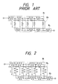
- Fig. 1 schematically shows the state of flow of current I when a voltage is applied to an ECD of the above-explained resistance relationship. Since the vertical resistance of the intermediate layer is smaller than the horizontal resistance of the upper electrode layer, most of the current I flows into the intermediate layer from an end of the upper electrode layer close to the connection electrode. Consequently, in a portion of the ECD close to the connection electrode, the aforementioned reaction proceeds to show faster and denser coloration, whereas in the central portion and in a portion opposite to said connection electrode, the coloration is much slower and paler due to much lower current density.
- an electrochromic device composed of a laminate structure at least of an upper electrode, an electrochromic layer, and a lower electrode
- uniform coloration is achieved (even in a large-size device) by selecting the resistances R 1 , R 2 of the upper and lower electrodes and the internal resistance R 3 of the electrochromic device so as to satisfy relations:
- Fig. 2 shows the state of flow of the current I in the ECD of the present invention, when a voltage is applied across the upper electrode layer (positive side) and the lower electrode layer (negative side).
- the resistances of two electrode layers and the internal resistance of the intermediate layer are so selected as to satisfy the above-mentioned relations: and the current supplied from the connection electrode of the upper electrode layer (in the structure shown in Fig. 2), at first flows in the upper electrode layer without a substantial voltage slope therein, and uniformly flows into the intermediate layer toward the lower electrode layer. Consequently, the voltage across the upper and lower electrode layers is substantially constant in any part of the electrode layers in the horizontal direction.
- Ri, R 2 , and R 3 may satisfy the following condition: which has been experimentally found to promote coloration and erasure of coloration.
- R 3 should be made as large as possible in comparison with R 1 and R 2 , and experimentally preferred is a condition: or more preferably:
- the relationship of the resistances R, , R 2 of the electrode layers is not important. If both layers are transparent electrodes, the resistance of the uppermost electrode layer tends to become larger, in practical film formation, than that of the electrode layer formed directly on the substrate.
- the laminate structure of the ECD of the present invention is only required to have an upper electrode layer, an electrochromic layer and a lower electrode layer.
- a totally solid thin film structure composed of four layers such as electrode layer/electrochromic layer/ion conductive layer/electrode layer or five layers such as electrode layer/reduction coloring electrochromic layer/ion conductive layer/reversible electrolytic oxidation layer/electrode layer.
- the transparent electrode can be formed, for example, of Sn0 2 , ln 2 0 3 , or ITO.
- Such electrode layer can be generally formed by a vacuum thin film deposition technique such as vacuum evaporation, ion plating or sputtering.
- the reduction coloring electrochromic layer can be generally composed of W0 3 or MoOs.
- the ion conductive layer can be composed, for example, of silicon oxide, tantalum oxide, titanium oxide, aluminum oxide, niobium oxide, zirconium oxide, hafnium oxide, lanthanum oxide or magnesium fluoride.
- the thin film of such materials is insulating to electrons depending on the method of film preparation, but is conductive to protons (H + ) and hydroxyl ions (OH-).
- the coloring and color erasing reactions of the electrochromic layer require cations, so that H + ions or Li + ions have to be incorporated in the electrochromic or other layer.
- the H + ions need not necessarily be present from the beginning but can be generated under the voltage application, and water may be added instead of H + ions. The amount of water can be very small, and the coloring and color erasing reactions may take place even by moisture spontaneously entering from the air.
- electrochromic layer and the ion conductive layer may be placed above the other. Furthermore, there may be provided a reversible electrolytic oxidation layer (constituting an oxidation coloring electrochromic layer) or a catalytic layer in opposed relation to the electrochromic layer across the ion conductive layer.
- Such layer may be composed, for example, of oxide or hydroxide of iridium, nickel, chromium, vanadium, ruthenium or rhodium. Such materials may be dispersed in the ion conductive layer or in the transparent electrode, or may be used for dispersing the material of said layers therein.
- the opaque electrode layer may also serve as a reflective layer, and can be composed of a metal such as gold, silver, aluminum, chromium, tin, zinc, nickel, rutenium, rhodium or stainless steel.
- the upper and lower electrode layers have to be connected to external wirings for charge (current) supply.
- a connection electrode of low resistance is superposed, in an area as large as possible, with (in contact with) the transparent electrode.
- the connection electrode of low resistance is formed as a belt in the peripheral area of the transparent electrode layer.
- Said electrode of low resistance can be composed of the materials for the above-mentioned opaque electrode layer, for example aluminum.
- connection electrode In the use of an opaque electrode which is of low resistance, a part of said electrode can be used as the connection electrode.
- Fig. 3 is a schematic cross-sectional view of an embodiment of the ECD of the present invention, wherein the z-direction corresponds to the direction of thickness of the ECD.
- said ITO electrode layer was split into two portions at an end part thereof by forming a narrow groove, thereby forming a connection part 7 for the upper electrode, and a lower electrode layer 2.
- the groove may be formed by etching or laser beam cutting, for example.
- connection part 7 and lower electrode layer 2 may be formed directly by masked evaporation of ITO.
- a reversible electrolytic oxidation layer 5 consisting of a mixture of iridium oxide and tin oxide
- an ion conductive layer 4 consisting of tantalum oxide
- a reduction coloring electrochromic layer 3 consisting of tungsten oxide.
- the resistivity and ion resistivity of the layers can be varied by suitably selecting the conditions of film formation, such as Ar/0 2 ratio, degree of vacuum, film forming rate, substrate temperature, high-frequency power applied, etc.
- the resistances R 1 , R 2 and R 3 of the layers are calculated as follows: Consequently:
- connection electrodes 8a, 8b external wirings 11 a, 11 b were connected, to two phosphor bronze clips of square-C section of a length of 25 cm (connection electrodes) 8a, 8b, which were then mounted on end portions of the substrate 10 in such a manner that the clip 8a is in contact with the connection part 7 for the upper electrode while the clip 8b is in contact with a part of the lower electrode layer 2.
- the clips 8a, 8b constituting the input and output electrodes are regarded as substantially zero resistance (constant potential in any part).
- the wiring connections to the clips may be by soldering or conductive adhesive, for example.
- the shape and dimension of the clips 8a, 8b are so selected as to be capable of defining the position of a sealing substrate 6 for masking the non-display portion in the peripheral part of the ECD.
- the sealing glass substrate 6, coated with epoxy sealing resin 9, was superposed on an area between the clips 8a, 8b and the sealing resin was hardened to complete the ECD of the present embodiment.
- a coloring voltage (+3 V) was applied, by a power source 12, across the upper and lower electrode layers 1, 2 of thus prepared ECD, whereby the ECD showed rapid and uniform coloration over the entire surface, reducing the transmittance of the light of 633 nm to 10 % after 20 seconds.
- the transmittance remained in this state for some time even after the termination of voltage application, and was elevated to 70 % after application of an erasing voltage (-3 V) for 20 seconds.
- this ECD showed uneven coloration and color erasure.
- Fig. 4 is a plan view of a part of the ECD shown in Fig. 3, seen along the Z-axis from above the upper electrode layer 1.
- the structure shown in Fig. 4 is partly different from what is shown in Fig. 3.
- an area 22 indicates the remaining part of the lower electrode 2, excluding the area 21.
Description
- The present invention relates to an electrochromic device capable of uniform coloring.
- A phenomenon of reversible coloration by reversible electrolytic oxidation or reduction under voltage application is called electrochromism.
- Various attempts have been made, since more than 20 years ago, to prepare electrochromic devices (ECD) utilizing an electrochromic material showing such electrochromic phenomenon and capable of coloration and color erasure by voltage application, and to utilize such ECD for a light control device such as an anti-glare mirror, or a 7-segment numeric display unit.
- For example, U.S. Patent No. 3,829,196 discloses a totally solid-state ECD composed of a transparent electrode film (cathode), a tungsten trioxide film, an insulating film, for example of silicon dioxide, and an electrode film (anode) laminated in succession on a glass substrate.
- The tungsten trioxide (W03) film is colored blue when a voltage is applied to said ECD, and returns to the colorless state when an inverse voltage is applied. The mechanism of the coloration and color erasure is not fully understood, but it is theorized that the coloration and color erasure of W03 is governed by a small amount of water present in the W03 film and the insulating film (ion conductive layer).
- The reaction formulae are theorized as follows:


- Also, there is already known an ECD composed of an electrochromic layer capable of coloration by reduction (for example W03), an ion conductive layer, and a layer capable of reversible electrolytic oxidation (for example, iridium oxide or iridium hydroxide) laminated in succession between an upper electrode and a lower electrode for applying a predetermined voltage.
- At least one of the electrode layers directly or indirectly sandwiching the electrochromic layer has to be transparent in order to show the coloration and color erasure to the exterior, and both electrode layers have to be transparent in case of a transmissive ECD.
- It is already known that a transparent electrode can be prepared from Sn02, ln203, ITO (Sn02 - ln203 mixture) or ZnO, for example, but these materials are of relatively low transparency and have to be made thin. Because of this fact, and also because of other considerations, the ECD is usually formed on a substrate such as a glass plate or a plastic plate.
- Also, for certain applications, a sealing substrate for protecting the device is positioned opposite to the substrate of the device, and the device is sealed with epoxy resin, for example.
- The conventional ECD's have been subject to a significant drawback in that the coloration is very slow and is not uniform, and said uneven coloration is particularly pronounced in a large-sized ECD.
- European patent application EP-A2-0 304 198, published after the priority date of the present application, describes an electrochromic device comprising two transparent layers acting as terminal electrodes, between which is disposed a layer of electrochromic material and an auxiliary layer having a large normal resistance compared to the lateral resistance of the adjacent terminal electrode layer. The auxiliary layer is stated to improve the lateral uniformity of the potential applied to the electrochemical cell.
- It would be desirable to provide an ECD capable of showing uniform coloration even in a large size.
- The above-mentioned desideratum can be attained, according to the present invention, by a certain relationship of the resistances of the intermediate layer including the electrochromic layer, and the upper and lower electrodes sandwiching said intermediate layer.
- In accordance with a first aspect of the present invention there is provided an electrochromic device comprising:
- a first electrode layer;
- an intermediate layer including an electrochromic layer;
- a second electrode layer, said first electrode layer, said intermediate layer and said second electrode layer being laminated in succession; and
- an electrode member connected to one of said first and second electrode layers and extending in a predetermined direction transverse to the direction of succession of lamination of said first electrode layer, said intermediate layer (3,4,5) and said second electrode layer;
- wherein the resistances respectively of said first and second electrode layers and the internal resistance of said intermediate layer satisfy following condition:


- pj : resistivity of said first electrode layer;
- P2: resistivity of said second electrode layer;
- P3: ion resistivity of said intermediate layer;
- di : thickness of said first electrode layer;
- d2: thickness of said second electrode layer;
- d3: thickness of said intermediate layer;
- ℓ : shortest of respective lengths, in said predetermined direction, of the electrode layer other than said one electrode layer, said electrode member and said intermediate layer; and
- S superposed area of said first electrode layer, said intermediate layer and said second electrode layer, as viewed along a direction generally perpendicular to the said layers.
- In accordance with a second aspect of the present invention there is provided an electrochromic device comprising:
- a first electrode layer;
- an intermediate layer including an electrochromic layer;
- a second electrode layer, said first electrode layer, said intermediate layer and said second electrode layer being laminated in succession; and
- an electrode member connected to one of said first and second electrode layers and extending in a predetermined direction transverse to the direction of succession of lamination of said first electrode layer, said intermediate layer and said second electrode layer;
- wherein the resistances and respectively of said first and second electrode layers and the internal resistance of said intermediate layer satisfy following conditions:


- pj : resistivity of said first electrode layer;
- P2: resistivity of said second electrode layer;
- ρ3: ion resistivity of said intermediate layer;
- di : thickness of said first electrode layer;
- d2: thickness of said second electrode layer;
- d3: thickness of said intermediate layer;
- ℓ: shortest of respective lengths; in said predetermined direction, of the electrode layer other than said one electrode layer, said electrode member and said intermediate layer; and
- S: superposed area of said first electrode layer, said intermediate layer and said second electrode layer, as viewed along a direction generally perpendicular to the said layers.
-
- Fig. 1 is a schematic view showing the current flow in an ECD, for explaining the principle of the present invention;
- Fig. 2 is a schematic view showing the current flow in an ECD embodying the present invention;
- Fig. 3 is a schematic cross-sectional view of an ECD embodying the present invention; and
- Fig. 4 is a plan view of an ECD for explaining the definition of conditions of the present invention.
- In the following there will be explained the principle of the present invention.
- At first explained is the relationship of the resistances of the intermediate layer, including the electrochromic layer, and the upper and lower electrodes sandwiching said intermediate layer, in a conventional ECD.
- In the conventional ECD, the resistance R1 of the upper electrode layer, the resistance R2 of the lower electrode layer and the internal resistance R3 of the intermediate layer sandwiched between said electrode layers satisfy following relation (1):

- The resistances R1 , R2 and R3 are defined as follows:


- pj : resistivity of upper electrode layer;
- P2: resistivity of lower electrode layer;
- P3: ion resistivity of intermediate layer;
- di : thickness of upper electrode layer;
- d2: thickness of lower electrode layer;
- d3: thickness of intermediate layer;
- ℓ : shortest of the lengths, in the extending direction of connection electrode, of the upper or lower electrode layer connected to said connection electrode, the connection electrode and the intermediate layer; and
- S : superposed area of the upper electrode layer, the intermediate layer and the lower electrode layer, when seen from the direction of lamination thereof.
- It is also assumed that the resistance of the connection electrode is approximately zero, which means following conditions apply:

- P4: resistivity of connection electrode; and
- d4: thickness of connection electrode.
- Fig. 1 schematically shows the state of flow of current I when a voltage is applied to an ECD of the above-explained resistance relationship. Since the vertical resistance of the intermediate layer is smaller than the horizontal resistance of the upper electrode layer, most of the current I flows into the intermediate layer from an end of the upper electrode layer close to the connection electrode. Consequently, in a portion of the ECD close to the connection electrode, the aforementioned reaction proceeds to show faster and denser coloration, whereas in the central portion and in a portion opposite to said connection electrode, the coloration is much slower and paler due to much lower current density.
- This phenomenon results in uneven coloration, which is more pronounced in a large-sized ECD.
- Also, the erasure of coloration proceeds unevenly for the same reason, though the extent of unevenness is less pronounced than in the coloration phase.
- According to one preferred mode of the present invention, in an electrochromic device composed of a laminate structure at least of an upper electrode, an electrochromic layer, and a lower electrode, uniform coloration is achieved (even in a large-size device) by selecting the resistances R1 , R2 of the upper and lower electrodes and the internal resistance R3 of the electrochromic device so as to satisfy relations:


- Fig. 2 shows the state of flow of the current I in the ECD of the present invention, when a voltage is applied across the upper electrode layer (positive side) and the lower electrode layer (negative side).
- Since the resistances of two electrode layers and the internal resistance of the intermediate layer are so selected as to satisfy the above-mentioned relations:


- According to another preferred mode of the invention, Ri, R2, and R3 may satisfy the following condition:

- For achieving more uniform coloration, R3 should be made as large as possible in comparison with R1 and R2, and experimentally preferred is a condition:


- In the present invention, the relationship of the resistances R, , R2 of the electrode layers is not important. If both layers are transparent electrodes, the resistance of the uppermost electrode layer tends to become larger, in practical film formation, than that of the electrode layer formed directly on the substrate.
- The laminate structure of the ECD of the present invention is only required to have an upper electrode layer, an electrochromic layer and a lower electrode layer. There may be employed, for example, a structure including a liquid electrochromic layer, an intermediate layer containing liquid electrolyte, a structure employing an organic electrochromic material or a structure utilizing metal ions such as lithium ions instead protons. However, there is preferred a totally solid thin film structure composed of four layers such as electrode layer/electrochromic layer/ion conductive layer/electrode layer or five layers such as electrode layer/reduction coloring electrochromic layer/ion conductive layer/reversible electrolytic oxidation layer/electrode layer.
- The transparent electrode can be formed, for example, of Sn02, ln203, or ITO. Such electrode layer can be generally formed by a vacuum thin film deposition technique such as vacuum evaporation, ion plating or sputtering.
- The reduction coloring electrochromic layer can be generally composed of W03 or MoOs.
- The ion conductive layer can be composed, for example, of silicon oxide, tantalum oxide, titanium oxide, aluminum oxide, niobium oxide, zirconium oxide, hafnium oxide, lanthanum oxide or magnesium fluoride. The thin film of such materials is insulating to electrons depending on the method of film preparation, but is conductive to protons (H+) and hydroxyl ions (OH-).
- The coloring and color erasing reactions of the electrochromic layer require cations, so that H+ ions or Li+ ions have to be incorporated in the electrochromic or other layer. The H+ ions need not necessarily be present from the beginning but can be generated under the voltage application, and water may be added instead of H+ ions. The amount of water can be very small, and the coloring and color erasing reactions may take place even by moisture spontaneously entering from the air.
- It is possible to place either of the electrochromic layer and the ion conductive layer above the other. Furthermore, there may be provided a reversible electrolytic oxidation layer (constituting an oxidation coloring electrochromic layer) or a catalytic layer in opposed relation to the electrochromic layer across the ion conductive layer.
- Such layer may be composed, for example, of oxide or hydroxide of iridium, nickel, chromium, vanadium, ruthenium or rhodium. Such materials may be dispersed in the ion conductive layer or in the transparent electrode, or may be used for dispersing the material of said layers therein. The opaque electrode layer may also serve as a reflective layer, and can be composed of a metal such as gold, silver, aluminum, chromium, tin, zinc, nickel, rutenium, rhodium or stainless steel.
- The upper and lower electrode layers have to be connected to external wirings for charge (current) supply. In the use of a transparent electrode which is higher in resistance than the external wirings a connection electrode of low resistance is superposed, in an area as large as possible, with (in contact with) the transparent electrode. Normally, the connection electrode of low resistance is formed as a belt in the peripheral area of the transparent electrode layer. Said electrode of low resistance can be composed of the materials for the above-mentioned opaque electrode layer, for example aluminum.
- In the use of an opaque electrode which is of low resistance, a part of said electrode can be used as the connection electrode.
- Fig. 3 is a schematic cross-sectional view of an embodiment of the ECD of the present invention, wherein the z-direction corresponds to the direction of thickness of the ECD.
- At first on the entire surface of a rectangular or parallelogram glass substrate 10 (25 x 15 cm; area S = 375 cm2; length ℓ of connection electrodes for the upper and lower electrode layers = 25 cm) there was formed an ITO electrode layer of a thickness d2 = 2 x 10⁻⁵ cm (resistivity p2 = 2 x 10⁻⁴ Q cm).
- Then said ITO electrode layer was split into two portions at an end part thereof by forming a narrow groove, thereby forming a
connection part 7 for the upper electrode, and alower electrode layer 2. The groove may be formed by etching or laser beam cutting, for example. - Said
connection part 7 andlower electrode layer 2 may be formed directly by masked evaporation of ITO. - On said
lower electrode layer 2, there were formed, in succession, a reversibleelectrolytic oxidation layer 5 consisting of a mixture of iridium oxide and tin oxide, an ionconductive layer 4 consisting of tantalum oxide, and a reductioncoloring electrochromic layer 3 consisting of tungsten oxide. - The intermediate layer, consisting of the above-mentioned three
layers - On the
electrochromic layer 3, there was formed, by evaporation, an ITO electrode layer of a thickness di = 2 x 10⁻⁵ cm (resistivity ρ1 = 4 x 10⁻⁴ Ω. cm) as anupper electrode layer 1. Said ITO layer was formed so as to contact, at an end thereof, with theconnection part 7 formed on thesubstrate 10. - The resistivity and ion resistivity of the layers can be varied by suitably selecting the conditions of film formation, such as Ar/02 ratio, degree of vacuum, film forming rate, substrate temperature, high-frequency power applied, etc.
- The resistances R1 , R2 and R3 of the layers are calculated as follows:


- Thus the condition 4 (Ri + R2) < R3 < 5(Ri + R2) is satisfied.
- Then
external wirings substrate 10 in such a manner that theclip 8a is in contact with theconnection part 7 for the upper electrode while theclip 8b is in contact with a part of thelower electrode layer 2. In this case, theclips - The shape and dimension of the
clips substrate 6 for masking the non-display portion in the peripheral part of the ECD. - Finally, the sealing
glass substrate 6, coated withepoxy sealing resin 9, was superposed on an area between theclips power source 12, across the upper andlower electrode layers - The transmittance remained in this state for some time even after the termination of voltage application, and was elevated to 70 % after application of an erasing voltage (-3 V) for 20 seconds.
- For purposes of comparison, another ECD of same dimensions and thicknesses was prepared with modified resistivity pi, p2 and ion resistivity ρ3 of the layers. Resistances were R1 = 12 Ω , R2 = 6 Ω , and R3 = 0.15 Ω , so that:

- In the same test as conducted with the foregoing embodiment, this ECD showed uneven coloration and color erasure.
- Now reference is made to Fig. 4 for explaining the definition of S and 1.
- Fig. 4 is a plan view of a part of the ECD shown in Fig. 3, seen along the Z-axis from above the
upper electrode layer 1. For explaining the definition of S and ℓ , the structure shown in Fig. 4 is partly different from what is shown in Fig. 3. - S corresponds to the superposed area, when seen along z-axis, of the
upper electrode 1, theintermediate layers lower electrode 2. In the structure shown in Fig. 4, thearea 21 of thelower electrode 2 is smallest among these. Consequently, the area S corresponds to thearea 21 of thelower electrode 2. If the area of theintermediate layers upper electrode 1, theintermediate layers lower electrode 2, the area S would correspond to the area of said intermediate layers. In Fig. 4, anarea 22 indicates the remaining part of thelower electrode 2, excluding thearea 21. - 1 corresponds to the shortest of the
length 11 of theconnection electrode 7 in the x-direction, the length ℓ3 of thelower electrode 2 in the x-direction, and thelength 12 of theintermediate layers
Claims (8)


Applications Claiming Priority (4)
| Application Number | Priority Date | Filing Date | Title |
|---|---|---|---|
| JP203285/88 | 1988-08-17 | ||
| JP63203285A JPH0253034A (en) | 1988-08-17 | 1988-08-17 | Electrochromic element |
| JP28970/89 | 1989-02-08 | ||
| JP1028970A JP2827247B2 (en) | 1989-02-08 | 1989-02-08 | Electrochromic element that uniformly colors |
Publications (4)
| Publication Number | Publication Date |
|---|---|
| EP0356099A2 EP0356099A2 (en) | 1990-02-28 |
| EP0356099A3 EP0356099A3 (en) | 1990-07-25 |
| EP0356099B1 true EP0356099B1 (en) | 1994-05-18 |
| EP0356099B2 EP0356099B2 (en) | 1998-03-11 |
Family
ID=26367122
Family Applications (1)
| Application Number | Title | Priority Date | Filing Date |
|---|---|---|---|
| EP89308231A Expired - Lifetime EP0356099B2 (en) | 1988-08-17 | 1989-08-14 | Electrochromic device |
Country Status (5)
| Country | Link |
|---|---|
| US (1) | US5148306A (en) |
| EP (1) | EP0356099B2 (en) |
| KR (1) | KR0128732B1 (en) |
| CA (1) | CA1313562C (en) |
| DE (1) | DE68915368T3 (en) |
Cited By (7)
| Publication number | Priority date | Publication date | Assignee | Title |
|---|---|---|---|---|
| US7824045B2 (en) | 2007-05-23 | 2010-11-02 | Donnelly Corporation | Exterior mirror element with wide angle portion |
| US7934843B2 (en) | 2003-05-20 | 2011-05-03 | Donnelly Corporation | Exterior sideview mirror system |
| US8102279B2 (en) | 2007-11-05 | 2012-01-24 | Magna Mirrors Of America, Inc. | Exterior mirror with indicator |
| US8242896B2 (en) | 2006-10-24 | 2012-08-14 | Donnelly Corporation | Vehicle exterior rearview mirror system with a highly viewable display indicator for the driver |
| US8988755B2 (en) | 2011-05-13 | 2015-03-24 | Magna Mirrors Of America, Inc. | Mirror reflective element |
| US9205780B2 (en) | 2010-02-04 | 2015-12-08 | Magna Mirrors Of America, Inc. | Electro-optic rearview mirror assembly for vehicle |
| US9290970B2 (en) | 2011-11-14 | 2016-03-22 | Magna Mirrors Of America, Inc. | Door handle system for vehicle |
Families Citing this family (59)
| Publication number | Priority date | Publication date | Assignee | Title |
|---|---|---|---|---|
| DE4006947A1 (en) * | 1990-03-06 | 1991-09-12 | Bayerische Motoren Werke Ag | METHOD AND ARRANGEMENT FOR APPLYING AN ELECTRICAL OPERATING VOLTAGE TO AN ELECTROOPTIC LAYER SYSTEM |
| DE4121385A1 (en) * | 1991-06-28 | 1993-01-07 | Bayerische Motoren Werke Ag | Electro=optical layer system for heating vehicle windscreen - uses conductor layers applied to outside surfaces of opposing control electrodes |
| FR2691550B1 (en) * | 1992-05-21 | 1995-04-21 | Saint Gobain Vitrage Int | Architectural electrochromic glazing. |
| US5504596A (en) * | 1992-12-21 | 1996-04-02 | Nikon Corporation | Exposure method and apparatus using holographic techniques |
| US5910854A (en) | 1993-02-26 | 1999-06-08 | Donnelly Corporation | Electrochromic polymeric solid films, manufacturing electrochromic devices using such solid films, and processes for making such solid films and devices |
| US5657150A (en) * | 1993-09-10 | 1997-08-12 | Eyeonics Corporation | Electrochromic edge isolation-interconnect system, process, and device for its manufacture |
| US5977162A (en) * | 1996-09-16 | 1999-11-02 | Seidman; Michael D. | Therapeutic treatment for auditory function |
| DE19640515A1 (en) * | 1996-10-01 | 1998-04-09 | Flachglas Ag | Electrochromic mirror and method for producing an electrochromic mirror |
| US6326613B1 (en) | 1998-01-07 | 2001-12-04 | Donnelly Corporation | Vehicle interior mirror assembly adapted for containing a rain sensor |
| US8294975B2 (en) | 1997-08-25 | 2012-10-23 | Donnelly Corporation | Automotive rearview mirror assembly |
| US6124886A (en) | 1997-08-25 | 2000-09-26 | Donnelly Corporation | Modular rearview mirror assembly |
| US6172613B1 (en) | 1998-02-18 | 2001-01-09 | Donnelly Corporation | Rearview mirror assembly incorporating vehicle information display |
| US8288711B2 (en) | 1998-01-07 | 2012-10-16 | Donnelly Corporation | Interior rearview mirror system with forwardly-viewing camera and a control |
| US6445287B1 (en) | 2000-02-28 | 2002-09-03 | Donnelly Corporation | Tire inflation assistance monitoring system |
| US6477464B2 (en) | 2000-03-09 | 2002-11-05 | Donnelly Corporation | Complete mirror-based global-positioning system (GPS) navigation solution |
| US6693517B2 (en) | 2000-04-21 | 2004-02-17 | Donnelly Corporation | Vehicle mirror assembly communicating wirelessly with vehicle accessories and occupants |
| US6329925B1 (en) | 1999-11-24 | 2001-12-11 | Donnelly Corporation | Rearview mirror assembly with added feature modular display |
| US6130448A (en) * | 1998-08-21 | 2000-10-10 | Gentex Corporation | Optical sensor package and method of making same |
| JP2000292818A (en) * | 1999-04-07 | 2000-10-20 | Fuji Photo Film Co Ltd | Optical writing display element and optical writing display device using the same |
| US7167796B2 (en) | 2000-03-09 | 2007-01-23 | Donnelly Corporation | Vehicle navigation system for use with a telematics system |
| US7855755B2 (en) | 2005-11-01 | 2010-12-21 | Donnelly Corporation | Interior rearview mirror assembly with display |
| US7370983B2 (en) | 2000-03-02 | 2008-05-13 | Donnelly Corporation | Interior mirror assembly with display |
| WO2001064481A2 (en) | 2000-03-02 | 2001-09-07 | Donnelly Corporation | Video mirror systems incorporating an accessory module |
| JP3425693B2 (en) * | 2000-05-22 | 2003-07-14 | 株式会社村上開明堂 | EC mirror electrode structure |
| EP1333316A4 (en) * | 2000-11-10 | 2004-04-07 | Murakami Corp | Solid state electrochromic element and mirror device and crt display comprising it |
| US7581859B2 (en) | 2005-09-14 | 2009-09-01 | Donnelly Corp. | Display device for exterior rearview mirror |
| US7255451B2 (en) | 2002-09-20 | 2007-08-14 | Donnelly Corporation | Electro-optic mirror cell |
| DE60220379T2 (en) | 2001-01-23 | 2008-01-24 | Donnelly Corp., Holland | IMPROVED VEHICLE LIGHTING SYSTEM |
| US6918674B2 (en) | 2002-05-03 | 2005-07-19 | Donnelly Corporation | Vehicle rearview mirror system |
| EP1514246A4 (en) | 2002-06-06 | 2008-04-16 | Donnelly Corp | Interior rearview mirror system with compass |
| US7329013B2 (en) | 2002-06-06 | 2008-02-12 | Donnelly Corporation | Interior rearview mirror system with compass |
| US7649674B2 (en) * | 2002-06-10 | 2010-01-19 | E Ink Corporation | Electro-optic display with edge seal |
| WO2004026633A2 (en) | 2002-09-20 | 2004-04-01 | Donnelly Corporation | Mirror reflective element assembly |
| US7360932B2 (en) | 2004-06-01 | 2008-04-22 | Donnelly Corporation | Mirror assembly for vehicle |
| US7310177B2 (en) | 2002-09-20 | 2007-12-18 | Donnelly Corporation | Electro-optic reflective element assembly |
| AU2003287535A1 (en) * | 2002-11-05 | 2004-06-07 | Donnelly Corporation | Electro-optic reflective element assembly |
| JP4101864B2 (en) * | 2002-11-18 | 2008-06-18 | 株式会社村上開明堂 | Solid EC element |
| US7446924B2 (en) | 2003-10-02 | 2008-11-04 | Donnelly Corporation | Mirror reflective element assembly including electronic component |
| US7308341B2 (en) | 2003-10-14 | 2007-12-11 | Donnelly Corporation | Vehicle communication system |
| WO2005062966A2 (en) * | 2003-12-23 | 2005-07-14 | Donnelly Corporation | Electro-optic mirror cell |
| DE102004005611B4 (en) * | 2004-02-05 | 2006-04-27 | Saint-Gobain Sekurit Deutschland Gmbh & Co. Kg | Transparent pane with partially darkenable field of view and method for controlling an electrochromically discolourable surface element in a transparent pane, in particular a windshield |
| US7400435B2 (en) | 2005-01-19 | 2008-07-15 | Donnelly Corporation | Mirror assembly with heater element |
| US7626749B2 (en) | 2005-05-16 | 2009-12-01 | Donnelly Corporation | Vehicle mirror assembly with indicia at reflective element |
| US11242009B2 (en) | 2005-07-06 | 2022-02-08 | Donnelly Corporation | Vehicular exterior mirror system with blind spot indicator |
| US11498487B2 (en) | 2005-07-06 | 2022-11-15 | Magna Mirrors Of America, Inc. | Vehicular exterior mirror system with blind spot indicator |
| KR100756846B1 (en) * | 2005-11-02 | 2007-09-07 | 주식회사 엘지화학 | Electrode structure of electrochromic device |
| US11890991B2 (en) | 2006-10-24 | 2024-02-06 | Magna Mirrors Of America, Inc. | Vehicular exterior rearview mirror assembly with blind spot indicator element |
| US8154418B2 (en) | 2008-03-31 | 2012-04-10 | Magna Mirrors Of America, Inc. | Interior rearview mirror system |
| US7813023B2 (en) | 2008-06-09 | 2010-10-12 | Magna Mirrors Of America, Inc. | Electro-optic mirror |
| US8514476B2 (en) | 2008-06-25 | 2013-08-20 | View, Inc. | Multi-pane dynamic window and method for making same |
| US7719751B2 (en) * | 2008-09-17 | 2010-05-18 | Soladigm, Inc. | Electrical contact technique for electrochromic windows |
| US10429712B2 (en) | 2012-04-20 | 2019-10-01 | View, Inc. | Angled bus bar |
| US8736940B2 (en) | 2011-09-30 | 2014-05-27 | Magna Mirrors Of America, Inc. | Exterior mirror with integral spotter mirror and method of making same |
| US11635666B2 (en) | 2012-03-13 | 2023-04-25 | View, Inc | Methods of controlling multi-zone tintable windows |
| US9341912B2 (en) | 2012-03-13 | 2016-05-17 | View, Inc. | Multi-zone EC windows |
| TWI685706B (en) | 2013-06-18 | 2020-02-21 | 唯景公司 | Electrochromic devices on non-rectangular shapes |
| US10442360B2 (en) | 2017-03-02 | 2019-10-15 | Magna Mirrors Of America, Inc. | Interior rearview mirror assembly with display and tilt mechanism |
| US10739662B2 (en) * | 2017-03-03 | 2020-08-11 | Leaphigh Inc. | Electrochromic element and electrochromic device including the same |
| EP3712694A1 (en) * | 2019-03-19 | 2020-09-23 | Ricoh Company, Ltd. | Electronic device, method for producing electronic device, photochromatic lens unit, and electrochromic element |
Family Cites Families (3)
| Publication number | Priority date | Publication date | Assignee | Title |
|---|---|---|---|---|
| US3829196A (en) * | 1971-01-27 | 1974-08-13 | American Cyanamid Co | Variable light transmission device |
| JPS58129422A (en) * | 1982-01-28 | 1983-08-02 | Asahi Glass Co Ltd | Dimmer |
| FR2601150B1 (en) * | 1986-07-04 | 1991-05-31 | Saint Gobain Vitrage | VARIABLE TRANSMISSION GLAZING OF THE ELECTROCHROME TYPE |
-
1989
- 1989-08-10 CA CA000608011A patent/CA1313562C/en not_active Expired - Fee Related
- 1989-08-14 DE DE68915368T patent/DE68915368T3/en not_active Expired - Lifetime
- 1989-08-14 EP EP89308231A patent/EP0356099B2/en not_active Expired - Lifetime
- 1989-08-16 KR KR1019890011628A patent/KR0128732B1/en not_active IP Right Cessation
-
1991
- 1991-11-21 US US07/798,368 patent/US5148306A/en not_active Expired - Lifetime
Cited By (27)
| Publication number | Priority date | Publication date | Assignee | Title |
|---|---|---|---|---|
| US8550642B2 (en) | 2003-05-20 | 2013-10-08 | Donnelly Corporation | Exterior rearview mirror assembly |
| US7934843B2 (en) | 2003-05-20 | 2011-05-03 | Donnelly Corporation | Exterior sideview mirror system |
| US8562157B2 (en) | 2003-05-20 | 2013-10-22 | Donnelly Corporation | Extended field of view exterior mirror element for vehicle |
| US8591047B2 (en) | 2003-05-20 | 2013-11-26 | Donnelly Corporation | Exterior sideview mirror assembly |
| US8128244B2 (en) | 2003-05-20 | 2012-03-06 | Donnelly Corporation | Exterior sideview mirror system |
| US8128243B2 (en) | 2003-05-20 | 2012-03-06 | Donnelly Corporation | Exterior sideview mirror system |
| US8147077B2 (en) | 2003-05-20 | 2012-04-03 | Donnelly Corporation | Exterior sideview mirror system |
| US8899762B2 (en) | 2003-05-20 | 2014-12-02 | Donnelly Corporation | Vehicular exterior sideview mirror system with extended field of view |
| US8267534B2 (en) | 2003-05-20 | 2012-09-18 | Donnelly Corporation | Exterior rearview mirror assembly |
| US8783882B2 (en) | 2003-05-20 | 2014-07-22 | Donnelly Corporation | Extended field of view exterior mirror element for vehicle |
| US9340161B2 (en) | 2003-05-20 | 2016-05-17 | Donnelly Corporation | Extended field of view exterior mirror element for vehicle |
| US9035754B2 (en) | 2005-07-06 | 2015-05-19 | Donnelly Corporation | Vehicle exterior rearview mirror system having an indicator at a back plate of an exterior rearview mirror assembly |
| US9302624B2 (en) | 2005-07-06 | 2016-04-05 | Donnelly Corporation | Vehicle exterior rearview mirror system having an indicator at a back plate of an exterior rearview mirror assembly |
| US8466779B2 (en) | 2006-10-24 | 2013-06-18 | Donnelly Corporation | Vehicle exterior rearview mirror system with a highly viewable display indicator for the driver |
| US8525697B2 (en) | 2006-10-24 | 2013-09-03 | Magna Mirrors Of America, Inc. | Exterior mirror reflective element sub-assembly with signal indicator |
| US8242896B2 (en) | 2006-10-24 | 2012-08-14 | Donnelly Corporation | Vehicle exterior rearview mirror system with a highly viewable display indicator for the driver |
| US9333909B2 (en) | 2006-10-24 | 2016-05-10 | Magna Mirrors Of America, Inc. | Exterior mirror reflective element sub-assembly |
| US9013288B2 (en) | 2006-10-24 | 2015-04-21 | Magna Mirrors Of America, Inc. | Exterior mirror reflective element sub-assembly |
| US9162624B2 (en) | 2006-10-24 | 2015-10-20 | Magna Mirrors Of America, Inc. | Exterior mirror reflective element sub-assembly |
| US7824045B2 (en) | 2007-05-23 | 2010-11-02 | Donnelly Corporation | Exterior mirror element with wide angle portion |
| US7887204B2 (en) | 2007-05-23 | 2011-02-15 | Donnelly Corporation | Exterior mirror element with wide angle portion |
| US8305235B2 (en) | 2007-11-05 | 2012-11-06 | Magna Mirrors Of America, Inc. | Exterior mirror reflective element sub-assembly with signal indicator |
| US8102279B2 (en) | 2007-11-05 | 2012-01-24 | Magna Mirrors Of America, Inc. | Exterior mirror with indicator |
| US9205780B2 (en) | 2010-02-04 | 2015-12-08 | Magna Mirrors Of America, Inc. | Electro-optic rearview mirror assembly for vehicle |
| US9290127B2 (en) | 2011-05-13 | 2016-03-22 | Magna Mirrors Of America, Inc. | Mirror reflective element |
| US8988755B2 (en) | 2011-05-13 | 2015-03-24 | Magna Mirrors Of America, Inc. | Mirror reflective element |
| US9290970B2 (en) | 2011-11-14 | 2016-03-22 | Magna Mirrors Of America, Inc. | Door handle system for vehicle |
Also Published As
| Publication number | Publication date |
|---|---|
| EP0356099B2 (en) | 1998-03-11 |
| KR900003665A (en) | 1990-03-26 |
| DE68915368T2 (en) | 1994-11-03 |
| DE68915368D1 (en) | 1994-06-23 |
| EP0356099A3 (en) | 1990-07-25 |
| DE68915368T3 (en) | 1998-06-10 |
| KR0128732B1 (en) | 1998-04-04 |
| US5148306A (en) | 1992-09-15 |
| CA1313562C (en) | 1993-02-09 |
| EP0356099A2 (en) | 1990-02-28 |
Similar Documents
| Publication | Publication Date | Title |
|---|---|---|
| EP0356099B1 (en) | Electrochromic device | |
| JP2696827B2 (en) | Driving method of electrochromic device | |
| US4824221A (en) | Electrochromic device | |
| US5066111A (en) | Electrochromic window with integrated bus bars | |
| JP3308033B2 (en) | Electrochromic window glass | |
| JPH0243162B2 (en) | ||
| US4940315A (en) | Patterning of insulator on electrochromic material as determinant for area of coloration | |
| JPH0728099A (en) | Fully solid state type electrochromic element and its production | |
| JPS62143032A (en) | Light dimming body | |
| JP2827247B2 (en) | Electrochromic element that uniformly colors | |
| JPH06167724A (en) | Production of light control glass | |
| JPS6186733A (en) | Electrochromic element | |
| JPH0820648B2 (en) | EC device with extraction electrodes on the end face | |
| JP2567786Y2 (en) | Electrochromic device | |
| JPH0522919Y2 (en) | ||
| JPH0128927B2 (en) | ||
| JPH07140494A (en) | Electrochromic element | |
| JP2000047265A (en) | Electrochromic anti-dazzle mirror | |
| JPH11242246A (en) | Electrochromic element and its production | |
| JPH10197907A (en) | Electrochromic element | |
| JPH0253034A (en) | Electrochromic element | |
| JP2600830B2 (en) | Electrochromic element with increased weather resistance | |
| JPS62150233A (en) | Electrochromic display element | |
| JP2725352B2 (en) | Electrochromic device | |
| JPH0740977Y2 (en) | Electrochromic device having conductive clip terminal |
Legal Events
| Date | Code | Title | Description |
|---|---|---|---|
| PUAI | Public reference made under article 153(3) epc to a published international application that has entered the european phase |
Free format text: ORIGINAL CODE: 0009012 |
|
| AK | Designated contracting states |
Kind code of ref document: A2 Designated state(s): DE FR GB IT |
|
| PUAL | Search report despatched |
Free format text: ORIGINAL CODE: 0009013 |
|
| AK | Designated contracting states |
Kind code of ref document: A3 Designated state(s): DE FR GB IT |
|
| 17P | Request for examination filed |
Effective date: 19901212 |
|
| 17Q | First examination report despatched |
Effective date: 19920925 |
|
| GRAA | (expected) grant |
Free format text: ORIGINAL CODE: 0009210 |
|
| AK | Designated contracting states |
Kind code of ref document: B1 Designated state(s): DE FR GB IT |
|
| ITF | It: translation for a ep patent filed |
Owner name: SOCIETA' ITALIANA BREVETTI S.P.A. |
|
| REF | Corresponds to: |
Ref document number: 68915368 Country of ref document: DE Date of ref document: 19940623 |
|
| ET | Fr: translation filed | ||
| PLBI | Opposition filed |
Free format text: ORIGINAL CODE: 0009260 |
|
| 26 | Opposition filed |
Opponent name: FLACHGLAS AKTIENGESELLSCHAFT Effective date: 19950216 |
|
| PLBF | Reply of patent proprietor to notice(s) of opposition |
Free format text: ORIGINAL CODE: EPIDOS OBSO |
|
| PLAW | Interlocutory decision in opposition |
Free format text: ORIGINAL CODE: EPIDOS IDOP |
|
| PLAW | Interlocutory decision in opposition |
Free format text: ORIGINAL CODE: EPIDOS IDOP |
|
| ITF | It: translation for a ep patent filed |
Owner name: SOCIETA' ITALIANA BREVETTI S.P.A. |
|
| PUAH | Patent maintained in amended form |
Free format text: ORIGINAL CODE: 0009272 |
|
| STAA | Information on the status of an ep patent application or granted ep patent |
Free format text: STATUS: PATENT MAINTAINED AS AMENDED |
|
| 27A | Patent maintained in amended form |
Effective date: 19980311 |
|
| AK | Designated contracting states |
Kind code of ref document: B2 Designated state(s): DE FR GB IT |
|
| ET3 | Fr: translation filed ** decision concerning opposition | ||
| PGFP | Annual fee paid to national office [announced via postgrant information from national office to epo] |
Ref country code: FR Payment date: 19990810 Year of fee payment: 11 |
|
| PGFP | Annual fee paid to national office [announced via postgrant information from national office to epo] |
Ref country code: GB Payment date: 19990811 Year of fee payment: 11 |
|
| PGFP | Annual fee paid to national office [announced via postgrant information from national office to epo] |
Ref country code: DE Payment date: 19990816 Year of fee payment: 11 |
|
| PG25 | Lapsed in a contracting state [announced via postgrant information from national office to epo] |
Ref country code: GB Free format text: LAPSE BECAUSE OF NON-PAYMENT OF DUE FEES Effective date: 20000814 |
|
| GBPC | Gb: european patent ceased through non-payment of renewal fee |
Effective date: 20000814 |
|
| PG25 | Lapsed in a contracting state [announced via postgrant information from national office to epo] |
Ref country code: FR Free format text: LAPSE BECAUSE OF NON-PAYMENT OF DUE FEES Effective date: 20010430 |
|
| PG25 | Lapsed in a contracting state [announced via postgrant information from national office to epo] |
Ref country code: DE Free format text: LAPSE BECAUSE OF NON-PAYMENT OF DUE FEES Effective date: 20010501 |
|
| REG | Reference to a national code |
Ref country code: FR Ref legal event code: ST |
|
| PG25 | Lapsed in a contracting state [announced via postgrant information from national office to epo] |
Ref country code: IT Free format text: LAPSE BECAUSE OF NON-PAYMENT OF DUE FEES;WARNING: LAPSES OF ITALIAN PATENTS WITH EFFECTIVE DATE BEFORE 2007 MAY HAVE OCCURRED AT ANY TIME BEFORE 2007. THE CORRECT EFFECTIVE DATE MAY BE DIFFERENT FROM THE ONE RECORDED. Effective date: 20050814 |