EP0355522A2 - Solid state image pickup device - Google Patents
Solid state image pickup device Download PDFInfo
- Publication number
- EP0355522A2 EP0355522A2 EP89114371A EP89114371A EP0355522A2 EP 0355522 A2 EP0355522 A2 EP 0355522A2 EP 89114371 A EP89114371 A EP 89114371A EP 89114371 A EP89114371 A EP 89114371A EP 0355522 A2 EP0355522 A2 EP 0355522A2
- Authority
- EP
- European Patent Office
- Prior art keywords
- transparent substrate
- chips
- substrate chips
- photoelectric converting
- converting elements
- Prior art date
- Legal status (The legal status is an assumption and is not a legal conclusion. Google has not performed a legal analysis and makes no representation as to the accuracy of the status listed.)
- Granted
Links
- 239000007787 solid Substances 0.000 title claims abstract description 31
- 239000000758 substrate Substances 0.000 claims abstract description 125
- 239000003795 chemical substances by application Substances 0.000 claims abstract description 34
- 239000000463 material Substances 0.000 claims description 28
- 239000000945 filler Substances 0.000 claims description 21
- 239000011810 insulating material Substances 0.000 claims description 15
- 229920000620 organic polymer Polymers 0.000 claims description 15
- 239000002861 polymer material Substances 0.000 claims description 15
- VYPSYNLAJGMNEJ-UHFFFAOYSA-N Silicium dioxide Chemical compound O=[Si]=O VYPSYNLAJGMNEJ-UHFFFAOYSA-N 0.000 claims description 10
- 229920001296 polysiloxane Polymers 0.000 claims description 9
- 229920002050 silicone resin Polymers 0.000 claims description 8
- 239000004020 conductor Substances 0.000 claims description 7
- 230000007423 decrease Effects 0.000 claims description 6
- 239000002985 plastic film Substances 0.000 claims description 6
- 229920006255 plastic film Polymers 0.000 claims description 4
- 229920013730 reactive polymer Polymers 0.000 claims description 4
- 229920003023 plastic Polymers 0.000 claims description 3
- 230000003287 optical effect Effects 0.000 abstract description 11
- 239000000853 adhesive Substances 0.000 description 12
- 230000001070 adhesive effect Effects 0.000 description 12
- 239000011521 glass Substances 0.000 description 10
- 239000004925 Acrylic resin Substances 0.000 description 7
- 229920000178 Acrylic resin Polymers 0.000 description 7
- 238000000034 method Methods 0.000 description 6
- 239000010453 quartz Substances 0.000 description 6
- XAGFODPZIPBFFR-UHFFFAOYSA-N aluminium Chemical compound [Al] XAGFODPZIPBFFR-UHFFFAOYSA-N 0.000 description 5
- 229910052782 aluminium Inorganic materials 0.000 description 5
- 239000012298 atmosphere Substances 0.000 description 5
- 230000001681 protective effect Effects 0.000 description 5
- NIXOWILDQLNWCW-UHFFFAOYSA-N acrylic acid group Chemical group C(C=C)(=O)O NIXOWILDQLNWCW-UHFFFAOYSA-N 0.000 description 4
- 230000000694 effects Effects 0.000 description 4
- 238000010438 heat treatment Methods 0.000 description 4
- 239000003522 acrylic cement Substances 0.000 description 3
- 239000005388 borosilicate glass Substances 0.000 description 3
- 238000000926 separation method Methods 0.000 description 3
- 229920001187 thermosetting polymer Polymers 0.000 description 3
- 239000004593 Epoxy Substances 0.000 description 2
- 230000003247 decreasing effect Effects 0.000 description 2
- 239000003822 epoxy resin Substances 0.000 description 2
- 230000001788 irregular Effects 0.000 description 2
- 238000004519 manufacturing process Methods 0.000 description 2
- 229920000647 polyepoxide Polymers 0.000 description 2
- 229920005989 resin Polymers 0.000 description 2
- 239000011347 resin Substances 0.000 description 2
- 230000035939 shock Effects 0.000 description 2
- 239000004642 Polyimide Substances 0.000 description 1
- CDBYLPFSWZWCQE-UHFFFAOYSA-L Sodium Carbonate Chemical compound [Na+].[Na+].[O-]C([O-])=O CDBYLPFSWZWCQE-UHFFFAOYSA-L 0.000 description 1
- 239000003513 alkali Substances 0.000 description 1
- 238000010420 art technique Methods 0.000 description 1
- 229910052788 barium Inorganic materials 0.000 description 1
- DSAJWYNOEDNPEQ-UHFFFAOYSA-N barium atom Chemical compound [Ba] DSAJWYNOEDNPEQ-UHFFFAOYSA-N 0.000 description 1
- 238000005452 bending Methods 0.000 description 1
- 230000005540 biological transmission Effects 0.000 description 1
- 239000003990 capacitor Substances 0.000 description 1
- 238000000576 coating method Methods 0.000 description 1
- 238000010276 construction Methods 0.000 description 1
- 238000010586 diagram Methods 0.000 description 1
- 238000002474 experimental method Methods 0.000 description 1
- PCHJSUWPFVWCPO-UHFFFAOYSA-N gold Chemical compound [Au] PCHJSUWPFVWCPO-UHFFFAOYSA-N 0.000 description 1
- 229910052737 gold Inorganic materials 0.000 description 1
- 239000010931 gold Substances 0.000 description 1
- 239000003779 heat-resistant material Substances 0.000 description 1
- 238000003384 imaging method Methods 0.000 description 1
- 239000011256 inorganic filler Substances 0.000 description 1
- 229910003475 inorganic filler Inorganic materials 0.000 description 1
- CNQCVBJFEGMYDW-UHFFFAOYSA-N lawrencium atom Chemical compound [Lr] CNQCVBJFEGMYDW-UHFFFAOYSA-N 0.000 description 1
- 239000007788 liquid Substances 0.000 description 1
- 229910021421 monocrystalline silicon Inorganic materials 0.000 description 1
- 239000004033 plastic Substances 0.000 description 1
- 229920000728 polyester Polymers 0.000 description 1
- -1 polyethylene terephthalate Polymers 0.000 description 1
- 229920000139 polyethylene terephthalate Polymers 0.000 description 1
- 239000005020 polyethylene terephthalate Substances 0.000 description 1
- 229920001721 polyimide Polymers 0.000 description 1
- 239000011253 protective coating Substances 0.000 description 1
- 238000000275 quality assurance Methods 0.000 description 1
- 239000013464 silicone adhesive Substances 0.000 description 1
- 238000005476 soldering Methods 0.000 description 1
- 239000000126 substance Substances 0.000 description 1
- 229920002803 thermoplastic polyurethane Polymers 0.000 description 1
Images


Classifications
-
- H—ELECTRICITY
- H01—ELECTRIC ELEMENTS
- H01L—SEMICONDUCTOR DEVICES NOT COVERED BY CLASS H10
- H01L25/00—Assemblies consisting of a plurality of individual semiconductor or other solid state devices ; Multistep manufacturing processes thereof
- H01L25/03—Assemblies consisting of a plurality of individual semiconductor or other solid state devices ; Multistep manufacturing processes thereof all the devices being of a type provided for in the same subgroup of groups H01L27/00 - H01L33/00, or in a single subclass of H10K, H10N, e.g. assemblies of rectifier diodes
- H01L25/04—Assemblies consisting of a plurality of individual semiconductor or other solid state devices ; Multistep manufacturing processes thereof all the devices being of a type provided for in the same subgroup of groups H01L27/00 - H01L33/00, or in a single subclass of H10K, H10N, e.g. assemblies of rectifier diodes the devices not having separate containers
- H01L25/041—Assemblies consisting of a plurality of individual semiconductor or other solid state devices ; Multistep manufacturing processes thereof all the devices being of a type provided for in the same subgroup of groups H01L27/00 - H01L33/00, or in a single subclass of H10K, H10N, e.g. assemblies of rectifier diodes the devices not having separate containers the devices being of a type provided for in group H01L31/00
- H01L25/042—Assemblies consisting of a plurality of individual semiconductor or other solid state devices ; Multistep manufacturing processes thereof all the devices being of a type provided for in the same subgroup of groups H01L27/00 - H01L33/00, or in a single subclass of H10K, H10N, e.g. assemblies of rectifier diodes the devices not having separate containers the devices being of a type provided for in group H01L31/00 the devices being arranged next to each other
-
- H—ELECTRICITY
- H01—ELECTRIC ELEMENTS
- H01L—SEMICONDUCTOR DEVICES NOT COVERED BY CLASS H10
- H01L27/00—Devices consisting of a plurality of semiconductor or other solid-state components formed in or on a common substrate
- H01L27/14—Devices consisting of a plurality of semiconductor or other solid-state components formed in or on a common substrate including semiconductor components sensitive to infrared radiation, light, electromagnetic radiation of shorter wavelength or corpuscular radiation and specially adapted either for the conversion of the energy of such radiation into electrical energy or for the control of electrical energy by such radiation
- H01L27/144—Devices controlled by radiation
- H01L27/146—Imager structures
- H01L27/148—Charge coupled imagers
- H01L27/14825—Linear CCD imagers
-
- H—ELECTRICITY
- H01—ELECTRIC ELEMENTS
- H01L—SEMICONDUCTOR DEVICES NOT COVERED BY CLASS H10
- H01L31/00—Semiconductor devices sensitive to infrared radiation, light, electromagnetic radiation of shorter wavelength or corpuscular radiation and specially adapted either for the conversion of the energy of such radiation into electrical energy or for the control of electrical energy by such radiation; Processes or apparatus specially adapted for the manufacture or treatment thereof or of parts thereof; Details thereof
- H01L31/02—Details
- H01L31/0203—Containers; Encapsulations, e.g. encapsulation of photodiodes
-
- H—ELECTRICITY
- H01—ELECTRIC ELEMENTS
- H01L—SEMICONDUCTOR DEVICES NOT COVERED BY CLASS H10
- H01L2224/00—Indexing scheme for arrangements for connecting or disconnecting semiconductor or solid-state bodies and methods related thereto as covered by H01L24/00
- H01L2224/01—Means for bonding being attached to, or being formed on, the surface to be connected, e.g. chip-to-package, die-attach, "first-level" interconnects; Manufacturing methods related thereto
- H01L2224/42—Wire connectors; Manufacturing methods related thereto
- H01L2224/44—Structure, shape, material or disposition of the wire connectors prior to the connecting process
- H01L2224/45—Structure, shape, material or disposition of the wire connectors prior to the connecting process of an individual wire connector
- H01L2224/45001—Core members of the connector
- H01L2224/45099—Material
- H01L2224/451—Material with a principal constituent of the material being a metal or a metalloid, e.g. boron (B), silicon (Si), germanium (Ge), arsenic (As), antimony (Sb), tellurium (Te) and polonium (Po), and alloys thereof
- H01L2224/45117—Material with a principal constituent of the material being a metal or a metalloid, e.g. boron (B), silicon (Si), germanium (Ge), arsenic (As), antimony (Sb), tellurium (Te) and polonium (Po), and alloys thereof the principal constituent melting at a temperature of greater than or equal to 400°C and less than 950°C
- H01L2224/45124—Aluminium (Al) as principal constituent
-
- H—ELECTRICITY
- H01—ELECTRIC ELEMENTS
- H01L—SEMICONDUCTOR DEVICES NOT COVERED BY CLASS H10
- H01L2224/00—Indexing scheme for arrangements for connecting or disconnecting semiconductor or solid-state bodies and methods related thereto as covered by H01L24/00
- H01L2224/01—Means for bonding being attached to, or being formed on, the surface to be connected, e.g. chip-to-package, die-attach, "first-level" interconnects; Manufacturing methods related thereto
- H01L2224/42—Wire connectors; Manufacturing methods related thereto
- H01L2224/47—Structure, shape, material or disposition of the wire connectors after the connecting process
- H01L2224/48—Structure, shape, material or disposition of the wire connectors after the connecting process of an individual wire connector
- H01L2224/4805—Shape
- H01L2224/4809—Loop shape
- H01L2224/48091—Arched
-
- H—ELECTRICITY
- H01—ELECTRIC ELEMENTS
- H01L—SEMICONDUCTOR DEVICES NOT COVERED BY CLASS H10
- H01L2224/00—Indexing scheme for arrangements for connecting or disconnecting semiconductor or solid-state bodies and methods related thereto as covered by H01L24/00
- H01L2224/73—Means for bonding being of different types provided for in two or more of groups H01L2224/10, H01L2224/18, H01L2224/26, H01L2224/34, H01L2224/42, H01L2224/50, H01L2224/63, H01L2224/71
- H01L2224/732—Location after the connecting process
- H01L2224/73251—Location after the connecting process on different surfaces
- H01L2224/73265—Layer and wire connectors
Definitions
- the present invention relates in general to the structure or mounting of solid state image pickup elements used for reading an image or the like, and in particular to the structure or mounting of solid state image pickup devices having a plurality of such elements arranged in a line.
- the present invention relates to a method of mounting solid state image pickup elements formed by a transparent substrate chip having photoelectric converting elements formed therein, which is cut from a transparent substrate having photoelectric converting elements formed therein. More specifically, the present invention relates to measures to achieve improvements in accuracy and reliability of the structure of mounting of such devices, and provides an elongated solid state image pickup device.
- Laid-open Japanese Patent Application No. 86363/1984 shows a staggered arrangement of a large number of charge-coupled device (CCD) chips formed in a single crystal silicon integrated-circuit (IC), which is associated with an external electrical circuit which performs complicated operations including delaying of a signal in a manner such that the staggered arrangement appears as if it were a straight arrangement.
- CCD charge-coupled device
- IC integrated-circuit
- Laid-open Japanese Patent Application No. 126861/1986 shows an arrangement comprising a row of IC chips or the like, in which the photoelectric converting elements located at chip ends are largely different in form and structure from the other photoelectric converting elements.
- a solid state image pickup device which comprises a transparent substrate, typically of a glass such as, for example, quartz glass or boro-silicate glass, having photoelectric converting elements formed thereon.
- Solid state image pickup devices of such type may be classified, according to the manner of incidence of light, into the following two categories:
- the second arrangement b) is superior in the following respects. That is, the second arrangement b) does not require so severe consideration on the optical transparency of the upper surface of the photoelectric converting elements, as compared to the first arrangement a) which requires the surface to be sealed by glass, for example, of excellent flatness.
- Its protective coating or protective mold may be selected from a wide variety of known coatings or molds, and a highly reliable device can be produced.
- the structure of the photoelectric converting element may also be selected from a wide variety of known structures.
- the second arrangement b) is usually employed, and it is conceivable to employ a particular arrangement shown in Fig. 10.
- a transparent substrate chip 1004 with photoelectric converting elements formed thereon is fixed to a transparent support 1001 using a fixing agent 1002, the photoelectric converting elements being connected to a circuit pattern 1010 on a mounting substrate by means of wires 1003 of aluminum, gold, or the like. Incident light passes through the transparent support and the transparent substrate chip and strikes the photoelectric converting elements.
- a structure 1006 is provided for preventing the protective mold 1005 from flowing.
- the photoelectric converters and wires are potted in the protective mold, which is usually of an organic polymeric material.
- Driver circuits, preamplifier circuits 1007, or the like are formed on a printed circuit board and are connected by a connector 1008.
- the pitch between the photoelectric converting elements is made constant by arranging, at chip ends, photoelectric converting elements largely different in form or structure from the other photoelectric converting elements.
- the continuity at the chip connection ends is not complete. To ensure the continuity, special electrical processes are required.
- the transparent substrate chip 1102 having photoelectric converting elements 1103 formed thereon is given a structure whose cross section is shown in Fig. 11, in which s > t* tan ⁇ where ⁇ is the maximum angle of incidence of light, so that stray light from sides 1104, such as incident rays of light 1105 or 1106 shown, cannot enter the photoelectric converting elements.
- ⁇ is the maximum angle of incidence of light
- the support and the fixing agent must be transparent, and various requirements are imposed on their optical characteristics, such as refractive index.
- the photoelectric converting elements are located in the close vicinity of the connection therebetween, and thus many requirements exist concerning the optical characteristics at the connection.
- the transparent substrate chips having the photoelectric converting elements formed thereon and the transparent support are commonly made of different materials.
- the transparent substrate chips having the photoelectric converting elements formed thereon are made of a highly heat-resisting quartz substrate, while the support is made of a cheap glass, such as soda glass or boro-silicate glass, since it has a wide surface area.
- a cheap glass such as soda glass or boro-silicate glass
- the solid state image pickup device comprises: a transparent support; one or more transparent chips mounted on the support; one or more photoelectric converting elements formed on the transparent substrate chips; a fixing agent for fixing the transparent substrate chips, at the face opposite to the face on which the photoelectric converting elements are formed, to the support at one end thereof; and an anti-reflection mold for covering the transparent substrate chips on at least the sides thereof, the refractive index of the anti-reflection mold being equal to or larger than that of the transparent substrate chips.
- the transparent substrate chips are made of quartz glass, and a silicone resin having a refractive index equal to or higher than 1.465 is used as the anti-reflection mold.
- the solid state image pickup device comprises: a transparent support; two or more transparent substrate chips mounted on the support in a manner such that a plurality of photoelectric converting elements formed on the transparent substrate chips are arranged in a straight line; a fixing agent for fixing the transparent substrate chips, at the face opposite to the face on which the photoelectric converting elements are formed, to the support at one end thereof; an anti-reflection mold for covering the transparent substrate chips on at least the sides thereof; and a filler for filling the gaps between the opposite faces of the transparent substrate chips, the anti-reflection mold and the filler having a refractive index equal to or higher than that of the transparent substrate chips.
- the filler and the anti-reflection mold are of the same material.
- the filler and the fixing agent are of the same material.
- the solid state image pickup device comprises: a support which is a transparent plastic film; one or more transparent substrate chips arranged on the plastic film; one or more photoelectric converting elements formed on the transparent substrate chips; an insulating material substrate having holes bored therethrough, the holes being sized to match the transparent substrate chips; a fixing agent for fixing both of the transparent substrate chips, on the face thereof on which the photoelectric converting elements are not formed, and the insulating material substrate, on one face thereof, to the plastic film on one face thereof; and a reflecting mold for covering the transparent substrate chips on at least the sides thereof, the reflecting mold having a refractive index equal to or higher than that of the transparent substrate chips.
- a conductor pattern is formed on the face of the insulating material substrate which is not in contact with the fixing agent, the photoelectric converting elements formed on the transparent substrate chips being connected with the conductor pattern.
- the fixing agent has a refractive index equal to or higher than that of the transparent substrate chips.
- the fixing agent has a modulus of elasticity which decreases as the temperature rises.
- the reflecting mold comprises one or more organic polymer materials.
- the organic polymer materials have a shore hardness whose value is equal to or lower than 20 after being hardened.
- the organic polymer materials are reactive polymers.
- the organic polymer materials are silicone materials.
- FIGs. 1a and 1b are a schematic transverse section and a plan view, respectively, of an embodiment of the solid state image pickup device according to the present invention.
- a transparent support 101 is made of barium boro-silicate glass.
- a transparent substrate chip 102 which is made of quartz having a refractive index of 1.46, is fixed to one face of the support using a fixing agent 107 which is an ultraviolet-hardened acrylic adhesive.
- the transparent substrate chip is covered on the sides and top thereof by an anti-reflection mold 105 which comprises an addition-polymerized silicone resin having a refractive index of 1.49.
- the transparent substrate chip 102 is electrically connected with a conductive pattern 110 on transparent support 101 by an aluminum wire 109.
- a dam 108 which is to be its container, is provided on the transparent support.
- the principal requirement on the anti-reflection mold is concerned with its refractive index.
- the refractive index of the transparent substrate having the photoelectric converting elements formed thereon is n1 and the refractive index of the anti-reflection mold is n2
- n1 ⁇ n2 Such relation must be satisfied within the used wave length range and within the used temperature range, and n1 and n2 preferably have as close values as possible.
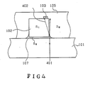
- the refractive index of fixing agent 107 is represented as n3, the following relation is desirable: n2 ⁇ n3. This is because if these relations are broken as shown in Fig.
- the material of the mold may be colored, and may contain inorganic fillers, as long as the above noted relation holds. To improve the reliability in operation of the elements, the material should preferably have a function of protecting the photoelectric converting elements.
- the above-noted problem 1 may be easily solved. That is, even if the passage of incident light is formed by a complicated structure and the cross section of the transparent substrate carrying the photoelectric converting elements is the required minimum value, stray light caused by irregular reflection of light will hardly take place and thus it is possible to avoid significant decrease in the resolution or gradient of the photoelectric converting elements.
- a solid state image pickup device which is a second embodiment of the invention and which comprises two transparent substrate chips arranged in a substantially straight line, the chips having photoelectric converting elements formed thereon.
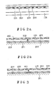
- the structure of the second embodiment of the solid state image pickup device is shown in Figs. 2a and 2b which are a schematic plan view and a schematic longitudinal cross section, respectively, of the embodiment.
- the transparent substrate chips 202 and 203 having photoelectric converting elements 205 of quartz formed thereon are fixed to a transparent support 201 of low alkali glass by means of an ultraviolet-hardened urethane-modified acrylic fixing agent 204. Further, an addition-polymerized silicone resin having a refractive index of 1.52 is used as the anti-reflection mold 105 to cover the transparent substrate chips. Further, an ultraviolet-hardened acrylic resin having a refractive index of 1.47 is charged as a filler 206 between the adjacent faces of the two transparent substrate chips and is previously hardened before being fixed to the transparent support. 108 is a dam as previously mentioned.
- the particularly important properties of the above-mentioned filler are the adhesive strength and refractive index.
- the transparent support may expand and pull the transparent substrate chips at high temperatures, causing a large tensile stress at the interface 206 between the two transparent chips. If the adhesive strength is small at the interface, then a separation will take place there at high temperatures, which separation will scatter light passing through the interface, and thus optical uniformity is broken there; for example, part of the elements can perceive "black” although the "black” should essentially be perceived as “white”. Therefore, the filler is required to have an adhesive strength which is sufficiently large to well withstand the stress.
- the optical properties of the filler are considered here.
- the filler is required to have optical properties similar to those of the transparent substrate chips mentioned in the above description of the first embodiment.
- the transparent substrate chips have a refractive index of n1 and the filler 702 has a refractive index of n3
- the following relation: n1 ⁇ n3 must hold within the ranges of wave length and temperature within which they may be used.
- refractive index n3 of the filler 702 is smaller than refractive index n1 of the transparent substrate chip, incident light 701 from a copy or the like is reflected at interface 706 of the transparent chip 703 through support member 707 and becomes reflected light 705. Then, incident light enters into not only A of the photoelectric converting elements 704, to which the light should reach, but also into B. Further, since the interface may be considered as an optically discontinuous surface between the two transparent substrate chips, n1and n3 should preferably have extremely close values and the filler should preferably have a transmission factor which is close to that of the material of the transparent substrate chips.
- the filler and the anti-reflection mold may be of the same material.
- a solid state image pickup device having two or more transparent substrate chips substantially arranged in a straight line can have the same effects as the first embodiment.
- quartz is used as the material of the transparent substrate chips 202, 203 having photoelectric converting elements 205 formed thereon, and Neoceram available from Nihon Denki Glass Corp. is used as the material of the transparent support 201.
- Neoceram available from Nihon Denki Glass Corp. is used as the material of the transparent support 201.
- an ultraviolet-hardened acrylic resin having a refractive index of 1.48 is charged as a filler 301 between the adjacent faces of the two transparent substrate chips, and a protruding portion of the filler serves, together with a sticky ultraviolet-hardened urethane-modified acrylic fixing agent 204, as an adhesive for fixation to a transparent support 201.
- the fixing agent used in this embodiment is an adhesive which has a modulus of elasticity whose value decreases as the temperature rises; the value is 2 kp/cm2(200 kPa) at room temperatures, and it decreases to one half of such value at 80°C.
- the above-mentioned problem (3) is solved by charging into the interface a filler having an adhesive strength which is large enough to withstand the tensile stress which can take place at the interface.
- the tensile stress which can take place at the interface is made as small as possible by using a fixing agent which has a modulus of elasticity whose value decreases as the temperature rises.
- the fixing agent used in accordance with the present invention preferably contains a sticky component, such as silicone, which does not contribute to the adhering function of the agent, and the adhesive components of the agent should be ones whose hardening will be accelerated by heat to an as small degree as possible.
- a sticky component such as silicone
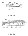
- Figs. 5a and 5b are a schematic cross sectional view and a schematic plan view of a solid state image pickup device to which the present invention is applied.
- a glass-epoxy laminated plate of 1.6 mm in thickness was used as an insulating material substrate 501, on which a conductor pattern 502 is formed and driver circuits and preamplifier circuits are provided. Further, holes 504 are provided which are sized such that they can surround a transparent substrate chip 503 which is made of quartz having a refractive index of 1.46 and on which photoelectric converting elements are formed. A photoelectric converting element 509 is formed on the transparent substrate chip 503.
- a polyester (polyethylene terephthalate) film to which a fixing agent 505 comprising a silicone adhesive is applied is used as a support 506, two transparent substrate chips and the insulating material substrate being aligned together and fixed on the sticky surface of the support.
- the transparent substrate chips and the conductor pattern on the insulating material substrate are connected by aluminum wires 507 of 35 microns in diameter, and an addition-polymerized silicone resin having a refractive index of 1.47 is applied to the surfaces and sides of the transparent substrate chips and is charged into the wiring region as an anti-reflection mold 508 which has the effects of indication and protection.
- the fourth embodiment includes measures to solve the problems (1), (2) and (3).
- the material of the insulating material substrate 501 may be either organic or inorganic, but may preferably be a BT resin-glass laminated plate such as, for example, the one available from Mitsubishi Gas Chemical Corp.. From the viewpoint of workability for boring, for example, organic substrates are preferred, while in view of heating processes such as soldering, highly heat-resistant materials such as, for example, a glass-epoxy laminated plate and a super-engeneering plastics, are preferred. A still more compact arrangement can be achieved by mounting IC's, resistors, capacitors and other circuit components on the substrate surface.
- the film used as the support 506 may be other than the previously mentioned film; for example, a polyimide tape with an adhesive available from Sumitomo Three M Corp., for example, or a polyethersulphon (PES) film having coated thereon an epoxy resin adhesive or the ultraviolet-hardened acrylic adhesive used as the fixing agent at the connection may be used as the film.
- the PSM film should preferably be used together with a fixing agent.
- a glass plate having coated thereon an adhesive as a fixing agent may be used and fixed.
- the anti-reflection mold 508 may be of a thermosetting acrylic resin having a refractive index of 1.51, an ultraviolet-hardened urethane-modified acrylic resin having a refractive index of 1.48, or a moisture-hardened silicone resin.
- a BT resin-glass laminated plate of 2.0 mm in thickness was used as the insulating material substrate, on which a conductor pattern was formed and which was bored to provide holes therethrough sized to be able to surround a transparent quartz substrate chip having photoelectric converting elements formed thereon.
- an ultraviolet-hardened acrylic adhesive was applied as an fixing agent to a support comprising a polyethersulphon (PES) film, and the insulating material substrate and the transparent substrate chips having photoelectric converting elements formed thereon were positioned relative to one another on the support film and fixed thereto.
- the pattern on the transparent substrate chips having photoelectric converting elements formed thereon was connected with the pattern on the insulating material substrate by means of aluminum wires, and a silicone gel having a shore hardness of zero was charged as an anti-reflection mold.
- the principal materials are the transparent substrate chips having photoelectric converting elements formed thereon, and the insulating material substrate.
- the quartz glass (transparent substrate chips: two chips of more than 100 mm were connected) used in the present embodiment has a coefficient of thermal expansion which is by more than two orders of magnitude different from that of the BT resin-glass laminated substrate (i.e. insulating material substrate); where the same material is used, the present embodiment is not important.
- the present embodiment when the device is operated at high temperatures of about 60°C, or when the device is left at high temperatures of about 80°C, they will exert very large forces on one another.
- the aluminum wires connecting them will undergo very large bending forces and, in the worst case, they will be broken to open.
- the properties of the organic polymer material as the anti-reflection mold, in particular the hardness reached after hardening, are found to be important.
- the hardness after hardening should be equal to or lower than shore A 20.
- the transparent substrate chips were covered on the sides and connected faces thereof by a silicone gel having a hardness of shore A 0 after hardening.
- the filler can have satisfactory reliability and performance even if it comprises a single material (silicone) instead of the materials used in the second embodiment and having a large adhesive strength.
- a polyethersulphon (PES) film coated with an epoxy resin adhesive, or a single-liquid condensed silicone of a shore hardness A 20 could be used.
- Fig. 6 shows the relation between the resistance to thermal shock (expressed by the life cycle number from -30°C to 70°C) and the shore A hardness h for different materials exemplified by a silicone resin and an urethane resin.
- the material used will not be different in coefficient of thermal expansion from one another by a degree which is more extensive than the above noted materials, but if the difference is more extensive than the above mentioned, then the hardness should further be decreased.
- the overall length is longer than the above noted (250 mm), then the hardness should also be decreased but, not so significant variations were found up to 350 mm.
- connection region If the optical properties of the connection region are the most preferential matters, then an ultraviolet hardened acrylic resin, for example, having required optical properties may be used only in the connection region.
- an ultraviolet hardened acrylic resin for example, having required optical properties may be used only in the connection region. The foregoing may be applicable to the arrangement of the first embodiment and can of course achieve similarly excellent effects.
- a silicone gel which hardens at 80°C was used as the anti-reflection mold.
- the hardening temperature of the organic polymer material is limited to a particular value, an extensive improvement in reliability can advantageously be achieved for an in-line arrangement of a plurality of transparent substrate chips having a plurality of photoelectric converting elements formed therein.
- the device can maintain excellent properties in a high-temperature shelf test at 60 - 80°C for more than 1,500 hours (here, the reliability is estimated at the maximum quality assurance condition of 80°C required for office automation devices such as usual solid state image pickup devices).
- the present embodiment may be applicable to the arrangement in which a resin is charged into the interface between the connected ends of transparent substrate chips having photoelectric converting elements formed thereon as well as to other arrangements.
- the present embodiment is particularly useful when applied to the charging arrangement.
- the present invention is characterized in that the atmosphere is heated at temperatures equal to or higher than 40°C during irradiation of ultraviolet, and that a reactive polymer material is used as the organic polymer material. It is the best to use at temperatures within the range of from 50 to 85°C.
- ultraviolet-hardened urethane-modified acrylic resins which can also be hardened by heating
- irradiation of ultraviolet in an atmosphere of temperatures equal to or higher than 40°C (50 - 80°C) followed by a heating operation at a required temperature for a required length of time will provide satisfactory hardening.
- a moisture-hardened condensed silicone is preferably hardened in an atmosphere at temperatures equal to or higher than 40°C, such as, for example, at 55°C, 90%.
- Thermally hardened materials such as, for example, a thermosetting addition-polymerized silicone resin or thermosetting acrylic resin, essentially require temperatures equal to or higher than 90°C for hardening; however, in accordance with the invention, they may also be hardened either by (1) causing a hardening process to advance, at temperatures of from 50 to 85°C at which hardening begins to take place, and for a long time (a time longer than the time which is required for hardening at temperatures equal to or higher than 90°C), or by (2) heating to a higher temperature essentially required for hardening after a temporary hardening in a similar atmosphere (50 - 85°C). Either process is applicable. Such hardening process will provide a satisfactory result for an 80°C-hardening reactive resin.
- a hardening process at temperatures equal to or higher than 40°C, particularly from 50 to 85°C may be carried out in a manner as described above in order to harden the organic polymer or the agent (particularly those designated by reference numerals 204 and 205 in Fig. 2). Then, the organic polymer is reactive, and posess an additional function of fixing the connection between the transparent substrate chips carrying the photoelectric converting elements.
Abstract
Description
- The present invention relates in general to the structure or mounting of solid state image pickup elements used for reading an image or the like, and in particular to the structure or mounting of solid state image pickup devices having a plurality of such elements arranged in a line.
- Specifically, the present invention relates to a method of mounting solid state image pickup elements formed by a transparent substrate chip having photoelectric converting elements formed therein, which is cut from a transparent substrate having photoelectric converting elements formed therein. More specifically, the present invention relates to measures to achieve improvements in accuracy and reliability of the structure of mounting of such devices, and provides an elongated solid state image pickup device.
- Prior art solid state image pickup devices of the wide area type are exemplified by the following three examples:
- Laid-open Japanese Patent Application No. 86363/1984, for example, shows a staggered arrangement of a large number of charge-coupled device (CCD) chips formed in a single crystal silicon integrated-circuit (IC), which is associated with an external electrical circuit which performs complicated operations including delaying of a signal in a manner such that the staggered arrangement appears as if it were a straight arrangement.
- Laid-open Japanese Patent Application No. 126861/1986, for example, shows an arrangement comprising a row of IC chips or the like, in which the photoelectric converting elements located at chip ends are largely different in form and structure from the other photoelectric converting elements.
- A solid state image pickup device is known, which comprises a transparent substrate, typically of a glass such as, for example, quartz glass or boro-silicate glass, having photoelectric converting elements formed thereon. Solid state image pickup devices of such type may be classified, according to the manner of incidence of light, into the following two categories:
- a) an arrangement in which
light 803 enters the device at the surface of asubstrate 801 on whichphotoelectric converting elements 802 are formed, as shown in Fig. 8; and - b) an arrangement in which
light 901 enters the device through thetransparent substrate 801, as shown in Fig. 9. - The second arrangement b) is superior in the following respects. That is, the second arrangement b) does not require so severe consideration on the optical transparency of the upper surface of the photoelectric converting elements, as compared to the first arrangement a) which requires the surface to be sealed by glass, for example, of excellent flatness. Its protective coating or protective mold may be selected from a wide variety of known coatings or molds, and a highly reliable device can be produced. The structure of the photoelectric converting element may also be selected from a wide variety of known structures.
- For these reasons, the second arrangement b) is usually employed, and it is conceivable to employ a particular arrangement shown in Fig. 10. A
transparent substrate chip 1004 with photoelectric converting elements formed thereon is fixed to atransparent support 1001 using afixing agent 1002, the photoelectric converting elements being connected to acircuit pattern 1010 on a mounting substrate by means ofwires 1003 of aluminum, gold, or the like. Incident light passes through the transparent support and the transparent substrate chip and strikes the photoelectric converting elements. Further, astructure 1006 is provided for preventing theprotective mold 1005 from flowing. The photoelectric converters and wires are potted in the protective mold, which is usually of an organic polymeric material. Driver circuits,preamplifier circuits 1007, or the like are formed on a printed circuit board and are connected by aconnector 1008. - With the prior art, however, there are the following problems.
- In the case of the prior art example 1, it is easy to arrange the chip connection associated with the in-line disposition, in which a plurality of chips are arranged in a line, since the chips are disposed in a staggered manner. Also, it is not necessary to modify the form of structure of the photoelectric converting segments in the chip ends. There is, however, a serious problem in that if it has more than two spaced rows of photoelectric converting segments, it is necessary to rearrange them into a single row. Specifically, an additional external device is required to perform complicated electrical operations including the operation of delaying a signal, and such additional device is provided within the chips, for example. In addition, since the imaging segments are spaced in the secondary scanning direction, restriction on optical elements such as lenses are large. Further, it can have little degree of freedom in the start and stop of reading and thus its application to facsimile telegraphs is limited. Thus, it has a problem in that it is generally costly and difficult to utilize.
- In the case of the prior art example 2, in which a plurality of IC chips are disposed in a line, the pitch between the photoelectric converting elements is made constant by arranging, at chip ends, photoelectric converting elements largely different in form or structure from the other photoelectric converting elements. In this example, the continuity at the chip connection ends is not complete. To ensure the continuity, special electrical processes are required.
- The arrangement of the prior art example 3 has the following problems:
- (1) Since light is introduced into the device through a transparent substrate having photoelectric converting elements formed thereon, it is expected that the passage of light will be complicated. Our experiments showed that, in accordance with the arrangement, irregular reflection is likely to occur, and stray light, for example, will degrade the resolution or gradient, limiting the reading speed. To avoid this, the following arrangement is also thinkable. That is, the
transparent substrate chip 1102 having photoelectric convertingelements 1103 formed thereon is given a structure whose cross section is shown in Fig. 11, in which
s > t* tan ϑ
where ϑ is the maximum angle of incidence of light, so that stray light fromsides 1104, such as incident rays oflight - (2) Since a transparent substrate chip having photoelectric converting elements formed thereon is fixed on a transparent support, light will pass through the transparent support and then enter the solid state image pickup device. Therefore, the support and the fixing agent must be transparent, and various requirements are imposed on their optical characteristics, such as refractive index. Particularly, in the case of an in-line arrangement of transparent substrate chips having a plurality of photoelectric converting elements formed thereon, the photoelectric converting elements are located in the close vicinity of the connection therebetween, and thus many requirements exist concerning the optical characteristics at the connection.
- (3) The transparent substrate chips having the photoelectric converting elements formed thereon and the transparent support are commonly made of different materials. For example, the transparent substrate chips having the photoelectric converting elements formed thereon are made of a highly heat-resisting quartz substrate, while the support is made of a cheap glass, such as soda glass or boro-silicate glass, since it has a wide surface area. Thus, their coefficients of thermal expansion are different by about two orders of magnitude, and, although they are important parts through which light is conducted, separation or breakage is likely to take place therebetween, and the reliability is thus very low. In view of such conditions as considered together with (2) noted above, it has been considered impossible to realize such arrangement.
- (4) It is difficult to mount the elements on the transparent support, and driver circuits, preamplifier circuits, or the like must be prepared separately.
- (5) Suitable structures for preventing the flow of the protective mold and manufacturing steps for adding such structures are necessitated.
- It is therefore an object of the invention to solve the above-mentioned problems, so as to provide a wide-area type solid state image pickup device, particularly a solid state image pickup device of the in-line type in which element chips are arranged in a line, which is equal in optical and electrical continuity to a single-line solid state image pickup device, and which is of high precision, high reliability, easy to use, of low costs, and compact in structure.
- The solid state image pickup device according to one aspect of the present invention comprises: a transparent support; one or more transparent chips mounted on the support; one or more photoelectric converting elements formed on the transparent substrate chips; a fixing agent for fixing the transparent substrate chips, at the face opposite to the face on which the photoelectric converting elements are formed, to the support at one end thereof; and an anti-reflection mold for covering the transparent substrate chips on at least the sides thereof, the refractive index of the anti-reflection mold being equal to or larger than that of the transparent substrate chips.
- In one embodiment, the transparent substrate chips are made of quartz glass, and a silicone resin having a refractive index equal to or higher than 1.465 is used as the anti-reflection mold.
- According to a second aspect of the present invention, the solid state image pickup device comprises: a transparent support; two or more transparent substrate chips mounted on the support in a manner such that a plurality of photoelectric converting elements formed on the transparent substrate chips are arranged in a straight line; a fixing agent for fixing the transparent substrate chips, at the face opposite to the face on which the photoelectric converting elements are formed, to the support at one end thereof; an anti-reflection mold for covering the transparent substrate chips on at least the sides thereof; and a filler for filling the gaps between the opposite faces of the transparent substrate chips, the anti-reflection mold and the filler having a refractive index equal to or higher than that of the transparent substrate chips.
- In an embodiment according to the second aspect of the present invention, the filler and the anti-reflection mold are of the same material.
- In another embodiment according to the second aspect of the present invention, the filler and the fixing agent are of the same material.
- According to a third aspect of the present invention, the solid state image pickup device comprises: a support which is a transparent plastic film; one or more transparent substrate chips arranged on the plastic film; one or more photoelectric converting elements formed on the transparent substrate chips; an insulating material substrate having holes bored therethrough, the holes being sized to match the transparent substrate chips; a fixing agent for fixing both of the transparent substrate chips, on the face thereof on which the photoelectric converting elements are not formed, and the insulating material substrate, on one face thereof, to the plastic film on one face thereof; and a reflecting mold for covering the transparent substrate chips on at least the sides thereof, the reflecting mold having a refractive index equal to or higher than that of the transparent substrate chips.
- In one embodiment, a conductor pattern is formed on the face of the insulating material substrate which is not in contact with the fixing agent, the photoelectric converting elements formed on the transparent substrate chips being connected with the conductor pattern.
- In another embodiment, the fixing agent has a refractive index equal to or higher than that of the transparent substrate chips.
- In a still another embodiment, the fixing agent has a modulus of elasticity which decreases as the temperature rises.
- In a further embodiment, the reflecting mold comprises one or more organic polymer materials.
- In another embodiment, the organic polymer materials have a shore hardness whose value is equal to or lower than 20 after being hardened.
- In another embodiment, the organic polymer materials are reactive polymers.
- In another embodiment, the organic polymer materials are silicone materials.
- The present invention will now be described, by way of example, with reference to the accompanying drawings, in which:
- Figs. 1a and 1b are a schematic transverse section and a plan view, respectively, of an embodiment of the solid state image pickup device according to the present invention;
- Figs. 2a and 2b are a schematic plan view and a schematic longitudinal sectional view, respectively of an embodiment of the present invention, in which two transparent substrate chips are arranged in a straight line;
- Fig. 3 is another longitudinal sectional view of an embodiment of the present invention, in which two transparent substrate chips are arranged in a straight line;
- Fig. 4 is a sectional view showing measures to prevent stray light from taking place due to the relation between refractive indices of transparent substrate chips and a fixing agent;
- Figs. 5a and 5b are a cross sectional view and an overall view, respectively, of an embodiment of the solid state image pickup device according to the present invention;
- Fig. 6 is a graph showing the reliability of organic polymer materials as a function of hardness.
- Fig. 7 is an enlarged partial longitudinal cross section of an embodiment according to the present invention, showing two transparent substrate chips arranged in a straight line, showing the junction between the two chips;
- Figs. 8 and 9 are diagrams showing two different passages in which light will enter the photoelectric converting elements;
- Fig. 10 is a cross section of a prior art solid state image pickup device; and
- Fig. 11 is a prior art technique for preventing stray light from sides of a transparent substrate chip on which photoelectric converting elements are formed;
- Figs. 1a and 1b are a schematic transverse section and a plan view, respectively, of an embodiment of the solid state image pickup device according to the present invention. A
transparent support 101 is made of barium boro-silicate glass. Atransparent substrate chip 102, which is made of quartz having a refractive index of 1.46, is fixed to one face of the support using afixing agent 107 which is an ultraviolet-hardened acrylic adhesive. The transparent substrate chip is covered on the sides and top thereof by ananti-reflection mold 105 which comprises an addition-polymerized silicone resin having a refractive index of 1.49. Thetransparent substrate chip 102 is electrically connected with aconductive pattern 110 ontransparent support 101 by analuminum wire 109. For applyinganti-reflection mold 105, adam 108, which is to be its container, is provided on the transparent support. - In the above construction, it is not always necessary to provide the anti-reflection mold. Without the anti-reflection mold, however, most of the
light rays 106 incident on thesides 104 of the transparent substrate chip will be scattered at the interface, thereby stray light is generated which will degrade the characteristics of the elements, since incident light rays are guided to the photoelectric convertingelements 103 through the transparent support and the transparent substrate. Therefore, it is desirable to cover the transparent substrate chip at least on the sides thereof. - Here, the principal requirement on the anti-reflection mold is concerned with its refractive index. Specifically, assuming that the refractive index of the transparent substrate having the photoelectric converting elements formed thereon is n₁ and the refractive index of the anti-reflection mold is n₂, there must be the following relation:
n₁≦ n₂.
Such relation must be satisfied within the used wave length range and within the used temperature range, and n₁ and n₂ preferably have as close values as possible. Further, if the refractive index of fixingagent 107 is represented as n3, the following relation is desirable: n2≧n3. This is because if these relations are broken as shown in Fig. 4, incident light 401 passing throughtransparent support 101, which should go straight intrinsically, is scattered to causestray light 402. Consequently, such light is liable to enter intophotoelektric converting element 103. The material of the mold may be colored, and may contain inorganic fillers, as long as the above noted relation holds. To improve the reliability in operation of the elements, the material should preferably have a function of protecting the photoelectric converting elements. - In accordance with this embodiment, the above-noted
problem 1 may be easily solved. That is, even if the passage of incident light is formed by a complicated structure and the cross section of the transparent substrate carrying the photoelectric converting elements is the required minimum value, stray light caused by irregular reflection of light will hardly take place and thus it is possible to avoid significant decrease in the resolution or gradient of the photoelectric converting elements. - Therefore, it is possible to achieve an improvement in the reading speed of the photoelectric converting elements.
- The arrangement of the first embodiment described above may be applied to a solid state image pickup device which is a second embodiment of the invention and which comprises two transparent substrate chips arranged in a substantially straight line, the chips having photoelectric converting elements formed thereon. The structure of the second embodiment of the solid state image pickup device is shown in Figs. 2a and 2b which are a schematic plan view and a schematic longitudinal cross section, respectively, of the embodiment.
- The
transparent substrate chips elements 205 of quartz formed thereon are fixed to atransparent support 201 of low alkali glass by means of an ultraviolet-hardened urethane-modifiedacrylic fixing agent 204. Further, an addition-polymerized silicone resin having a refractive index of 1.52 is used as theanti-reflection mold 105 to cover the transparent substrate chips. Further, an ultraviolet-hardened acrylic resin having a refractive index of 1.47 is charged as a filler 206 between the adjacent faces of the two transparent substrate chips and is previously hardened before being fixed to the transparent support. 108 is a dam as previously mentioned. - The particularly important properties of the above-mentioned filler are the adhesive strength and refractive index.
- As mentioned previously under the numerical headings (2) and (3), since in many cases the two transparent substrate chips and the transparent support are made of different materials and thus have different values of coefficient of linear expansion, the transparent support may expand and pull the transparent substrate chips at high temperatures, causing a large tensile stress at the interface 206 between the two transparent chips. If the adhesive strength is small at the interface, then a separation will take place there at high temperatures, which separation will scatter light passing through the interface, and thus optical uniformity is broken there; for example, part of the elements can perceive "black" although the "black" should essentially be perceived as "white". Therefore, the filler is required to have an adhesive strength which is sufficiently large to well withstand the stress.
- The optical properties of the filler are considered here. In some cases, since the
interface 706 between the twotransparent substrate chips 703 lies in the passage of incident light, as shown in Fig. 7, the filler is required to have optical properties similar to those of the transparent substrate chips mentioned in the above description of the first embodiment. Thus, assuming that the transparent substrate chips have a refractive index of n₁ and thefiller 702 has a refractive index of n₃, the following relation:
n₁ ≦ n₃
must hold within the ranges of wave length and temperature within which they may be used. If the refractive index n3 of thefiller 702 is smaller than refractive index n1 of the transparent substrate chip, incident light 701 from a copy or the like is reflected atinterface 706 of thetransparent chip 703 throughsupport member 707 and becomes reflected light 705. Then, incident light enters into not only A of the photoelectric convertingelements 704, to which the light should reach, but also into B. Further, since the interface may be considered as an optically discontinuous surface between the two transparent substrate chips, n₁and n₃ should preferably have extremely close values and the filler should preferably have a transmission factor which is close to that of the material of the transparent substrate chips. The filler and the anti-reflection mold may be of the same material. - In accordance with this second embodiment, a solid state image pickup device having two or more transparent substrate chips substantially arranged in a straight line can have the same effects as the first embodiment.
- In the third embodiment, quartz is used as the material of the
transparent substrate chips elements 205 formed thereon, and Neoceram available from Nihon Denki Glass Corp. is used as the material of thetransparent support 201. Also, as shown in Fig. 3, an ultraviolet-hardened acrylic resin having a refractive index of 1.48 is charged as afiller 301 between the adjacent faces of the two transparent substrate chips, and a protruding portion of the filler serves, together with a sticky ultraviolet-hardened urethane-modifiedacrylic fixing agent 204, as an adhesive for fixation to atransparent support 201. The fixing agent used in this embodiment is an adhesive which has a modulus of elasticity whose value decreases as the temperature rises; the value is 2 kp/cm²(200 kPa) at room temperatures, and it decreases to one half of such value at 80°C. - One important thing in the embodiment lies in the properties of the fixing agent for fixing the transparent substrate chips to the transparent support.
- In the foregoing second embodiment, the above-mentioned problem (3) is solved by charging into the interface a filler having an adhesive strength which is large enough to withstand the tensile stress which can take place at the interface. In the third embodiment, however, to solve the problem (3), the tensile stress which can take place at the interface is made as small as possible by using a fixing agent which has a modulus of elasticity whose value decreases as the temperature rises.
- The fixing agent used in accordance with the present invention preferably contains a sticky component, such as silicone, which does not contribute to the adhering function of the agent, and the adhesive components of the agent should be ones whose hardening will be accelerated by heat to an as small degree as possible.
- Figs. 5a and 5b are a schematic cross sectional view and a schematic plan view of a solid state image pickup device to which the present invention is applied.
- A glass-epoxy laminated plate of 1.6 mm in thickness was used as an insulating
material substrate 501, on which aconductor pattern 502 is formed and driver circuits and preamplifier circuits are provided. Further, holes 504 are provided which are sized such that they can surround atransparent substrate chip 503 which is made of quartz having a refractive index of 1.46 and on which photoelectric converting elements are formed. A photoelectric convertingelement 509 is formed on thetransparent substrate chip 503. A polyester (polyethylene terephthalate) film to which afixing agent 505 comprising a silicone adhesive is applied is used as asupport 506, two transparent substrate chips and the insulating material substrate being aligned together and fixed on the sticky surface of the support. Then, the transparent substrate chips and the conductor pattern on the insulating material substrate are connected byaluminum wires 507 of 35 microns in diameter, and an addition-polymerized silicone resin having a refractive index of 1.47 is applied to the surfaces and sides of the transparent substrate chips and is charged into the wiring region as ananti-reflection mold 508 which has the effects of indication and protection. - In accordance with the present embodiment, it is possible to solve the above-mentioned problem (4) that the previously mentioned transparent substrate chips having holes which can surround the transparent substrate chips cannot be mounted on the same substrate on which driver circuits and preamplifier circuits are provided, and moreover it is possible to solve the above-mentioned problem (5) that suitable structures for preventing the flow of the protective mold and manufacturing steps for adding such structures are necessitated. Further, since the used materials have similar properties with those used in the first, second and third embodiments, the fourth embodiment includes measures to solve the problems (1), (2) and (3).
- Now, the used materials will be described.
- The material of the insulating
material substrate 501 may be either organic or inorganic, but may preferably be a BT resin-glass laminated plate such as, for example, the one available from Mitsubishi Gas Chemical Corp.. From the viewpoint of workability for boring, for example, organic substrates are preferred, while in view of heating processes such as soldering, highly heat-resistant materials such as, for example, a glass-epoxy laminated plate and a super-engeneering plastics, are preferred. A still more compact arrangement can be achieved by mounting IC's, resistors, capacitors and other circuit components on the substrate surface. - The film used as the
support 506 may be other than the previously mentioned film; for example, a polyimide tape with an adhesive available from Sumitomo Three M Corp., for example, or a polyethersulphon (PES) film having coated thereon an epoxy resin adhesive or the ultraviolet-hardened acrylic adhesive used as the fixing agent at the connection may be used as the film. The PSM film should preferably be used together with a fixing agent. Of course, a glass plate having coated thereon an adhesive as a fixing agent may be used and fixed. - The
anti-reflection mold 508 may be of a thermosetting acrylic resin having a refractive index of 1.51, an ultraviolet-hardened urethane-modified acrylic resin having a refractive index of 1.48, or a moisture-hardened silicone resin. - In the fourth embodiment, a BT resin-glass laminated plate of 2.0 mm in thickness was used as the insulating material substrate, on which a conductor pattern was formed and which was bored to provide holes therethrough sized to be able to surround a transparent quartz substrate chip having photoelectric converting elements formed thereon. Subsequently, an ultraviolet-hardened acrylic adhesive was applied as an fixing agent to a support comprising a polyethersulphon (PES) film, and the insulating material substrate and the transparent substrate chips having photoelectric converting elements formed thereon were positioned relative to one another on the support film and fixed thereto. The pattern on the transparent substrate chips having photoelectric converting elements formed thereon was connected with the pattern on the insulating material substrate by means of aluminum wires, and a silicone gel having a shore hardness of zero was charged as an anti-reflection mold.
- As mentioned in connection with the fourth embodiment, various combinations of materials are possible in accordance with present invention. The principal materials are the transparent substrate chips having photoelectric converting elements formed thereon, and the insulating material substrate.
- The quartz glass (transparent substrate chips: two chips of more than 100 mm were connected) used in the present embodiment has a coefficient of thermal expansion which is by more than two orders of magnitude different from that of the BT resin-glass laminated substrate (i.e. insulating material substrate); where the same material is used, the present embodiment is not important. In this arrangement, therefore, when the device is operated at high temperatures of about 60°C, or when the device is left at high temperatures of about 80°C, they will exert very large forces on one another. Particularly, the aluminum wires connecting them will undergo very large bending forces and, in the worst case, they will be broken to open. To solve such problem, the properties of the organic polymer material as the anti-reflection mold, in particular the hardness reached after hardening, are found to be important. Specifically, the hardness after hardening should be equal to or lower than
shore A 20. In the present embodiment, the transparent substrate chips were covered on the sides and connected faces thereof by a silicone gel having a hardness ofshore A 0 after hardening. Here, the filler can have satisfactory reliability and performance even if it comprises a single material (silicone) instead of the materials used in the second embodiment and having a large adhesive strength. Also, a polyethersulphon (PES) film coated with an epoxy resin adhesive, or a single-liquid condensed silicone of ashore hardness A 20 could be used. - The present embodiment has achieved improvements in reliability, particularly in resistance to thermal shock, in addition to the effects as mentioned in the description of the fourth embodiment. Fig. 6 shows the relation between the resistance to thermal shock (expressed by the life cycle number from -30°C to 70°C) and the shore A hardness h for different materials exemplified by a silicone resin and an urethane resin.
- Usually, the material used will not be different in coefficient of thermal expansion from one another by a degree which is more extensive than the above noted materials, but if the difference is more extensive than the above mentioned, then the hardness should further be decreased. Of course, if the overall length is longer than the above noted (250 mm), then the hardness should also be decreased but, not so significant variations were found up to 350 mm.
- If the optical properties of the connection region are the most preferential matters, then an ultraviolet hardened acrylic resin, for example, having required optical properties may be used only in the connection region. The foregoing may be applicable to the arrangement of the first embodiment and can of course achieve similarly excellent effects.
- In a sixth embodiment, materials substantially the same as those used in the fifth embodiment were used except that a silicone gel which hardens at 80°C was used as the anti-reflection mold. In accordance with this embodiment in which the hardening temperature of the organic polymer material is limited to a particular value, an extensive improvement in reliability can advantageously be achieved for an in-line arrangement of a plurality of transparent substrate chips having a plurality of photoelectric converting elements formed therein. Specifically, it has been found that the device can maintain excellent properties in a high-temperature shelf test at 60 - 80°C for more than 1,500 hours (here, the reliability is estimated at the maximum quality assurance condition of 80°C required for office automation devices such as usual solid state image pickup devices).
- The present embodiment may be applicable to the arrangement in which a resin is charged into the interface between the connected ends of transparent substrate chips having photoelectric converting elements formed thereon as well as to other arrangements. However, it has been found that the present embodiment is particularly useful when applied to the charging arrangement. Specifically, as to the hardening, the present invention is characterized in that the atmosphere is heated at temperatures equal to or higher than 40°C during irradiation of ultraviolet, and that a reactive polymer material is used as the organic polymer material. It is the best to use at temperatures within the range of from 50 to 85°C. In the case of ultraviolet-hardened urethane-modified acrylic resins which can also be hardened by heating, it has been found that irradiation of ultraviolet in an atmosphere of temperatures equal to or higher than 40°C (50 - 80°C) followed by a heating operation at a required temperature for a required length of time will provide satisfactory hardening. A moisture-hardened condensed silicone is preferably hardened in an atmosphere at temperatures equal to or higher than 40°C, such as, for example, at 55°C, 90%. Thermally hardened materials, such as, for example, a thermosetting addition-polymerized silicone resin or thermosetting acrylic resin, essentially require temperatures equal to or higher than 90°C for hardening; however, in accordance with the invention, they may also be hardened either by (1) causing a hardening process to advance, at temperatures of from 50 to 85°C at which hardening begins to take place, and for a long time (a time longer than the time which is required for hardening at temperatures equal to or higher than 90°C), or by (2) heating to a higher temperature essentially required for hardening after a temporary hardening in a similar atmosphere (50 - 85°C). Either process is applicable. Such hardening process will provide a satisfactory result for an 80°C-hardening reactive resin.
- Even in the case of the fifth embodiment, for example, at high temperatures of from 60 to 80°C large tensile stresses will take place at the connection between the transparent substrate chips having photoelectric converting elements formed thereon. To allow the connection to withstand the stresses, (1) the hardening atmosphere is maintained at high temperatures so that the stresses appearing in the connection between the transparent substrate chips carrying the photoelectric converting elements will be compressive stresses at ordinary temperatures, and (2) an organic polymer material is used as the reactive polymer material. These measures make stable the connection between the transparent substrate chips carrying the photoelectric converting elements.
- The foregoing ideas may also be applicable to the second embodiment. That is, a hardening process at temperatures equal to or higher than 40°C, particularly from 50 to 85°C, may be carried out in a manner as described above in order to harden the organic polymer or the agent (particularly those designated by
reference numerals
Claims (13)
a transparent support; one or more transparent chips mounted on the support; one or more photoelectric converting elements formed on the transparent substrate chips; a fixing agent for fixing the transparent substrate chips, at the face opposite to the face on which the photoelectric converting elements are formed, to the support at one end thereof; and an anti-reflection mold for covering the transparent substrate chips on at least the sides thereof, the refractive index of the anti-reflection mold being equal to or larger than that of the transparent substrate chips.
a transparent support; two or more transparent substrate chips mounted on the support in a manner such that a plurality of photoelectric converting elements formed on the transparent substrate chips are arranged in a straight line; a fixing agent for fixing the transparent substrate chips, at the face opposite to the face on which the photoelectric converting elements are formed, to the support at one end thereof; an anti-reflection mold for covering the transparent substrate chips on at least the sides thereof; and a filler for filling the gaps between the opposite faces of the transparent substrate chips, the anti-reflection mold and the filler having a refractive index equal to or higher than that of the transparent substrate chips.
a support which is a transparent plastic film; one or more transparent substrate chips arranged on the plastic film; one or more photoelectric converting elements formed on the transparent substrate chips; an insulating material substrate having holes bored therethrough, the holes being sized to match the transparent substrate chips; a fixing agent for fixing both of the transparent substrate chips, on the face thereof on which the photoelectric converting elements are not formed, and the insulating material substrate, on one face thereof, to the plastic film on one face thereof; and a reflecting mold for covering the transparent substrate chips on at least the sides thereof, the reflecting mold having a refractive index equal to or higher than that of the transparent substrate chips.
Applications Claiming Priority (6)
| Application Number | Priority Date | Filing Date | Title |
|---|---|---|---|
| JP63205542A JPH0254580A (en) | 1988-08-18 | 1988-08-18 | Image sensor |
| JP205542/88 | 1988-08-18 | ||
| JP214443/88 | 1988-08-29 | ||
| JP63214452A JPH0263167A (en) | 1988-08-29 | 1988-08-29 | Image sensor |
| JP63214443A JPH0263166A (en) | 1988-08-29 | 1988-08-29 | Image sensor |
| JP214452/88 | 1988-08-29 |
Publications (3)
| Publication Number | Publication Date |
|---|---|
| EP0355522A2 true EP0355522A2 (en) | 1990-02-28 |
| EP0355522A3 EP0355522A3 (en) | 1990-08-22 |
| EP0355522B1 EP0355522B1 (en) | 1993-12-15 |
Family
ID=27328514
Family Applications (1)
| Application Number | Title | Priority Date | Filing Date |
|---|---|---|---|
| EP89114371A Expired - Lifetime EP0355522B1 (en) | 1988-08-18 | 1989-08-03 | Solid state image pickup device |
Country Status (4)
| Country | Link |
|---|---|
| US (1) | US5068713A (en) |
| EP (1) | EP0355522B1 (en) |
| DE (1) | DE68911420T2 (en) |
| HK (1) | HK106497A (en) |
Cited By (7)
| Publication number | Priority date | Publication date | Assignee | Title |
|---|---|---|---|---|
| EP0520516A1 (en) * | 1991-06-27 | 1992-12-30 | Nec Corporation | Linear image sensor |
| EP0769817A2 (en) * | 1995-10-20 | 1997-04-23 | Canon Kabushiki Kaisha | Method of fixing photoelectric semiconductor devices on a base |
| FR2748123A1 (en) * | 1996-04-27 | 1997-10-31 | Bosch Gmbh Robert | OPTICAL ASSEMBLY FOR COUPLING A LIGHT GUIDE AND PROCESS FOR ITS MANUFACTURING |
| WO1999048155A1 (en) * | 1998-03-19 | 1999-09-23 | Dr. Johannes Heidenhain Gmbh | Optoelectronic component arrangement with transparent filler material and a transparent carrier substrate |
| FR2783094A1 (en) * | 1998-09-08 | 2000-03-10 | Fujitsu Ltd | Optical semiconductor module, useful for multimedia optical networks, comprises a resin gel covering an optical semiconductor element and filling the light transmission space between the element and an optical element |
| WO2000041281A1 (en) * | 1998-12-30 | 2000-07-13 | Honeywell Inc. | Method and apparatus for hermetically sealing photonic devices |
| US6792178B1 (en) | 2000-01-12 | 2004-09-14 | Finisar Corporation | Fiber optic header with integrated power monitor |
Families Citing this family (28)
| Publication number | Priority date | Publication date | Assignee | Title |
|---|---|---|---|---|
| US5434524A (en) * | 1992-09-16 | 1995-07-18 | International Business Machines Corporation | Method of clocking integrated circuit chips |
| JP3081122B2 (en) * | 1994-07-18 | 2000-08-28 | シャープ株式会社 | Jig for transporting substrate and method of manufacturing liquid crystal display element using the same |
| US5962810A (en) * | 1997-09-09 | 1999-10-05 | Amkor Technology, Inc. | Integrated circuit package employing a transparent encapsulant |
| JPH1197656A (en) * | 1997-09-22 | 1999-04-09 | Fuji Electric Co Ltd | Semiconductor photosensor device |
| JP3400340B2 (en) * | 1998-02-20 | 2003-04-28 | 株式会社新川 | Flip chip bonding method and apparatus |
| US6483101B1 (en) * | 1999-12-08 | 2002-11-19 | Amkor Technology, Inc. | Molded image sensor package having lens holder |
| US6483030B1 (en) * | 1999-12-08 | 2002-11-19 | Amkor Technology, Inc. | Snap lid image sensor package |
| US6518659B1 (en) | 2000-05-08 | 2003-02-11 | Amkor Technology, Inc. | Stackable package having a cavity and a lid for an electronic device |
| US6424031B1 (en) | 2000-05-08 | 2002-07-23 | Amkor Technology, Inc. | Stackable package with heat sink |
| US6667544B1 (en) | 2000-06-30 | 2003-12-23 | Amkor Technology, Inc. | Stackable package having clips for fastening package and tool for opening clips |
| US7059040B1 (en) | 2001-01-16 | 2006-06-13 | Amkor Technology, Inc. | Optical module with lens integral holder fabrication method |
| KR100401020B1 (en) | 2001-03-09 | 2003-10-08 | 앰코 테크놀로지 코리아 주식회사 | Stacking structure of semiconductor chip and semiconductor package using it |
| US6906403B2 (en) * | 2002-06-04 | 2005-06-14 | Micron Technology, Inc. | Sealed electronic device packages with transparent coverings |
| US7146106B2 (en) * | 2002-08-23 | 2006-12-05 | Amkor Technology, Inc. | Optic semiconductor module and manufacturing method |
| ITMI20022467A1 (en) * | 2002-11-20 | 2004-05-21 | St Microelectronics Srl | PROCESS FOR REALIZING A BYTE SELECTION TRANSISTOR FOR |
| JP4203374B2 (en) * | 2003-08-06 | 2008-12-24 | 豊田合成株式会社 | Light emitting device |
| US6977431B1 (en) | 2003-11-05 | 2005-12-20 | Amkor Technology, Inc. | Stackable semiconductor package and manufacturing method thereof |
| US20060261458A1 (en) * | 2003-11-12 | 2006-11-23 | Amkor Technology, Inc. | Semiconductor package and manufacturing method thereof |
| US7359579B1 (en) | 2004-10-08 | 2008-04-15 | Amkor Technology, Inc. | Image sensor package and its manufacturing method |
| US20070210246A1 (en) * | 2005-04-14 | 2007-09-13 | Amkor Technology, Inc. | Stacked image sensor optical module and fabrication method |
| US7227236B1 (en) | 2005-04-26 | 2007-06-05 | Amkor Technology, Inc. | Image sensor package and its manufacturing method |
| US20070272827A1 (en) * | 2005-04-27 | 2007-11-29 | Amkor Technology, Inc. | Image sensor package having mount holder attached to image sensor die |
| US7576401B1 (en) | 2005-07-07 | 2009-08-18 | Amkor Technology, Inc. | Direct glass attached on die optical module |
| US20080237824A1 (en) * | 2006-02-17 | 2008-10-02 | Amkor Technology, Inc. | Stacked electronic component package having single-sided film spacer |
| US7675180B1 (en) | 2006-02-17 | 2010-03-09 | Amkor Technology, Inc. | Stacked electronic component package having film-on-wire spacer |
| US7633144B1 (en) | 2006-05-24 | 2009-12-15 | Amkor Technology, Inc. | Semiconductor package |
| CN101499446B (en) * | 2009-02-26 | 2013-10-16 | 光宝电子(广州)有限公司 | Wire frame tablet, packaging structure and LED packaging structure |
| DE102009042479A1 (en) * | 2009-09-24 | 2011-03-31 | Msg Lithoglas Ag | Method for producing an arrangement having a component on a carrier substrate and arrangement, and method for producing a semifinished product and semifinished product |
Citations (3)
| Publication number | Priority date | Publication date | Assignee | Title |
|---|---|---|---|---|
| JPS57164585A (en) * | 1981-04-02 | 1982-10-09 | Toshiba Corp | Photosemiconductor device |
| JPS6132469A (en) * | 1984-07-24 | 1986-02-15 | Toppan Printing Co Ltd | Color solid-state image pickup element |
| JPS61126861A (en) * | 1984-11-22 | 1986-06-14 | Toshiba Corp | Contact type image sensor |
Family Cites Families (10)
| Publication number | Priority date | Publication date | Assignee | Title |
|---|---|---|---|---|
| JPS57190455A (en) * | 1981-05-19 | 1982-11-24 | Nippon Telegr & Teleph Corp <Ntt> | Adhesion type image sensor |
| JPS5986363A (en) * | 1982-11-09 | 1984-05-18 | Toshiba Corp | Lens adjusting device of close-contact sensor |
| JPS59167037A (en) * | 1983-03-14 | 1984-09-20 | Oki Electric Ind Co Ltd | Semiconductor device |
| JPS6062278A (en) * | 1983-09-14 | 1985-04-10 | Toshiba Corp | Image sensor |
| JPS60123059A (en) * | 1983-12-08 | 1985-07-01 | Toshiba Corp | Adhesion type color image sensor |
| JPS61135280A (en) * | 1984-12-06 | 1986-06-23 | Toshiba Corp | 3-dimensional image pickup element |
| JPS61234161A (en) * | 1985-04-10 | 1986-10-18 | Matsushita Electric Ind Co Ltd | Contact type image sensor |
| JPS62104044A (en) * | 1985-10-30 | 1987-05-14 | Nec Corp | Passivating method |
| JPS62241358A (en) * | 1986-04-14 | 1987-10-22 | Hitachi Ltd | One-time program type semiconductor device |
| US4877306A (en) * | 1987-09-30 | 1989-10-31 | Corning Glass Works | Coated optical waveguide fibers |
-
1989
- 1989-08-03 EP EP89114371A patent/EP0355522B1/en not_active Expired - Lifetime
- 1989-08-03 DE DE89114371T patent/DE68911420T2/en not_active Expired - Lifetime
- 1989-08-15 US US07/393,729 patent/US5068713A/en not_active Expired - Lifetime
-
1997
- 1997-06-26 HK HK106497A patent/HK106497A/en not_active IP Right Cessation
Patent Citations (3)
| Publication number | Priority date | Publication date | Assignee | Title |
|---|---|---|---|---|
| JPS57164585A (en) * | 1981-04-02 | 1982-10-09 | Toshiba Corp | Photosemiconductor device |
| JPS6132469A (en) * | 1984-07-24 | 1986-02-15 | Toppan Printing Co Ltd | Color solid-state image pickup element |
| JPS61126861A (en) * | 1984-11-22 | 1986-06-14 | Toshiba Corp | Contact type image sensor |
Non-Patent Citations (5)
| Title |
|---|
| CONFERENCE RECORD OF THE 19TH IEEE PHOTOVOLTAIC SPECIALISTS CONFERENCE, New Orleans, 4-8 May 1987, pages 485-488, New York, US; C.A. KITCHEN et al.: "CMZ - A new generation of solar cell coverglass". * |
| PATENT ABSTRACTS OF JAPAN, vol. 10, no. 184 (E-415)(2240) 27 June 1986; & JP-A-61 032 469 (TOPPAN PRINTING) 15-02-1986 * |
| PATENT ABSTRACTS OF JAPAN, vol. 10, no. 317 (E-449)(2373) 28 October 1986; & JP-A-61 126 861 (TOSHIBA) 14-06-1986 * |
| PATENT ABSTRACTS OF JAPAN, vol. 7, no. 4 (E-151)(1149) 8 January 1983; & JP-A-57 164 585 (TOSHIBA) 09-10-1982 * |
| PATENT ABSTRACTS OF JAPAN, vol.10, no. 184 (E-415)(2240), 27 June 1986;& JP-A-61032469 * |
Cited By (13)
| Publication number | Priority date | Publication date | Assignee | Title |
|---|---|---|---|---|
| EP0520516A1 (en) * | 1991-06-27 | 1992-12-30 | Nec Corporation | Linear image sensor |
| EP1513201A2 (en) | 1995-10-20 | 2005-03-09 | Canon Kabushiki Kaisha | Photoelectric conversion apparatus and method of manufacturing the same |
| EP0769817A2 (en) * | 1995-10-20 | 1997-04-23 | Canon Kabushiki Kaisha | Method of fixing photoelectric semiconductor devices on a base |
| EP0769817A3 (en) * | 1995-10-20 | 1998-04-01 | Canon Kabushiki Kaisha | Method of fixing photoelectric semiconductor devices on a base |
| US5856699A (en) * | 1995-10-20 | 1999-01-05 | Canon Kabushiki Kaisha | Photoelectric conversion apparatus with level photoreceiving surface |
| EP1513201A3 (en) * | 1995-10-20 | 2007-03-14 | Canon Kabushiki Kaisha | Photoelectric conversion apparatus and method of manufacturing the same |
| US6352875B1 (en) | 1995-10-20 | 2002-03-05 | Canon Kabushiki Kaisha | Photoelectric conversion apparatus and method of manufacturing the same |
| FR2748123A1 (en) * | 1996-04-27 | 1997-10-31 | Bosch Gmbh Robert | OPTICAL ASSEMBLY FOR COUPLING A LIGHT GUIDE AND PROCESS FOR ITS MANUFACTURING |
| WO1999048155A1 (en) * | 1998-03-19 | 1999-09-23 | Dr. Johannes Heidenhain Gmbh | Optoelectronic component arrangement with transparent filler material and a transparent carrier substrate |
| FR2783094A1 (en) * | 1998-09-08 | 2000-03-10 | Fujitsu Ltd | Optical semiconductor module, useful for multimedia optical networks, comprises a resin gel covering an optical semiconductor element and filling the light transmission space between the element and an optical element |
| US6588949B1 (en) | 1998-12-30 | 2003-07-08 | Honeywell Inc. | Method and apparatus for hermetically sealing photonic devices |
| WO2000041281A1 (en) * | 1998-12-30 | 2000-07-13 | Honeywell Inc. | Method and apparatus for hermetically sealing photonic devices |
| US6792178B1 (en) | 2000-01-12 | 2004-09-14 | Finisar Corporation | Fiber optic header with integrated power monitor |
Also Published As
| Publication number | Publication date |
|---|---|
| US5068713A (en) | 1991-11-26 |
| EP0355522A3 (en) | 1990-08-22 |
| HK106497A (en) | 1997-08-22 |
| EP0355522B1 (en) | 1993-12-15 |
| DE68911420T2 (en) | 1994-05-11 |
| DE68911420D1 (en) | 1994-01-27 |
Similar Documents
| Publication | Publication Date | Title |
|---|---|---|
| EP0355522B1 (en) | Solid state image pickup device | |
| CN100438023C (en) | Imaging module and method for forming the same | |
| US4732446A (en) | Electrical circuit and optical data buss | |
| CN101048039B (en) | Optical/electrical circuit interconnect board and evaluation method thereof | |
| KR100839145B1 (en) | Solid-state imaging apparatus and manufacturing method thereof | |
| EP0425776A1 (en) | Package for a solid-state imaging device | |
| CN1779970A (en) | Optical rotation system for optoelectronic module | |
| JP2000098188A (en) | Optical module | |
| US6049094A (en) | Low stress package assembly for silicon-backed light valves | |
| JP2003282935A (en) | Optically coupled device and method of manufacturing the same, and electronic apparatus | |
| US7146065B2 (en) | Optical wiring board, optical bus system, and method of manufacturing optical wiring board | |
| US6907178B2 (en) | Optoelectronic assembly with embedded optical and electrical components | |
| KR100866430B1 (en) | Optoelectronic module, and method for the production thereof | |
| EP0178579B1 (en) | Mechanical part mounting chassis | |
| KR0137190B1 (en) | A direct-contact type image sensor device and an image sensor unit | |
| US20220268998A1 (en) | Optical circuit board and electronic component mounting structure using same | |
| US6788859B1 (en) | Laminate substrate containing fiber optic cables | |
| JP2000147328A (en) | Optical module and packaging method for the optical module | |
| CN217546396U (en) | Photoelectric hybrid circuit board and electronic device | |
| JP2000164803A (en) | Semiconductor device and its manufacture | |
| US7043107B2 (en) | Flexible optical connecting part | |
| JPH0846224A (en) | Optoelectric assembly,its preparation and its application | |
| US20230375780A1 (en) | Method for manufacturing photoelectric composite circuit board | |
| US7339201B2 (en) | Light emitting diode and process for producing the same | |
| JPH04113675A (en) | Semiconductor device |
Legal Events
| Date | Code | Title | Description |
|---|---|---|---|
| PUAI | Public reference made under article 153(3) epc to a published international application that has entered the european phase |
Free format text: ORIGINAL CODE: 0009012 |
|
| AK | Designated contracting states |
Kind code of ref document: A2 Designated state(s): DE FR GB NL |
|
| PUAL | Search report despatched |
Free format text: ORIGINAL CODE: 0009013 |
|
| AK | Designated contracting states |
Kind code of ref document: A3 Designated state(s): DE FR GB NL |
|
| 17P | Request for examination filed |
Effective date: 19901016 |
|
| 17Q | First examination report despatched |
Effective date: 19930208 |
|
| GRAA | (expected) grant |
Free format text: ORIGINAL CODE: 0009210 |
|
| AK | Designated contracting states |
Kind code of ref document: B1 Designated state(s): DE FR GB NL |
|
| REF | Corresponds to: |
Ref document number: 68911420 Country of ref document: DE Date of ref document: 19940127 |
|
| ET | Fr: translation filed | ||
| PLBE | No opposition filed within time limit |
Free format text: ORIGINAL CODE: 0009261 |
|
| STAA | Information on the status of an ep patent application or granted ep patent |
Free format text: STATUS: NO OPPOSITION FILED WITHIN TIME LIMIT |
|
| 26N | No opposition filed | ||
| PGFP | Annual fee paid to national office [announced via postgrant information from national office to epo] |
Ref country code: GB Payment date: 19970725 Year of fee payment: 9 |
|
| PGFP | Annual fee paid to national office [announced via postgrant information from national office to epo] |
Ref country code: FR Payment date: 19970811 Year of fee payment: 9 Ref country code: DE Payment date: 19970811 Year of fee payment: 9 |
|
| PGFP | Annual fee paid to national office [announced via postgrant information from national office to epo] |
Ref country code: NL Payment date: 19970826 Year of fee payment: 9 |
|
| PG25 | Lapsed in a contracting state [announced via postgrant information from national office to epo] |
Ref country code: GB Free format text: LAPSE BECAUSE OF NON-PAYMENT OF DUE FEES Effective date: 19980803 |
|
| PG25 | Lapsed in a contracting state [announced via postgrant information from national office to epo] |
Ref country code: NL Free format text: LAPSE BECAUSE OF NON-PAYMENT OF DUE FEES Effective date: 19990301 |
|
| GBPC | Gb: european patent ceased through non-payment of renewal fee |
Effective date: 19980803 |
|
| PG25 | Lapsed in a contracting state [announced via postgrant information from national office to epo] |
Ref country code: FR Free format text: LAPSE BECAUSE OF NON-PAYMENT OF DUE FEES Effective date: 19990430 |
|
| NLV4 | Nl: lapsed or anulled due to non-payment of the annual fee |
Effective date: 19990301 |
|
| PG25 | Lapsed in a contracting state [announced via postgrant information from national office to epo] |
Ref country code: DE Free format text: LAPSE BECAUSE OF NON-PAYMENT OF DUE FEES Effective date: 19990601 |
|
| REG | Reference to a national code |
Ref country code: FR Ref legal event code: ST |