EP0353054A2 - Quantum well structure and semiconductor device using the same - Google Patents
Quantum well structure and semiconductor device using the same Download PDFInfo
- Publication number
- EP0353054A2 EP0353054A2 EP89307615A EP89307615A EP0353054A2 EP 0353054 A2 EP0353054 A2 EP 0353054A2 EP 89307615 A EP89307615 A EP 89307615A EP 89307615 A EP89307615 A EP 89307615A EP 0353054 A2 EP0353054 A2 EP 0353054A2
- Authority
- EP
- European Patent Office
- Prior art keywords
- quantum well
- well layer
- layer
- layers
- energy
- Prior art date
- Legal status (The legal status is an assumption and is not a legal conclusion. Google has not performed a legal analysis and makes no representation as to the accuracy of the status listed.)
- Granted
Links
Images


Classifications
-
- H—ELECTRICITY
- H01—ELECTRIC ELEMENTS
- H01S—DEVICES USING THE PROCESS OF LIGHT AMPLIFICATION BY STIMULATED EMISSION OF RADIATION [LASER] TO AMPLIFY OR GENERATE LIGHT; DEVICES USING STIMULATED EMISSION OF ELECTROMAGNETIC RADIATION IN WAVE RANGES OTHER THAN OPTICAL
- H01S5/00—Semiconductor lasers
- H01S5/30—Structure or shape of the active region; Materials used for the active region
- H01S5/34—Structure or shape of the active region; Materials used for the active region comprising quantum well or superlattice structures, e.g. single quantum well [SQW] lasers, multiple quantum well [MQW] lasers or graded index separate confinement heterostructure [GRINSCH] lasers
-
- B—PERFORMING OPERATIONS; TRANSPORTING
- B82—NANOTECHNOLOGY
- B82Y—SPECIFIC USES OR APPLICATIONS OF NANOSTRUCTURES; MEASUREMENT OR ANALYSIS OF NANOSTRUCTURES; MANUFACTURE OR TREATMENT OF NANOSTRUCTURES
- B82Y20/00—Nanooptics, e.g. quantum optics or photonic crystals
-
- H—ELECTRICITY
- H01—ELECTRIC ELEMENTS
- H01L—SEMICONDUCTOR DEVICES NOT COVERED BY CLASS H10
- H01L33/00—Semiconductor devices with at least one potential-jump barrier or surface barrier specially adapted for light emission; Processes or apparatus specially adapted for the manufacture or treatment thereof or of parts thereof; Details thereof
- H01L33/02—Semiconductor devices with at least one potential-jump barrier or surface barrier specially adapted for light emission; Processes or apparatus specially adapted for the manufacture or treatment thereof or of parts thereof; Details thereof characterised by the semiconductor bodies
- H01L33/04—Semiconductor devices with at least one potential-jump barrier or surface barrier specially adapted for light emission; Processes or apparatus specially adapted for the manufacture or treatment thereof or of parts thereof; Details thereof characterised by the semiconductor bodies with a quantum effect structure or superlattice, e.g. tunnel junction
- H01L33/06—Semiconductor devices with at least one potential-jump barrier or surface barrier specially adapted for light emission; Processes or apparatus specially adapted for the manufacture or treatment thereof or of parts thereof; Details thereof characterised by the semiconductor bodies with a quantum effect structure or superlattice, e.g. tunnel junction within the light emitting region, e.g. quantum confinement structure or tunnel barrier
-
- H—ELECTRICITY
- H01—ELECTRIC ELEMENTS
- H01L—SEMICONDUCTOR DEVICES NOT COVERED BY CLASS H10
- H01L33/00—Semiconductor devices with at least one potential-jump barrier or surface barrier specially adapted for light emission; Processes or apparatus specially adapted for the manufacture or treatment thereof or of parts thereof; Details thereof
- H01L33/02—Semiconductor devices with at least one potential-jump barrier or surface barrier specially adapted for light emission; Processes or apparatus specially adapted for the manufacture or treatment thereof or of parts thereof; Details thereof characterised by the semiconductor bodies
- H01L33/26—Materials of the light emitting region
Definitions
- the present invention relates to a quantum well structure composed of a quantum well layer and a carrier confinement layer of an energy gap greater than that of the former, and a semiconductor device employing such a quantum well structure.
- a physical phenomenon such as light emission or absorption by substances (materials), or a tunneling transport of electrons in electron devices, has recently come into wide use in semiconductor devices employing the quantum well structure in the field of electronics and is now a driving force in opening up new key industries.
- a physical phenomenon largely depends on the energy gap intrinsic to the material used and, hence, is accordingly limited in its application.
- Conventional light emitting devices utilize, for emitting light, photons of an energy corresponding to the energy gap of the light emitting layer as mentioned above, and consequently, in case of changing the wavelength of light, they are subject to severe limitations in terms of materials used. This presents a serious problem in that the implementation of a blue light emitting device and an intermediate infrared light emitting device, in particular, is difficult.
- a feature of the present invention resides in a quantum well structure, which comprises a quantum well layer of thickness substantially equal to the de Broglie wavelength of electrons and carrier confinement layers of an energy gap greater than that of the quantum well layer, and in which a second material of a lattice constant different from that of a first material primarily for the quantum well layer is disposed in the quantum well layer to provide a phase shift in the period of the crystal lattice of the first material, thereby forming energy levels in the forbidden band of the quantum well layer.
- Another feature of the present invention lies in a semiconductor device which employs such a quantum well structure and is so constructed as to utilize its physical phenomenon which is caused by the energy levels in the forbidden band.
- the present invention has the feature of enabling ease in the fabrication of, for example, an intermediate infrared or blue light emitting device.
- Fig. 1 schematically illustrates a semiconductor laser of the AlGaAs series which is a typical example of a conventional light emitting device.
- the illustrated semiconductor laser has a buried stripe structure in which an n-type AlGaAs clading layer 2, a GaAs light emitting layer 3, a p-type AlGaAs clading layer 4, and a p-type GaAs layer 5 for contacting with an electrode are laminated on an n-type GaAs substrate 1 and are buried in a semi-insulating AlGaAs layer 6 for lateral mode control and for a current flow limitation.
- the lattice constant of the AlGaAs layer 2 is substantially equal to the lattice constant of the GaAs substrate 1.
- a current injection into the GaAs light emitting layer 3 across electrodes 101 and 102 a light emission or laser oscillation is obtained at a wavelength of around 0.88 ⁇ m corresponding to the energy gap of GaAs.
- Fig. 2 is a schematic diagram of the energy band for explaining the principle of emission of light in such a conventional light emitting device.
- the recombination of electrons 201 and holes 202 injected across the electrodes 101 and 102 light corresponding to the energy gap Eg of the light emitting layer is emitted as emitted photons 301.
- the semiconductor material used For example, in case of emitting light in a band between 1.3 and 1.55 ⁇ m, it is necessary to laminate InGaAs material layers on an InP substrate, and for emitting light in the range of 2 to 4 ⁇ m, InAs, GaSb, or PbS material layers must be laminated on the InP substrate. Further, it is necessary to employ, as a blue light emitting material, a material of ZnSe or ZnS, or the chalcopyrite series, such as Cu(GaAl)(SSe)2, but no excellent pn junctions are obtainable with such materials.
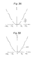
- Fig. 3 show k-space energy diagrams of electrons in a material.
- Fig. 3A is an energy diagram in a homogeneous material as in the case of the light emitting layer of the conventional light emitting device.
- atoms are regularly arranged in a period L as indicated by periodic lattice points 103 in Fig. 4A.
- the energy E of an electron increases substantially in proportion to the square of k , but the energy value undergoes discontinuous changes at points where the value of k is an integral multiple of ⁇ /L as shown in Fig. 3A. The reason for this is as follows.
- the wave function of the electron creates a standing wave by a rightward travelling wave and a leftward travelling wave and the square of the absolute value of the wave function corresponding to the probability of presence of the electron is split into two indicated by 204 and 205 in Fig. 4A.
- the energy of an electron is small in the case of presence around an atom but large away from it, the energy values of the electrons corresponding to the wave function thereof greatly differ in the cases of such squares of the absolute value of the wave function as indicated by 204 and 205, and this difference appears as an energy gap Eg.
- the value of the energy gap Eg depends on the semiconductor material used, and consequently, in the case of changing the energy gap Eg, it is necessary to use a different semiconductor material.
- the present inventors considered a structure in which the period of the crystal lattice is phase-shifted as depicted in Figs. 4B to 4D, in which the crystal lattice points 103 are phase-shifted by just one half (0.5 L) the period L.
- the square 204 of the absolute value of the wave function is minimum at the lattice points 103 on the left-hand side of the phase shift point but maximum at the lattice points 103 on the right-hand side.
- the square 205 of the absolute value of the wave function is maximum at the lattice points 103 on the left-hand side of the phase shift point but minimum on the right-hand side.
- a phase shift is provided in the crystal lattice to form energy levels in the forbidden band so that the levels are used to perform an electron transition for emission and absorption of light.
- Fig. 5A is a schematic diagram showing of an embodiment of a light emitting device which employs the quantum well structure according to the present invention.
- the light emitting region is formed by a quantum well structure which is composed of a quantum well layer (3, 9) of a thickness substantially equal to the de Broglie wavelength of electrons and carrier confinement layers (2 and 4) of an energy gap greater than that of the quantum well layer (3, 9), and in that the quantum well layer (3, 9) is made up of light emitting layers 3 formed of a main first material GaAs and a layer 9 formed of a second material of AlInSb which is different in lattice constant from GaAs.
- n-type AlGaAs layer 7 and a p-type AlGaAs layer 8 are light confining layers, in each of which the composition ratio of Al to GaAs is higher than in the carrier confining AlGaAs layers 2 and 4 to provide a lower refractive index.
- Fig. 6 is a schematic diagram of the forbidden band of the quantum well structure according to the present invention.
- Quantum well levels of electrons and holes in such light emitting layer 3 formed of the principal first material GaAs are formed as indicated by 208 and 209, and electrons 201 and holes 202 are injected into regions in the vicinities of the quantum well levels as shown in Fig. 6.
- the layer 9 formed of the second material AlInSb sandwiched between the light emitting layers 3 of the quantum well layer (3, 9) has about the same energy gap as that of the GaAs light emitting layer 3 but has a lattice constant of about 6.2 ⁇ which differs largely from the lattice constant, 5.64 ⁇ , of the GaAs light emitting layer 3.
- the AlInSb layer 9 By forming the AlInSb layer 9 to a thickness of 31 ⁇ corresponding to five cycles of its lattice constant, a phase shift corresponding to one-half the lattice constant is provided between the two GaAs light emitting layers 3 opposed across the AlInSb layer 9. Consequently, the energy levels 203 are formed in the forbidden band substantially centrally thereof as referred to previously in connection with the principle of the present invention. It is also possible to use, as the second material for the layer 9, CdTe which is nearly equal in energy gap to but largely different in lattice constant from the GaAs. In this case, the layer 9 is formed to have a thickness of about 22 ⁇ because the lattice constant of the CdTe is about 6.5 ⁇ .
- the transition of electrons across the energy levels 203 in the forbidden band, i.e. the recombination of electrons and holes occurs, by which light of an energy half that between the quantum well levels of the electrons and holes is emitted as emitted photons 302. That is to say, the energy gap Eg of the GaAs is about 1.4 eV, and assuming that the energy between the quantum well levels is around 1.6 eV, then photons of a 0.8 eV energy will be emitted.
- the light emitting device of the present invention can emit light of an energy which differs largely from the energy gap Eg determined in dependence on the semiconductor material used.
- Figs. 7A and 7B illustrate another embodiment of the present invention, which uses the same series of semiconductor materials as in Embodiment 1.
- Embodiment 1 has one quantum well layer, but this embodiment has three quantum well layers and hence employs what is called a multiple quantum well structure.
- This embodiment is exactly identical in the principle of emission of light and in operation with that previously described but affords reduction of the oscillation threshold value of the laser in accordance with the increased number of quantum well layers.
- Figs. 8A and 8B illustrate a further embodiment of the present invention, which uses a different series of semiconductor materials.
- an n-type InP substrate 11 there are laminated an n-type InP clading layer 17 for light confinement, an n-type InGaAsP layer 12 for carrier confinement, a quantum well layer composed of InGaAsP light emitting layers 13 and an AlInSb layer 19, a p-type InGaAsP layer 14 for carrier confinement, a p-type InP clading layer 18 for light confinement, and a p-type InGaAsP layer 15 for contacting with an electrode, these layers being buried in mesa-stripe form in a semi-insulating InP layer 16.
- the InGaAsP layers (12, 13, 14 and 15) are all lattice-matched with the n-type InP substrate 11.
- the light emitting region has a quantum well structure comprising a quantum well layer (13, 19) of a thickness nearly equal to the de Broglie wavelength and the carrier confining layers (12, 14) having an energy gap greater than that of the quantum well layer.
- the quantum well layer is composed of the layers 13 formed of InGaAsP which is primarily a first material and the layer 19 formed of a second material AlInSb which has a lattice constant different from that of the InGaAsP.
- Fig. 8B there is shown, on an enlarged scale, the quantum well layer (13, 19) portion indicated by hatching.
- the AlInSb layer 19 of the second material, interposed between the two InGaAsP light emitting layers 13 of the quantum well layer, has about the same energy gap as that of each light emitting layer 13, but its lattice constant is about 6.35 ⁇ , markedly different from the lattice constant, 5.78 ⁇ , of the light emitting layer 13.
- a phase shift corresponding to one-half the lattice is provided between the two InGaAsP light emitting layers 13 opposed across the AlInSb layer 9.
- energy levels are created in the forbidden band substantially centrally thereof as mentioned previously with respect to the principle of the invention.
- the laser of the InGaAsP/InP series emits light at a wavelength of 2.6 ⁇ m or so.
- Figs. 9A and 9B illustrate yet another embodiment of the present invention, which uses a different series of materials or the III-V group materials and the II-VI group or chalcopyrite series materials and emits light through optical pumping.
- a light confining clading layer 26 formed of Cu(GaAl)(SSe)2, a carrier confining Cu(GaAl)(SSe)2 layer 22, a quantum well layer composed of light emitting Cu(GaAl)(SSe)2 layers 23 and a GaP layer 28, a carrier confining Cu(GaAl)(SSe)2 layer 24, and a light confining Cu(GaAl)(SSe)2 clad layer 27, which are the chalcopyrite series material, these layers being buried in a mesa-stripe form in a semi-insulating Cu(GaAl)(SSe)2 layer 25.
- the Cu(GaAl)(SSe)2 layers are all la
- Fig. 10 is a schematic representation of the forbidden band of the quantum well structure according to the present invention.
- Quantum well levels of electrons and holes in the light emitting layers 23 formed of the Cu(GaAl)(SSe)2 which is principally a first material are formed as indicated by 210 and 211, respectively.
- the GaP layer 28 formed of a second material, interposed between the two Cu(GaAl)(SSe)2 light emitting layers 23 of the quantum well layer, has substantially the same energy gap as those of the light emitting layers 23.
- the lattice constant of the Cu(GaAl)(SSe)2 of each light emitting layer is about 5.43 ⁇ , equal to that of the GaP substrate 21, in a direction perpendicular to its thickness but 10.5 ⁇ or so, of about twice the above-mentioned lattice constant, in the direction of the layer thickness.
- energy levels 212 are established in the forbidden band substantially centrally thereof as mentioned previously in respect of the principle of the invention.
- the energy gap of the Cu(GaAl)(SSe)2 light emitting layer 23 is around 2.3 eV, and an energy of 2.8 eV is obtained as energy between the quantum well levels of electrons and holes.
- the thus excited electrons 201 and holes 202 recombine, emitting blue light having a wavelength of approximately 0.44 ⁇ m corresponding to the above-mentioned energy 2.8 eV.
- the probability of recombination of the electrons and holes across the energy levels 212 in the forbidden band is low and a direct transition between the quantum well levels is predominant.
- a laser oscillation of a blue colour can be obtained by fully vigorous optical pumping.
- the GaP layer 28 may also be replaced by a layer of ZnTe which has an energy gap similar to that of the GaP.
- the invention can easily be implemented using substrates of other materials as well.
- the first and second materials are not limited specifically to the semiconductors but may also be conductive materials and insulating materials.
- the present invention has been described as being applied to light emitting devices which are semiconductor lasers using the buried stripe structure, the invention is easily applicable as well to semiconductor lasers or light emitting diodes employing other stripe structures. It is evident from the embodiment shown in Figures 9A and 9B that the present invention can also be applied to photodetectors.
- the energy levels in the forbidden band according to the present invention can also be utilized as tunnelling levels of an electron tunnelling transport phenomenon.
- the present invention permits the materialization of quantum well structures and semiconductor devices which are free from limitations by the energy gaps inherent to the materials used.
- phase shift corresponding to one-half the crystal lattice constant of the first material it is possible to easily obtain a quantum well structure having energy levels formed in the forbidden band and a semiconductor device employing such a quantum well structure.
- the quantum well layer made up of the InGaAsP layers 3 and the AlInSb layer 9 and the carrier confining layer (2, 4) formed by the InGaAsP layer it is possible to emit photons having an energy of approximately 0.5 eV.
- the quantum well layer composed of the Cu(GaAl) (SSe)2 layers 23 and the GaP layer 28 and the carrier confining layer (22, 24) formed by the Cu(GaAl)(SSe)2 layer, it is possible to emit photons having an energy of 2.8 eV.
- the laser oscillation threshold value can be reduced through use of a multiple quantum well structure formed by laminating pluralities of quantum well layers and carrier confining layers.
- a semiconductor device can easily be produced by using semiconductors as the first and second materials.
- a semiconductor device which is not restricted by the energy gaps inherent to the materials used can be manufactured through use of the quantum well structure which utilizes a physical phenomenon caused by the energy levels in the forbidden band of the material.
- a light emitting device which is not restricted by the energy gaps inherent to the material used can be produced through utilization of the physical phenomenon that the emission of light accompanies the transition of electrons across the energy levels.
- a blue light emitting device can be produced through utilization of the physical phenomenon that the emission of light corresponding to the energy gap of the quantum well layer accompanies optical pumping across the energy levels.
- the light emitting devices of the foregoing embodiments emit light not only of a wavelength corresponding to the energy gap inherent to the material used but also of a wave-length twice or half that wavelength.
- the present invention is widely applicable to fiber optic communications and various instrumentations as well as to magneto-optical disks, compact disks, laser printers, miniature display lamps, and various other terminal equipments. Hence the present invention is of great practical utility.
Abstract
Description
- The present invention relates to a quantum well structure composed of a quantum well layer and a carrier confinement layer of an energy gap greater than that of the former, and a semiconductor device employing such a quantum well structure.
- A physical phenomenon, such as light emission or absorption by substances (materials), or a tunneling transport of electrons in electron devices, has recently come into wide use in semiconductor devices employing the quantum well structure in the field of electronics and is now a driving force in opening up new key industries. However, such a physical phenomenon largely depends on the energy gap intrinsic to the material used and, hence, is accordingly limited in its application.
- A conventional light emitting semiconductor device will now be described as a concrete example.
- Because of their excellent features such as small size, light weight, and high efficiency, light emitting semiconductor devices are now being used widely in fiber optic communications and various instrumentations as well as in magneto-optical disks, compact disks, laser printers, miniature display lamps, and various other terminal equipments. For further broading of their application it is of enormous importance to enlarge the range of emission wavelength of the light emitting semiconductor devices. There is a demand for green to blue light sources in the visible region and, in the infrared region, for light sources for analysing special gases and for fluoride fiber optic communications.
- Conventional light emitting devices utilize, for emitting light, photons of an energy corresponding to the energy gap of the light emitting layer as mentioned above, and consequently, in case of changing the wavelength of light, they are subject to severe limitations in terms of materials used. This presents a serious problem in that the implementation of a blue light emitting device and an intermediate infrared light emitting device, in particular, is difficult.
- Such a difficulty is experienced not only in light emitting devices but also in photo detectors. In the field of electronic devices many attempts are also being made for sophistication of the electron transport phenomenon by mutually combining various materials of different energy gaps, but these attempts are also limited basically by the energy gaps inherent in the materials used.
- It is an object of the present invention to provide a quantum well structure which is free from the limitations imposed by energy gaps inherent to the materials used, and a semiconductor device which employs such a quantum well structures.
- A feature of the present invention resides in a quantum well structure, which comprises a quantum well layer of thickness substantially equal to the de Broglie wavelength of electrons and carrier confinement layers of an energy gap greater than that of the quantum well layer, and in which a second material of a lattice constant different from that of a first material primarily for the quantum well layer is disposed in the quantum well layer to provide a phase shift in the period of the crystal lattice of the first material, thereby forming energy levels in the forbidden band of the quantum well layer. Another feature of the present invention lies in a semiconductor device which employs such a quantum well structure and is so constructed as to utilize its physical phenomenon which is caused by the energy levels in the forbidden band. In concrete terms, the present invention has the feature of enabling ease in the fabrication of, for example, an intermediate infrared or blue light emitting device.
- Embodiments of the present invention will now be described by way of example in comparison with prior art and with reference to the accompanying drawings, in which:
- Fig. 1 is a schematic diagram showing the construction of a conventional light emitting device;
- Fig. 2 is a diagram of an energy band structure explanatory of the principle of emission of light in the conventional light emitting device;
- Fig. 3A is a schematic k-space energy diagram of the conventional light emitting device;
- Fig. 3B is a schematic k-space energy diagram of an embodiment of a light emitting device of the present invention;
- Fig. 4A is a waveform diagram showing the relationship between crystal lattice points and a square of the absolute value of a wave function in the conventional light emitting device;
- Figs. 4B to 4D are waveform diagrams each showing the relationship between crystal lattice points and a square of the absolute value of a wave function in embodiments of the light emitting device of the present invention;
- Figs. 5A and 5B, 7A and 7B, 8A and 8B, and 9A and 9B are schematic diagrams illustrating embodiments of light emitting devices of the present invention; and
- Figs. 6 and 10 are energy band diagrams of embodiments of the light emitting device of the present invention.
- To make differences between prior art and the present invention clear, an example of prior art will first be described.
- Fig. 1 schematically illustrates a semiconductor laser of the AlGaAs series which is a typical example of a conventional light emitting device. The illustrated semiconductor laser has a buried stripe structure in which an n-type
AlGaAs clading layer 2, a GaAslight emitting layer 3, a p-typeAlGaAs clading layer 4, and a p-type GaAs layer 5 for contacting with an electrode are laminated on an n-type GaAs substrate 1 and are buried in asemi-insulating AlGaAs layer 6 for lateral mode control and for a current flow limitation. The lattice constant of theAlGaAs layer 2 is substantially equal to the lattice constant of the GaAs substrate 1. By a current injection into the GaAslight emitting layer 3 acrosselectrodes 101 and 102 a light emission or laser oscillation is obtained at a wavelength of around 0.88 µm corresponding to the energy gap of GaAs. Fig. 2 is a schematic diagram of the energy band for explaining the principle of emission of light in such a conventional light emitting device. By the recombination ofelectrons 201 andholes 202 injected across theelectrodes photons 301. - To change the wavelength of light which is emitted from the light emitting semiconductor device of such a structure, there is no choice but to change the semiconductor material used. For example, in case of emitting light in a band between 1.3 and 1.55 µm, it is necessary to laminate InGaAs material layers on an InP substrate, and for emitting light in the range of 2 to 4 µm, InAs, GaSb, or PbS material layers must be laminated on the InP substrate. Further, it is necessary to employ, as a blue light emitting material, a material of ZnSe or ZnS, or the chalcopyrite series, such as Cu(GaAl)(SSe)₂, but no excellent pn junctions are obtainable with such materials.
- With reference to the accompanying drawings, the present invention will hereinafter be described in detail in connection with a light emitting device.
- A description will be given first of the principle of the present invention. Fig. 3 show k-space energy diagrams of electrons in a material. Fig. 3A is an energy diagram in a homogeneous material as in the case of the light emitting layer of the conventional light emitting device. In the homogeneous material atoms are regularly arranged in a period L as indicated by
periodic lattice points 103 in Fig. 4A. The energy E of an electron increases substantially in proportion to the square of k, but the energy value undergoes discontinuous changes at points where the value of k is an integral multiple of ±π/L as shown in Fig. 3A. The reason for this is as follows. For example, at the point where k = ±π/L, the wave function of the electron creates a standing wave by a rightward travelling wave and a leftward travelling wave and the square of the absolute value of the wave function corresponding to the probability of presence of the electron is split into two indicated by 204 and 205 in Fig. 4A. Since the energy of an electron is small in the case of presence around an atom but large away from it, the energy values of the electrons corresponding to the wave function thereof greatly differ in the cases of such squares of the absolute value of the wave function as indicated by 204 and 205, and this difference appears as an energy gap Eg. The value of the energy gap Eg depends on the semiconductor material used, and consequently, in the case of changing the energy gap Eg, it is necessary to use a different semiconductor material. - In view of the above, the present inventors considered a structure in which the period of the crystal lattice is phase-shifted as depicted in Figs. 4B to 4D, in which the
crystal lattice points 103 are phase-shifted by just one half (0.5 L) the period L. As will be seen from Fig. 4B, thesquare 204 of the absolute value of the wave function is minimum at thelattice points 103 on the left-hand side of the phase shift point but maximum at thelattice points 103 on the right-hand side. In contrast thereto, thesquare 205 of the absolute value of the wave function is maximum at thelattice points 103 on the left-hand side of the phase shift point but minimum on the right-hand side. Consequently, electron energies for the both wave functions are equivalent to each other and the equivalent energy value is exactly one half that for the two wave functions in the case of the regular arrangement of the lattice points in Fig. 4A. As a result,energy levels 203 are created in the forbidden band as depicted in Fig. 3B. The squares of the absolute values of the actual wave functions for thelevels 203 in the forbidden band become such as indicated by 206 and 207 in Fig. 4C. While in Figs. 4B and 4C the phase shift corresponding to one-half the crystal lattice constant is provided by a spacing of 1.5 L, a similar phase shift could be also implemented by a spacing of 0.5 L as depicted in Fig. 4D, in which referencenumerals - As described above, according to the present invention, a phase shift is provided in the crystal lattice to form energy levels in the forbidden band so that the levels are used to perform an electron transition for emission and absorption of light.
- Fig. 5A is a schematic diagram showing of an embodiment of a light emitting device which employs the quantum well structure according to the present invention. This embodiment differs widely from the prior art example of Fig. 1 in that the light emitting region is formed by a quantum well structure which is composed of a quantum well layer (3, 9) of a thickness substantially equal to the de Broglie wavelength of electrons and carrier confinement layers (2 and 4) of an energy gap greater than that of the quantum well layer (3, 9), and in that the quantum well layer (3, 9) is made up of light emitting
layers 3 formed of a main first material GaAs and alayer 9 formed of a second material of AlInSb which is different in lattice constant from GaAs. In Fig. 5B there is shown, on an enlarged scale, the quantum well layer (3, 9) portion indicated by hatching. An n-type AlGaAs layer 7 and a p-type AlGaAs layer 8 are light confining layers, in each of which the composition ratio of Al to GaAs is higher than in the carrier confiningAlGaAs layers - Fig. 6 is a schematic diagram of the forbidden band of the quantum well structure according to the present invention. Quantum well levels of electrons and holes in such
light emitting layer 3 formed of the principal first material GaAs are formed as indicated by 208 and 209, andelectrons 201 andholes 202 are injected into regions in the vicinities of the quantum well levels as shown in Fig. 6. Thelayer 9 formed of the second material AlInSb sandwiched between the light emittinglayers 3 of the quantum well layer (3, 9) has about the same energy gap as that of the GaAslight emitting layer 3 but has a lattice constant of about 6.2 Å which differs largely from the lattice constant, 5.64 Å, of the GaAslight emitting layer 3. By forming theAlInSb layer 9 to a thickness of 31 Å corresponding to five cycles of its lattice constant, a phase shift corresponding to one-half the lattice constant is provided between the two GaAslight emitting layers 3 opposed across theAlInSb layer 9. Consequently, theenergy levels 203 are formed in the forbidden band substantially centrally thereof as referred to previously in connection with the principle of the present invention. It is also possible to use, as the second material for thelayer 9, CdTe which is nearly equal in energy gap to but largely different in lattice constant from the GaAs. In this case, thelayer 9 is formed to have a thickness of about 22 Å because the lattice constant of the CdTe is about 6.5 Å. In such a light emitting device the transition of electrons across theenergy levels 203 in the forbidden band, i.e. the recombination of electrons and holes occurs, by which light of an energy half that between the quantum well levels of the electrons and holes is emitted as emittedphotons 302. That is to say, the energy gap Eg of the GaAs is about 1.4 eV, and assuming that the energy between the quantum well levels is around 1.6 eV, then photons of a 0.8 eV energy will be emitted. Laser diodes of the conventional structure made of GaAs series, shown in Fig. 1, oscillates at a wavelength of 0.88 µm or so, whereas, according to the structure of the present invention, a laser using the same series of semiconductor materials oscillates at a wavelength of 1.55 µm or so. As will be appreciated from the above, the light emitting device of the present invention can emit light of an energy which differs largely from the energy gap Eg determined in dependence on the semiconductor material used. - Figs. 7A and 7B illustrate another embodiment of the present invention, which uses the same series of semiconductor materials as in Embodiment 1. Embodiment 1 has one quantum well layer, but this embodiment has three quantum well layers and hence employs what is called a multiple quantum well structure. This embodiment is exactly identical in the principle of emission of light and in operation with that previously described but affords reduction of the oscillation threshold value of the laser in accordance with the increased number of quantum well layers.
- Figs. 8A and 8B illustrate a further embodiment of the present invention, which uses a different series of semiconductor materials. On an n-type InP substrate 11 there are laminated an n-type
InP clading layer 17 for light confinement, an n-type InGaAsP layer 12 for carrier confinement, a quantum well layer composed of InGaAsPlight emitting layers 13 and anAlInSb layer 19, a p-type InGaAsP layer 14 for carrier confinement, a p-typeInP clading layer 18 for light confinement, and a p-type InGaAsP layer 15 for contacting with an electrode, these layers being buried in mesa-stripe form in asemi-insulating InP layer 16. The InGaAsP layers (12, 13, 14 and 15) are all lattice-matched with the n-type InP substrate 11. The light emitting region has a quantum well structure comprising a quantum well layer (13, 19) of a thickness nearly equal to the de Broglie wavelength and the carrier confining layers (12, 14) having an energy gap greater than that of the quantum well layer. The quantum well layer is composed of thelayers 13 formed of InGaAsP which is primarily a first material and thelayer 19 formed of a second material AlInSb which has a lattice constant different from that of the InGaAsP. In Fig. 8B, there is shown, on an enlarged scale, the quantum well layer (13, 19) portion indicated by hatching. TheAlInSb layer 19 of the second material, interposed between the two InGaAsPlight emitting layers 13 of the quantum well layer, has about the same energy gap as that of each light emittinglayer 13, but its lattice constant is about 6.35 Å, markedly different from the lattice constant, 5.78 Å, of thelight emitting layer 13. By forming theAlInSb layer 19 to a thickness of 37 Å corresponding to about six cycles of its lattice constant, a phase shift corresponding to one-half the lattice is provided between the two InGaAsPlight emitting layers 13 opposed across theAlInSb layer 9. As a result, energy levels are created in the forbidden band substantially centrally thereof as mentioned previously with respect to the principle of the invention. In such a light emitting device the transition of electrons across the energy levels in the forbidden band, i.e. the recombination of electrons and holes occurs, emitting light of an energy equal to one half the energy gap Eg. That is to say, the energy gap between the quantum well levels of the InGaAsPlight emitting layers 13 is about 0.95 eV and photons of a 0.475 eV energy, which is half the above energy gap, are emitted. In other words, the laser of the InGaAsP/InP series emits light at a wavelength of 2.6 µm or so. - Figs. 9A and 9B illustrate yet another embodiment of the present invention, which uses a different series of materials or the III-V group materials and the II-VI group or chalcopyrite series materials and emits light through optical pumping. On a
GaP substrate 21 there are laminated a light confiningclading layer 26 formed of Cu(GaAl)(SSe)₂, a carrier confining Cu(GaAl)(SSe)₂layer 22, a quantum well layer composed of light emitting Cu(GaAl)(SSe)₂layers 23 and aGaP layer 28, a carrier confining Cu(GaAl)(SSe)₂layer 24, and a light confining Cu(GaAl)(SSe)₂ cladlayer 27, which are the chalcopyrite series material, these layers being buried in a mesa-stripe form in a semi-insulating Cu(GaAl)(SSe)₂layer 25. The Cu(GaAl)(SSe)₂ layers are all lattice-matched with theGaP substrate 21. - Fig. 10 is a schematic representation of the forbidden band of the quantum well structure according to the present invention. Quantum well levels of electrons and holes in the
light emitting layers 23 formed of the Cu(GaAl)(SSe)₂ which is principally a first material are formed as indicated by 210 and 211, respectively. TheGaP layer 28 formed of a second material, interposed between the two Cu(GaAl)(SSe)₂light emitting layers 23 of the quantum well layer, has substantially the same energy gap as those of the light emitting layers 23. On the other hand, the lattice constant of the Cu(GaAl)(SSe)₂ of each light emitting layer is about 5.43 Å, equal to that of theGaP substrate 21, in a direction perpendicular to its thickness but 10.5 Å or so, of about twice the above-mentioned lattice constant, in the direction of the layer thickness. By forming theGaP layer 28 to a thickness equal to one cycle of its lattice constant, a phase shift corresponding to one-half the lattice constant is provided between the two Cu(GaAl)(SSe)₂ light emitting layers disposed on both sides of theGaP layer 28 as shown in Fig. 4D. Consequently,energy levels 212 are established in the forbidden band substantially centrally thereof as mentioned previously in respect of the principle of the invention. The energy gap of the Cu(GaAl)(SSe)₂light emitting layer 23 is around 2.3 eV, and an energy of 2.8 eV is obtained as energy between the quantum well levels of electrons and holes. By optical pumping using, asexciting photons 303, the output light of a GaAs high output semiconductor laser which has a photon energy of about 1.4 eV, the electrons and holes are excited at thequantum well levels energy levels 212 in the forbidden band. The thusexcited electrons 201 andholes 202 recombine, emitting blue light having a wavelength of approximately 0.44 µm corresponding to the above-mentioned energy 2.8 eV. In such a vigorous optical pumping, the probability of recombination of the electrons and holes across theenergy levels 212 in the forbidden band is low and a direct transition between the quantum well levels is predominant. A laser oscillation of a blue colour can be obtained by fully vigorous optical pumping. Incidentally, theGaP layer 28 may also be replaced by a layer of ZnTe which has an energy gap similar to that of the GaP. - While in the above the present invention has been described in connection with the examples employing semiconductor substrates as of GaAs, InP and GaP, the invention can easily be implemented using substrates of other materials as well. The first and second materials are not limited specifically to the semiconductors but may also be conductive materials and insulating materials. Although in the above the present invention has been described as being applied to light emitting devices which are semiconductor lasers using the buried stripe structure, the invention is easily applicable as well to semiconductor lasers or light emitting diodes employing other stripe structures. It is evident from the embodiment shown in Figures 9A and 9B that the present invention can also be applied to photodetectors. Moreover, the energy levels in the forbidden band according to the present invention can also be utilized as tunnelling levels of an electron tunnelling transport phenomenon.
- As described above in detail, the present invention permits the materialization of quantum well structures and semiconductor devices which are free from limitations by the energy gaps inherent to the materials used.
- By providing the phase shift corresponding to one-half the crystal lattice constant of the first material, it is possible to easily obtain a quantum well structure having energy levels formed in the forbidden band and a semiconductor device employing such a quantum well structure.
- With the quantum well layer made up of the InGaAsP layers 3 and the
AlInSb layer 9 and the carrier confining layer (2, 4) formed by the InGaAsP layer it is possible to emit photons having an energy of approximately 0.5 eV. - With the quantum well layer composed of the Cu(GaAl) (SSe)₂
layers 23 and theGaP layer 28 and the carrier confining layer (22, 24) formed by the Cu(GaAl)(SSe)₂ layer, it is possible to emit photons having an energy of 2.8 eV. - The laser oscillation threshold value can be reduced through use of a multiple quantum well structure formed by laminating pluralities of quantum well layers and carrier confining layers.
- A semiconductor device can easily be produced by using semiconductors as the first and second materials.
- A semiconductor device which is not restricted by the energy gaps inherent to the materials used can be manufactured through use of the quantum well structure which utilizes a physical phenomenon caused by the energy levels in the forbidden band of the material.
- A light emitting device which is not restricted by the energy gaps inherent to the material used can be produced through utilization of the physical phenomenon that the emission of light accompanies the transition of electrons across the energy levels.
- A blue light emitting device can be produced through utilization of the physical phenomenon that the emission of light corresponding to the energy gap of the quantum well layer accompanies optical pumping across the energy levels.
- The light emitting devices of the foregoing embodiments emit light not only of a wavelength corresponding to the energy gap inherent to the material used but also of a wave-length twice or half that wavelength. The present invention is widely applicable to fiber optic communications and various instrumentations as well as to magneto-optical disks, compact disks, laser printers, miniature display lamps, and various other terminal equipments. Hence the present invention is of great practical utility.
Claims (10)
characterized in that a second material (9,19,28) of a lattice constant different from that of a main first material (3,13,23) of the quantum well layer is disposed in the quantum well layer to provide a phase shift in the period of the crystal lattice of the first material, thereby forming energy levels in the forbidden band of the quantum well layer.
Applications Claiming Priority (2)
| Application Number | Priority Date | Filing Date | Title |
|---|---|---|---|
| JP63185578A JPH0236585A (en) | 1988-07-27 | 1988-07-27 | Quantum well structure and semiconductor element provided therewith |
| JP185578/88 | 1988-07-27 |
Publications (3)
| Publication Number | Publication Date |
|---|---|
| EP0353054A2 true EP0353054A2 (en) | 1990-01-31 |
| EP0353054A3 EP0353054A3 (en) | 1991-03-13 |
| EP0353054B1 EP0353054B1 (en) | 1997-01-02 |
Family
ID=16173264
Family Applications (1)
| Application Number | Title | Priority Date | Filing Date |
|---|---|---|---|
| EP89307615A Expired - Lifetime EP0353054B1 (en) | 1988-07-27 | 1989-07-27 | Quantum well structure and semiconductor device using the same |
Country Status (4)
| Country | Link |
|---|---|
| US (1) | US5122844A (en) |
| EP (1) | EP0353054B1 (en) |
| JP (1) | JPH0236585A (en) |
| DE (1) | DE68927598T2 (en) |
Cited By (2)
| Publication number | Priority date | Publication date | Assignee | Title |
|---|---|---|---|---|
| EP0457571A2 (en) * | 1990-05-17 | 1991-11-21 | Mitsubishi Denki Kabushiki Kaisha | Strained superlattice semiconductor structure |
| WO1997036335A1 (en) * | 1996-03-28 | 1997-10-02 | Philips Electronics N.V. | Radiation-emitting semiconductor diode having a separate confinement layer comprising a semiconductor material with at most 30 % aluminum or a semiconductor material free of aluminum |
Families Citing this family (13)
| Publication number | Priority date | Publication date | Assignee | Title |
|---|---|---|---|---|
| US5488234A (en) * | 1993-03-18 | 1996-01-30 | Matsushita Electric Industrial Co., Ltd. | Semiconductor element having bivalent and VI group element and an insulating layer |
| US5789772A (en) * | 1994-07-15 | 1998-08-04 | The Whitaker Corporation | Semi-insulating surface light emitting devices |
| US5552603A (en) * | 1994-09-15 | 1996-09-03 | Martin Marietta Corporation | Bias and readout for multicolor quantum well detectors |
| US5629232A (en) * | 1994-11-14 | 1997-05-13 | The Whitaker Corporation | Method of fabricating semiconductor light emitting devices |
| US5608234A (en) * | 1994-11-14 | 1997-03-04 | The Whitaker Corporation | Semi-insulating edge emitting light emitting diode |
| US5924002A (en) * | 1994-12-22 | 1999-07-13 | Sony Corporation | Method of manufacturing a semiconductor device having ohmic electrode |
| KR0166497B1 (en) * | 1995-03-24 | 1999-01-15 | 김주용 | Phase inversion mask and the method of production therefrom |
| US5977566A (en) * | 1996-06-05 | 1999-11-02 | Kabushiki Kaisha Toshiba | Compound semiconductor light emitter |
| US7140110B2 (en) * | 2003-06-04 | 2006-11-28 | Lake Ronald W | Folding knife having a locking mechanism |
| US20050097755A1 (en) * | 2003-10-31 | 2005-05-12 | Galyean Timothy J. | Folding knife having a locking mechanism |
| US20050144730A1 (en) * | 2004-01-05 | 2005-07-07 | Barber Launce R. | Combination carabiner and wrench device |
| JP2008071803A (en) * | 2006-09-12 | 2008-03-27 | Institute Of National Colleges Of Technology Japan | Compound mixed crystal semiconductor light-emitting device |
| JP6220864B2 (en) * | 2012-05-08 | 2017-10-25 | メイコム テクノロジー ソリューションズ ホールディングス インコーポレイテッド | Laser with improved beam shape |
Family Cites Families (4)
| Publication number | Priority date | Publication date | Assignee | Title |
|---|---|---|---|---|
| JPH0821708B2 (en) * | 1985-11-14 | 1996-03-04 | 株式会社豊田中央研究所 | Semiconductor element |
| US4802181A (en) * | 1986-11-27 | 1989-01-31 | Nec Corporation | Semiconductor superlattice light emitting sevice |
| US4857971A (en) * | 1987-03-23 | 1989-08-15 | Xerox Corporation | (IV)x (III-V)1-x alloys formed in situ in III-V heterostructures |
| US4862471A (en) * | 1988-04-22 | 1989-08-29 | University Of Colorado Foundation, Inc. | Semiconductor light emitting device |
-
1988
- 1988-07-27 JP JP63185578A patent/JPH0236585A/en active Pending
-
1989
- 1989-07-27 DE DE68927598T patent/DE68927598T2/en not_active Expired - Fee Related
- 1989-07-27 EP EP89307615A patent/EP0353054B1/en not_active Expired - Lifetime
-
1991
- 1991-05-22 US US07/706,542 patent/US5122844A/en not_active Expired - Lifetime
Non-Patent Citations (3)
| Title |
|---|
| APPLIED PHYSICS LETTERS, vol. 52, no. 13, 28th March 1988, pages 1080-1082, New York, US; L.A. KOLODZIEJSKI et al.: "Excitonic trapping from atomic layer epitaxial ZnTe within ZnSe/(Zn,Mn)Se heterostructures" * |
| ELECTRONIC LETTERS, vol. 18, no. 25/26, 9th December 1982, pages 1095-1097, London, GB; R.D. BURNHAM et al.: "Low-threshold single quantum well (60 A) GaAlAs lasers grown by MO-CVD with Mg AS p-type dopant" * |
| SOVIET PHYSICS SEMICONDUCTORS, vol. 22, no. 6, June 1988, pages 650-652, New York, US; Z.I. ALFEROV et al.: "Quantum-well separate-confinement InGaAsP/GaAs (gamma = 0.86-0.78 mum) laser (Jth = 100 A/cm2, efficiency 59%)" * |
Cited By (5)
| Publication number | Priority date | Publication date | Assignee | Title |
|---|---|---|---|---|
| EP0457571A2 (en) * | 1990-05-17 | 1991-11-21 | Mitsubishi Denki Kabushiki Kaisha | Strained superlattice semiconductor structure |
| EP0457571A3 (en) * | 1990-05-17 | 1992-01-02 | Mitsubishi Denki Kabushiki Kaisha | Strained superlattice semiconductor structure |
| US5181086A (en) * | 1990-05-17 | 1993-01-19 | Mitsubishi Denki Kabushiki Kaisha | Strained superlattice semiconductor structure |
| WO1997036335A1 (en) * | 1996-03-28 | 1997-10-02 | Philips Electronics N.V. | Radiation-emitting semiconductor diode having a separate confinement layer comprising a semiconductor material with at most 30 % aluminum or a semiconductor material free of aluminum |
| US5914496A (en) * | 1996-03-28 | 1999-06-22 | Uniphase Opto Holdings, Incorporated | Radiation emitting semiconductor diode of buried hetero type having confinement region of limited Al content between active layer and at least one inp cladding layer, and method of manufacturing same |
Also Published As
| Publication number | Publication date |
|---|---|
| DE68927598D1 (en) | 1997-02-13 |
| EP0353054B1 (en) | 1997-01-02 |
| EP0353054A3 (en) | 1991-03-13 |
| JPH0236585A (en) | 1990-02-06 |
| DE68927598T2 (en) | 1997-07-17 |
| US5122844A (en) | 1992-06-16 |
Similar Documents
| Publication | Publication Date | Title |
|---|---|---|
| US5212706A (en) | Laser diode assembly with tunnel junctions and providing multiple beams | |
| EP0353054B1 (en) | Quantum well structure and semiconductor device using the same | |
| US5068867A (en) | Coupled quantum well strained superlattice structure and optically bistable semiconductor laser incorporating the same | |
| US5617446A (en) | Surface-emitting semiconductor light emitting device | |
| JPH03191579A (en) | Optoelectronic-device | |
| JPH0728047B2 (en) | Phototransistor | |
| EP0420749A2 (en) | Optical semiconductor device | |
| JPH0143472B2 (en) | ||
| EP0689250B1 (en) | Semiconductor element with a triangular barrier diode structure | |
| US5425042A (en) | Refractive index control optical semiconductor device | |
| JP2784093B2 (en) | Semiconductor device | |
| US4313125A (en) | Light emitting semiconductor devices | |
| JP3071630B2 (en) | Semiconductor optical function device | |
| US5452316A (en) | Semiconductor laser having stacked active layers with reduced drive voltage | |
| JPH03236276A (en) | Optical functional element | |
| JP2755940B2 (en) | Light emitting element | |
| JPH0371679A (en) | Semiconductor light emitting element | |
| US4399448A (en) | High sensitivity photon feedback photodetectors | |
| US5670789A (en) | Semiconductor light-emitting device with quantum well structure | |
| JPH0697598A (en) | Semiconductor light-emitting device | |
| CN114336270B (en) | Silicon-based semiconductor laser and manufacturing method thereof | |
| JP2720136B2 (en) | Semiconductor optical function device | |
| JPH07254755A (en) | Semiconductor light emitting element | |
| JPH0371797B2 (en) | ||
| JPH0330486A (en) | Multi quantum well light emitting element |
Legal Events
| Date | Code | Title | Description |
|---|---|---|---|
| PUAI | Public reference made under article 153(3) epc to a published international application that has entered the european phase |
Free format text: ORIGINAL CODE: 0009012 |
|
| AK | Designated contracting states |
Kind code of ref document: A2 Designated state(s): DE FR GB |
|
| PUAL | Search report despatched |
Free format text: ORIGINAL CODE: 0009013 |
|
| AK | Designated contracting states |
Kind code of ref document: A3 Designated state(s): DE FR GB |
|
| 17P | Request for examination filed |
Effective date: 19910812 |
|
| 17Q | First examination report despatched |
Effective date: 19911031 |
|
| GRAG | Despatch of communication of intention to grant |
Free format text: ORIGINAL CODE: EPIDOS AGRA |
|
| GRAH | Despatch of communication of intention to grant a patent |
Free format text: ORIGINAL CODE: EPIDOS IGRA |
|
| GRAH | Despatch of communication of intention to grant a patent |
Free format text: ORIGINAL CODE: EPIDOS IGRA |
|
| GRAA | (expected) grant |
Free format text: ORIGINAL CODE: 0009210 |
|
| AK | Designated contracting states |
Kind code of ref document: B1 Designated state(s): DE FR GB |
|
| REF | Corresponds to: |
Ref document number: 68927598 Country of ref document: DE Date of ref document: 19970213 |
|
| ET | Fr: translation filed | ||
| ET | Fr: translation filed |
Free format text: CORRECTIONS |
|
| PLBE | No opposition filed within time limit |
Free format text: ORIGINAL CODE: 0009261 |
|
| STAA | Information on the status of an ep patent application or granted ep patent |
Free format text: STATUS: NO OPPOSITION FILED WITHIN TIME LIMIT |
|
| 26N | No opposition filed | ||
| REG | Reference to a national code |
Ref country code: GB Ref legal event code: IF02 |
|
| PGFP | Annual fee paid to national office [announced via postgrant information from national office to epo] |
Ref country code: GB Payment date: 20040630 Year of fee payment: 16 |
|
| PGFP | Annual fee paid to national office [announced via postgrant information from national office to epo] |
Ref country code: DE Payment date: 20040706 Year of fee payment: 16 |
|
| PGFP | Annual fee paid to national office [announced via postgrant information from national office to epo] |
Ref country code: FR Payment date: 20040708 Year of fee payment: 16 |
|
| PG25 | Lapsed in a contracting state [announced via postgrant information from national office to epo] |
Ref country code: GB Free format text: LAPSE BECAUSE OF NON-PAYMENT OF DUE FEES Effective date: 20050727 |
|
| PG25 | Lapsed in a contracting state [announced via postgrant information from national office to epo] |
Ref country code: DE Free format text: LAPSE BECAUSE OF NON-PAYMENT OF DUE FEES Effective date: 20060201 |
|
| GBPC | Gb: european patent ceased through non-payment of renewal fee |
Effective date: 20050727 |
|
| PG25 | Lapsed in a contracting state [announced via postgrant information from national office to epo] |
Ref country code: FR Free format text: LAPSE BECAUSE OF NON-PAYMENT OF DUE FEES Effective date: 20060331 |
|
| REG | Reference to a national code |
Ref country code: FR Ref legal event code: ST Effective date: 20060331 |