EP0352739A2 - Photoresist pattern fabrication employing chemically amplified metalized material - Google Patents
Photoresist pattern fabrication employing chemically amplified metalized material Download PDFInfo
- Publication number
- EP0352739A2 EP0352739A2 EP89113699A EP89113699A EP0352739A2 EP 0352739 A2 EP0352739 A2 EP 0352739A2 EP 89113699 A EP89113699 A EP 89113699A EP 89113699 A EP89113699 A EP 89113699A EP 0352739 A2 EP0352739 A2 EP 0352739A2
- Authority
- EP
- European Patent Office
- Prior art keywords
- group
- alkyl
- organic substituents
- independently
- groups
- Prior art date
- Legal status (The legal status is an assumption and is not a legal conclusion. Google has not performed a legal analysis and makes no representation as to the accuracy of the status listed.)
- Granted
Links
Images

Classifications
-
- G—PHYSICS
- G03—PHOTOGRAPHY; CINEMATOGRAPHY; ANALOGOUS TECHNIQUES USING WAVES OTHER THAN OPTICAL WAVES; ELECTROGRAPHY; HOLOGRAPHY
- G03F—PHOTOMECHANICAL PRODUCTION OF TEXTURED OR PATTERNED SURFACES, e.g. FOR PRINTING, FOR PROCESSING OF SEMICONDUCTOR DEVICES; MATERIALS THEREFOR; ORIGINALS THEREFOR; APPARATUS SPECIALLY ADAPTED THEREFOR
- G03F7/00—Photomechanical, e.g. photolithographic, production of textured or patterned surfaces, e.g. printing surfaces; Materials therefor, e.g. comprising photoresists; Apparatus specially adapted therefor
- G03F7/004—Photosensitive materials
- G03F7/022—Quinonediazides
-
- G—PHYSICS
- G03—PHOTOGRAPHY; CINEMATOGRAPHY; ANALOGOUS TECHNIQUES USING WAVES OTHER THAN OPTICAL WAVES; ELECTROGRAPHY; HOLOGRAPHY
- G03F—PHOTOMECHANICAL PRODUCTION OF TEXTURED OR PATTERNED SURFACES, e.g. FOR PRINTING, FOR PROCESSING OF SEMICONDUCTOR DEVICES; MATERIALS THEREFOR; ORIGINALS THEREFOR; APPARATUS SPECIALLY ADAPTED THEREFOR
- G03F7/00—Photomechanical, e.g. photolithographic, production of textured or patterned surfaces, e.g. printing surfaces; Materials therefor, e.g. comprising photoresists; Apparatus specially adapted therefor
- G03F7/004—Photosensitive materials
- G03F7/0041—Photosensitive materials providing an etching agent upon exposure
-
- G—PHYSICS
- G03—PHOTOGRAPHY; CINEMATOGRAPHY; ANALOGOUS TECHNIQUES USING WAVES OTHER THAN OPTICAL WAVES; ELECTROGRAPHY; HOLOGRAPHY
- G03F—PHOTOMECHANICAL PRODUCTION OF TEXTURED OR PATTERNED SURFACES, e.g. FOR PRINTING, FOR PROCESSING OF SEMICONDUCTOR DEVICES; MATERIALS THEREFOR; ORIGINALS THEREFOR; APPARATUS SPECIALLY ADAPTED THEREFOR
- G03F7/00—Photomechanical, e.g. photolithographic, production of textured or patterned surfaces, e.g. printing surfaces; Materials therefor, e.g. comprising photoresists; Apparatus specially adapted therefor
- G03F7/004—Photosensitive materials
- G03F7/075—Silicon-containing compounds
- G03F7/0755—Non-macromolecular compounds containing Si-O, Si-C or Si-N bonds
-
- G—PHYSICS
- G03—PHOTOGRAPHY; CINEMATOGRAPHY; ANALOGOUS TECHNIQUES USING WAVES OTHER THAN OPTICAL WAVES; ELECTROGRAPHY; HOLOGRAPHY
- G03F—PHOTOMECHANICAL PRODUCTION OF TEXTURED OR PATTERNED SURFACES, e.g. FOR PRINTING, FOR PROCESSING OF SEMICONDUCTOR DEVICES; MATERIALS THEREFOR; ORIGINALS THEREFOR; APPARATUS SPECIALLY ADAPTED THEREFOR
- G03F7/00—Photomechanical, e.g. photolithographic, production of textured or patterned surfaces, e.g. printing surfaces; Materials therefor, e.g. comprising photoresists; Apparatus specially adapted therefor
- G03F7/004—Photosensitive materials
- G03F7/09—Photosensitive materials characterised by structural details, e.g. supports, auxiliary layers
-
- G—PHYSICS
- G03—PHOTOGRAPHY; CINEMATOGRAPHY; ANALOGOUS TECHNIQUES USING WAVES OTHER THAN OPTICAL WAVES; ELECTROGRAPHY; HOLOGRAPHY
- G03F—PHOTOMECHANICAL PRODUCTION OF TEXTURED OR PATTERNED SURFACES, e.g. FOR PRINTING, FOR PROCESSING OF SEMICONDUCTOR DEVICES; MATERIALS THEREFOR; ORIGINALS THEREFOR; APPARATUS SPECIALLY ADAPTED THEREFOR
- G03F7/00—Photomechanical, e.g. photolithographic, production of textured or patterned surfaces, e.g. printing surfaces; Materials therefor, e.g. comprising photoresists; Apparatus specially adapted therefor
- G03F7/26—Processing photosensitive materials; Apparatus therefor
- G03F7/265—Selective reaction with inorganic or organometallic reagents after image-wise exposure, e.g. silylation
Landscapes
- Physics & Mathematics (AREA)
- General Physics & Mathematics (AREA)
- Chemical & Material Sciences (AREA)
- Chemical Kinetics & Catalysis (AREA)
- Inorganic Chemistry (AREA)
- Organic Chemistry (AREA)
- Engineering & Computer Science (AREA)
- Architecture (AREA)
- Structural Engineering (AREA)
- Spectroscopy & Molecular Physics (AREA)
- Materials For Photolithography (AREA)
- Non-Silver Salt Photosensitive Materials And Non-Silver Salt Photography (AREA)
- Photosensitive Polymer And Photoresist Processing (AREA)
- Exposure And Positioning Against Photoresist Photosensitive Materials (AREA)
Abstract
Description
- The present invention is directed to a method of forming photoresist patterns having micron and submicron dimensions. These photoresists find use in fabrication of complex structures such as those in electronic devices and magnetic thin film heads. The present invention also is directed to unique photoresist compositions that are capable of being used in the present method. The present invention also describes various organometallic reagents that are useful in the present method.
- Many of the recent advancements in electronic devices and components have resulted from improvements in manufacturing techniques. Some of the most important improvements have occurred in microlithography and in methods of transferring the patterns used to create the complex structures within the electronic devices.
- One of the preferred methods of transferring patterns of micron and submicron dimensions is dry etching. This method utilizes plasma or reactive ion etching to remove specific areas of material on a surface so that a pattern remains. In many instances, this method of pattern creation has replaced older processes which used solvent development of a material to create the pattern. These wet processing techniques frequently did not permit the dimensional control desired in the creation of micron and submicron dimensional patterns.
- Typically, the material to be dry etched to create a pattern is a polymeric material for reasons of ease of use, material properties and cost considerations. When an organic polymer is used, dry etching can be done using an oxygen plasma or oxygen reactive ion etching.
- During oxygen plasma and/or oxygen reactive ion etching, the organic content of a polymer is converted to a gaseous form which is easily removed. In order to create the desired pattern, there must be some areas of the polymeric material which are made resistant to the etching materials, and other areas which are not reactive therewith.
- One method of producing such an etch-resistant polymeric material is to utilize a polymeric resist material containing silicon in a sufficiently large quantity so that exposure to oxygen plasma, for example, results in formation of silicon oxides, which form a protective layer and prevent the conversion of the polymer to its gaseous form.
- Examples of silicon-containing copolymers, comprising a compound containing an acrylate moiety and a silicon containing oxime ester of methacrylic acid, which act as a positive resist and which can be dry developed are disclosed in U.S. Pat. No. 4,433,044 to Mayer et al.
- A method of selectively removing a portion of a layer of material on a substrate by oxygen plasma etching, utilizing a mask of resist material comprising a poly (silane sulfone) copolymer is disclosed in U.S. Pat. No. 4,357,369 to Kilichowski et al. A method of producing solid state devices by dry etching of a resist film comprising a silicon-containing or nonsilicon-containing but organometallic monomer-containing polymer is described in U.S. Pat. 4,396,704 to Taylor.
- Another method for forming a micropattern using a technique similar to those set forth above is disclosed in U.S. Pat. No. 4,430,153 to Gleason et al. The method involves forming an etch barrier in the reactive ion etching of an aromatic polyamic acid/imide polymer.
- Another method for forming a micropattern using a technique similar to those above is disclosed in U.S. Pat. No. 4,426,247 to Tamamura et al.
- Recently, processes have been developed which permit selective conversion of portions of a non-silicon-containing resist to a silicon-containing etch-resistant resist. The non-silicon-containing resist is exposed to patterned radiation to create a latent image within the resist. Examples of this method of obtaining dry-developable multilayer resists are described in U.S. Pat. No. 4,552,833.
- In U.S. Pat. No. 4,613,398 to Chiong et al., there is described a method for producing oxygen etch-resistant polymeric films which incorporate a protective oxide-forming metal permeated into the polymer. These films are useful as positive tone resist patterns for use with dry development techniques.
- The present invention represents yet another advance in this art.
- The present invention is directed to a method for the formation and dry development of photoresist formulations treated in at least a portion of the thin top layer thereof, with an acid-hydrolyzeable organometallic material.
- The present invention is also directed to a method using unique photoresist formulations that contain one or more photo-acid generators (PAGs). These compounds release strong acid in the presence of light, and can either (a) remove an organometallic material from the polymeric backbone by hydrolysis, or (b) prevent an organometallic material from reacting with a polymeric backbone. The photoresist formulation is not limited to PAGs, but photo-acid components (PACs) are also useful.
- The present invention is also directed to a method of using organometallic materials that react with the polymeric backbone of the resist formulation to provide etch mask character.
-
- Figure 1 illustrates schematically one preferred embodiment of the present invention (Scheme IA) wherein vapor phase organometallic treatment occurs prior to exposure of the resist.
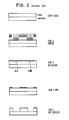
- Figure 2 illustrates schematically another preferred embodiment of the present invention (Scheme IB) wherein vapor phase organometallic treatment occurs after exposure of the resist.
- This invention represents a new dry process utilizing unique surface chemistry combined with dry processing and unique resist compositions useful thereof. The process schemes of two preferred processes are outlined in Figures 1 and 2. This invention also describes the use of organometallic reagents of a specific type and character.
- The reagents and methods of the present invention afford increased resolution ability in resist pattern fabrication due to the fact that only about 2000 Angstroms of the resist film needs to be exposed. This eliminates previous concerns of phenolic absorption in the film. Also based upon this surface chemistry, the aspect ratio and sidewall profile benefit from dry processing.
- It will be recognized by those of ordinary skill in this art that this process relies on unique surface chemistry and is based upon the discovery that certain preferred materials are capable of hydrolyzing the trimethyl silyl group from a poly(p-vinyl) phenol or novolak backbone.
- While the drawings call specifically for one preferred organometallic treatment (i.e., silylation) it is to be understood that this is merely illustrative of the presently most preferred embodiment, and that the alternative organometallic compounds described herein can readily be substituted in the process schemes outlined in the drawings accompanying this disclosure.
- Referring in detail to the drawings, it will be appreciated that, as illustrated in Figure 1, in Scheme IA, a substrate is initially coated with a resist formulation containing a photoacid generator. A thin (e.g., ≦ 2000 Angstrom) layer of silylated resist is formed as in
Step 2. Exposure of this coated resist film to deep U.V. radiation releases the strong photogenerated acid in the exposed areas which desilylates the film in the exposed areas. The silyl hydrolysis products are removed during a postexposure bake out (PEB). For example, when hexamethyldisilazane (HMDS), the preferred silylating agent is employed, the post exposure bake drives out hexamethyl disiloxane, the product of acid hydrolysis. - Dry development of the resulting partially desilylated resist film using a conventional oxygen etch system, affords the desired pattern, a positive tone image.
- As illustrated in Figure 2, Scheme IB is directed to a modification of the Scheme IA process, in which the resist formulation, containing a photoacid generator, is again coated on a substrate, but prior to silylation is subjected to an exposure step. This deep U.V. exposure causes the release of the strong photogenerated acid in the exposed areas. Treatment of this exposed resist with a silylating agent such as hexamethyl disilazane caused selective penetration of only the unexposed areas of the resist film. The photo generated acid prevents silylation in the exposed areas.
- During a postexposure bake (PEB) step, that portion of the resist film wherein the strong photo-generated acid was released (i.e., the exposed areas) is removed.
- Dry development of the resulting partially desilylated resist film using a conventional oxygen etch system, affords the desired pattern, a positive tone image.
- As the acid-hydrolizeable organometallic material employed herein, the skilled artisan will readily recognize that in addition to HMDS, numerous other organometallic compounds of this type are available for use herein.
- One preferred group of such compounds are the tetra-substituted organometallic species. These compounds have the generic formula:
R₁R₂R₃R₄-M
wherein:
M is selected from the group consisting of Si; Sn, Ti, P, Ge, and Zr, preferably Si, and
the organic substituents R₁ - R₄ are each independently selected from the group consisting of alkyl, preferably C₁ - C₁₆, more preferably C₁ - C₁₀, most preferably, C₁ - C₆; aryl, preferably phenyl or alkyl substituted phenyl; and a suitable leaving group such as halogen, preferably Cl, Br, or I. - Similarly, substituted organometallic amine species such as;
(R₁R₂R₃-M)2+x = NH1-x
wherein;
x = 0 or 1;
M is selected from the group consisting of Si, Sn, Ti, Ge, and Zr, preferably Si; and
the organic substituents R₁ - R₃ are each independently selected from the group consisting of alkyl, preferably C₁ - C₁₆, more preferably C₁ - C₁₀, most preferably, C₁ - C₆; and aryl, preferably phenyl, alkyl substituted phenyl;
may be used herein. - As described above, the most preferred compound of this type, HMDS, which is more completely known as 1,1,1,3,3,3-hexamethyldisilazane, has the formula:
(CH₃)₃-Si-NH-Si-(CH₃)₃ - Of the PAGs and PACs useful herein, the skilled artisan will readily be able to select from the available compounds of this type. One preferred class of such PACs are the diazonaphthoquinone sulfonic acid compounds of the type:

Y = O or N; and R is selected from the group consisting of alkyl, preferably C₁ - C₁₆, more preferably C₁ - C₁₀, most preferably, C₁ - C₆; and aryl, preferably phenyl, alkyl substituted phenyl. - One preferred resist formulation of the present invention contains poly(p-vinyl) phenol and as a photoacid generator, a halogenated aromatic compound of the formula:

X = Cl, Br, F, or I;
n is an integer from 1 to 10 inclusive;
m is an integer from 1 to 10 inclusive; and
the organic substituents R₁ - R₃ are each independently selected from the group consisting of alkyl or aryl groups. - Another preferred resist formulation of the present invention contains poly(p-vinyl) phenol and a photoacid generator consisting of halogenated aromatic compounds of the formula:

the substituents R₁ - R₃ are each independently selected from the group consisting of hydrogen, and halogenated (F, Br, Cl, I) alkyl groups. An especially preferred PAG of this type is tris(2,3-dibromopropyl)- isocyanurate. - After mixing the various ingredients in a suitable solvent, the resist formulation is first spin coated and pre-baked.
- In one preferred embodiment of the method of the present invention, the resist film containing either a PAG, a PAC, or mixtures thereof, is then subjected to a thin film treatment by the acid hydrolyzable organometallic compound, i.e., reaction of the organometallic compound with no more than about the first 2000 Angstroms thickness of polymer backbone comprising the film. The remaining thickness of the resist film stays unreacted.
- This thin-film reacted resist film is next exposed with deep UV irradiation. In the exposed areas, a photo-generated acid is produced which causes the hydrolysis of the organometallic species from the poly(p-vinyl) phenol backbone. This leads to break down of the etch mask character of the film in the exposed areas after appropriate post exposure heat treatment.
- Dry development of the baked resist causes break down of the etch mask character in the exposed areas.
- In a second preferred embodiment of the present invention, the PAC/PAG containing resist film described above, is exposed with deep UV radiation prior to the step when the organometallic compound is reacted therewith.
- Exposure of the resist film causes a release of the photo generated acid, which in turn prevents reaction between the polymer backbone of the resist formulation and the organometallic compound in the exposed areas. In this embodiment, the selectivity is built into the organometallic treatment step.
- The present invention will be further illustrated with reference to the following examples which will aid in the understanding of the present invention, but which are not to be construed as a limitation thereof. All percentages reported herein, unless otherwise specified, are percent by weight. All temperatures are expressed in degrees Celsius.
- A positive tone resist pattern was obtained in the following manner:
- A polymeric resist material comprising a mixture of 5.0 g of a photoacid generator (PAG), such as tris(2,3-dibromopropyl)- isocyanurate and 20 g of a novolak resin, such as m-cresol novolak, was formulated with a standard photoresist solvent, such as, propylene glycol or monomethyl ether acetate.
- The resist solution was dispensed in 2.0 ml quantities on a 75 mm wafer to give 1.0 micron coatings upon baking at 80oC for 60 seconds on a hot plate. The resist films were then silylated with hexamethyl disilazane (HMDS) in vapor phase using a commercially available Monarch 150 silylation apparatus. Typical silylating conditions were 150oC for 70 seconds under 100 mtorr of HMDS. The resist was then exposed on an HTG Deep UV contact printer with exposures ranging from 10 to 50 mJ/cm².
- The silylated wafers were next baked at 100oC for 60 seconds on a hot plate. Dry development was done on a Plasma Technologies oxygen reactive ion etcher under the conditions of 20 cc. 0₂, 20 mtorr pressure, 100 watts bias. After 4 minutes, 2.0 micron lines were resolved, with vertical sidewalls. One-half micron of resist was retained. The lines remained where exposed, indicative of a positive tone image.
- Resist compositions were prepared again as in Example 1. The resist solution was dispensed in 2.0 ml quantities on a 75 mm wafer. The composition was subjected to softbake conditions of 80oC for 60 seconds on a hot plate, yielding a resist film. The film coating was then exposed on an HTG deep UV contact printer with exposures ranging from 10 to 50 mJ/cm².
- The exposed wafers were then silylated at 150oC for 35 seconds on a Monarch 150 silylation apparatus. The wafers were then baked at 100oC for 60 seconds on a hot plate. Dry development was conducted on a Plasma Technologies Oxygen reactive ion etcher under the conditions of 20 cc 0₂, 20 mtorr pressure, 100 watts bias.
- After 4 minutes, 3.0 micron lines were resolved, with vertical sidewalls. Where resist remained, there was 0.35 micron resist left. These images constituted a positive image system.
- The present invention has been described in detail, including the preferred embodiments thereof. However, it will be appreciated that those skilled in the art, upon consideration of the present disclosure, may make modifications and/or improvements on this invention and still be within the scope and spirit of this invention as set forth in the following claims.
Claims (33)

X = Cl, Br, F, or I;
n is an integer from 1 to 10 inclusive;
m is an integer from 1 to 10 inclusive; and
the organic substituents R₁ - R₃ are each independently selected from the group consisting of alkyl or aryl groups.

the substituents R₁ - R₃ are each independently selected from the group consisting of hydrogen, and halogenated (F, Br, Cl, I) alkyl groups.
R₁R₂R₃R₄-M
wherein;
M is selected from the group consisting of Si, Sn, Ti, P, Ge, and Zr; and
the organic substituents R₁ - R₄ are each independently selected from the group consisting of alkyl, aryl, and a suitable leaving group, with the proviso that one such substituent is a leaving group.
(R₁R₂R₃-M) 2+x -NH1-x
wherein;
x = 0 or 1;
M is selected from the group consisting of Si, Sn, Ti, Ge, and Zr; and
the organic substituents R₁ - R₃ are each independently selected from the group consisting of alkyl and aryl.

R is selected from the group consisting of alkyl and aryl substituents.
Applications Claiming Priority (2)
| Application Number | Priority Date | Filing Date | Title |
|---|---|---|---|
| US226282 | 1988-07-29 | ||
| US07/226,282 US4921778A (en) | 1988-07-29 | 1988-07-29 | Photoresist pattern fabrication employing chemically amplified metalized material |
Publications (3)
| Publication Number | Publication Date |
|---|---|
| EP0352739A2 true EP0352739A2 (en) | 1990-01-31 |
| EP0352739A3 EP0352739A3 (en) | 1991-09-11 |
| EP0352739B1 EP0352739B1 (en) | 1995-12-27 |
Family
ID=22848289
Family Applications (1)
| Application Number | Title | Priority Date | Filing Date |
|---|---|---|---|
| EP89113699A Expired - Lifetime EP0352739B1 (en) | 1988-07-29 | 1989-07-25 | Photoresist pattern fabrication employing chemically amplified metalized material |
Country Status (4)
| Country | Link |
|---|---|
| US (1) | US4921778A (en) |
| EP (1) | EP0352739B1 (en) |
| JP (1) | JPH02289858A (en) |
| DE (1) | DE68925244T2 (en) |
Cited By (3)
| Publication number | Priority date | Publication date | Assignee | Title |
|---|---|---|---|---|
| EP0410268A2 (en) * | 1989-07-27 | 1991-01-30 | International Business Machines Corporation | Etch resistant pattern formation via interfacial silylation process |
| US5733706A (en) * | 1994-05-25 | 1998-03-31 | Siemens Aktiengesellschaft | Dry-developable positive resist |
| EP0919874A2 (en) * | 1997-11-26 | 1999-06-02 | TRW Inc. | Photoresist composition effective for use as an ion etch barrier after patterning |
Families Citing this family (75)
| Publication number | Priority date | Publication date | Assignee | Title |
|---|---|---|---|---|
| US5108875A (en) * | 1988-07-29 | 1992-04-28 | Shipley Company Inc. | Photoresist pattern fabrication employing chemically amplified metalized material |
| US5079131A (en) * | 1988-08-29 | 1992-01-07 | Shipley Company Inc. | Method of forming positive images through organometallic treatment of negative acid hardening cross-linked photoresist formulations |
| US5041362A (en) * | 1989-07-06 | 1991-08-20 | Texas Instruments Incorporated | Dry developable resist etch chemistry |
| US5316895A (en) * | 1990-10-31 | 1994-05-31 | Texas Instruments Incorporated | Photolithographic method using non-photoactive resins |
| DE59108083D1 (en) * | 1990-12-20 | 1996-09-19 | Siemens Ag | Photolithographic structure generation |
| US5962196A (en) * | 1991-04-08 | 1999-10-05 | Intel Corporation | Deep ultraviolet light photoresist processing |
| US6165697A (en) * | 1991-11-15 | 2000-12-26 | Shipley Company, L.L.C. | Antihalation compositions |
| US6472128B2 (en) | 1996-04-30 | 2002-10-29 | Shipley Company, L.L.C. | Antihalation compositions |
| US6528235B2 (en) | 1991-11-15 | 2003-03-04 | Shipley Company, L.L.C. | Antihalation compositions |
| US6773864B1 (en) * | 1991-11-15 | 2004-08-10 | Shipley Company, L.L.C. | Antihalation compositions |
| US5366852A (en) * | 1992-09-21 | 1994-11-22 | Shipley Company, Inc. | Methods for treating photoresists |
| US5480748A (en) * | 1992-10-21 | 1996-01-02 | International Business Machines Corporation | Protection of aluminum metallization against chemical attack during photoresist development |
| US6117622A (en) * | 1997-09-05 | 2000-09-12 | Fusion Systems Corporation | Controlled shrinkage of photoresist |
| US6057084A (en) * | 1997-10-03 | 2000-05-02 | Fusion Systems Corporation | Controlled amine poisoning for reduced shrinkage of features formed in photoresist |
| US6096484A (en) * | 1997-10-15 | 2000-08-01 | Kabushiki Kaisha Toshiba | Pattern forming method using chemically amplified resist and apparatus for treating chemically amplified resist |
| US6027853A (en) * | 1998-01-16 | 2000-02-22 | Olin Microelectronic Chemicals, Inc. | Process for preparing a radiation-sensitive composition |
| AU3964199A (en) * | 1998-04-07 | 1999-10-25 | Euv Limited Liability Corporation | Thin layer imaging process for microlithography using radiation at strongly attenuated wavelengths |
| KR100804873B1 (en) * | 1999-06-10 | 2008-02-20 | 얼라이드시그날 인코퍼레이티드 | Spin-on-glass anti-reflective coatings for photolithography |
| US6873087B1 (en) * | 1999-10-29 | 2005-03-29 | Board Of Regents, The University Of Texas System | High precision orientation alignment and gap control stages for imprint lithography processes |
| EP2264522A3 (en) * | 2000-07-16 | 2011-12-14 | The Board of Regents of The University of Texas System | Method of forming a pattern on a substrate |
| WO2002006902A2 (en) | 2000-07-17 | 2002-01-24 | Board Of Regents, The University Of Texas System | Method and system of automatic fluid dispensing for imprint lithography processes |
| US6368400B1 (en) * | 2000-07-17 | 2002-04-09 | Honeywell International | Absorbing compounds for spin-on-glass anti-reflective coatings for photolithography |
| KR20030040378A (en) * | 2000-08-01 | 2003-05-22 | 보드 오브 리전츠, 더 유니버시티 오브 텍사스 시스템 | Methods for high-precision gap and orientation sensing between a transparent template and substrate for imprint lithography |
| AU2001286573A1 (en) * | 2000-08-21 | 2002-03-04 | Board Of Regents, The University Of Texas System | Flexure based macro motion translation stage |
| WO2002067055A2 (en) * | 2000-10-12 | 2002-08-29 | Board Of Regents, The University Of Texas System | Template for room temperature, low pressure micro- and nano-imprint lithography |
| US20050274219A1 (en) * | 2004-06-01 | 2005-12-15 | Molecular Imprints, Inc. | Method and system to control movement of a body for nano-scale manufacturing |
| US6605519B2 (en) * | 2001-05-02 | 2003-08-12 | Unaxis Usa, Inc. | Method for thin film lift-off processes using lateral extended etching masks and device |
| US6964793B2 (en) * | 2002-05-16 | 2005-11-15 | Board Of Regents, The University Of Texas System | Method for fabricating nanoscale patterns in light curable compositions using an electric field |
| US7037639B2 (en) * | 2002-05-01 | 2006-05-02 | Molecular Imprints, Inc. | Methods of manufacturing a lithography template |
| US20030235787A1 (en) * | 2002-06-24 | 2003-12-25 | Watts Michael P.C. | Low viscosity high resolution patterning material |
| US6926929B2 (en) | 2002-07-09 | 2005-08-09 | Molecular Imprints, Inc. | System and method for dispensing liquids |
| US6900881B2 (en) | 2002-07-11 | 2005-05-31 | Molecular Imprints, Inc. | Step and repeat imprint lithography systems |
| US7077992B2 (en) | 2002-07-11 | 2006-07-18 | Molecular Imprints, Inc. | Step and repeat imprint lithography processes |
| US6932934B2 (en) | 2002-07-11 | 2005-08-23 | Molecular Imprints, Inc. | Formation of discontinuous films during an imprint lithography process |
| US6908861B2 (en) * | 2002-07-11 | 2005-06-21 | Molecular Imprints, Inc. | Method for imprint lithography using an electric field |
| US7019819B2 (en) | 2002-11-13 | 2006-03-28 | Molecular Imprints, Inc. | Chucking system for modulating shapes of substrates |
| US7070405B2 (en) * | 2002-08-01 | 2006-07-04 | Molecular Imprints, Inc. | Alignment systems for imprint lithography |
| US7027156B2 (en) | 2002-08-01 | 2006-04-11 | Molecular Imprints, Inc. | Scatterometry alignment for imprint lithography |
| US6916584B2 (en) | 2002-08-01 | 2005-07-12 | Molecular Imprints, Inc. | Alignment methods for imprint lithography |
| US7071088B2 (en) * | 2002-08-23 | 2006-07-04 | Molecular Imprints, Inc. | Method for fabricating bulbous-shaped vias |
| US8349241B2 (en) | 2002-10-04 | 2013-01-08 | Molecular Imprints, Inc. | Method to arrange features on a substrate to replicate features having minimal dimensional variability |
| US6980282B2 (en) | 2002-12-11 | 2005-12-27 | Molecular Imprints, Inc. | Method for modulating shapes of substrates |
| US6929762B2 (en) * | 2002-11-13 | 2005-08-16 | Molecular Imprints, Inc. | Method of reducing pattern distortions during imprint lithography processes |
| US6871558B2 (en) * | 2002-12-12 | 2005-03-29 | Molecular Imprints, Inc. | Method for determining characteristics of substrate employing fluid geometries |
| US7452574B2 (en) * | 2003-02-27 | 2008-11-18 | Molecular Imprints, Inc. | Method to reduce adhesion between a polymerizable layer and a substrate employing a fluorine-containing layer |
| US7179396B2 (en) * | 2003-03-25 | 2007-02-20 | Molecular Imprints, Inc. | Positive tone bi-layer imprint lithography method |
| US7122079B2 (en) | 2004-02-27 | 2006-10-17 | Molecular Imprints, Inc. | Composition for an etching mask comprising a silicon-containing material |
| US7396475B2 (en) * | 2003-04-25 | 2008-07-08 | Molecular Imprints, Inc. | Method of forming stepped structures employing imprint lithography |
| US7223518B2 (en) * | 2003-06-06 | 2007-05-29 | Georgia Tech Research Corporation | Compositions and methods of use thereof |
| US7157036B2 (en) | 2003-06-17 | 2007-01-02 | Molecular Imprints, Inc | Method to reduce adhesion between a conformable region and a pattern of a mold |
| US7136150B2 (en) * | 2003-09-25 | 2006-11-14 | Molecular Imprints, Inc. | Imprint lithography template having opaque alignment marks |
| US7090716B2 (en) * | 2003-10-02 | 2006-08-15 | Molecular Imprints, Inc. | Single phase fluid imprint lithography method |
| US8211214B2 (en) * | 2003-10-02 | 2012-07-03 | Molecular Imprints, Inc. | Single phase fluid imprint lithography method |
| US20050084804A1 (en) * | 2003-10-16 | 2005-04-21 | Molecular Imprints, Inc. | Low surface energy templates |
| US8053159B2 (en) | 2003-11-18 | 2011-11-08 | Honeywell International Inc. | Antireflective coatings for via fill and photolithography applications and methods of preparation thereof |
| US8076386B2 (en) | 2004-02-23 | 2011-12-13 | Molecular Imprints, Inc. | Materials for imprint lithography |
| US7906180B2 (en) | 2004-02-27 | 2011-03-15 | Molecular Imprints, Inc. | Composition for an etching mask comprising a silicon-containing material |
| US20050275311A1 (en) * | 2004-06-01 | 2005-12-15 | Molecular Imprints, Inc. | Compliant device for nano-scale manufacturing |
| US20060145398A1 (en) * | 2004-12-30 | 2006-07-06 | Board Of Regents, The University Of Texas System | Release layer comprising diamond-like carbon (DLC) or doped DLC with tunable composition for imprint lithography templates and contact masks |
| US7906058B2 (en) * | 2005-12-01 | 2011-03-15 | Molecular Imprints, Inc. | Bifurcated contact printing technique |
| US7803308B2 (en) * | 2005-12-01 | 2010-09-28 | Molecular Imprints, Inc. | Technique for separating a mold from solidified imprinting material |
| JP4987012B2 (en) * | 2005-12-08 | 2012-07-25 | モレキュラー・インプリンツ・インコーポレーテッド | Method and system for patterning both sides of a substrate |
| US7670530B2 (en) * | 2006-01-20 | 2010-03-02 | Molecular Imprints, Inc. | Patterning substrates employing multiple chucks |
| WO2007117524A2 (en) * | 2006-04-03 | 2007-10-18 | Molecular Imprints, Inc. | Method of concurrently patterning a substrate having a plurality of fields and alignment marks |
| US8850980B2 (en) | 2006-04-03 | 2014-10-07 | Canon Nanotechnologies, Inc. | Tessellated patterns in imprint lithography |
| US8142850B2 (en) | 2006-04-03 | 2012-03-27 | Molecular Imprints, Inc. | Patterning a plurality of fields on a substrate to compensate for differing evaporation times |
| US7802978B2 (en) | 2006-04-03 | 2010-09-28 | Molecular Imprints, Inc. | Imprinting of partial fields at the edge of the wafer |
| US7547398B2 (en) * | 2006-04-18 | 2009-06-16 | Molecular Imprints, Inc. | Self-aligned process for fabricating imprint templates containing variously etched features |
| US8012395B2 (en) * | 2006-04-18 | 2011-09-06 | Molecular Imprints, Inc. | Template having alignment marks formed of contrast material |
| US8642246B2 (en) | 2007-02-26 | 2014-02-04 | Honeywell International Inc. | Compositions, coatings and films for tri-layer patterning applications and methods of preparation thereof |
| US8557877B2 (en) | 2009-06-10 | 2013-10-15 | Honeywell International Inc. | Anti-reflective coatings for optically transparent substrates |
| US8864898B2 (en) | 2011-05-31 | 2014-10-21 | Honeywell International Inc. | Coating formulations for optical elements |
| WO2014159427A1 (en) | 2013-03-14 | 2014-10-02 | Applied Materials, Inc | Resist hardening and development processes for semiconductor device manufacturing |
| JP6196739B2 (en) | 2014-01-28 | 2017-09-13 | 東京エレクトロン株式会社 | Method for self-aligned double patterning without atomic layer deposition |
| EP3194502A4 (en) | 2015-04-13 | 2018-05-16 | Honeywell International Inc. | Polysiloxane formulations and coatings for optoelectronic applications |
Citations (3)
| Publication number | Priority date | Publication date | Assignee | Title |
|---|---|---|---|---|
| EP0204253A2 (en) * | 1985-06-06 | 1986-12-10 | International Business Machines Corporation | Formation of etch-resistant resists through preferential permeation |
| EP0232973A2 (en) * | 1986-01-13 | 1987-08-19 | Rohm And Haas Company | Microplastic structures, process for forming such structures, and photomask suitable for use in such process |
| US4842986A (en) * | 1985-07-26 | 1989-06-27 | Fuji Photo Film Co., Ltd. | Positively working resist material |
Family Cites Families (9)
| Publication number | Priority date | Publication date | Assignee | Title |
|---|---|---|---|---|
| JPS5723937A (en) * | 1980-07-17 | 1982-02-08 | Matsushita Electric Ind Co Ltd | Photographic etching method |
| US4396704A (en) * | 1981-04-22 | 1983-08-02 | Bell Telephone Laboratories, Incorporated | Solid state devices produced by organometallic plasma developed resists |
| US4357369A (en) * | 1981-11-10 | 1982-11-02 | Rca Corporation | Method of plasma etching a substrate |
| EP0091651B1 (en) * | 1982-04-12 | 1988-08-03 | Nippon Telegraph And Telephone Corporation | Method for forming micropattern |
| US4433044A (en) * | 1982-11-15 | 1984-02-21 | Rca Corporation | Dry developable positive photoresists |
| US4430153A (en) * | 1983-06-30 | 1984-02-07 | International Business Machines Corporation | Method of forming an RIE etch barrier by in situ conversion of a silicon containing alkyl polyamide/polyimide |
| US4552833A (en) * | 1984-05-14 | 1985-11-12 | International Business Machines Corporation | Radiation sensitive and oxygen plasma developable resist |
| JPS6144715A (en) * | 1984-08-08 | 1986-03-04 | Toyo Soda Mfg Co Ltd | Production of molded synthetic mordenite article |
| JPS61227027A (en) * | 1985-04-02 | 1986-10-09 | Kakuichi Technical Dev Service Kk | Production of flexible tube |
-
1988
- 1988-07-29 US US07/226,282 patent/US4921778A/en not_active Expired - Fee Related
-
1989
- 1989-07-25 EP EP89113699A patent/EP0352739B1/en not_active Expired - Lifetime
- 1989-07-25 DE DE68925244T patent/DE68925244T2/en not_active Expired - Fee Related
- 1989-07-29 JP JP1197906A patent/JPH02289858A/en active Pending
Patent Citations (3)
| Publication number | Priority date | Publication date | Assignee | Title |
|---|---|---|---|---|
| EP0204253A2 (en) * | 1985-06-06 | 1986-12-10 | International Business Machines Corporation | Formation of etch-resistant resists through preferential permeation |
| US4842986A (en) * | 1985-07-26 | 1989-06-27 | Fuji Photo Film Co., Ltd. | Positively working resist material |
| EP0232973A2 (en) * | 1986-01-13 | 1987-08-19 | Rohm And Haas Company | Microplastic structures, process for forming such structures, and photomask suitable for use in such process |
Non-Patent Citations (1)
| Title |
|---|
| MICROELECTRONIC ENGINEERING. vol. 6, no. 1-4, December 1987, AMSTERDAM NL pages 393 - 398; K.J. Orvek et al: "An Organosilicon Photoresist for Use in Excimer Laser Lithography" * |
Cited By (5)
| Publication number | Priority date | Publication date | Assignee | Title |
|---|---|---|---|---|
| EP0410268A2 (en) * | 1989-07-27 | 1991-01-30 | International Business Machines Corporation | Etch resistant pattern formation via interfacial silylation process |
| EP0410268A3 (en) * | 1989-07-27 | 1991-10-09 | International Business Machines Corporation | Etch resistant pattern formation via interfacial silylation process |
| US5733706A (en) * | 1994-05-25 | 1998-03-31 | Siemens Aktiengesellschaft | Dry-developable positive resist |
| EP0919874A2 (en) * | 1997-11-26 | 1999-06-02 | TRW Inc. | Photoresist composition effective for use as an ion etch barrier after patterning |
| EP0919874A3 (en) * | 1997-11-26 | 2000-06-07 | TRW Inc. | Photoresist composition effective for use as an ion etch barrier after patterning |
Also Published As
| Publication number | Publication date |
|---|---|
| DE68925244T2 (en) | 1996-08-14 |
| EP0352739A3 (en) | 1991-09-11 |
| JPH02289858A (en) | 1990-11-29 |
| EP0352739B1 (en) | 1995-12-27 |
| DE68925244D1 (en) | 1996-02-08 |
| US4921778A (en) | 1990-05-01 |
Similar Documents
| Publication | Publication Date | Title |
|---|---|---|
| EP0352739B1 (en) | Photoresist pattern fabrication employing chemically amplified metalized material | |
| US5108875A (en) | Photoresist pattern fabrication employing chemically amplified metalized material | |
| KR100212933B1 (en) | Positive resist composition | |
| US4931351A (en) | Bilayer lithographic process | |
| EP1810084B1 (en) | Resist composition | |
| US5691396A (en) | Polysiloxane compounds and positive resist compositions | |
| EP0493367B1 (en) | Silane resist materials and method for their preparation | |
| EP1660561B1 (en) | Photosensitive silsesquioxane resin | |
| EP2376584B1 (en) | Wet-etchable antireflective coatings | |
| KR100754230B1 (en) | Radiation sensitive copolymers, photoresist compositions thereof and deep UV bilayer systems thereof | |
| EP0758102A1 (en) | Terpolymers containing organosilicon side chains and their use for the production of relief structures | |
| KR101690159B1 (en) | Switchable Antireflective Coatings | |
| JPH0369101B2 (en) | ||
| US5384220A (en) | Production of photolithographic structures | |
| JP2004519734A (en) | Silicon-containing acetal protective polymer and photoresist composition thereof | |
| US5079131A (en) | Method of forming positive images through organometallic treatment of negative acid hardening cross-linked photoresist formulations | |
| KR100398312B1 (en) | Organometal-containing norbornene monomer, photoresist containing its polymer, manufacturing methods thereof, and method of forming photoresist patterns | |
| JPH11186243A (en) | Method of etching silicon oxide silicon layer | |
| EP0274757A2 (en) | Bilayer lithographic process | |
| JP3414708B2 (en) | Method of forming patterned polysilazane film | |
| US20200292940A1 (en) | Silsesquioxane composition with both positive and negative photo resist characteristics | |
| JP2828572B2 (en) | Tertiary butyl ester diphenolic acid derivative and positive resist material containing the same | |
| JP3695486B2 (en) | Chemically amplified positive resist material and method for producing the same | |
| JP2001288270A (en) | Modified polysil sesquiazane, photosensitive composition, and method for forming patterned modified polysil sesquiazane film | |
| JP2004053838A (en) | Photosensitive composition for interlayer insulating film and method for forming patterned interlayer insulating film |
Legal Events
| Date | Code | Title | Description |
|---|---|---|---|
| PUAI | Public reference made under article 153(3) epc to a published international application that has entered the european phase |
Free format text: ORIGINAL CODE: 0009012 |
|
| AK | Designated contracting states |
Kind code of ref document: A2 Designated state(s): DE FR GB IT |
|
| PUAL | Search report despatched |
Free format text: ORIGINAL CODE: 0009013 |
|
| AK | Designated contracting states |
Kind code of ref document: A3 Designated state(s): DE FR GB IT |
|
| 17P | Request for examination filed |
Effective date: 19920110 |
|
| 17Q | First examination report despatched |
Effective date: 19940429 |
|
| GRAA | (expected) grant |
Free format text: ORIGINAL CODE: 0009210 |
|
| AK | Designated contracting states |
Kind code of ref document: B1 Designated state(s): DE FR GB IT |
|
| REF | Corresponds to: |
Ref document number: 68925244 Country of ref document: DE Date of ref document: 19960208 |
|
| ITF | It: translation for a ep patent filed |
Owner name: DR. ING. A. RACHELI & C. |
|
| ET | Fr: translation filed | ||
| PGFP | Annual fee paid to national office [announced via postgrant information from national office to epo] |
Ref country code: GB Payment date: 19960710 Year of fee payment: 8 |
|
| PGFP | Annual fee paid to national office [announced via postgrant information from national office to epo] |
Ref country code: FR Payment date: 19960719 Year of fee payment: 8 |
|
| PGFP | Annual fee paid to national office [announced via postgrant information from national office to epo] |
Ref country code: DE Payment date: 19960925 Year of fee payment: 8 |
|
| PLBE | No opposition filed within time limit |
Free format text: ORIGINAL CODE: 0009261 |
|
| STAA | Information on the status of an ep patent application or granted ep patent |
Free format text: STATUS: NO OPPOSITION FILED WITHIN TIME LIMIT |
|
| 26N | No opposition filed | ||
| PG25 | Lapsed in a contracting state [announced via postgrant information from national office to epo] |
Ref country code: GB Free format text: LAPSE BECAUSE OF NON-PAYMENT OF DUE FEES Effective date: 19970725 |
|
| GBPC | Gb: european patent ceased through non-payment of renewal fee |
Effective date: 19970725 |
|
| PG25 | Lapsed in a contracting state [announced via postgrant information from national office to epo] |
Ref country code: FR Free format text: LAPSE BECAUSE OF NON-PAYMENT OF DUE FEES Effective date: 19980331 |
|
| PG25 | Lapsed in a contracting state [announced via postgrant information from national office to epo] |
Ref country code: DE Free format text: LAPSE BECAUSE OF NON-PAYMENT OF DUE FEES Effective date: 19980401 |
|
| REG | Reference to a national code |
Ref country code: FR Ref legal event code: ST |
|
| PG25 | Lapsed in a contracting state [announced via postgrant information from national office to epo] |
Ref country code: IT Free format text: LAPSE BECAUSE OF NON-PAYMENT OF DUE FEES;WARNING: LAPSES OF ITALIAN PATENTS WITH EFFECTIVE DATE BEFORE 2007 MAY HAVE OCCURRED AT ANY TIME BEFORE 2007. THE CORRECT EFFECTIVE DATE MAY BE DIFFERENT FROM THE ONE RECORDED. Effective date: 20050725 |