EP0350179B1 - Manufacturing portable electronic tokens - Google Patents
Manufacturing portable electronic tokens Download PDFInfo
- Publication number
- EP0350179B1 EP0350179B1 EP89306256A EP89306256A EP0350179B1 EP 0350179 B1 EP0350179 B1 EP 0350179B1 EP 89306256 A EP89306256 A EP 89306256A EP 89306256 A EP89306256 A EP 89306256A EP 0350179 B1 EP0350179 B1 EP 0350179B1
- Authority
- EP
- European Patent Office
- Prior art keywords
- members
- mould
- components
- token
- output means
- Prior art date
- Legal status (The legal status is an assumption and is not a legal conclusion. Google has not performed a legal analysis and makes no representation as to the accuracy of the status listed.)
- Expired - Lifetime
Links
Images

Classifications
-
- B—PERFORMING OPERATIONS; TRANSPORTING
- B32—LAYERED PRODUCTS
- B32B—LAYERED PRODUCTS, i.e. PRODUCTS BUILT-UP OF STRATA OF FLAT OR NON-FLAT, e.g. CELLULAR OR HONEYCOMB, FORM
- B32B37/00—Methods or apparatus for laminating, e.g. by curing or by ultrasonic bonding
- B32B37/14—Methods or apparatus for laminating, e.g. by curing or by ultrasonic bonding characterised by the properties of the layers
- B32B37/16—Methods or apparatus for laminating, e.g. by curing or by ultrasonic bonding characterised by the properties of the layers with all layers existing as coherent layers before laminating
- B32B37/22—Methods or apparatus for laminating, e.g. by curing or by ultrasonic bonding characterised by the properties of the layers with all layers existing as coherent layers before laminating involving the assembly of both discrete and continuous layers
- B32B37/223—One or more of the layers being plastic
- B32B37/226—Laminating sheets, panels or inserts between two continuous plastic layers
-
- G—PHYSICS
- G06—COMPUTING; CALCULATING OR COUNTING
- G06K—GRAPHICAL DATA READING; PRESENTATION OF DATA; RECORD CARRIERS; HANDLING RECORD CARRIERS
- G06K19/00—Record carriers for use with machines and with at least a part designed to carry digital markings
- G06K19/06—Record carriers for use with machines and with at least a part designed to carry digital markings characterised by the kind of the digital marking, e.g. shape, nature, code
-
- B—PERFORMING OPERATIONS; TRANSPORTING
- B29—WORKING OF PLASTICS; WORKING OF SUBSTANCES IN A PLASTIC STATE IN GENERAL
- B29C—SHAPING OR JOINING OF PLASTICS; SHAPING OF MATERIAL IN A PLASTIC STATE, NOT OTHERWISE PROVIDED FOR; AFTER-TREATMENT OF THE SHAPED PRODUCTS, e.g. REPAIRING
- B29C33/00—Moulds or cores; Details thereof or accessories therefor
- B29C33/34—Moulds or cores; Details thereof or accessories therefor movable, e.g. to or from the moulding station
- B29C33/36—Moulds or cores; Details thereof or accessories therefor movable, e.g. to or from the moulding station continuously movable in one direction, e.g. in a closed circuit
-
- B—PERFORMING OPERATIONS; TRANSPORTING
- B29—WORKING OF PLASTICS; WORKING OF SUBSTANCES IN A PLASTIC STATE IN GENERAL
- B29C—SHAPING OR JOINING OF PLASTICS; SHAPING OF MATERIAL IN A PLASTIC STATE, NOT OTHERWISE PROVIDED FOR; AFTER-TREATMENT OF THE SHAPED PRODUCTS, e.g. REPAIRING
- B29C33/00—Moulds or cores; Details thereof or accessories therefor
- B29C33/56—Coatings, e.g. enameled or galvanised; Releasing, lubricating or separating agents
- B29C33/68—Release sheets
-
- B—PERFORMING OPERATIONS; TRANSPORTING
- B29—WORKING OF PLASTICS; WORKING OF SUBSTANCES IN A PLASTIC STATE IN GENERAL
- B29C—SHAPING OR JOINING OF PLASTICS; SHAPING OF MATERIAL IN A PLASTIC STATE, NOT OTHERWISE PROVIDED FOR; AFTER-TREATMENT OF THE SHAPED PRODUCTS, e.g. REPAIRING
- B29C70/00—Shaping composites, i.e. plastics material comprising reinforcements, fillers or preformed parts, e.g. inserts
- B29C70/68—Shaping composites, i.e. plastics material comprising reinforcements, fillers or preformed parts, e.g. inserts by incorporating or moulding on preformed parts, e.g. inserts or layers, e.g. foam blocks
- B29C70/70—Completely encapsulating inserts
-
- G—PHYSICS
- G06—COMPUTING; CALCULATING OR COUNTING
- G06K—GRAPHICAL DATA READING; PRESENTATION OF DATA; RECORD CARRIERS; HANDLING RECORD CARRIERS
- G06K19/00—Record carriers for use with machines and with at least a part designed to carry digital markings
- G06K19/06—Record carriers for use with machines and with at least a part designed to carry digital markings characterised by the kind of the digital marking, e.g. shape, nature, code
- G06K19/067—Record carriers with conductive marks, printed circuits or semiconductor circuit elements, e.g. credit or identity cards also with resonating or responding marks without active components
- G06K19/07—Record carriers with conductive marks, printed circuits or semiconductor circuit elements, e.g. credit or identity cards also with resonating or responding marks without active components with integrated circuit chips
- G06K19/077—Constructional details, e.g. mounting of circuits in the carrier
- G06K19/07718—Constructional details, e.g. mounting of circuits in the carrier the record carrier being manufactured in a continuous process, e.g. using endless rolls
-
- G—PHYSICS
- G06—COMPUTING; CALCULATING OR COUNTING
- G06K—GRAPHICAL DATA READING; PRESENTATION OF DATA; RECORD CARRIERS; HANDLING RECORD CARRIERS
- G06K19/00—Record carriers for use with machines and with at least a part designed to carry digital markings
- G06K19/06—Record carriers for use with machines and with at least a part designed to carry digital markings characterised by the kind of the digital marking, e.g. shape, nature, code
- G06K19/067—Record carriers with conductive marks, printed circuits or semiconductor circuit elements, e.g. credit or identity cards also with resonating or responding marks without active components
- G06K19/07—Record carriers with conductive marks, printed circuits or semiconductor circuit elements, e.g. credit or identity cards also with resonating or responding marks without active components with integrated circuit chips
- G06K19/077—Constructional details, e.g. mounting of circuits in the carrier
- G06K19/0772—Physical layout of the record carrier
- G06K19/07728—Physical layout of the record carrier the record carrier comprising means for protection against impact or bending, e.g. protective shells or stress-absorbing layers around the integrated circuit
-
- G—PHYSICS
- G06—COMPUTING; CALCULATING OR COUNTING
- G06K—GRAPHICAL DATA READING; PRESENTATION OF DATA; RECORD CARRIERS; HANDLING RECORD CARRIERS
- G06K19/00—Record carriers for use with machines and with at least a part designed to carry digital markings
- G06K19/06—Record carriers for use with machines and with at least a part designed to carry digital markings characterised by the kind of the digital marking, e.g. shape, nature, code
- G06K19/067—Record carriers with conductive marks, printed circuits or semiconductor circuit elements, e.g. credit or identity cards also with resonating or responding marks without active components
- G06K19/07—Record carriers with conductive marks, printed circuits or semiconductor circuit elements, e.g. credit or identity cards also with resonating or responding marks without active components with integrated circuit chips
- G06K19/077—Constructional details, e.g. mounting of circuits in the carrier
- G06K19/07745—Mounting details of integrated circuit chips
-
- G—PHYSICS
- G06—COMPUTING; CALCULATING OR COUNTING
- G06K—GRAPHICAL DATA READING; PRESENTATION OF DATA; RECORD CARRIERS; HANDLING RECORD CARRIERS
- G06K19/00—Record carriers for use with machines and with at least a part designed to carry digital markings
- G06K19/06—Record carriers for use with machines and with at least a part designed to carry digital markings characterised by the kind of the digital marking, e.g. shape, nature, code
- G06K19/067—Record carriers with conductive marks, printed circuits or semiconductor circuit elements, e.g. credit or identity cards also with resonating or responding marks without active components
- G06K19/07—Record carriers with conductive marks, printed circuits or semiconductor circuit elements, e.g. credit or identity cards also with resonating or responding marks without active components with integrated circuit chips
- G06K19/077—Constructional details, e.g. mounting of circuits in the carrier
- G06K19/07749—Constructional details, e.g. mounting of circuits in the carrier the record carrier being capable of non-contact communication, e.g. constructional details of the antenna of a non-contact smart card
-
- B—PERFORMING OPERATIONS; TRANSPORTING
- B29—WORKING OF PLASTICS; WORKING OF SUBSTANCES IN A PLASTIC STATE IN GENERAL
- B29C—SHAPING OR JOINING OF PLASTICS; SHAPING OF MATERIAL IN A PLASTIC STATE, NOT OTHERWISE PROVIDED FOR; AFTER-TREATMENT OF THE SHAPED PRODUCTS, e.g. REPAIRING
- B29C67/00—Shaping techniques not covered by groups B29C39/00 - B29C65/00, B29C70/00 or B29C73/00
- B29C67/24—Shaping techniques not covered by groups B29C39/00 - B29C65/00, B29C70/00 or B29C73/00 characterised by the choice of material
- B29C67/246—Moulding high reactive monomers or prepolymers, e.g. by reaction injection moulding [RIM], liquid injection moulding [LIM]
-
- H—ELECTRICITY
- H01—ELECTRIC ELEMENTS
- H01L—SEMICONDUCTOR DEVICES NOT COVERED BY CLASS H10
- H01L2924/00—Indexing scheme for arrangements or methods for connecting or disconnecting semiconductor or solid-state bodies as covered by H01L24/00
- H01L2924/0001—Technical content checked by a classifier
- H01L2924/0002—Not covered by any one of groups H01L24/00, H01L24/00 and H01L2224/00
-
- H—ELECTRICITY
- H05—ELECTRIC TECHNIQUES NOT OTHERWISE PROVIDED FOR
- H05K—PRINTED CIRCUITS; CASINGS OR CONSTRUCTIONAL DETAILS OF ELECTRIC APPARATUS; MANUFACTURE OF ASSEMBLAGES OF ELECTRICAL COMPONENTS
- H05K1/00—Printed circuits
- H05K1/02—Details
- H05K1/0271—Arrangements for reducing stress or warp in rigid printed circuit boards, e.g. caused by loads, vibrations or differences in thermal expansion
-
- H—ELECTRICITY
- H05—ELECTRIC TECHNIQUES NOT OTHERWISE PROVIDED FOR
- H05K—PRINTED CIRCUITS; CASINGS OR CONSTRUCTIONAL DETAILS OF ELECTRIC APPARATUS; MANUFACTURE OF ASSEMBLAGES OF ELECTRICAL COMPONENTS
- H05K1/00—Printed circuits
- H05K1/18—Printed circuits structurally associated with non-printed electric components
- H05K1/189—Printed circuits structurally associated with non-printed electric components characterised by the use of a flexible or folded printed circuit
-
- H—ELECTRICITY
- H05—ELECTRIC TECHNIQUES NOT OTHERWISE PROVIDED FOR
- H05K—PRINTED CIRCUITS; CASINGS OR CONSTRUCTIONAL DETAILS OF ELECTRIC APPARATUS; MANUFACTURE OF ASSEMBLAGES OF ELECTRICAL COMPONENTS
- H05K3/00—Apparatus or processes for manufacturing printed circuits
- H05K3/22—Secondary treatment of printed circuits
- H05K3/28—Applying non-metallic protective coatings
- H05K3/284—Applying non-metallic protective coatings for encapsulating mounted components
Abstract
Description
- This invention relates to manufacturing portable electronic tokens and in particular, but not exclusively, it relates to the manufacture of small, portable, articles which include an electronic circuit encapsulated within a plastics material, such as an electronic token of the "smart card" type.
- Injection moulding is often used as a method of manufacturing small plastic articles. In such methods, usually small granules of the plastics material are heated so as to melt the material and the resulting fluid is injected at high temperature and pressure, perhaps 300°C and 2,00 PSI (1 PSI ≈ 6895 Pa) into a mould of a desired shape. The material is then allowed to set in the mould as it cools.
- Such a method is fine for the manufacture of small, homogeneous, articles. However, articles such as those commonly known as "smart cards" which comprises a number of components such as electronic circuits, input/output interfaces, substrates and labels are less well suited to the process since the high pressures and temperatures involved tend to displace inserts and indeed can damage the functioning thereof.
- Research Disclosure, No. 290, June 1988, page 418, abstract No. 29089, New York, NY, US; entitled "Integrated circuit encapsulation by reaction injection moulding" describes a moulding process for the encapsulation of in line tape automatic bonded products such as IC's wherein individual IC's are packaged by encapsulation in plastics material.
- Smart cards are generally manufactured by a lamination process. The present invention seeks to provide an improved moulding technique for articles of this kind.
- According to the present invention, there is provided a method of manufacturing portable electronic tokens such as smart cards, each token comprising one or more electronic components and data input/output means encapsulated within a plastics body and having high tensile modulus members disposed as skins on at least two opposing main faces of the body and having graphics thereon; which method comprises locating two high tensile members against respective sides of a mould, locating the components and data input/output means between the members, injecting a reaction injection mouldable plastics material into the mould such that it encapsulates the components and input/output means and thus forms the plastics body of the token but is prevented, by the members, from contacting the surfaces of the mould, allowing the material to harden, and, removing the token from the mould.
- Preferably, the articles are electronic tokens of the "smart card" type and have credit card sized dimensions, typically 8.5 by 5.4 by 0.075 cm. They may be of the type which use contactless coupling by means of an inductive loop, encapsulated within the plastics or resin material. In one embodiment, the portions of the token are co-extruded. The mould may comprise two endless belts which are located to cooperate in use to form a continuously moving mould cavity.
- In an alternative embodiment, the high tensile members are arranged in two continuous sheets and are transported through the moulds, carrying the components and plastics material; the individual tokens being subsequently separated after hardening.
- Preferably, after the components and plastics material have been introduced between the members, the edges of the members are sealed to form a sealed structure within which the plastics material is allowed to harden. To protect the graphics on the labels or skins, the graphics may be printed or otherwise deposited on their inner surface, i.e. the surface contacting the plastics material. The provision of the skins serves both to strengthen a card, as the skin is of a sufficiently high tensile modulus as to make a card substantially rigid but flexible, typically of similar flexibility and rigidity to a standard laminated credit card, and also serves as a mould release agent since the plastics material, which may for example be an epoxy, has an adhesive nature and thus problems can arise if this contacts the mould and adheres to it.
- Any plastics material or mixture may be used which has the capability of hardening under a reaction injection moulding (RIM) process.
- An embodiment of the invention will now be described by way of example only with reference to the accompanying Figures in which;
- Figure 1 shows schematically the cross section of an electronic token when manufactured by a method embodying the present invention, and;
- Figures 2 and 3 show schematically manufacturing processes.
- Referring to Figure 1, the token or card incorporates one or more integrated
circuits 1 andcapacitors 2. Rigid inserts 3, which may be made of strong metal or a rigid moulded compound, surround the circuits and capacitors so as to provide strengthening and to resist damage caused by flexing the card. The power and input/output requirements of such a card are achieved by means ofinductive coils 4 mounted on asubstrate 5 and disposed generally around the periphery of the card. Printedlabels 6 are positioned on the face of the card. These labels are made of polyester, polycarbonate, polyimide or a material of a similar tensile modulus and, in addition to their function as labels, also have a strengthening effect due to a 'double-skinned' effect. Without the labels the cards might be flaccid and their functions would probably be impaired. The printing is preferably on the inner surface 6a of the label to protect it. The electronic components within the card are inter-connected by means of for example copper layers 7. The remainder of the material of the card is made from a moulded plastics or resin material such as polyurethane 8 or epoxy. - The card is assembled by means of a moulding process known as reaction injection moulding (RIM). This is a well known process which is often used in the manufacture of large plastics articles such as car bumpers, surfboards and the like. The difference from conventional injection moulding techniques is that two materials are used which are combined immediately before moulding. These are a resin and a hardener which, when combined together harden within a fixed time period which is dependent upon the constituents. With conventional injection moulding, heat and pressure are required to melt the resin and inject it into a mould, whereupon the resin sets as it cools. RIM is characterised by the fact that since the resin and hardener mixture is a liquid at a low temperature then high pressure and temperatures are not required.
- In a first embodiment of the present invention the components of the card, other than the liquid plastics material are fixed in place within a mould such that the labels are adjacent the sides of the mould, printed surface inward, and the other components lie between the labels. The resin is then added at a low pressure and temperature. Since the resin is in a fluid state, typically having the consistency of for example milk or thin cream, then the resin flows throughout the mould, making good contact with all the components and eventually completely covering and encapsulating them. It then begins to set after the fixed time period, perhaps two to ten minutes, although resins are available which can begin to set after a few seconds. After the resin has set then the complete token is removed from the mould and the process can be repeated.
- Since the resin is not allowed to contact the mould walls the labels act as a release from the mould cavity walls.
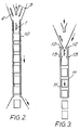
- In order to speed up the production rate, the preprinted labels and components can be fed into a die which is also supplied with RIM fluid resin from a nozzle. This is shown in Figure 2 (which is not to scale), in which the die consists of two recessed endless belts running back to back to form a continuously moving mould cavity or a plurality of
cavities 10, as shown, moving in the direction shown by the arrows. Thelabels 6 andcomponents 1 are fed into the or each moving cavity and the resin fed in through anozzle 9 the resin setting and hardening in the mould cavity or cavities as the belts move. The components, labels and fluid, in the required configuration, are then coextruded from the die to form continuous strips of completed cards, which subsequently set and are then separated as desired. - Figure 3 shows an alternative process in which the
labels 6 are arranged in two continuous sheets which are spooled through amould 11. The edges of the continuous sheets are sealed together by pinch rollers. The resin and components are applied to the labels in the same relative disposition as that of Figure 2. It will be appreciated that, when the mould cavity is defined by endless belts (as described in relation to Figure 2), the labels, components and resin are transported by the continuously moving mould. If themould 11 is static, the labels, components and resin must be drawn through the mould with the resin setting and hardening as they move. Two pairs of opposing pinch rollers, 12 and 13 may be brought together periodically to pinch together and seal the "ends" of each label. The rollers are then withdrawn until the labels have moved, in the direction of the arrow, a sufficient distance for the next pair of labels to be adjacent the rollers, and so on.
Claims (7)
- A method of manufacturing portable electronic tokens, such as smart cards, each token comprising one or more electronic components (1, 2) and data input/output means (4) encapsulated within a plastics body (8) and high tensile modulus members (6) disposed as skins on at least two opposing main faces of the body and having graphics thereon; which method is characterised by the steps of locating two high tensile members (6), each against a respective side of a mould (10), locating the components (1, 2) and data input/output means (4) between the members (6), injecting a reaction injection mouldable plastics material (8) into the mould (10, 11) such that it encapsulates the components (1, 2) and input/output means (4) and thus forms the plastics body (8) of the token but is prevented, by the members (6), from contacting the surface of the mould (10, 11), allowing the material (8) to harden, and, removing the token from the mould (10, 11).
- A method as claimed in Claim 1 characterised in that the portions of the token are co-extruded.
- A method as claimed in Claim 1 or Claim 2 characterised in that the mould (10) comprises two endless belts which are located to cooperate in use to form a continuously moving mould cavity.
- A method as claimed in Claim 1 or Claim 2 characterised in that the high tensile members (6) are arranged in two continuous sheets and are transported through the moulds (10, 11) carrying the components (1, 2), input/output means (4) and plastics material (8); the individual tokens being subsequently separated after hardening.
- A method as claimed in Claim 4 characterised in that, after the components (1, 2), input/output means (4), and plastics material (8) have been introduced between the members (6), the edges of the members (6) are sealed to form a sealed structure within which the plastics material (8) is allowed to harden.
- A method as claimed in Claim 5 characterised in that pinch rollers are used to seal the edges of the members (6).
- A method as claimed in any of the preceding claims characterised in that the graphics on the members (6) are provided on the inner surfaces (6a) of the members (6).
Applications Claiming Priority (4)
| Application Number | Priority Date | Filing Date | Title |
|---|---|---|---|
| GB8814664 | 1988-06-21 | ||
| GB8814664A GB2219960B (en) | 1988-06-21 | 1988-06-21 | Manufacture of electronic tokens |
| GB898901189A GB8901189D0 (en) | 1989-01-19 | 1989-01-19 | Portable electronic token |
| GB8901189 | 1989-01-19 |
Publications (2)
| Publication Number | Publication Date |
|---|---|
| EP0350179A1 EP0350179A1 (en) | 1990-01-10 |
| EP0350179B1 true EP0350179B1 (en) | 1994-01-19 |
Family
ID=26294056
Family Applications (1)
| Application Number | Title | Priority Date | Filing Date |
|---|---|---|---|
| EP89306256A Expired - Lifetime EP0350179B1 (en) | 1988-06-21 | 1989-06-21 | Manufacturing portable electronic tokens |
Country Status (6)
| Country | Link |
|---|---|
| EP (1) | EP0350179B1 (en) |
| JP (1) | JPH03500033A (en) |
| KR (1) | KR900702481A (en) |
| AT (1) | ATE100616T1 (en) |
| DE (1) | DE68912426T2 (en) |
| WO (1) | WO1989012871A1 (en) |
Cited By (14)
| Publication number | Priority date | Publication date | Assignee | Title |
|---|---|---|---|---|
| US7607249B2 (en) | 2005-07-15 | 2009-10-27 | Innovatier Inc. | RFID bracelet and method for manufacturing a RFID bracelet |
| US7678857B2 (en) | 2003-09-03 | 2010-03-16 | Polyic Gmbh & Co. Kg | Polymer mixtures for printed polymer electronic circuits |
| US7709865B2 (en) | 2002-06-13 | 2010-05-04 | Polyic Gmbh & Co. Kg | Substrate for an organic field effect transistor, use of said substrate, method of increasing the charge carrier mobility, and organic field effect transistor (OFET) |
| US7724550B2 (en) | 2004-12-23 | 2010-05-25 | Polyic Gmbh & Co. Kg | Organic rectifier |
| US7812343B2 (en) | 2005-04-15 | 2010-10-12 | Polyic Gmbh & Co. Kg | Multilayer composite body having an electronic function |
| US7843342B2 (en) | 2005-03-01 | 2010-11-30 | Polyic Gmbh & Co. Kg | Organic clock generator |
| US7847695B2 (en) | 2004-08-23 | 2010-12-07 | Polyic Gmbh & Co. Kg | External package capable of being radio-tagged |
| US7846838B2 (en) | 2005-07-29 | 2010-12-07 | Polyic Gmbh & Co. Kg | Method for producing an electronic component |
| US7875975B2 (en) | 2000-08-18 | 2011-01-25 | Polyic Gmbh & Co. Kg | Organic integrated circuit completely encapsulated by multi-layered barrier and included in RFID tag |
| US7940340B2 (en) | 2005-07-04 | 2011-05-10 | Polyic Gmbh & Co. Kg | Multilayer body with electrically controllable optically active systems of layers |
| US7940159B2 (en) | 2004-12-10 | 2011-05-10 | Polyic Gmbh & Co. Kg | Identification system |
| US8044517B2 (en) | 2002-07-29 | 2011-10-25 | Polyic Gmbh & Co. Kg | Electronic component comprising predominantly organic functional materials and a method for the production thereof |
| US8315061B2 (en) | 2005-09-16 | 2012-11-20 | Polyic Gmbh & Co. Kg | Electronic circuit with elongated strip layer and method for the manufacture of the same |
| US8657983B2 (en) | 2010-04-05 | 2014-02-25 | Innovatier, Inc. | Pre-lamination core and method for making a pre-lamination core for electronic cards and tags |
Families Citing this family (32)
| Publication number | Priority date | Publication date | Assignee | Title |
|---|---|---|---|---|
| FR2659157B2 (en) * | 1989-05-26 | 1994-09-30 | Lemaire Gerard | METHOD FOR MANUFACTURING A CARD, SAID CARD, AND CARD OBTAINED BY THIS PROCESS. |
| DE4038126C2 (en) * | 1990-11-27 | 1993-12-16 | Mannesmann Ag | Method and device for producing a decorated chip card |
| DE4142408A1 (en) * | 1991-12-20 | 1993-06-24 | Gao Ges Automation Org | ID CARD AND METHOD AND DEVICE FOR PRODUCING THE SAME |
| FR2691563B1 (en) * | 1992-05-19 | 1996-05-31 | Francois Droz | CARD COMPRISING AT LEAST ONE ELECTRONIC ELEMENT AND METHOD FOR MANUFACTURING SUCH A CARD. |
| FR2702067B1 (en) * | 1993-02-23 | 1995-04-14 | Schlumberger Ind Sa | Method and device for manufacturing memory cards. |
| ATE148570T1 (en) * | 1993-03-18 | 1997-02-15 | Francois Droz | METHOD FOR PRODUCING A CARD CONTAINING AT LEAST ONE ELECTRONIC COMPONENT AND CARD PRODUCED BY SUCH A METHOD |
| NL9400119A (en) * | 1994-01-27 | 1995-09-01 | 3P Licensing Bv | Method for encapsulating an electronic component with a hardening plastic, electronic components with plastic enclosure obtained by means of this method and mold for carrying out the method. |
| EP0730937B1 (en) * | 1994-11-21 | 1998-02-18 | Apic Yamada Corporation | A resin molding machine with release film |
| US5955021A (en) * | 1997-05-19 | 1999-09-21 | Cardxx, Llc | Method of making smart cards |
| DE19721058A1 (en) * | 1997-05-20 | 1998-11-26 | Giesecke & Devrient Gmbh | Injection molded card with decorative layer |
| US6025054A (en) * | 1997-09-08 | 2000-02-15 | Cardxx, Inc. | Smart cards having glue-positioned electronic components |
| US6256873B1 (en) | 1998-03-17 | 2001-07-10 | Cardxx, Inc. | Method for making smart cards using isotropic thermoset adhesive materials |
| FR2793577B1 (en) | 1999-05-12 | 2001-11-02 | Gemplus Card Int | METHOD OF MANUFACTURING A CONTACTLESS CARD |
| FR2805067B1 (en) | 2000-02-15 | 2003-09-12 | Bourgogne Grasset | ELECTRONIC CHIP TOKEN AND METHODS OF MANUFACTURING SUCH A TOKEN |
| JP3534042B2 (en) | 2000-06-21 | 2004-06-07 | オムロン株式会社 | Coin-shaped IC tag and method of manufacturing the same |
| DE10061299A1 (en) | 2000-12-08 | 2002-06-27 | Siemens Ag | Device for determining and / or forwarding at least one environmental influence, production method and use thereof |
| ATE355566T1 (en) | 2002-08-23 | 2006-03-15 | Polyic Gmbh & Co Kg | ORGANIC COMPONENT FOR SURGE PROTECTION AND ASSOCIATED CIRCUIT |
| DE50306538D1 (en) | 2002-11-19 | 2007-03-29 | Polyic Gmbh & Co Kg | ORGANIC ELECTRONIC SWITCHING WITH A STRUCTURED SEMICONDUCTIVE FUNCTIONAL LAYER AND MANUFACTURING METHOD THEREFOR |
| DE112004000012B4 (en) * | 2003-01-21 | 2012-06-14 | Polyic Gmbh & Co. Kg | Plastic product with integrated organic electronic component, method of manufacturing |
| DE10302149A1 (en) | 2003-01-21 | 2005-08-25 | Siemens Ag | Use of conductive carbon black / graphite blends for the production of low-cost electronics |
| US7573048B2 (en) | 2004-10-08 | 2009-08-11 | Patel Gordhanbhai N | Tamper resistant self indicating instant alert radiation dosimeter |
| DE102004059464A1 (en) | 2004-12-10 | 2006-06-29 | Polyic Gmbh & Co. Kg | Electronic component with modulator |
| US7432808B2 (en) | 2004-12-15 | 2008-10-07 | Intel Corporation | Wireless module enabled component carrier for parts inventory and tracking |
| BRPI0520452A2 (en) | 2005-03-23 | 2009-05-12 | Cardxx Inc | method for manufacturing an advanced smart card or similar device |
| US7237724B2 (en) | 2005-04-06 | 2007-07-03 | Robert Singleton | Smart card and method for manufacturing a smart card |
| AU2007243634A1 (en) | 2006-04-10 | 2007-11-08 | Innovatier, Inc. | An electronic inlay module for electronic cards and tags, electronic card and methods for manufacturing such electronic inlay modules and cards |
| US8690064B2 (en) | 2009-04-30 | 2014-04-08 | Abnote Usa, Inc. | Transaction card assembly and methods of manufacture |
| CN102039262B (en) * | 2010-12-31 | 2014-04-02 | 上海众人网络安全技术有限公司 | Glue pouring electronic token and glue pouring process method |
| US9594999B2 (en) | 2012-04-03 | 2017-03-14 | X-Card Holdings, Llc | Information carrying card comprising crosslinked polymer composition, and method of making the same |
| US9122968B2 (en) | 2012-04-03 | 2015-09-01 | X-Card Holdings, Llc | Information carrying card comprising a cross-linked polymer composition, and method of making the same |
| CN105190651B (en) | 2013-03-15 | 2019-06-04 | X卡控股有限公司 | The method and result product for carrying the sandwich layer of card for making information |
| EP3762871A4 (en) | 2018-03-07 | 2021-11-10 | X-Card Holdings, LLC | Metal card |
Family Cites Families (7)
| Publication number | Priority date | Publication date | Assignee | Title |
|---|---|---|---|---|
| BE461217A (en) * | 1943-12-17 | |||
| US4214936A (en) * | 1978-10-24 | 1980-07-29 | E. I. Du Pont De Nemours And Company | Lamination process |
| US4378264A (en) * | 1980-05-27 | 1983-03-29 | E. I. Du Pont De Nemours And Company | Integrated laminating process |
| DE3029667A1 (en) * | 1980-08-05 | 1982-03-11 | GAO Gesellschaft für Automation und Organisation mbH, 8000 München | CARRIER ELEMENT FOR AN IC COMPONENT |
| DE3130206A1 (en) * | 1981-07-30 | 1983-02-17 | Siemens AG, 1000 Berlin und 8000 München | PORTABLE INFORMATION PROCESSING CARD |
| EP0134820B1 (en) * | 1983-07-01 | 1987-09-02 | Roland Melzer | Method of producing plastic cards |
| JPH074995B2 (en) * | 1986-05-20 | 1995-01-25 | 株式会社東芝 | IC card and method of manufacturing the same |
-
1989
- 1989-06-21 DE DE89306256T patent/DE68912426T2/en not_active Expired - Fee Related
- 1989-06-21 KR KR1019900700341A patent/KR900702481A/en not_active Application Discontinuation
- 1989-06-21 EP EP89306256A patent/EP0350179B1/en not_active Expired - Lifetime
- 1989-06-21 WO PCT/GB1989/000693 patent/WO1989012871A1/en unknown
- 1989-06-21 AT AT89306256T patent/ATE100616T1/en not_active IP Right Cessation
- 1989-06-21 JP JP1507039A patent/JPH03500033A/en active Pending
Cited By (14)
| Publication number | Priority date | Publication date | Assignee | Title |
|---|---|---|---|---|
| US7875975B2 (en) | 2000-08-18 | 2011-01-25 | Polyic Gmbh & Co. Kg | Organic integrated circuit completely encapsulated by multi-layered barrier and included in RFID tag |
| US7709865B2 (en) | 2002-06-13 | 2010-05-04 | Polyic Gmbh & Co. Kg | Substrate for an organic field effect transistor, use of said substrate, method of increasing the charge carrier mobility, and organic field effect transistor (OFET) |
| US8044517B2 (en) | 2002-07-29 | 2011-10-25 | Polyic Gmbh & Co. Kg | Electronic component comprising predominantly organic functional materials and a method for the production thereof |
| US7678857B2 (en) | 2003-09-03 | 2010-03-16 | Polyic Gmbh & Co. Kg | Polymer mixtures for printed polymer electronic circuits |
| US7847695B2 (en) | 2004-08-23 | 2010-12-07 | Polyic Gmbh & Co. Kg | External package capable of being radio-tagged |
| US7940159B2 (en) | 2004-12-10 | 2011-05-10 | Polyic Gmbh & Co. Kg | Identification system |
| US7724550B2 (en) | 2004-12-23 | 2010-05-25 | Polyic Gmbh & Co. Kg | Organic rectifier |
| US7843342B2 (en) | 2005-03-01 | 2010-11-30 | Polyic Gmbh & Co. Kg | Organic clock generator |
| US7812343B2 (en) | 2005-04-15 | 2010-10-12 | Polyic Gmbh & Co. Kg | Multilayer composite body having an electronic function |
| US7940340B2 (en) | 2005-07-04 | 2011-05-10 | Polyic Gmbh & Co. Kg | Multilayer body with electrically controllable optically active systems of layers |
| US7607249B2 (en) | 2005-07-15 | 2009-10-27 | Innovatier Inc. | RFID bracelet and method for manufacturing a RFID bracelet |
| US7846838B2 (en) | 2005-07-29 | 2010-12-07 | Polyic Gmbh & Co. Kg | Method for producing an electronic component |
| US8315061B2 (en) | 2005-09-16 | 2012-11-20 | Polyic Gmbh & Co. Kg | Electronic circuit with elongated strip layer and method for the manufacture of the same |
| US8657983B2 (en) | 2010-04-05 | 2014-02-25 | Innovatier, Inc. | Pre-lamination core and method for making a pre-lamination core for electronic cards and tags |
Also Published As
| Publication number | Publication date |
|---|---|
| ATE100616T1 (en) | 1994-02-15 |
| WO1989012871A1 (en) | 1989-12-28 |
| KR900702481A (en) | 1990-12-07 |
| EP0350179A1 (en) | 1990-01-10 |
| DE68912426T2 (en) | 1994-05-11 |
| JPH03500033A (en) | 1991-01-10 |
| DE68912426D1 (en) | 1994-03-03 |
Similar Documents
| Publication | Publication Date | Title |
|---|---|---|
| EP0350179B1 (en) | Manufacturing portable electronic tokens | |
| EP2013821B1 (en) | An electronic inlay module for electronic cards and tags, electronic card and methods for manufacturing such electronic inlay modules and cards | |
| US5387306A (en) | Manufacturing integrated circuit cards | |
| CN100575045C (en) | Make the method for storage card by injection mo(u)lding | |
| US6025054A (en) | Smart cards having glue-positioned electronic components | |
| US5955021A (en) | Method of making smart cards | |
| US6256873B1 (en) | Method for making smart cards using isotropic thermoset adhesive materials | |
| KR20010080890A (en) | Hot-melt adhesive component layers for smart cards | |
| US5822194A (en) | Electronic part mounting device | |
| EP2556732B1 (en) | A pre-lamination core and method for making a pre-lamination core for electronic cards and tags | |
| GB2219960A (en) | Manufacturing small articles | |
| EP1413417A1 (en) | Double-face in-mold forming method | |
| DE59308816D1 (en) | Manufacturing process and manufacturing device for carrier elements with IC components in identity cards | |
| JPH0214193A (en) | Ic card and manufacture thereof | |
| JP4721581B2 (en) | Double-sided in-mold transfer molding method | |
| JPS61268416A (en) | Manufacture of resin-molded part | |
| JPS61268417A (en) | Manufacture of resin-molded part | |
| CN103370181B (en) | For manufacturing method during electronic installation, electronic subassembly being attached to bottom cover layer | |
| JPH0262398B2 (en) | ||
| JP4348054B2 (en) | Double-sided in-mold molding method | |
| JPS63229893A (en) | Printed wiring board and manufacture of the same | |
| JPS55138847A (en) | Method of fabricating circuit substrate for watch | |
| JPH09109581A (en) | Method and apparatus for manufacturing ic card | |
| JPS63188997A (en) | Printed wiring board and manufacture of the same | |
| AU1834501A (en) | Method for making smart cards |
Legal Events
| Date | Code | Title | Description |
|---|---|---|---|
| PUAI | Public reference made under article 153(3) epc to a published international application that has entered the european phase |
Free format text: ORIGINAL CODE: 0009012 |
|
| AK | Designated contracting states |
Kind code of ref document: A1 Designated state(s): AT BE CH DE ES FR GB GR IT LI LU NL SE |
|
| 17P | Request for examination filed |
Effective date: 19900226 |
|
| 17Q | First examination report despatched |
Effective date: 19920930 |
|
| RAP1 | Party data changed (applicant data changed or rights of an application transferred) |
Owner name: GEC AVERY LIMITED |
|
| GRAA | (expected) grant |
Free format text: ORIGINAL CODE: 0009210 |
|
| AK | Designated contracting states |
Kind code of ref document: B1 Designated state(s): AT BE CH DE ES FR GB GR IT LI LU NL SE |
|
| PG25 | Lapsed in a contracting state [announced via postgrant information from national office to epo] |
Ref country code: SE Effective date: 19940119 Ref country code: GR Free format text: LAPSE BECAUSE OF FAILURE TO SUBMIT A TRANSLATION OF THE DESCRIPTION OR TO PAY THE FEE WITHIN THE PRESCRIBED TIME-LIMIT Effective date: 19940119 Ref country code: ES Free format text: THE PATENT HAS BEEN ANNULLED BY A DECISION OF A NATIONAL AUTHORITY Effective date: 19940119 Ref country code: BE Effective date: 19940119 |
|
| REF | Corresponds to: |
Ref document number: 100616 Country of ref document: AT Date of ref document: 19940215 Kind code of ref document: T |
|
| ITF | It: translation for a ep patent filed |
Owner name: JACOBACCI CASETTA & PERANI S.P.A. |
|
| REF | Corresponds to: |
Ref document number: 68912426 Country of ref document: DE Date of ref document: 19940303 |
|
| ET | Fr: translation filed | ||
| PG25 | Lapsed in a contracting state [announced via postgrant information from national office to epo] |
Ref country code: LU Free format text: LAPSE BECAUSE OF NON-PAYMENT OF DUE FEES Effective date: 19940630 |
|
| PLBE | No opposition filed within time limit |
Free format text: ORIGINAL CODE: 0009261 |
|
| STAA | Information on the status of an ep patent application or granted ep patent |
Free format text: STATUS: NO OPPOSITION FILED WITHIN TIME LIMIT |
|
| 26N | No opposition filed | ||
| PGFP | Annual fee paid to national office [announced via postgrant information from national office to epo] |
Ref country code: CH Payment date: 19950516 Year of fee payment: 7 |
|
| PGFP | Annual fee paid to national office [announced via postgrant information from national office to epo] |
Ref country code: AT Payment date: 19950518 Year of fee payment: 7 |
|
| PGFP | Annual fee paid to national office [announced via postgrant information from national office to epo] |
Ref country code: FR Payment date: 19950519 Year of fee payment: 7 |
|
| PGFP | Annual fee paid to national office [announced via postgrant information from national office to epo] |
Ref country code: GB Payment date: 19950524 Year of fee payment: 7 |
|
| PGFP | Annual fee paid to national office [announced via postgrant information from national office to epo] |
Ref country code: NL Payment date: 19950629 Year of fee payment: 7 |
|
| PGFP | Annual fee paid to national office [announced via postgrant information from national office to epo] |
Ref country code: DE Payment date: 19950811 Year of fee payment: 7 |
|
| PG25 | Lapsed in a contracting state [announced via postgrant information from national office to epo] |
Ref country code: GB Effective date: 19960621 Ref country code: AT Effective date: 19960621 |
|
| PG25 | Lapsed in a contracting state [announced via postgrant information from national office to epo] |
Ref country code: LI Effective date: 19960630 Ref country code: CH Effective date: 19960630 |
|
| PG25 | Lapsed in a contracting state [announced via postgrant information from national office to epo] |
Ref country code: NL Effective date: 19970101 |
|
| GBPC | Gb: european patent ceased through non-payment of renewal fee |
Effective date: 19960621 |
|
| REG | Reference to a national code |
Ref country code: CH Ref legal event code: PL |
|
| PG25 | Lapsed in a contracting state [announced via postgrant information from national office to epo] |
Ref country code: FR Effective date: 19970228 |
|
| PG25 | Lapsed in a contracting state [announced via postgrant information from national office to epo] |
Ref country code: DE Effective date: 19970301 |
|
| NLV4 | Nl: lapsed or anulled due to non-payment of the annual fee |
Effective date: 19970101 |
|
| REG | Reference to a national code |
Ref country code: FR Ref legal event code: ST |
|
| PG25 | Lapsed in a contracting state [announced via postgrant information from national office to epo] |
Ref country code: IT Free format text: LAPSE BECAUSE OF NON-PAYMENT OF DUE FEES;WARNING: LAPSES OF ITALIAN PATENTS WITH EFFECTIVE DATE BEFORE 2007 MAY HAVE OCCURRED AT ANY TIME BEFORE 2007. THE CORRECT EFFECTIVE DATE MAY BE DIFFERENT FROM THE ONE RECORDED. Effective date: 20050621 |