EP0349144A2 - Birefringence diffraction grating type polarizer - Google Patents
Birefringence diffraction grating type polarizer Download PDFInfo
- Publication number
- EP0349144A2 EP0349144A2 EP89305943A EP89305943A EP0349144A2 EP 0349144 A2 EP0349144 A2 EP 0349144A2 EP 89305943 A EP89305943 A EP 89305943A EP 89305943 A EP89305943 A EP 89305943A EP 0349144 A2 EP0349144 A2 EP 0349144A2
- Authority
- EP
- European Patent Office
- Prior art keywords
- diffraction grating
- refractive index
- type polarizer
- grating type
- reflection layer
- Prior art date
- Legal status (The legal status is an assumption and is not a legal conclusion. Google has not performed a legal analysis and makes no representation as to the accuracy of the status listed.)
- Granted
Links
Images
Classifications
-
- G—PHYSICS
- G02—OPTICS
- G02B—OPTICAL ELEMENTS, SYSTEMS OR APPARATUS
- G02B5/00—Optical elements other than lenses
- G02B5/18—Diffraction gratings
- G02B5/1833—Diffraction gratings comprising birefringent materials
-
- G—PHYSICS
- G02—OPTICS
- G02B—OPTICAL ELEMENTS, SYSTEMS OR APPARATUS
- G02B5/00—Optical elements other than lenses
- G02B5/30—Polarising elements
- G02B5/3083—Birefringent or phase retarding elements
Definitions
- This invention relates to a birefringence diffraction grating type polarizer.
- a polarizer may be useful for various optical instruments making use of a LASER diode.
- a polarizer element is an element in which specifically polarized light is obtained by changing the direction of light propagation between polarized light beams perpendicular to each other.
- Such an element is used as a component for constructing an optical isolator or an optical circulator in a light source module for an optical fiber communication system, an optical head for an optical disc, and so on.
- a conventional polarizing beam splitter such as a Glan-Thompson prism or Rochon prism is an element in which a light path is split based on the difference between the refraction angles or the total reflection angles of two orthogonally polarized light components at the reflection plane of a crystal with large birefringence, or an element in which light is totally reflected or transmitted in accordance with the difference of refractive indices of polarized light in a multilayer dielectric film formed at the reflection plane of a total reflection prism consisting of an isotropic optical medium, such as glass.
- the size is large because the configuration is a cube having a side as long as ⁇ 2 times the diameter of a transmitting light beam.
- the conventional polarizer element has a reflection boundary surface which is positioned to be at a slant relative to the light axis by at least 45 degrees.
- the transmitting light beam is large in size so that the configuration is a cube having a side of 8 to 10 mm.
- This known polarizer element consists of a birefringent tapered plate of Rutile (Ti02) having a tapered angle of 4 degrees.
- Rutile Rutile
- the parallel light beam is subject to different refractions as between the extraordinary ray component and the ordinary ray component, so that the two components are split on the other side of the birefringent tapered plate with a split angle of approximately 1 degree.
- a birefringence diffraction grating type polarizing comprises an optically anisotropic sheet crystal substrate having periodic ion-exchanged regions to provide an optical diffraction grating; dielectric layers provided over the ion-exchanged regions, and having a refractive index proximate or equal to that of the crystal substrate; and an anti-reflection layer of a uniform thickness provided over the whole surface of the crystal substrate and the dielectric layers.
- the reflection between crystal substrate and dielectric film is negligible, because the dielectric film has a refractive index proximate to that of the crystal substrate as described above for a polarizer of the birefringence diffraction grating type. Therefore, the surface of the polarizer is optically to be equivalent to the surface of a single substance. Accordingly, an anti-reflection layer can be provided by simply depositing a conventional anti-reflection layer of a uniform thickness on the crystal substrate. This simplifies significantly the fabricating process for growing the anti-reflection layer.
- phase condition of the diffraction grating is free from disturbance, because the thickness of the anti-reflection layer is uniform, so that the decrease of extinction ratio and the increase of diffraction loss which usually result from the presence of an anti-reflection layer can be avoided.
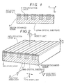
- a birefringence diffraction grating type polarizer in the embodiment according to the invention will now be explained with reference to Figures 1 and 2.
- a crystal substrate 1 having optical anisotropy is formed by a Y cut sheet of lithium niobate (LiNb03) in this embodiment.
- a series of proton exchanged regions 2 are provided regularly or periodically on the substrate 1.
- dielectric films 3 each having a refractive index equal to or substantially equal to that of the substrate 1, thereby providing an optical diffraction grating.
- Dielectric substances having such refractive indices are exemplified by lithium niobate (LiNb03), niobium pentoxide (N205), zirconium dioxide (Zr02), zinc sulphide (ZnS), titanium dioxide (Ti02), cerium dioxide (Ce02), tantalium pentoxide (Ta205) and tellurium dioxide (Te02).
- An anti-reflection film 4 of a uniform thickness is provided on the substrate 1 and on the dielectric films 3.
- This anti-reflection film 4 consists of a material having a refractive index approximating to the square root of the refractive index of the substrate 1, and has a uniform thickness equal to a dimension obtained by a calculation in which a light wavelength is divided by a value four times the refractive index of the anti-reflection film 4.
- a material having such a refractive index is selected from, for instance, silicon dioxide (Si02), calcium fluoride (CaF2), aluminum fluoride (AlF3), lanthanum fluoride (LaF3), strontium fluoride (SrF2) and magnesium fluoride (MgF2).
- the anti-reflection film 4 having such a refractive index reduces the reflection factor between the substrate 1 and the air to "zero", preventing the reflection on portions without the dielectric layer 3.
- the reflection induced at the boundary between the substrate 1 and the dielectric layer 3 is reduced to be almost "zero” because their refractive indices are almost equal to each other, and the reflection between the dielectric film 3 and the air is reduced to be almost “zero” in the presence of the anti-reflection layer 4 which is provided between the substrate 1 and the air. Therefore, the reflections on the two different substances of the polarizer surface composed of the substrate 1 and the dielectric film 3 are prevented simultaneously by simply depositing the anti-reflection film 4 of a uniform thickness.
- This anti-reflection film 4 may be composed of multiple layers providing an equivalent phase shift.
- the refractive index of the anti-reflection film 4 may be nearly equal to the square root of the product between the refractive index of the external material and that of the substrate 1.
- incident light 10 of circular polarization is split as a zero order diffraction light beam 11 of a polarization along the x-axis, and plus and minus order diffraction light beams 12 and 13 of a polarization orthogonal to the polarization of the zero order light beam 11.
- the intensity of the zero order diffraction light beam 11 of this diffraction grating is given by the function: cos 2 [nT p +(n d -1)T d ]/ ⁇ where ⁇ represents a light wavelength, n represents the change in the refractive index caused by the proton exchange, T p represents the depth of the proton exchanged regions 2, n d represents the refractive index of the dielectric film 3, and t d represents the thickness of the dielectric film 3.
- the refractive index of the substrate 1 of lithium niobate is about 2.2, and the change in the refractive index in accordance with the proton exchange is about +0.10 for the extraordinary ray, and is about -0.04 for the ordinary ray.
- the depth of the proton ion-replacement regions 2 is about 4.6 ⁇ m, and the thickness of the dielectric films 3 is about 0.16 ⁇ m, where niobium pentoxide (Nb205) having a refractive index of about 2.2 is used for the dielectric layer 3, so that the intensity of the zero order diffraction light beam 11 of this grating can be "0" for the extraordinary ray, and "1" for the ordinary ray, whereby the grating functions as a polarizer. If the Si02 layer giving a refractive index of 1.45 is used as the anti-reflection layer 4, the thickness of the Si02 layer should be about 2200 ⁇ .
- the proton exchanged regions 2 of 4.6 ⁇ m in depth can be provided by immersing the lithium niobate substrate 1 in liquified benzoic acid, for example at 250°C for four and a half hours.
- the niobium oxide film 3 of about 0.16 ⁇ m in thickness can be provided by spattering from a Nb205 target, or by reactive spattering from a Nb target in oxygen environment.
- the Si02 layer 4 of 2200 ⁇ in thickness can be provided by ordinary spattering.
- the angle of diffraction is almost inversely proportional to the pitch of the diffraction grating.
- the pitch of the grating is determined so as to obtain an angle of diffraction greater than that required for separating the diffracted light from the non-diffracted light.
- the angle of diffraction is 0.74° for a pitch of 100 ⁇ m, and is 7.5° for a pitch of 10 ⁇ m, respectively, where the wavelength is 1.3 ⁇ m.
- the birefringence diffraction grating type polarizer illustrated has the advantages that it can be made small in size and can be of low material cost. Furthermore it can be fabricated by a relatively simple process.
- an anti-reflection layer of a single material having a uniform thickness on a substrate provided with a series of proton exchanged regions thereon, thereby simplifying the fabricating process thereof.
- the uniform thickness of the anti-reflection layer prevents the disturbance of the phase condition in the diffraction grating, so that a sheet type polarizing element with a high extinction ratio and a low insertion loss is readily obtained.
Abstract
Description
- This invention relates to a birefringence diffraction grating type polarizer. Such a polarizer may be useful for various optical instruments making use of a LASER diode.
- A polarizer element, particularly a polarizing beam splitter, is an element in which specifically polarized light is obtained by changing the direction of light propagation between polarized light beams perpendicular to each other. Such an element is used as a component for constructing an optical isolator or an optical circulator in a light source module for an optical fiber communication system, an optical head for an optical disc, and so on.
- A conventional polarizing beam splitter such as a Glan-Thompson prism or Rochon prism is an element in which a light path is split based on the difference between the refraction angles or the total reflection angles of two orthogonally polarized light components at the reflection plane of a crystal with large birefringence, or an element in which light is totally reflected or transmitted in accordance with the difference of refractive indices of polarized light in a multilayer dielectric film formed at the reflection plane of a total reflection prism consisting of an isotropic optical medium, such as glass.
- With such a conventional polarizer element, however, there is a disadvantage that the size is large because the configuration is a cube having a side as long as √2 times the diameter of a transmitting light beam. This is because the conventional polarizer element has a reflection boundary surface which is positioned to be at a slant relative to the light axis by at least 45 degrees. In more detail, where the conventional polarizer element is applied to an optical disc for recording and reproducing, the transmitting light beam is large in size so that the configuration is a cube having a side of 8 to 10 mm.
- Another type of known polarizer element is disclosed in "National conference record, 1982, Optical & Radio wave Electronics, the Institute of Electronics & Communication Engineers of Japan,
Part 2". This known polarizer element consists of a birefringent tapered plate of Rutile (Ti0₂) having a tapered angle of 4 degrees. When a parallel light beam is incident on the birefringent tapered plate on one side thereof, the parallel light beam is subject to different refractions as between the extraordinary ray component and the ordinary ray component, so that the two components are split on the other side of the birefringent tapered plate with a split angle of approximately 1 degree. - With the birefringent tapered plate, however, there is the disadvantage that the fabricating process is complicated because the cutting of a tapered configuration is difficult on a mass-production basis, and the polishing of a tapered surface is also difficult to be carried out. There is a further disadvantage that Rutile is expensive.
- According to the invention, a birefringence diffraction grating type polarizing comprises an optically anisotropic sheet crystal substrate having periodic ion-exchanged regions to provide an optical diffraction grating; dielectric layers provided over the ion-exchanged regions, and having a refractive index proximate or equal to that of the crystal substrate; and an anti-reflection layer of a uniform thickness provided over the whole surface of the crystal substrate and the dielectric layers.
- The invention will be explained in more detail by way of example in conjunction with the appended drawings, in which:-
- Figure 1 is a cross-sectional view showing a birefringence diffraction grating type polarizer in an embodiment of the invention, and
- Figure 2 is a perspective view of the polarizer of Figure 1.
- Before explaining a birefringence diffraction grating type polarizer embodying the invention, the principle of operation will be briefly explained.
- In a polarizer making use of the invention, the reflection between crystal substrate and dielectric film is negligible, because the dielectric film has a refractive index proximate to that of the crystal substrate as described above for a polarizer of the birefringence diffraction grating type. Therefore, the surface of the polarizer is optically to be equivalent to the surface of a single substance. Accordingly, an anti-reflection layer can be provided by simply depositing a conventional anti-reflection layer of a uniform thickness on the crystal substrate. This simplifies significantly the fabricating process for growing the anti-reflection layer. Moreover, the phase condition of the diffraction grating is free from disturbance, because the thickness of the anti-reflection layer is uniform, so that the decrease of extinction ratio and the increase of diffraction loss which usually result from the presence of an anti-reflection layer can be avoided.
- A birefringence diffraction grating type polarizer in the embodiment according to the invention will now be explained with reference to Figures 1 and 2. A crystal substrate 1 having optical anisotropy is formed by a Y cut sheet of lithium niobate (LiNb0₃) in this embodiment. A series of proton exchanged
regions 2 are provided regularly or periodically on the substrate 1. On these proton exchangedregions 2 are formeddielectric films 3 each having a refractive index equal to or substantially equal to that of the substrate 1, thereby providing an optical diffraction grating. Dielectric substances having such refractive indices are exemplified by lithium niobate (LiNb0₃), niobium pentoxide (N₂0₅), zirconium dioxide (Zr0₂), zinc sulphide (ZnS), titanium dioxide (Ti0₂), cerium dioxide (Ce0₂), tantalium pentoxide (Ta₂0₅) and tellurium dioxide (Te0₂). Ananti-reflection film 4 of a uniform thickness is provided on the substrate 1 and on thedielectric films 3. Thisanti-reflection film 4 consists of a material having a refractive index approximating to the square root of the refractive index of the substrate 1, and has a uniform thickness equal to a dimension obtained by a calculation in which a light wavelength is divided by a value four times the refractive index of theanti-reflection film 4. - A material having such a refractive index is selected from, for instance, silicon dioxide (Si0₂), calcium fluoride (CaF₂), aluminum fluoride (AlF₃), lanthanum fluoride (LaF₃), strontium fluoride (SrF₂) and magnesium fluoride (MgF₂). The
anti-reflection film 4 having such a refractive index reduces the reflection factor between the substrate 1 and the air to "zero", preventing the reflection on portions without thedielectric layer 3. Further, the reflection induced at the boundary between the substrate 1 and thedielectric layer 3 is reduced to be almost "zero" because their refractive indices are almost equal to each other, and the reflection between thedielectric film 3 and the air is reduced to be almost "zero" in the presence of theanti-reflection layer 4 which is provided between the substrate 1 and the air. Therefore, the reflections on the two different substances of the polarizer surface composed of the substrate 1 and thedielectric film 3 are prevented simultaneously by simply depositing theanti-reflection film 4 of a uniform thickness. Thisanti-reflection film 4 may be composed of multiple layers providing an equivalent phase shift. In the case where the surface of the grating is in contact with an external material other than the air, the refractive index of theanti-reflection film 4 may be nearly equal to the square root of the product between the refractive index of the external material and that of the substrate 1. - In Figure 2
incident light 10 of circular polarization is split as a zero order diffraction light beam 11 of a polarization along the x-axis, and plus and minus orderdiffraction light beams 12 and 13 of a polarization orthogonal to the polarization of the zero order light beam 11. - The intensity of the zero order diffraction light beam 11 of this diffraction grating is given by the function: cos ² [nTp+(nd-1)Td]/λ where λ represents a light wavelength, n represents the change in the refractive index caused by the proton exchange, Tp represents the depth of the proton exchanged
regions 2, nd represents the refractive index of thedielectric film 3, and td represents the thickness of thedielectric film 3. Assuming that the light wavelength is 1.3µm, then the refractive index of the substrate 1 of lithium niobate is about 2.2, and the change in the refractive index in accordance with the proton exchange is about +0.10 for the extraordinary ray, and is about -0.04 for the ordinary ray. Therefore, the depth of the proton ion-replacement regions 2 is about 4.6µm, and the thickness of thedielectric films 3 is about 0.16µm, where niobium pentoxide (Nb₂0₅) having a refractive index of about 2.2 is used for thedielectric layer 3, so that the intensity of the zero order diffraction light beam 11 of this grating can be "0" for the extraordinary ray, and "1" for the ordinary ray, whereby the grating functions as a polarizer. If the Si0₂ layer giving a refractive index of 1.45 is used as theanti-reflection layer 4, the thickness of the Si0₂ layer should be about 2200Å. - The proton exchanged
regions 2 of 4.6µm in depth can be provided by immersing the lithium niobate substrate 1 in liquified benzoic acid, for example at 250°C for four and a half hours. Theniobium oxide film 3 of about 0.16µm in thickness can be provided by spattering from a Nb₂0₅ target, or by reactive spattering from a Nb target in oxygen environment. TheSi0₂ layer 4 of 2200Å in thickness can be provided by ordinary spattering. - The angle of diffraction is almost inversely proportional to the pitch of the diffraction grating. Hence, the pitch of the grating is determined so as to obtain an angle of diffraction greater than that required for separating the diffracted light from the non-diffracted light. For instance, the angle of diffraction is 0.74° for a pitch of 100µm, and is 7.5° for a pitch of 10µm, respectively, where the wavelength is 1.3µm.
- In this way a polarizer which is thin and of a low price can be obtained, since it can be fabricated from a thin lithium niobate sheet crystal in a mass by batch process. Thus the birefringence diffraction grating type polarizer illustrated has the advantages that it can be made small in size and can be of low material cost. Furthermore it can be fabricated by a relatively simple process.
- As described above, it is seen that light reflection can be avoided simply by disposing an anti-reflection layer of a single material having a uniform thickness on a substrate provided with a series of proton exchanged regions thereon, thereby simplifying the fabricating process thereof. The uniform thickness of the anti-reflection layer prevents the disturbance of the phase condition in the diffraction grating, so that a sheet type polarizing element with a high extinction ratio and a low insertion loss is readily obtained.
- Although the invention has been described with respect to a specific embodiment for complete and clear disclosure, the appended claims are not thus limited to it but are to be construed as embodying all modification and alternative constructions that may occur to one skilled in the art which fairly fall within the basic teaching herein set forth.
Claims (5)
an optically anisotropic sheet crystal substrate (1) having periodic ion-exchanged regions (2) to provide an optical diffraction grating;
dielectric layers (3) provided over said ion-exchanged regions, and having a refractive index proximate or equal to that of said crystal substrate; and
an anti-reflection layer (4) of a uniform thickness provided over the whole surface of said crystal substrate and said dielectric layers.
Applications Claiming Priority (2)
| Application Number | Priority Date | Filing Date | Title |
|---|---|---|---|
| JP63164049A JP2703930B2 (en) | 1988-06-29 | 1988-06-29 | Birefringent diffraction grating polarizer |
| JP164049/88 | 1988-06-29 |
Publications (3)
| Publication Number | Publication Date |
|---|---|
| EP0349144A2 true EP0349144A2 (en) | 1990-01-03 |
| EP0349144A3 EP0349144A3 (en) | 1991-05-29 |
| EP0349144B1 EP0349144B1 (en) | 1994-09-07 |
Family
ID=15785825
Family Applications (1)
| Application Number | Title | Priority Date | Filing Date |
|---|---|---|---|
| EP89305943A Expired - Lifetime EP0349144B1 (en) | 1988-06-29 | 1989-06-13 | Birefringence diffraction grating type polarizer |
Country Status (4)
| Country | Link |
|---|---|
| US (1) | US4991937A (en) |
| EP (1) | EP0349144B1 (en) |
| JP (1) | JP2703930B2 (en) |
| DE (1) | DE68918012T2 (en) |
Cited By (10)
| Publication number | Priority date | Publication date | Assignee | Title |
|---|---|---|---|---|
| WO1992021046A1 (en) * | 1991-05-11 | 1992-11-26 | The Technology Partnership Limited | Light scattering device |
| EP0565381A2 (en) * | 1992-04-08 | 1993-10-13 | Matsushita Electric Industrial Co., Ltd. | Optical element and method of fabricating the same |
| EP0612068A2 (en) * | 1993-02-16 | 1994-08-24 | Nec Corporation | Optical head device and birefringent diffraction grating polarizer and polarizing hologram element used therein |
| EP0656549A2 (en) * | 1993-12-01 | 1995-06-07 | International Business Machines Corporation | Optical elements and method for fabricating the same |
| GB2293021A (en) * | 1994-09-09 | 1996-03-13 | Sharp Kk | Polarisation dependent refractive device |
| EP0921418A2 (en) * | 1997-12-03 | 1999-06-09 | Canon Kabushiki Kaisha | Diffractive optical element and optical system having the same |
| US5914811A (en) * | 1996-08-30 | 1999-06-22 | University Of Houston | Birefringent grating polarizing beam splitter |
| EP0653609B1 (en) * | 1993-11-12 | 2000-01-05 | Dr. Johannes Heidenhain GmbH | Length- or angle of rotation measuring device |
| EP1158317A1 (en) * | 2000-05-22 | 2001-11-28 | Carl Zeiss | Echelle grating and use of an echelle grating |
| EP1192486A1 (en) * | 1999-06-22 | 2002-04-03 | Moxtek | Broadband wire grid polarizer for the visible spectrum |
Families Citing this family (51)
| Publication number | Priority date | Publication date | Assignee | Title |
|---|---|---|---|---|
| US5272685A (en) * | 1989-12-22 | 1993-12-21 | Kabushiki Kaisha Toshiba | Optical system for an information processing apparatus |
| JPH04174404A (en) * | 1990-11-07 | 1992-06-22 | Pioneer Electron Corp | Polarized beam splitter |
| US5245471A (en) * | 1991-06-14 | 1993-09-14 | Tdk Corporation | Polarizers, polarizer-equipped optical elements, and method of manufacturing the same |
| JP2658818B2 (en) * | 1993-02-24 | 1997-09-30 | 日本電気株式会社 | Birefringent diffraction grating polarizer and optical head device |
| US5739952A (en) * | 1994-04-14 | 1998-04-14 | Kabushiki Kaisha Sankyo Seiki Seisakusho | Polarizing beam splitter and optical head assembly |
| US5475772A (en) * | 1994-06-02 | 1995-12-12 | Honeywell Inc. | Spatial filter for improving polarization extinction ratio in a proton exchange wave guide device |
| JP2850878B2 (en) * | 1996-09-06 | 1999-01-27 | 日本電気株式会社 | Polarizing beam splitter and method of manufacturing the same |
| US6072629A (en) | 1997-02-26 | 2000-06-06 | Reveo, Inc. | Polarizer devices and methods for making the same |
| JP3445120B2 (en) * | 1997-09-30 | 2003-09-08 | キヤノン株式会社 | Exposure apparatus and device manufacturing method |
| US5920663A (en) * | 1997-12-24 | 1999-07-06 | Lucent Technologies Inc. | Optical waveguide router with controlled transmission characteristics |
| JPH11242118A (en) * | 1998-02-25 | 1999-09-07 | Seiko Epson Corp | Polarized light separating element, polarization conversion element and projection type display device |
| US6108131A (en) * | 1998-05-14 | 2000-08-22 | Moxtek | Polarizer apparatus for producing a generally polarized beam of light |
| US6208463B1 (en) | 1998-05-14 | 2001-03-27 | Moxtek | Polarizer apparatus for producing a generally polarized beam of light |
| US6288840B1 (en) | 1999-06-22 | 2001-09-11 | Moxtek | Imbedded wire grid polarizer for the visible spectrum |
| US6666556B2 (en) | 1999-07-28 | 2003-12-23 | Moxtek, Inc | Image projection system with a polarizing beam splitter |
| US6447120B2 (en) | 1999-07-28 | 2002-09-10 | Moxtex | Image projection system with a polarizing beam splitter |
| US6234634B1 (en) | 1999-07-28 | 2001-05-22 | Moxtek | Image projection system with a polarizing beam splitter |
| US7306338B2 (en) * | 1999-07-28 | 2007-12-11 | Moxtek, Inc | Image projection system with a polarizing beam splitter |
| US6243199B1 (en) | 1999-09-07 | 2001-06-05 | Moxtek | Broad band wire grid polarizing beam splitter for use in the visible wavelength region |
| US7375887B2 (en) | 2001-03-27 | 2008-05-20 | Moxtek, Inc. | Method and apparatus for correcting a visible light beam using a wire-grid polarizer |
| US7061561B2 (en) * | 2002-01-07 | 2006-06-13 | Moxtek, Inc. | System for creating a patterned polarization compensator |
| US6909473B2 (en) * | 2002-01-07 | 2005-06-21 | Eastman Kodak Company | Display apparatus and method |
| JP4078527B2 (en) * | 2002-03-26 | 2008-04-23 | 日本電気株式会社 | Structure of antireflection film on one-dimensional photonic crystal and method for forming the same |
| US6785050B2 (en) | 2002-05-09 | 2004-08-31 | Moxtek, Inc. | Corrosion resistant wire-grid polarizer and method of fabrication |
| US7113335B2 (en) * | 2002-12-30 | 2006-09-26 | Sales Tasso R | Grid polarizer with suppressed reflectivity |
| US7961393B2 (en) | 2004-12-06 | 2011-06-14 | Moxtek, Inc. | Selectively absorptive wire-grid polarizer |
| US20080055549A1 (en) * | 2006-08-31 | 2008-03-06 | Perkins Raymond T | Projection Display with an Inorganic, Dielectric Grid Polarizer |
| US7570424B2 (en) | 2004-12-06 | 2009-08-04 | Moxtek, Inc. | Multilayer wire-grid polarizer |
| US20080055722A1 (en) * | 2006-08-31 | 2008-03-06 | Perkins Raymond T | Optical Polarization Beam Combiner/Splitter with an Inorganic, Dielectric Grid Polarizer |
| US20080055721A1 (en) * | 2006-08-31 | 2008-03-06 | Perkins Raymond T | Light Recycling System with an Inorganic, Dielectric Grid Polarizer |
| US7800823B2 (en) | 2004-12-06 | 2010-09-21 | Moxtek, Inc. | Polarization device to polarize and further control light |
| US7630133B2 (en) * | 2004-12-06 | 2009-12-08 | Moxtek, Inc. | Inorganic, dielectric, grid polarizer and non-zero order diffraction grating |
| US20080055720A1 (en) * | 2006-08-31 | 2008-03-06 | Perkins Raymond T | Optical Data Storage System with an Inorganic, Dielectric Grid Polarizer |
| JP2007328128A (en) * | 2006-06-08 | 2007-12-20 | Ricoh Opt Ind Co Ltd | Optical element and its manufacturing method |
| US20070297052A1 (en) * | 2006-06-26 | 2007-12-27 | Bin Wang | Cube wire-grid polarizing beam splitter |
| US20070296921A1 (en) * | 2006-06-26 | 2007-12-27 | Bin Wang | Projection display with a cube wire-grid polarizing beam splitter |
| US8755113B2 (en) | 2006-08-31 | 2014-06-17 | Moxtek, Inc. | Durable, inorganic, absorptive, ultra-violet, grid polarizer |
| US7789515B2 (en) | 2007-05-17 | 2010-09-07 | Moxtek, Inc. | Projection device with a folded optical path and wire-grid polarizer |
| US20080316599A1 (en) * | 2007-06-22 | 2008-12-25 | Bin Wang | Reflection-Repressed Wire-Grid Polarizer |
| US20100103517A1 (en) * | 2008-10-29 | 2010-04-29 | Mark Alan Davis | Segmented film deposition |
| CN101738668B (en) | 2008-11-19 | 2011-12-07 | 上海丽恒光微电子科技有限公司 | Polarizing cube and method of fabricating the same |
| US8248696B2 (en) | 2009-06-25 | 2012-08-21 | Moxtek, Inc. | Nano fractal diffuser |
| US8611007B2 (en) | 2010-09-21 | 2013-12-17 | Moxtek, Inc. | Fine pitch wire grid polarizer |
| US8913321B2 (en) | 2010-09-21 | 2014-12-16 | Moxtek, Inc. | Fine pitch grid polarizer |
| US8913320B2 (en) | 2011-05-17 | 2014-12-16 | Moxtek, Inc. | Wire grid polarizer with bordered sections |
| US8873144B2 (en) | 2011-05-17 | 2014-10-28 | Moxtek, Inc. | Wire grid polarizer with multiple functionality sections |
| DE102012101555B4 (en) * | 2012-02-27 | 2013-12-24 | Fraunhofer-Gesellschaft zur Förderung der angewandten Forschung e.V. | Diffraction grating and method for its production |
| US8922890B2 (en) | 2012-03-21 | 2014-12-30 | Moxtek, Inc. | Polarizer edge rib modification |
| CN103149621A (en) * | 2013-03-11 | 2013-06-12 | 中国科学院上海光学精密机械研究所 | Reflecting type phase delay piece |
| US9348076B2 (en) | 2013-10-24 | 2016-05-24 | Moxtek, Inc. | Polarizer with variable inter-wire distance |
| CN107356954A (en) * | 2017-06-26 | 2017-11-17 | 同济大学 | A kind of photonic crystal scintillation component to be lighted with directionality |
Citations (4)
| Publication number | Priority date | Publication date | Assignee | Title |
|---|---|---|---|---|
| EP0039125A2 (en) * | 1980-04-25 | 1981-11-04 | Optical Coating Laboratory, Inc. | Optical article and method |
| JPS60188911A (en) * | 1984-03-08 | 1985-09-26 | Canon Inc | Optical coupler |
| JPS6355501A (en) * | 1986-08-26 | 1988-03-10 | Nec Corp | Diffraction grating type polarizing plate |
| JPH01107206A (en) * | 1987-10-20 | 1989-04-25 | Nec Corp | Manufacture of diffraction grating type polarizing plate |
Family Cites Families (13)
| Publication number | Priority date | Publication date | Assignee | Title |
|---|---|---|---|---|
| JPS5588009A (en) * | 1978-12-26 | 1980-07-03 | Nippon Telegr & Teleph Corp <Ntt> | Double refractive polarizing prism |
| US4228449A (en) * | 1978-12-26 | 1980-10-14 | Hughes Aircraft Company | Semiconductor diode array liquid crystal device |
| DE3066595D1 (en) * | 1979-08-21 | 1984-03-22 | Matsushita Electric Ind Co Ltd | Semiconductor stripe filter |
| US4359260A (en) * | 1980-06-25 | 1982-11-16 | Bell Telephone Laboratories, Incorporated | Optical polarizer |
| US4609267A (en) * | 1980-12-22 | 1986-09-02 | Seiko Epson Corporation | Synthetic resin lens and antireflection coating |
| JPS5964802A (en) * | 1982-10-05 | 1984-04-12 | Nitto Electric Ind Co Ltd | Circular polarization plate |
| US4619501A (en) * | 1985-01-08 | 1986-10-28 | The United States Of America As Represented By The Secretary Of The Air Force | Charge isolation in a spatial light modulator |
| US4655554A (en) * | 1985-03-06 | 1987-04-07 | The United States Of America As Represented By The Secretary Of The Air Force | Spatial light modulator having a capacitively coupled photoconductor |
| US4842376A (en) * | 1985-07-25 | 1989-06-27 | Hughes Aircraft Company | Double-schottky diode liquid crystal light valve |
| US4881110A (en) * | 1985-07-25 | 1989-11-14 | Hughes Aircraft Company | Double-Schottky diode liquid crystal light valve |
| JPH0685002B2 (en) * | 1986-02-18 | 1994-10-26 | ミノルタ株式会社 | Anti-reflection film for plastic optical parts |
| JP2742683B2 (en) * | 1986-08-08 | 1998-04-22 | 東洋通信機株式会社 | Manufacturing method of transmission diffraction grating |
| US4826300A (en) * | 1987-07-30 | 1989-05-02 | Hughes Aircraft Company | Silicon-on-sapphire liquid crystal light valve and method |
-
1988
- 1988-06-29 JP JP63164049A patent/JP2703930B2/en not_active Expired - Lifetime
-
1989
- 1989-06-13 DE DE68918012T patent/DE68918012T2/en not_active Expired - Lifetime
- 1989-06-13 EP EP89305943A patent/EP0349144B1/en not_active Expired - Lifetime
- 1989-06-27 US US07/371,899 patent/US4991937A/en not_active Expired - Lifetime
Patent Citations (4)
| Publication number | Priority date | Publication date | Assignee | Title |
|---|---|---|---|---|
| EP0039125A2 (en) * | 1980-04-25 | 1981-11-04 | Optical Coating Laboratory, Inc. | Optical article and method |
| JPS60188911A (en) * | 1984-03-08 | 1985-09-26 | Canon Inc | Optical coupler |
| JPS6355501A (en) * | 1986-08-26 | 1988-03-10 | Nec Corp | Diffraction grating type polarizing plate |
| JPH01107206A (en) * | 1987-10-20 | 1989-04-25 | Nec Corp | Manufacture of diffraction grating type polarizing plate |
Non-Patent Citations (2)
| Title |
|---|
| PATENT ABSTRACTS OF JAPAN, vol. 10, no. 41 (P-429)[2098], 18th February 1986; & JP-A-60 188 911 (CANON K.K.) 26-09-1985 * |
| PATENT ABSTRACTS OF JAPAN, vol. 12, no. 276 (P-737)[3123], 30th July 1988; & JP-A-63 055 501 (NEC CORP.) 10-03-1988 * |
Cited By (21)
| Publication number | Priority date | Publication date | Assignee | Title |
|---|---|---|---|---|
| WO1992021046A1 (en) * | 1991-05-11 | 1992-11-26 | The Technology Partnership Limited | Light scattering device |
| EP0565381A2 (en) * | 1992-04-08 | 1993-10-13 | Matsushita Electric Industrial Co., Ltd. | Optical element and method of fabricating the same |
| EP0565381A3 (en) * | 1992-04-08 | 1993-12-01 | Matsushita Electric Ind Co Ltd | Optical element and method of fabricating the same |
| US5367403A (en) * | 1992-04-08 | 1994-11-22 | Matsushita Electric Industrial Co., Ltd. | Optical element and method of fabricating the same |
| US5455712A (en) * | 1992-04-08 | 1995-10-03 | Matsushita Electric Industrial Co., Ltd. | Optical element and method of fabricating the same |
| EP0911822A2 (en) * | 1993-02-16 | 1999-04-28 | Nec Corporation | Optical head device and birefringent diffraction grating polarizer and polarizing hologram element used therein |
| EP0612068A2 (en) * | 1993-02-16 | 1994-08-24 | Nec Corporation | Optical head device and birefringent diffraction grating polarizer and polarizing hologram element used therein |
| EP0612068A3 (en) * | 1993-02-16 | 1995-12-06 | Nec Corp | Optical head device and birefringent diffraction grating polarizer and polarizing hologram element used therein. |
| EP0911822A3 (en) * | 1993-02-16 | 2004-09-22 | Nec Corporation | Optical head device and birefringent diffraction grating polarizer and polarizing hologram element used therein |
| EP0653609B1 (en) * | 1993-11-12 | 2000-01-05 | Dr. Johannes Heidenhain GmbH | Length- or angle of rotation measuring device |
| EP0656549A2 (en) * | 1993-12-01 | 1995-06-07 | International Business Machines Corporation | Optical elements and method for fabricating the same |
| EP0656549A3 (en) * | 1993-12-01 | 1996-01-17 | Ibm | Optical elements and method for fabricating the same. |
| US5671034A (en) * | 1994-09-09 | 1997-09-23 | Sharp Kabushiki Kaisha | Polarisation dependent refractive device exhibiting independtly varying first and second indices of refraction and methods of manufacture thereof |
| GB2293021A (en) * | 1994-09-09 | 1996-03-13 | Sharp Kk | Polarisation dependent refractive device |
| US5914811A (en) * | 1996-08-30 | 1999-06-22 | University Of Houston | Birefringent grating polarizing beam splitter |
| EP0921418A2 (en) * | 1997-12-03 | 1999-06-09 | Canon Kabushiki Kaisha | Diffractive optical element and optical system having the same |
| EP0921418A3 (en) * | 1997-12-03 | 1999-06-30 | Canon Kabushiki Kaisha | Diffractive optical element and optical system having the same |
| EP1192486A1 (en) * | 1999-06-22 | 2002-04-03 | Moxtek | Broadband wire grid polarizer for the visible spectrum |
| EP1192486A4 (en) * | 1999-06-22 | 2006-04-12 | Moxtek | Broadband wire grid polarizer for the visible spectrum |
| EP1158317A1 (en) * | 2000-05-22 | 2001-11-28 | Carl Zeiss | Echelle grating and use of an echelle grating |
| US6788465B2 (en) | 2000-05-22 | 2004-09-07 | Carl-Zeiss-Stiftung | Littrow grating and use of a littrow grating |
Also Published As
| Publication number | Publication date |
|---|---|
| US4991937A (en) | 1991-02-12 |
| DE68918012D1 (en) | 1994-10-13 |
| EP0349144A3 (en) | 1991-05-29 |
| DE68918012T2 (en) | 1995-03-30 |
| JP2703930B2 (en) | 1998-01-26 |
| EP0349144B1 (en) | 1994-09-07 |
| JPH0212106A (en) | 1990-01-17 |
Similar Documents
| Publication | Publication Date | Title |
|---|---|---|
| EP0349144B1 (en) | Birefringence diffraction grating type polarizer | |
| EP0349309B1 (en) | Birefringence diffraction grating type polarizer | |
| EP1420275B1 (en) | Isolator and optical attenuator | |
| EP0911822B1 (en) | Optical head device and birefringent diffraction grating polarizer and polarizing hologram element used therein | |
| US4492436A (en) | Polarization independent beam splitter | |
| US6018418A (en) | Polarization beam splitter | |
| US7012747B2 (en) | Polarizing beam splitter and polarizer using the same | |
| EP0307094B1 (en) | Optical image rotators | |
| KR920010621B1 (en) | Optical base material and optical product using the same and method of manufacturing the optical base material | |
| AU611739B2 (en) | Optical isolator | |
| JPS63314502A (en) | Double refractive diffraction grating type polarizing plate | |
| EP0488211A2 (en) | Polarization independent optical device | |
| JP2803181B2 (en) | Birefringent diffraction grating polarizer | |
| JPS63262602A (en) | Diffraction grating type optical polarizing plat | |
| JP2718112B2 (en) | Birefringent diffraction grating polarizer and method of manufacturing the same | |
| JPH0139561B2 (en) | ||
| JP3038942B2 (en) | Birefringent diffraction grating polarizer and optical isolator | |
| JP2710809B2 (en) | Crossed diffraction grating and polarization rotation detector using the same | |
| JP2658818B2 (en) | Birefringent diffraction grating polarizer and optical head device | |
| JPS6355501A (en) | Diffraction grating type polarizing plate | |
| JPH0830767B2 (en) | Hologram element | |
| JPH05196813A (en) | Diffraction grating type optical polarizing element | |
| JPH0827410B2 (en) | Polarizing prism | |
| JP2561912B2 (en) | Polarization separation waveguide | |
| JPH0212107A (en) | Birefringent diffraction grating type polarizer |
Legal Events
| Date | Code | Title | Description |
|---|---|---|---|
| PUAI | Public reference made under article 153(3) epc to a published international application that has entered the european phase |
Free format text: ORIGINAL CODE: 0009012 |
|
| 17P | Request for examination filed |
Effective date: 19890704 |
|
| AK | Designated contracting states |
Kind code of ref document: A2 Designated state(s): DE FR GB |
|
| PUAL | Search report despatched |
Free format text: ORIGINAL CODE: 0009013 |
|
| AK | Designated contracting states |
Kind code of ref document: A3 Designated state(s): DE FR GB |
|
| 17Q | First examination report despatched |
Effective date: 19930426 |
|
| GRAA | (expected) grant |
Free format text: ORIGINAL CODE: 0009210 |
|
| AK | Designated contracting states |
Kind code of ref document: B1 Designated state(s): DE FR GB |
|
| REF | Corresponds to: |
Ref document number: 68918012 Country of ref document: DE Date of ref document: 19941013 |
|
| ET | Fr: translation filed | ||
| PLBE | No opposition filed within time limit |
Free format text: ORIGINAL CODE: 0009261 |
|
| STAA | Information on the status of an ep patent application or granted ep patent |
Free format text: STATUS: NO OPPOSITION FILED WITHIN TIME LIMIT |
|
| 26N | No opposition filed | ||
| REG | Reference to a national code |
Ref country code: GB Ref legal event code: IF02 |
|
| PGFP | Annual fee paid to national office [announced via postgrant information from national office to epo] |
Ref country code: DE Payment date: 20080619 Year of fee payment: 20 |
|
| PGFP | Annual fee paid to national office [announced via postgrant information from national office to epo] |
Ref country code: FR Payment date: 20080617 Year of fee payment: 20 |
|
| PGFP | Annual fee paid to national office [announced via postgrant information from national office to epo] |
Ref country code: GB Payment date: 20080618 Year of fee payment: 20 |
|
| REG | Reference to a national code |
Ref country code: GB Ref legal event code: PE20 Expiry date: 20090612 |
|
| PG25 | Lapsed in a contracting state [announced via postgrant information from national office to epo] |
Ref country code: GB Free format text: LAPSE BECAUSE OF EXPIRATION OF PROTECTION Effective date: 20090612 |