EP0348122B1 - Optical data recording medium and manufacturing method thereof - Google Patents
Optical data recording medium and manufacturing method thereof Download PDFInfo
- Publication number
- EP0348122B1 EP0348122B1 EP19890306168 EP89306168A EP0348122B1 EP 0348122 B1 EP0348122 B1 EP 0348122B1 EP 19890306168 EP19890306168 EP 19890306168 EP 89306168 A EP89306168 A EP 89306168A EP 0348122 B1 EP0348122 B1 EP 0348122B1
- Authority
- EP
- European Patent Office
- Prior art keywords
- layer
- recording
- recording layer
- optical data
- recording medium
- Prior art date
- Legal status (The legal status is an assumption and is not a legal conclusion. Google has not performed a legal analysis and makes no representation as to the accuracy of the status listed.)
- Expired - Lifetime
Links
Images


Classifications
-
- G—PHYSICS
- G11—INFORMATION STORAGE
- G11B—INFORMATION STORAGE BASED ON RELATIVE MOVEMENT BETWEEN RECORD CARRIER AND TRANSDUCER
- G11B7/00—Recording or reproducing by optical means, e.g. recording using a thermal beam of optical radiation by modifying optical properties or the physical structure, reproducing using an optical beam at lower power by sensing optical properties; Record carriers therefor
- G11B7/24—Record carriers characterised by shape, structure or physical properties, or by the selection of the material
- G11B7/241—Record carriers characterised by shape, structure or physical properties, or by the selection of the material characterised by the selection of the material
- G11B7/252—Record carriers characterised by shape, structure or physical properties, or by the selection of the material characterised by the selection of the material of layers other than recording layers
- G11B7/257—Record carriers characterised by shape, structure or physical properties, or by the selection of the material characterised by the selection of the material of layers other than recording layers of layers having properties involved in recording or reproduction, e.g. optical interference layers or sensitising layers or dielectric layers, which are protecting the recording layers
- G11B7/2572—Record carriers characterised by shape, structure or physical properties, or by the selection of the material characterised by the selection of the material of layers other than recording layers of layers having properties involved in recording or reproduction, e.g. optical interference layers or sensitising layers or dielectric layers, which are protecting the recording layers consisting essentially of organic materials
- G11B7/2575—Record carriers characterised by shape, structure or physical properties, or by the selection of the material characterised by the selection of the material of layers other than recording layers of layers having properties involved in recording or reproduction, e.g. optical interference layers or sensitising layers or dielectric layers, which are protecting the recording layers consisting essentially of organic materials resins
-
- G—PHYSICS
- G11—INFORMATION STORAGE
- G11B—INFORMATION STORAGE BASED ON RELATIVE MOVEMENT BETWEEN RECORD CARRIER AND TRANSDUCER
- G11B7/00—Recording or reproducing by optical means, e.g. recording using a thermal beam of optical radiation by modifying optical properties or the physical structure, reproducing using an optical beam at lower power by sensing optical properties; Record carriers therefor
- G11B7/24—Record carriers characterised by shape, structure or physical properties, or by the selection of the material
- G11B7/241—Record carriers characterised by shape, structure or physical properties, or by the selection of the material characterised by the selection of the material
- G11B7/242—Record carriers characterised by shape, structure or physical properties, or by the selection of the material characterised by the selection of the material of recording layers
- G11B7/244—Record carriers characterised by shape, structure or physical properties, or by the selection of the material characterised by the selection of the material of recording layers comprising organic materials only
- G11B7/246—Record carriers characterised by shape, structure or physical properties, or by the selection of the material characterised by the selection of the material of recording layers comprising organic materials only containing dyes
- G11B7/247—Record carriers characterised by shape, structure or physical properties, or by the selection of the material characterised by the selection of the material of recording layers comprising organic materials only containing dyes methine or polymethine dyes
- G11B7/2472—Record carriers characterised by shape, structure or physical properties, or by the selection of the material characterised by the selection of the material of recording layers comprising organic materials only containing dyes methine or polymethine dyes cyanine
-
- G—PHYSICS
- G11—INFORMATION STORAGE
- G11B—INFORMATION STORAGE BASED ON RELATIVE MOVEMENT BETWEEN RECORD CARRIER AND TRANSDUCER
- G11B7/00—Recording or reproducing by optical means, e.g. recording using a thermal beam of optical radiation by modifying optical properties or the physical structure, reproducing using an optical beam at lower power by sensing optical properties; Record carriers therefor
- G11B7/24—Record carriers characterised by shape, structure or physical properties, or by the selection of the material
- G11B7/241—Record carriers characterised by shape, structure or physical properties, or by the selection of the material characterised by the selection of the material
- G11B7/242—Record carriers characterised by shape, structure or physical properties, or by the selection of the material characterised by the selection of the material of recording layers
- G11B7/244—Record carriers characterised by shape, structure or physical properties, or by the selection of the material characterised by the selection of the material of recording layers comprising organic materials only
- G11B7/246—Record carriers characterised by shape, structure or physical properties, or by the selection of the material characterised by the selection of the material of recording layers comprising organic materials only containing dyes
- G11B7/2463—Record carriers characterised by shape, structure or physical properties, or by the selection of the material characterised by the selection of the material of recording layers comprising organic materials only containing dyes azulene
-
- G—PHYSICS
- G11—INFORMATION STORAGE
- G11B—INFORMATION STORAGE BASED ON RELATIVE MOVEMENT BETWEEN RECORD CARRIER AND TRANSDUCER
- G11B7/00—Recording or reproducing by optical means, e.g. recording using a thermal beam of optical radiation by modifying optical properties or the physical structure, reproducing using an optical beam at lower power by sensing optical properties; Record carriers therefor
- G11B7/24—Record carriers characterised by shape, structure or physical properties, or by the selection of the material
- G11B7/241—Record carriers characterised by shape, structure or physical properties, or by the selection of the material characterised by the selection of the material
- G11B7/242—Record carriers characterised by shape, structure or physical properties, or by the selection of the material characterised by the selection of the material of recording layers
- G11B7/244—Record carriers characterised by shape, structure or physical properties, or by the selection of the material characterised by the selection of the material of recording layers comprising organic materials only
- G11B7/246—Record carriers characterised by shape, structure or physical properties, or by the selection of the material characterised by the selection of the material of recording layers comprising organic materials only containing dyes
- G11B7/2467—Record carriers characterised by shape, structure or physical properties, or by the selection of the material characterised by the selection of the material of recording layers comprising organic materials only containing dyes azo-dyes
-
- G—PHYSICS
- G11—INFORMATION STORAGE
- G11B—INFORMATION STORAGE BASED ON RELATIVE MOVEMENT BETWEEN RECORD CARRIER AND TRANSDUCER
- G11B7/00—Recording or reproducing by optical means, e.g. recording using a thermal beam of optical radiation by modifying optical properties or the physical structure, reproducing using an optical beam at lower power by sensing optical properties; Record carriers therefor
- G11B7/24—Record carriers characterised by shape, structure or physical properties, or by the selection of the material
- G11B7/241—Record carriers characterised by shape, structure or physical properties, or by the selection of the material characterised by the selection of the material
- G11B7/242—Record carriers characterised by shape, structure or physical properties, or by the selection of the material characterised by the selection of the material of recording layers
- G11B7/244—Record carriers characterised by shape, structure or physical properties, or by the selection of the material characterised by the selection of the material of recording layers comprising organic materials only
- G11B7/246—Record carriers characterised by shape, structure or physical properties, or by the selection of the material characterised by the selection of the material of recording layers comprising organic materials only containing dyes
- G11B7/248—Record carriers characterised by shape, structure or physical properties, or by the selection of the material characterised by the selection of the material of recording layers comprising organic materials only containing dyes porphines; azaporphines, e.g. phthalocyanines
-
- G—PHYSICS
- G11—INFORMATION STORAGE
- G11B—INFORMATION STORAGE BASED ON RELATIVE MOVEMENT BETWEEN RECORD CARRIER AND TRANSDUCER
- G11B7/00—Recording or reproducing by optical means, e.g. recording using a thermal beam of optical radiation by modifying optical properties or the physical structure, reproducing using an optical beam at lower power by sensing optical properties; Record carriers therefor
- G11B7/24—Record carriers characterised by shape, structure or physical properties, or by the selection of the material
- G11B7/241—Record carriers characterised by shape, structure or physical properties, or by the selection of the material characterised by the selection of the material
- G11B7/242—Record carriers characterised by shape, structure or physical properties, or by the selection of the material characterised by the selection of the material of recording layers
- G11B7/244—Record carriers characterised by shape, structure or physical properties, or by the selection of the material characterised by the selection of the material of recording layers comprising organic materials only
- G11B7/249—Record carriers characterised by shape, structure or physical properties, or by the selection of the material characterised by the selection of the material of recording layers comprising organic materials only containing organometallic compounds
-
- G—PHYSICS
- G11—INFORMATION STORAGE
- G11B—INFORMATION STORAGE BASED ON RELATIVE MOVEMENT BETWEEN RECORD CARRIER AND TRANSDUCER
- G11B7/00—Recording or reproducing by optical means, e.g. recording using a thermal beam of optical radiation by modifying optical properties or the physical structure, reproducing using an optical beam at lower power by sensing optical properties; Record carriers therefor
- G11B7/24—Record carriers characterised by shape, structure or physical properties, or by the selection of the material
- G11B7/241—Record carriers characterised by shape, structure or physical properties, or by the selection of the material characterised by the selection of the material
- G11B7/252—Record carriers characterised by shape, structure or physical properties, or by the selection of the material characterised by the selection of the material of layers other than recording layers
- G11B7/253—Record carriers characterised by shape, structure or physical properties, or by the selection of the material characterised by the selection of the material of layers other than recording layers of substrates
- G11B7/2533—Record carriers characterised by shape, structure or physical properties, or by the selection of the material characterised by the selection of the material of layers other than recording layers of substrates comprising resins
- G11B7/2534—Record carriers characterised by shape, structure or physical properties, or by the selection of the material characterised by the selection of the material of layers other than recording layers of substrates comprising resins polycarbonates [PC]
-
- G—PHYSICS
- G11—INFORMATION STORAGE
- G11B—INFORMATION STORAGE BASED ON RELATIVE MOVEMENT BETWEEN RECORD CARRIER AND TRANSDUCER
- G11B7/00—Recording or reproducing by optical means, e.g. recording using a thermal beam of optical radiation by modifying optical properties or the physical structure, reproducing using an optical beam at lower power by sensing optical properties; Record carriers therefor
- G11B7/24—Record carriers characterised by shape, structure or physical properties, or by the selection of the material
- G11B7/241—Record carriers characterised by shape, structure or physical properties, or by the selection of the material characterised by the selection of the material
- G11B7/252—Record carriers characterised by shape, structure or physical properties, or by the selection of the material characterised by the selection of the material of layers other than recording layers
- G11B7/254—Record carriers characterised by shape, structure or physical properties, or by the selection of the material characterised by the selection of the material of layers other than recording layers of protective topcoat layers
- G11B7/2542—Record carriers characterised by shape, structure or physical properties, or by the selection of the material characterised by the selection of the material of layers other than recording layers of protective topcoat layers consisting essentially of organic resins
-
- Y—GENERAL TAGGING OF NEW TECHNOLOGICAL DEVELOPMENTS; GENERAL TAGGING OF CROSS-SECTIONAL TECHNOLOGIES SPANNING OVER SEVERAL SECTIONS OF THE IPC; TECHNICAL SUBJECTS COVERED BY FORMER USPC CROSS-REFERENCE ART COLLECTIONS [XRACs] AND DIGESTS
- Y10—TECHNICAL SUBJECTS COVERED BY FORMER USPC
- Y10S—TECHNICAL SUBJECTS COVERED BY FORMER USPC CROSS-REFERENCE ART COLLECTIONS [XRACs] AND DIGESTS
- Y10S428/00—Stock material or miscellaneous articles
- Y10S428/913—Material designed to be responsive to temperature, light, moisture
-
- Y—GENERAL TAGGING OF NEW TECHNOLOGICAL DEVELOPMENTS; GENERAL TAGGING OF CROSS-SECTIONAL TECHNOLOGIES SPANNING OVER SEVERAL SECTIONS OF THE IPC; TECHNICAL SUBJECTS COVERED BY FORMER USPC CROSS-REFERENCE ART COLLECTIONS [XRACs] AND DIGESTS
- Y10—TECHNICAL SUBJECTS COVERED BY FORMER USPC
- Y10T—TECHNICAL SUBJECTS COVERED BY FORMER US CLASSIFICATION
- Y10T428/00—Stock material or miscellaneous articles
- Y10T428/31504—Composite [nonstructural laminate]
- Y10T428/31507—Of polycarbonate
-
- Y—GENERAL TAGGING OF NEW TECHNOLOGICAL DEVELOPMENTS; GENERAL TAGGING OF CROSS-SECTIONAL TECHNOLOGIES SPANNING OVER SEVERAL SECTIONS OF THE IPC; TECHNICAL SUBJECTS COVERED BY FORMER USPC CROSS-REFERENCE ART COLLECTIONS [XRACs] AND DIGESTS
- Y10—TECHNICAL SUBJECTS COVERED BY FORMER USPC
- Y10T—TECHNICAL SUBJECTS COVERED BY FORMER US CLASSIFICATION
- Y10T428/00—Stock material or miscellaneous articles
- Y10T428/31504—Composite [nonstructural laminate]
- Y10T428/31855—Of addition polymer from unsaturated monomers
- Y10T428/31935—Ester, halide or nitrile of addition polymer
Definitions
- the present invention relates to an optical data recording medium such as an optical disk and a manufacturing method for this medium, and more specifically, to an optical data recording medium suitably used in a WO (write once) type optical disk provided, for example, with a recording layer composed of an organic dye type heat mode recording material and a manufacturing method for this medium.
- WO write once
- CDs compact disks
- DRAW direct read after write
- a metal material such as Te for ablation type medium or a metal material such as In for a so-called phase changing type medium effecting dislocation from crystal to non-crystal is considered to be useful as a void type optical recording material having the DRAW function. Since, however, a recording layer composed of these metal type recording materials is formed using a thin film formation technique such as a vapor-deposition method or a sputtering method, there remains a problem in mass-productivity and cost.
- a pit type (heat mode WO type) organic dye type recording material which can be formed to a film by a spin coating method is considered more viable with respect to productivity.
- An optical disk in particular, an optical disk using organic dye as a recording material must be provided with a protective layer for protecting a recording layer, and this protective layer is preferably formed by a spin coating method in consideration of for example manufacturing costs and mass productivity. Then, in general, a CD is provided with a protective layer composed of, e.g., an acrylate resin formed by a spin coating method.
- optical data recording medium which comprises a transparent substrate composed of a polymethyl methacrylate resin or glass having a thin film of a dye such as squarylium, thiopyrylium formed thereon and pits formed on the thin film by irradiation of a laser beam.
- a dye such as squarylium, thiopyrylium formed thereon and pits formed on the thin film by irradiation of a laser beam.
- a reflecting layer is formed on a plastic film in a flattened layer
- a recording layer composed of a mixture of dye and polymer is formed on the reflecting layer and recording pits are defined by irradiation of a laser beam
- a recording layer composed of a mixture of dye and styrene oligomer is formed (A. Kuroiwa et al., Jap. J. Appl. Phys. 22, 340, 1983), and on all of which data are recorded by formation of pits.
- a recording layer is composed of a single dye of these various organic dyes
- the dye remains on the bottom portions of pits defined by irradiation of a laser beam and the laser beam irradiated at the portion where the dye remains is reflected. Therefore, there is no difference between reflection factors at a flat portion and that at a pit portion, and thus a sufficient modulation factor cannot be obtained. Further, since the pits have a rim portion of the edges thereof shaped to a gentle and obscure configuration, this recording medium has a problem in that a signal output does not rise sharply.
- the recording medium provided with the recording layer composed of the mixture of the dye and polymer or the mixture of the dye and styrene oligomer has lower light absorption and light reflection than those of the recording layers composed of the single dye, and then has a lower modulation factor. Further, not only this recording medium requires a larger power when a laser beam is irradiated thereon but also the configuration of the pits thereof is not clearly defined like the recording medium using the single dye so that the medium has a problem in recording reliability.
- the recording layer when a recording layer is formed on a transparent substrate and a laser beam is irradiated thereon, the recording layer is heat-melted at the portion where the beam is irradiated and the thickness of the recording layer is made thinner or the substrate is exposed at this portion.
- a signal can be read out because a reflection factor of the portion is lowered. Since, however, the difference between the reflection factors at a non-recorded portion and that at a recorded portion is small, a sufficient modulation factor cannot be obtained and reproduction errors are caused.
- a metal film is expanded by a vapor pressure produced by partially heating an organic film by the irradiation of a laser beam thereby to form bubbles for recording data.
- this method reproduces a signal by making use of reflection effected on a surface of a metal film and this metal film is formed by a thin film formation technique such as a vapor-deposition method or a sputtering method, there remains a problem in mass-productivity and cost.
- the dye is usually unstable under high light conditions, in particular under sunlight, and thus this recording medium has a drawback that the dye is observed to be degraded.
- said protective layer is formed on the recording layer by applying a water solution of a water-soluble polymer to the recording layer to be dried.
- an optical data recording medium comprising a transparent substrate, a recording layer formed on the substrate and a thin layer, 10 nm to 400 ⁇ m thick, formed on the recording layer, characterized in that the recording layer has a refraction factor higher than that of the substrate, and that the recording layer on exposure to light or heat caused by irradiation with light is capable of forming voids within the recording layer, or between the recording layer and the substrate. Additionally voids may be formed between the thin layer and the substrate.
- the optical data recording medium according to the invention has a high modulation factor capable of being produced at low cost. Further the presence of the thin layer over the recording layer provides protection for the recording layer.
- the optical data recording medium according to the present invention is characterized by having voids for signals defined in the recording layer or between the recording layer and the substrate.
- the thin layer may be substantially deformed to the opposite side of the substrate by heating the recording layer by a radiation beam irradiated from the substrate side or the side opposite to the substrate.
- the recording layer of the optical data recording medium according to the invention may suitably be composed of an organic dye type recording material, preferably of a cyanine type dye.
- the recording layer of the optical data recording medium may suitably be composed of an organic dye type recording medium and fibre-shaped connections are defined in the voids.
- the thin layer of the optical data recording medium according to the invention is suitably composed of a hydrophilic polymer, preferably of a cross-linked polyvinyl alcohol.
- the recording layer is capable of recording data through melting, expansion, decomposition, or sublimation and contains a cyanine dye which starts to be melted at a temperature of 100°C or more and within a range of a laser beam power of 10 mW or less and an infrared ray absorbing agent of 20 wt % or less with respect to the cyanine dye, which exhibits absorption in a wavelength region longer than that of the maximum absorption peak of the cyanine dye; and the thin layer is composed of a hydrophilic resin subjected to a heat treatment or a radiation beam irradiation treatment.
- This embodiment provides an optical data recording medium having a high recording sensitivity and resistance to high light condition.
- one of the recording layer and the thin layer is formed from a sparingly water-dispersible component the other is formed from a water-dispersible component.
- a protective layer which may be capable of being formed on a recording layer composed of an organic dye type recording material by a spin coating method and can reduce costs of an optical disk having the above DRAW function.
- the optical data recording medium according to the invention also comprises an overcoat layer composed of an acrylate resin formed on the thin layer.
- the optical data recording medium according to the invention suitably has a total thickness of 1.1 to 1.5 mm.
- the said method is characterized in that the above recording layer is composed of a material which is "neither easily dissolved nor easily dispersed in water" (referred to as "a difficult-to-dissolve-in-water property", hereinafter) and the above thin layer is composed of hydrophilic polymer, and the thin layer is subjected to a water-proofing treatment by a polymerization reaction.
- an optical data recording medium which comprises a transparent substrate and a recording layer and a thin layer formed on the transparent substrate characterized by forming the recording layer from a material slightly soluble in the aqueous solution used for application of the thin layer under the application conditions used; and forming the thin layer from an aqueous solution of protective film material by direct application onto the recording layer followed by drying.
- the recording layer may be formed from a material dissolved in non-aqueous solvent by direct application onto the substrate, followed by drying.
- the direct application method employed may be spin coating.
- one of the recording layer component and the thin layer component is formed from a water-insoluble material and the other is formed from a water-soluble material, both being formed by spin coating, followed by drying.
- an optical data recording medium in write once recording wherein the recording layer is exposed to light or to heat caused by irradiation with light such that voids are formed within the recording layer or between the recording layer and the substrate.
- a process for write once recording on an optical data recording medium comprises exposing the recording layer of the optical data recording medium to light or to heat caused by irradiation with light such that voids are formed within the recording layer or between the recording layer and the substrate.
- the material used as the component of the recording layer in this invention is an organic dye material which is difficult to disperse and dissolve in water, very difficult to react with water, and little wettable to water.
- a material used for the thin, protective layer is a polymer such as polyvinylalcohol; which is water soluble, shows surface activity to said organic dye of recording layer in a coated water solution in a protective layer, to be wettable to said organic dye or recording layer.
- the thin layer used according to the invention composed of the above hydrophilic polymer can be formed by a spin coating method of high productivity without affecting the recording layer when the recording layer is composed of the organic dye type recording material which has a difficult-to-dissolve-in-water property. It is enough to be insoluble in water for a few seconds while the spin coating is being effected to laminate the hydrophilic polymer to be difficult to be dissolved in water for the recording layer mentioned above. Hence it is acceptable that the recording layer has a slight water solubility.
- this thin layer is hydrophilic and has low solubility to an organic solvent
- a UV curing type resin such as an acrylate resin can be formed on the thin layer as an overcoat layer without affecting the thin layer even if by a spin coating method, and this overcoat layer can also be formed by a spin coating method.
- voids for signals are defined within the recording layer or between the recording layer and the substrate so that the modulation factor is increased by using an optical interference effect described in detail later thereby to provide highly reliable optical data recording medium.
- the method of manufacturing an optical data recording medium using an organic dye compound as a material for the recording layer and where the recording layer is formed by applying the compound to the transparent substrate by spin coating can be operated at a low cost with improved productivity.
- Decomposition, sublimation and heat-melting must be effected in a low temperature range to form clear voids by an irradiation of a laser beam to the recording layer.
- a dye which is thermally unstable at a temperature of 230°C or less is preferably used, while when a dye which is thermally unstable at a temperature of 230°C or higher is used, the recording layer of high sensitivity cannot be obtained.
- the lower limit of the thermal instability is 100°C, which corresponds to a maximum temperature in a compartment of an automobile parking under the blazing sun in summer, and thus this temperature must be the lower limit temperature.
- the upper limit of 230°C is a temperature preferable to satisfy the recording conditions such as a light power of 10 mW or less, a linear velocity of 6 m/sec. or more and a light pulsewidth of about 100 n sec., and the light power exceeding 10 mW is inconvenient because of the increase in power consumption and also from a view point of the durability of a laser beam and costs.
- the light pulsewidth is related to the linear velocity, and a broader pulsewidth encountered with a higher linear velocity results in a lowered recording capacity. Therefore, the light pulsewidth is preferably about 100 n sec., although it has a relation to the linear velocity.
- a melting dye In order to form voids effectively in short time, a melting dye must not be expanded two-dimensionally but must be expanded three-dimensionally.
- a hydrophilic polymer is cross-linked on the recording layer or a thermally deformable layer subjected to a heat treatment is formed thereon so that it receives heat from the recording layer when a laser beam is irradiated and protrudes toward the opposite side with respect to the substrate thereby to expand the dye three-dimensionally.
- the pressure in the thermally deformable layer is increased simultaneously by the dissolution and sublimation of the dye and the formation of voids is accelerated by the increase in pressure.
- a material used as the thermally deformable layer must be water-proof and moisture resistant.
- the thermally deformable layer Since a cyanine dye or the like used is generally insoluble to water, the hydrophilic polymer used as a material of the thermally deformable layer does not damage the recording layer in lamination. Since, however, the thermally deformable layer is hydrophilic, it absorbs water in the air to be deformed and swelled. Therefore, the water-proof and moisture resistance of the thermally deformable layer is improved by, for example, a cross-link treatment by an addition of a cross-link agent, a heat treatment, a radiation treatment.
- the deterioration of the recording layer by a reproducing light beam includes a deterioration caused by heat of a laser beam and a deterioration caused by light.
- the thermal deterioration is restricted by providing a thermally deformable layer and transferring heat therethrough to it to reduce an accumulation of heat.
- the deterioration caused by light can be restricted by adding to the cyanine dye an infrared absorption agent which exhibits absorption in a wavelength region longer than water-proof and moisture resistant.
- the thermally deformable layer Since a cyanine dye used is generally insoluble to water, the hydrophilic polymer used as a material of the thermally deformable layer does not damage the recording layer in lamination. Since, however, the thermally deformable layer is hydrophilic, it absorbs water in the air to be deformed and swelled. Therefore, the water-proof and moisture resistance of the thermally deformable layer is for example improved by a cross-link treatment by an addition of a cross-link agent, a heat treatment, a radiation treatment.
- the deterioration of the recording layer by a reproducing light beam includes a deterioration caused by heat of a laser beam and a deterioration caused by light.
- the thermal deterioration is restricted by providing a thermally deformable layer and transferring heat therethrough to it to reduce an accumulation of heat.
- the deterioration caused by light can be restricted by adding to the cyanine dye an infrared absorption agent which exhibits absorption in a wavelength region longer than that in the maximum absorption peak of the cyanine dye, the cyanine dye being changed to a stable energy state.
- an infrared absorbing agent of 20 wt % or more is contained in the cyanine dye
- the stability of the cyanine dye adversely affects recording sensitivity, and that in the maximum absorption peak of the cyanine dye, the cyanine dye being changed to a stable energy state.
- an infrared absorbing agent of 20 wt % or more is contained in the cyanine dye, the stability of the cyanine dye adversely affects recording sensitivity, and sensitivity is lowered.
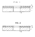
- Fig. 1 is a schematic partial and cross sectional view of an optical disk of the first embodiment, wherein 1 designates a transparent disk-shaped substrate, which may be of a transparent resin material such as polycarbonate, polymethyl methacrylate, polymethyl penten, epoxy resin or transparent ceramics such as glass, while in this embodiment a polycarbonate substrate is used. Note that la designates a center through hole of the substrate 1.
- a transparent resin material such as polycarbonate, polymethyl methacrylate, polymethyl penten, epoxy resin or transparent ceramics such as glass
- Designated at 2 is a recording layer formed on the substrate 1 by a spin coating method and composed of an organic dye type heat mode recording material difficult-to-dissolve-in-water.
- This organic dye type heat mode recording material may be composed, for example, of a polymethyne dye, an anthraquinone dye, a cyanine dye, a phthalocyanine dye, a xanthene dye, a tri-phenyl methane dye, a pyrilium dye, an azulene dye, a metals containing azo dye.
- This embodiment uses a cyanine dye type material, and a methanol solution containing the cyanine dye is applied to the substrate 1 by a spin coating method to form the recording layer 2.
- this recording layer 2 means that it is not dissolved in water for a few seconds while a spin coating of a thin layer composed of hydrophilic polymer described later is being effected and the recording layer 2 may be slightly dissolved in water.
- Designated at 3 is the thin layer composed of the hydrophilic polymer and formed on the recording layer 2 by a spin coating method, and this thin layer 3 may be composed of the following water-soluble resins.
- This embodiment uses the polyvinyl alcohol (PVA) as the thin layer 3, and a water solution containing the PVA is applied by a spin coating method to form the thin layer 3 having a film thickness of 120 nm.
- PVA polyvinyl alcohol
- the thin layer 3 must have the film thickness of 10 nm to 400 ⁇ m, preferably 60 nm (0.06 ⁇ m) or more. When the thickness is less than 60 nm, pin holes may be created and thus water and foreign matter penetrates through these pin holes and is deposited on the recording layer 2 and causes errors. In addition, when an overcoat layer is additionally formed on the thin layer 3, the overcoat material penetrates through these pin holes and attacks the recording layer 2. Therefore, the thin layer 3 preferably has the thickness of 60 nm or more.
- the upper limit thickness of the thin layer is limited to 400 ⁇ m or less because the CD standard specifies the thickness of a substrate to 1.2 ⁇ 0.1 mm and the total thickness of a disk to 1.2 +0.3 / -0.1 mm at present.
- the film thickness of the thin layer 3 can be adjusted by the selection of e.g. a rotational mode of the substrate 1, a dropping condition, concentration, the atmosphere around a turn table when the spin coating of the PVA is effected.
- the thin layer 3 is composed of the water-soluble polymer such as the PVA, its moisture resistance is lowered.
- the thin layer 3 is subjected to e.g. a cross-linking treatment to provide it with water-proof (moisture resistance) and heat resistance.
- a cross-linking agent or the like is added into a water solution of the water soluble polymer, and after the thin layer 3 is formed, cross-linking reaction is effected by irradiation of light or a cross-linking reaction is effected by heating.
- the thin layer 3 with no addition of the cross-linking agent is heated and crystallized (for example, since the PVA is used in this embodiment, the PVA is denaturated) or subjected to other treatments so that it is made insoluble to water, water-proof and heat resistant.
- this embodiment employs a technique wherein chrome is added as a cross-linking agent and the cross-linking reaction is effected in the thin layer 3 by the irradiation of light.
- cross-linking means examples are shown as follows and any arbitrary means can be employed as necessary.
- Designated at 4 is an overcoat layer formed on the thin layer 3 by a spin coating method, and in this embodiment, an acrylate resin as a UV curing type resin is used and its film thickness is selected to be 100 ⁇ m. Note that the overcoat 4 may be composed of a suitable material other than the acrylate resin.
- both the layers are irradiated by ultraviolet rays, the thin layer 3 is cross-linked and the overcoat layer 4 is polymerized to be provided with water-proof and heat resistance.
- a recorded void (pit) array had a length of 0.9 - 3.3 ⁇ m and intervals of 0.9 - 3.3 ⁇ m.
- a spin coating was effected on the substrate to form a recording layer of 80 nm thick using a methyl alcohol solution as cyanine dye containing 1.5 wt % of 1-methyl-2-[7-(1-methyl 2-indolinydene) 1,3,5-heptatrienyl] 3,3-dibutyl-indolium-hexafluorophosphate.
- a 10% water solution containing a mixture of polyvinyl alcohol having a degree of saponification of 88.0% and a degree of polymerization of 1700 and bichromate ammonium of 10% with respect to the polyvinyl alcohol was prepared.
- This solution was applied to the recording layer by a spin coating to form a thin layer of 60 nm thick. After this thin layer was dried, ultraviolet rays were irradiated thereto for 30 sec. from a position 15 cm apart therefrom with a power of 2.4 KW to form an air sandwich type optical disk using an organic dye by cross-linking the above polyvinyl alcohol.
- a water solution containing 15% of sodium 2-acrylamide-2-methyl propane-sulfonate polymer described in Japanese Patent Kokoku No. 1-14879 was prepared and applied to a dye recording layer to a thickness of 60 nm to form an air sandwich type optical disk.
- cross-linked polyvinyl alcohol having a softening point of 200°C or more is most preferably used as a thin layer material.
- the cross-linked polyvinyl alcohol has a softening point of 200 - 230°C.
- the cyanine dye used as a recording material in the present invention has the melting point or the decomposing temperature of 200 - 230°C, when a recording layer reaches this temperature by an irradiation of a laser beam, the dye layer is liquefied and vaporized to cause a thin layer where the laser beam is irradiated to be swelled, whereby a high C/N is obtained, and when the thin layer is formed by a material having a softening point of 200°C or more, the most preferable recording can be carried out.
- the thin layer is formed by a material having a softening point of 200°C or less such as the sodium-2-acrylamide-2-methylpropane-sulfonate polymer as described in Japanese Patent Kokoku No. 1-14879, a portion where the laser beam is irradiated melts even the thin layer together with the dye layer and defines holes, resulting in that a preferable swelling is not formed and the high C/N cannot be obtained, which is greatly different from the result of the present invention.
- a material having a softening point of 200°C or less such as the sodium-2-acrylamide-2-methylpropane-sulfonate polymer as described in Japanese Patent Kokoku No. 1-14879
- a dye material for a recording layer is strictly designed and further a material for a thin layer formed thereon is examined in detail to ensure that a portion of the recording layer where a laser beam is irradiated forms a preferable swelling to provide a high C/N, in a recording carried out by a semiconductor laser beam.
- polyvinyl alcohol is determined as the most preferable material, and after a thin film is formed on the dye, the film is cross-linked and subjected to a water-proofing treatment to form the recording layer.
- Fig. 2 shows a second embodiment. This embodiment is arranged to omit the above overcoat layer 4.
- a thin layer 3 has a thickness of tens to four hundred ⁇ m and has been made water-proof and heat resistant by a cross-linking reaction. In this embodiment, a good recording/reproducing property is expected likewise.
- the resepctive embodiments described above can be formed by spin coating the thin layer 3 on the recording layer 2 without possibility of attack of the recording layer 2 composed of the organic dye type heat mode recording material and formed by a spin coating method.
- the recording layer 2 is composed of the organic dye type recording material
- the hydrophilic polymer to be used in the present invention is applicable as a thin layer to be formed on a recording layer having various recording modes.
- This hydrophilic polymer can be applicable to an optical data recording medium other than the optical disk so that the present invention is not limited by a recording area mode or a recording speed control system.
- Fig. 3 is a vertical cross sectional view of an air sandwich type optical disk of a third embodiment of the present invention
- Fig. 4 is an enlarged cross sectional view of a main part of this optical disk.
- 11 designates a disk-shaped substrate composed of a transparent material, which may be composed of a transparent resin material such as polycarbonate, polymethyl methacrylate, polymethyl penten, epoxy resin or transparent ceramics such as glass, and, in this embodiment, a polycarbonate substrate is used.
- 11a designates a center through hole of the substrate 11.
- Designated at 12 is a recording layer formed on the substrate 11 by a spin coating method and composed of an organic dye type heat mode recording material difficult-to-dissolve-in-water.
- This organic dye type heat mode recording material may be composed, for example, of a polymethyne dye, an anthraquinone dye, a cyanine dye, phthalocyanine dye, a xanthene dye, a triphenyl methane dye, a pyrylium dye, an azulene dye, a metals containing azo dye.
- This embodiment uses a cyanine dye type material, and a methanol solution containing the cyanine dye is applied to the substrate 11 by a spin coating method to form the recording layer 12.
- An indol type cyanine dye of cyanine type organic dyes which particularly has the following general formula is preferably used.
- T ⁇ is a carbon chain to form a methyne chain and composed of a linear chain or polycyclic compound of C 3 - C 17 , and a hydrogen atom attached to a carbon atom may be substrated by a halogen atom, (R" is a linear chain of C 1 - C 6 or an aromatic ring)
- A may be equal to or different from A' and both of them represent an aromatic ring, respectively.
- R may be equal to or different from R', both of them represent an alkyl group of C 1 - C 22 and may be substrated by a sulfonyl group or a carboxyl group.
- X ⁇ represents an anion containing a phosphor element, for example, hexafluoro-phosphate ion 6 ⁇ or an anion such as I ⁇ , ClO 4 ⁇ , Cl ⁇ , or BF 4 ⁇ .
- n and n represent 0 or integer of 1 through 3, respectively and have a relationship of m + n ⁇ 3.
- the recording layer 12 can be formed on the disk substrate 11 by any method including a solution spin coating method, a vapor-deposition method or a laminating method by Langmuir-Blodgett or a suitable combination of these methods.
- Fig. 5 shows typical examples of T ⁇ in the general formula, material having any formula other than these examples representing T ⁇ may be used.
- FIG. 6 shows typical examples of A and A' in the general formula, material having any formula other than these examples representing A and A' may be used.
- R and R' in the above general formula is C 4 H 9 or C 5 H 11 , the reflection factor of the recording layer can be increased.
- the cyanine dye wherein T ⁇ in the general formula is A and A' are B and B' are R and R' are C 2 H 5 , and X is PF 6 or I, has an excellent heat resistance, recording sensitivity, reflection factor and solubility, and then can be advantageously used.
- an indol type cyanine dye was synthesized which was composed of 1-ethyl-2-[7-(1-ethyl-3,3-dimethyl-2-indolinydene)-1,3,5-heptatriethyl]-3,3-dimethyl-indolium and iodine ion I ⁇ , perchloric acid ion ClO 4 ⁇ and hexafluoro-phosphate ion PF 6 ⁇ were arranged, respectively, as anions.
- These various kinds of the organic dyes were subjected to a thermogravimetric analysis. The result of the analysis is shown in Fig.
- Fig. 14 shows a schematic cross sectional view of a coating device, wherein 15 designates a motor, 16 designates a coating nozzle, 17 designates a turntable on which a disk substrate 11 is placed, 18 designate a main body of the coating device, 20 designates a pressurizing pump, and 21 designates a housing. While the housing 21 has the coating nozzle 16 passing therethrough, the vicinity of the turntable 17 isolated from the outside air by the housing 21 and the interior of the housing 21 is kept in a substantially perfectly sealed condition.
- the concentration of the dye or the dye composition is in the range of 0.4 wt % - 20.0 wt %. When this concentration exceeds 20.0 wt %, the final thickness of a film is excessively thick, voids are not successfully defined when recording is effected. On the other hand, when the concentration is less than 0.4 wt %, a drawback such as pin holes is caused.
- a rotational speed of the substrate 11, i.e., the rotational speed of the substrate for centrifuging out the excessive dye or the dye composition or the solvent is adjusted from 350 to 6500 rpm.
- the rotational speed is less than 350 rpm, a centrifugal force is insufficient, and thus a drying speed of the inner circumference of the recording layer 12 is different from that of the outer circumference thereof with a result of an irregular film thickness, whereas when the rotational speed exceeds 6500 rpm, the film thickness is excessively thin, and thus a desired film thickness cannot be obtained.
- the vicinity of the turntable 17 must be sealed, or almost perfectly sealed while the turntable 17 cannot be perfectly sealed since the dye or the dye composition is actually dropped, the turntable 17 being rotated.
- a gas flow caused by the rotation of the turntable 17 can be minimized.
- This gas flow is shown by dot lines in Fig. 14 A condition under which the gas flow is generated greatly depends on a length of a distance d between the substrate 11 and the highest position 22 in the sealed housing, and thus the length d was determined to be one and half times a diameter of the substrate 11 or less.
- the partial pressure of the solvent in gas phase can be increased by keeping the turntable 17 in the sealed condition or in the almost perfectly sealed condition thereby the wettability of the solution to the substrate 11 is improved. With this arrangement, the uniformity of the film is greatly improved.
- Fig. 15 shows the variations of optical properties (reflection factor and transparency) in radial directions of cases wherein the turntables are sealed and cases of prior art.
- this embodiment can make variations limited to ⁇ 5% or less in relative values with respect to the average values, which is advantageous in that for example a uniform recording/reading property can be obtained.
- a spin coating time i.e., a rotation time of the substrate 1 after the dye or the dye composition is dropped is determined to be 1 sec. or more. When the spin coating time is less than 1 sec. the dye or the dye composition cannot be sufficiently dispersed on a signal pattern forming surface.
- the spin coating can be carried out with different rotational speeds set in several stages as necessary. This is because a rotational speed suitable for forming a uniform film and another rotational speed for drying the film which is almost formed are required, and thus a rotation method composed of a first stage with a low rotational speed and a second stage with a rotational speed higher than the first stage is employed.
- the film is dried at a temperature of 10 - 115°C after the spin coating is completed.
- the time for drying is in the range from about 15 sec. to 135 sec. to make the result of temperature (°C) x time (sec.) to be less than about 1300.
- the result which is more than about 1300 causes inconveniences such as thermal deformation of the substrate.
- the rotation mode of the substrate can be arbitrarily adjusted in a process for dropping the dye or the dye composition.
- a mode wherein a solution of the dye composition is almost uniformly coated on the substrate at rest and then the rotation of the substrate is accelerated to the maximum rotational speed in a moment a mode wherein the solution of the dye or the dye composition is dropped from a clamping area to the substrate being rotated at a suitable rotational speed to the outer circumference thereof and the like can be employed.
- FIG. 4 wherein 13 designates a thin layer composed of a hydrophilic polymer material formed on the above recording layer 2 by a spin coating method and, for example, the following water-soluble resins can be used as this material.
- thermoplastic synthetic resins can be also used as the thin layer 3.
- the following rubbers can be used as the thin layer 13.
- polyvinyl alcohol (PVA) is used as the thin film 13 and a spin coating of the water solution of the PVA is effected to form the thin film 13 having a film thickness of 120 nm.
- the thin film 13 is composed of hydrophilic polymer such as PVA, it has a deteriorated moisture resistance. Therefore, as described above, the thin layer 13 is subjected to a cross-linking treatment to be provided with a water-proof (moisture resistance) a heat resistance by being made insoluble to water.
- a cross-linking treatment to be provided with a water-proof (moisture resistance) a heat resistance by being made insoluble to water.
- a polycarbonate substrate with a diameter of 130 mm was made by an injection molding method.
- a dye solution made by dissolving a cyanine dye of 0.5 wt % having the following molecular structure into methanol was applied to the substrate by a spin coating method and a recording layer was formed.
- the condition to effect the spin coating was as follows. While the substrate was rotated at 490 rpm, the dye solution was dropped to the center thereof. After the substrate was rotated for 30 sec. it was further rotated for 30 sec. at 3000 rpm. This spin coating was carried out using the coating device shown in Fig. 14, the housing having a volume of 5000 cm 3 was sealed, and the length of d was determined to be 12 cm. After the spin coating was finished, the substrate was dried for 30 sec. or more at a room temperature to form the recording layer composed of the cyanine dye on the substrate.
- a coating solution for a thin layer was prepared in such a manner that polyvinyl alcohol of 2.5 wt % was dissolved in water as a material for this thin layer, and further bichromate ammonium was added to the water as a cross-linking agent.
- This coating solution was dropped to the overall recording area of the substrate at rest, and then the substrate was rotated for 20 sec. at 2000 rpm to remove an excessive solution, and further it was rotated for 1 min. at 6000 rpm to accelerate the drying of the substrate.
- the coating device shown in Fig. 14 was also used for this spin coating.
- Ultraviolet rays were irradiated to the thin layer formed as described above to polymerize the polyvinyl alcohol for a water-proofing (moisture resistant) treatment. Note that a thickness of the thin layer must be 60 nm or more to prevent the recording layer from being affected by the ultraviolet rays.
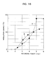
- Fig. 16 shows a result of the measurement of modulation degree which was obtained from data recorded with a pulsewidth of 220 n sec. using various powers while an optical disk provided by this embodiment was rotated at 600 rpm.
- a curve A shown in Fig. 16 is obtained by an optical disk of this embodiment and a curve B shows a characteristic of an optical disk not provided with the thin layer.
- the formation of the thin film disclosed by this invention increases recording sensitivity because of the reasons as follows. While voids on the recording layer is mainly formed by partial melting and diffusion of the recording layer, vaporization and sublimation slightly occur at the same time of the melting. These vaporized matters are cut off from escape by the presence of the thin layer composed of the polyvinyl alcohol and increase a pressure in a closed space. The diffusion is accelerated by the increased pressure so that good voids are formed with a result of the increase in the recording sensitivity.
- thermogravimetric analysis a thermal behavior of the recording layer (melting, vaporization and sublimation) depends on a material. Different materials maybe used depending on recording conditions required. For example, when a recording is to be carried out with lower power, materials which start to melt at a temperature of 230°C or less is preferably used, as described below.
- the result was good such that deterioration factor of a light reflecting factor of 0% was obtained with a reading power of 0.5 mW and the number of reading out of 10 5 .
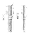
- Fig. 17 is a diagram explanatory of a fifth embodiment of the present invention.
- two single plates each composed of a substrate 11 with a recording layer 12 and a thin layer, and if necessary, an overcoat layer 14 formed thereon are integrally bonded together through an adhesive layer 23, e.g., an epoxy resin or a UV curing resin.
- Fig. 18 is a diagram explanatory of a sixth embodiment of the present invention, wherein, a single plate composed of a substrate 11 with a recording layer 12 and a thin layer 13, and, if necessary an overcoat layer 14 formed thereon is used solely
- Fig. 19 and Fig. 20 are enlarged cross sectional views of the vicinity of the recording layer.
- a void 22 is formed with the recording layer 12 partially and thinly remaining on the thin layer 13 side, whereas, in a recording pit shown in Fig. 20 the recording layer 12 even on the thin layer 13 side is almost perfectly heat-melted and forms a hollow-shaped void 24.
- the recording voids have different shapes depending on a material of the recording layer 12, a film thickness of the recording layer 12, a recording power or an irradiation time of a beam.
- voids are formed in the recording layer. While cases wherein voids are formed in the recording layer are described according to Fig.19 and Fig. 20, the voids are not always formed in the recording layer depending on the irradiation condition of a radiation beam, and the thin layer may be expanded toward the side opposite to the substrate is a thermal expansion.
- a spin coating was effected on a polycarbonate substrate to form a recording layer of 60 nm thick using a methyl alcohol solution (dye solution) containing 1.5 wt % of 1-butyl-2-(7-(1-butyl-2-indolinydene)-1,3,5-heptatriethyl)-3,3-dimethyl-indolinium-hexafluorophosphate.
- a 10% water solution containing a mixture of polyvinyl alcohol having a degree of saponification of 88.0% and a degree of polymerization of 1700 and bichromate ammonium of 10% with respect to the polyvinyl alcohol was prepared.
- This thin layer forming solution was applied on the recording layer by a spin coating to form a thin layer of 60 nm thick.
- ultraviolet rays were irradiated to the thin layer for 30 sec. from a position 15 cm apart therefrom with a power of 2.4 KW to form an air sandwich type optical disk using an organic dye by cross-linking and curing the polyvinyl alcohol.
- the conditions of an optical recording system using this optical disk were as follows. More specifically, a semiconductor laser having an oscillating wavelength of 830 nm and an objective lens having a NA of 0.53 were used. The above disk was rotated at 1800 rpm and data was recorded with a pulsewidth of 100 n/s and a recording power of 7 mW. As a result, a modulation degree of 81% was obtained.
- the optical data recording medium of the present invention is provided with the recording layer mainly composed of the organic dye formed on the transparent substrate and the thin layer formed on the recording layer serving as a pressurizing layer.
- the above recording layer is partially heated and reaches to a liquefied state to make the expansion of its volume.
- the state of the thin layer on the recording layer is not changed.
- the recording layer is pressurized and its interior temperature is further increased. This temperature increase causes the recording layer to be vaporized and its interior pressure to be further increased, and thus at last the thin layer as the pressurizing layer is deformed.
- the organic dye is separated from the surface of the substrate and no dye remains on the substrate and the laser is not substantially reflected.
- the heat energy generated in the recording layer by the irradiation of the laser beam is prevented from being discharged externally by the thin layer formed on the recording layer and accumulated internally. This accumulation of the energy at last pushes up the thin layer as the pressurizing layer and deforms it, and this deformation continues until the internal energy becomes lowered.
- the heat energy of the portion where the laser beam is irradiated is made uniform in the area and volume where the beam is irradiated and the overall irradiated portion reaches a high temperature. As a result, the dye material in the irradiated area is uniformly liquefied and/or vaporized and securely separated from the substrate.
- the material mainly composed of the organic dye separated from the substrate is distributed again to the thin layer as the pressurizing layer and/or absorbed and diffused in the thin layer.
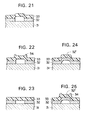
- Fig. 21 through Fig. 25 are schematic enlarged cross sectional views of a recording void.
- a portion of a recording layer 32 where a laser beam is irradiated disappears from the surface of a substrate 31 and the portion of a thin layer 33 corresponding to the disappeared portion is pushed upwardly in a substantially angular shape.
- a material of a recording layer 32 is partly attached again to the inner surface of a thin layer 33. While the recording layer 32' attached to the inner surface of the thin layer 33 is principally continuous to the recording layer 32, it is occasionally separated from the recording layer 32.
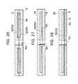
- Fig. 26 through Fig. 28 are cross sectional views of optical disks of eighth embodiment to tenth embodiment of the present invention.
- two single plates each composed of a substrate 31 with a recording layer 32, a thin layer 33 formed thereon are integrally bonded together through an elastic layer 38 of, e.g., polyurethane.
- the above recording single plate is bonded to a protective plate 39.
- 40 in Fig. 27 designates an air gap.
- an reflecting layer 41 is interposed between a substrate 31 and a recording layer 32, and a transparent protective plate 39 is used.
- 40 in Fig. 28 designates an air gap.
- the energy reflection ratio R is expressed by the following equation using the amplitude reflection factor r.
- R r 2 more specifically, assuming that an incident wave is represented by a 0 cos ⁇ and a composite wave is represented by a' cos ( ⁇ + ⁇ ), the energy reflection factor R is expressed by the following equation.
- R a′ a 0
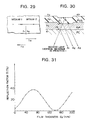
- Fig. 30 is a diagram explanatory of composite light composed of light reflected at respective interfaces of an optical data recording medium composed of a substrate with a recording medium composed of a substrate with a recording layer and a thin layer formed thereon sequentially. Respective symbols in Fig. 30 are designated as follows.
- a 1 r 12 cos ⁇
- a 2 t 12 r 23 t 21 cos ( ⁇ + 4 ⁇ n 2 d 2 ⁇ )
- a 3 t 12 t 23 r 30 t 32 t 21 cos ( ⁇ + 4 ⁇ (n 2 d 2 +n 3 d 1 ) ⁇ )
- composite light A 1 + A 2 + A 3 composed of light A 1 , A 2 , and A 3 reflected at the respective interfaces is obtained by the following equation.
- (A 1 +A 2 +A 3 ) r 12 cos ⁇ +t 12 r 23 t 21 cos ( ⁇ + 4 ⁇ n 2 d 2 ⁇ ) + t 12 t 23 r 30 t 32 t 21 cos ( ⁇ + 4 ⁇ (n 2 d 2 +n 3 d 1 ) ⁇ )
- This equation can be expressed by a' cos ( ⁇ + ⁇ ).
- Fig. 31 is a characteristic diagram illustrative of a change of the energy reflection factor R obtained when a film thickness d 1 of a PVA thin layer and a wavelength ⁇ of incident light are fixed and a film thickness d 2 of a recording layer is sequentially changed in the optical data recording medium shown in Fig. 30.
- Fig. 32 is a diagram explanatory of composite light composed of light reflected at respective interfaces of an optical data recording medium composed of a substrate having a recording layer and a thin layer sequentially formed thereon and a void defined at the intermediate portion of the recording layer. Respective symbols in Fig. 32 are designated as follows.
- a 1 r 12 cos ⁇
- a 2 t 12 r 20 t 21 cos ( ⁇ + 4 ⁇ n 2 d 4 ⁇ )
- a 4 t 12 t 20 t 02 r 23 t 20 t 02 t 21 cos( ⁇ + 4 ⁇ (n 2 d 4 +n 0 d 3 +n 2 d 2 ) ⁇
- a 5 t 12 t 20 t 02 t 23 r 30 t 32 t 20 t 02 t 21 cos ( ⁇ + 4 ⁇ (n 2 d 4 +n 0 d 3 +n 2 d 2 +n 3 d 1 ) ⁇ )
- composite light (A 1 + A 2 + A 3 + A 4 + A 5 ) composed of light A 1 - A 5 reflected at the respective interfaces is obtained by the following equation (15).
- (A 1 +A 2 +A 3 +A 4 +A 5 ) r 12 cos ⁇ + t 12 r 20 t 21 cos ( ⁇ + 4 ⁇ n 2 d 4 ⁇ ) + t 12 t 20 r 02 t 02 t 21 cos ( ⁇ + 4 ⁇ (n 2 d 4 +n 0 d 3 ) ⁇ ) + t 12 t 20 r 02 r 23 t 20 t 02 t 21 cos( ⁇ + 4 ⁇ (n 2 d 4 +n 0 d 3 +nd 2 ) ⁇ ) + t 12 t 20 t 02 t 23 r 30 t 32 t 20 t 02 t 21 cos ( ⁇ + 4 ⁇ (n 2 d 4 +n 0 d 3 +n 2 d 2 +n 3 d 1 ) ⁇ )
- Fig. 33 is a characteristic diagram illustrative of a change of the energy reflection factor R obtained when a film thickness d 1 of a PVA thin layer, film thicknesses d 2 and d 4 in a recording layer and a wavelength ⁇ of incident light are fixed and a void thickness d 3 is sequentially changed in the optical data recording medium shown in Fig. 33. Note that when the values of d 2 and d 4 are decreased in Fig. 33, the energy reflection factor R moves in close to a curve shown by symbols ⁇ , and when the values of d 2 and d 4 are increased, it moves in close to a curve shown by symbols ⁇ .
- a recording pit is read by a difference between a reflection factor of an unrecorded portion and a reflection factor of a recorded pit portion. Consequently, when a larger difference between the reflection factor of the unrecorded portion and the reflection factor of the recorded portion is provided, a larger modulation degree is obtained.
- An optical data recording medium having a recording element defined according to the void shape shown in Fig. 34 can be provided with a larger difference between the reflection factor of the unrecorded portion and that of the recorded pit portion larger than a difference between those of an optical data recording medium having a recording element defined according to a pit shape shown in Fig. 30. That is, a higher modulation degree can be obtained.
- Fig. 32 is an enlarged cross sectional view of another schematic example of a recording element of an embodiment of the present invention. As shown in Fig. 32, the thin layer of PVA is not deformed.
- Micro capsules can be used as described later to define voids in the intermediate portion in a recording layer in the thickness direction without deforming the thin layer.
- a thin layer which is finally returned to the original shape while it is temporary deformed in a recording process is referred to in an example of this embodiment.
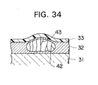
- Fig. 34 is an enlarged cross sectional view of another schematic example of a recording element of an embodiment of the present invention.
- a fibriform 43 may be formed depending on the material and physical properties of the recording layer 32 and the irradiating conditions of a laser beam.
- the void 42 is not always composed of a sinqle bubble but may be composed of the collection of a plurality of or a multiplicity of bubbles as a whole.
- a means for securely forming voids having a predetermined thickness includes a method of using micro capsules. More specifically, fine micro capsules are spin-coated together with the material of a recording layer, and after an optical data recording medium is formed, the surface film covering the capsules is broken by being vaporized or expanded in the recording layer to form the voids by irradiation of light or heat.
- the interior of the micro capsule may be hollow or filled with, for example, an autoxidation compound.
- An example of the capsule is composed of polyvinyl nitrate filled in the interior thereof and copolymer of gelatin and anionic polymer forming a coating film as a surface thereof.
- an optical data recording medium having a thin layer capable of being formed on a recording layer even if composed of an organic dye type recording material by a spin coating method of high productivity and a manufacturing method thereof, the optical data recording medium being able to reduce a production costs of an optical disk having a DRAW function.
- the present invention provides a reliable optical data recording medium having excellent sensitivity wherein voids are clearly shaped to enable signal outputs to rise sharply.
Description
- The present invention relates to an optical data recording medium such as an optical disk and a manufacturing method for this medium, and more specifically, to an optical data recording medium suitably used in a WO (write once) type optical disk provided, for example, with a recording layer composed of an organic dye type heat mode recording material and a manufacturing method for this medium.
- At present, CDs (compact disks) for reproducing music are widely used. Since, however, such CDs are used for reproduction only and do not have a so-called DRAW (direct read after write) function, a user cannot make a recording on such CDs or edit them. There is thus a strong desire for a CD having this DRAW function. Further, in an optical disk having applications other than a CD, a less expensive optical disk including the DRAW function is desired.
- A metal material such as Te for ablation type medium or a metal material such as In for a so-called phase changing type medium effecting dislocation from crystal to non-crystal is considered to be useful as a void type optical recording material having the DRAW function. Since, however, a recording layer composed of these metal type recording materials is formed using a thin film formation technique such as a vapor-deposition method or a sputtering method, there remains a problem in mass-productivity and cost.
- Thus, a pit type (heat mode WO type) organic dye type recording material which can be formed to a film by a spin coating method is considered more viable with respect to productivity.
- An optical disk, in particular, an optical disk using organic dye as a recording material must be provided with a protective layer for protecting a recording layer, and this protective layer is preferably formed by a spin coating method in consideration of for example manufacturing costs and mass productivity. Then, in general, a CD is provided with a protective layer composed of, e.g., an acrylate resin formed by a spin coating method.
- When, however, a UV curing type acrylate resin which is widely used and advantageous in material costs, productivity and characteristics is coated on a recording layer composed of the above organic dye type recording material, there are possibilities that the recording layer is damaged and, at worst, when a UV curing type resin is coated, the dye is melted and completely removed.
- In addition, there is a proposal to provide this kind of optical data recording medium which comprises a transparent substrate composed of a polymethyl methacrylate resin or glass having a thin film of a dye such as squarylium, thiopyrylium formed thereon and pits formed on the thin film by irradiation of a laser beam. (D. J. Gravesteijn et al., SPIE 420, 327, 1983).
- In addition to the above, there are many proposals for the material such as a cyanine dye (Japanese Patent Kokai (Laid-Open) No. 58-125246, Japanese Patent Kokai No. 59-85791), a naphtoquinone dye (Japanese Patent Kokai No. 58-224793), an azulenium dye (Japanese Patent Kokai No. 59-129954), a naphthalocyanin dye (Japanese Patent Kokai No. 61-25886). Further, another proposal uses a single state oxygen quencher together with the cyanine dye to improve an optical stability (Japanese Patent Kokai No. 59-67092). All of these proposals intend to record data by defining pits on a recording layer composed of a single dye layer.
- Further, there is a proposal that a reflecting layer is formed on a plastic film in a flattened layer, a recording layer composed of a mixture of dye and polymer is formed on the reflecting layer and recording pits are defined by irradiation of a laser beam (James W, Wheeler et al., SPIE 420, 39, 1983), a proposal that a recording layer composed of a mixture of dye and styrene oligomer is formed (A. Kuroiwa et al., Jap. J. Appl. Phys. 22, 340, 1983), and on all of which data are recorded by formation of pits.
- When a recording layer is composed of a single dye of these various organic dyes, the dye remains on the bottom portions of pits defined by irradiation of a laser beam and the laser beam irradiated at the portion where the dye remains is reflected. Therefore, there is no difference between reflection factors at a flat portion and that at a pit portion, and thus a sufficient modulation factor cannot be obtained. Further, since the pits have a rim portion of the edges thereof shaped to a gentle and obscure configuration, this recording medium has a problem in that a signal output does not rise sharply.
- Further, as described above, the recording medium provided with the recording layer composed of the mixture of the dye and polymer or the mixture of the dye and styrene oligomer has lower light absorption and light reflection than those of the recording layers composed of the single dye, and then has a lower modulation factor. Further, not only this recording medium requires a larger power when a laser beam is irradiated thereon but also the configuration of the pits thereof is not clearly defined like the recording medium using the single dye so that the medium has a problem in recording reliability.
- With the above pit type optical data recording medium, when a recording layer is formed on a transparent substrate and a laser beam is irradiated thereon, the recording layer is heat-melted at the portion where the beam is irradiated and the thickness of the recording layer is made thinner or the substrate is exposed at this portion.
- In reproduction, a signal can be read out because a reflection factor of the portion is lowered. Since, however, the difference between the reflection factors at a non-recorded portion and that at a recorded portion is small, a sufficient modulation factor cannot be obtained and reproduction errors are caused.
- In addition, there is also a known method that a metal film is expanded by a vapor pressure produced by partially heating an organic film by the irradiation of a laser beam thereby to form bubbles for recording data.
- Since, however, this method reproduces a signal by making use of reflection effected on a surface of a metal film and this metal film is formed by a thin film formation technique such as a vapor-deposition method or a sputtering method, there remains a problem in mass-productivity and cost.
- Conventionally, there is used a recording system wherein pits are defined by heat-melting and expanding a recording layer by irradiation of a laser beam. When a conventional dye and this irradiation are applied to a recording layer, declining of the viscosity according to the duration causes a restriction for good recording. As a means for solving this problem, there is an example wherein a material which is effectively subjected to a thermal effect by using a thermally unstable dye is employed. This thermally unstable material can improve sensitivity in recording, whereas it is degraded by reading light in reproduction. In addition, even if a thermally unstable material is used, a pit is only shaped to have an enlarged inner surface like a conical earthenware pat and it is impossible to define good pits having a clear pot edges.
- Further, the dye is usually unstable under high light conditions, in particular under sunlight, and thus this recording medium has a drawback that the dye is observed to be degraded.
- A process for manufacturing an optical recording medium comprising a heat-deformable optical recording layer and a protective layer of a transparent thermal and mechanical barrier layer are layered on the support thereof is disclosed in the U.S. Patent 4,340,655.
- In this process, said protective layer is formed on the recording layer by applying a water solution of a water-soluble polymer to the recording layer to be dried.
- However, this process has the following problems.
- (1) A water solution of the water-soluble polymer, in the case of production of an optical data recording medium by application of said solution to a recording layer to form a protective layer composed of said water soluble polymer, has the problems in that the recording material in the recording layer is dispersed or dissolved in water in said solution, or in that the material having wettability can not be used since the water of said solution permeate into the recording layer.
- (2) Although the recording material difficult to dissolve in water is used, it is impossible to produce a medium composed of the recording layer and the protective layer, unless the recording material of the recording layer is wettable to the application solution.
- (3) It is further necessary that a material having surface activity is used as a water soluble polymer component in the case that the recording material is water repellent.
-
- According to a first aspect of the present invention, there is provided an optical data recording medium comprising a transparent substrate, a recording layer formed on the substrate and a thin layer, 10 nm to 400 µm thick, formed on the recording layer, characterized in that the recording layer has a refraction factor higher than that of the substrate, and that the recording layer on exposure to light or heat caused by irradiation with light is capable of forming voids within the recording layer, or between the recording layer and the substrate. Additionally voids may be formed between the thin layer and the substrate.
- The optical data recording medium according to the invention has a high modulation factor capable of being produced at low cost. Further the presence of the thin layer over the recording layer provides protection for the recording layer.
- The optical data recording medium according to the present invention is characterized by having voids for signals defined in the recording layer or between the recording layer and the substrate. The thin layer may be substantially deformed to the opposite side of the substrate by heating the recording layer by a radiation beam irradiated from the substrate side or the side opposite to the substrate.
- The recording layer of the optical data recording medium according to the invention may suitably be composed of an organic dye type recording material, preferably of a cyanine type dye.
- The recording layer of the optical data recording medium may suitably be composed of an organic dye type recording medium and fibre-shaped connections are defined in the voids.
- The thin layer of the optical data recording medium according to the invention is suitably composed of a hydrophilic polymer, preferably of a cross-linked polyvinyl alcohol.
- In a particularly preferred optical data recording medium according to the invention the recording layer is capable of recording data through melting, expansion, decomposition, or sublimation and contains a cyanine dye which starts to be melted at a temperature of 100°C or more and within a range of a laser beam power of 10 mW or less and an infrared ray absorbing agent of 20 wt % or less with respect to the cyanine dye, which exhibits absorption in a wavelength region longer than that of the maximum absorption peak of the cyanine dye; and the thin layer is composed of a hydrophilic resin subjected to a heat treatment or a radiation beam irradiation treatment. This embodiment provides an optical data recording medium having a high recording sensitivity and resistance to high light condition.
- Preferably one of the recording layer and the thin layer is formed from a sparingly water-dispersible component the other is formed from a water-dispersible component. This provides an optical data recording medium which is provided with a protective layer which may be capable of being formed on a recording layer composed of an organic dye type recording material by a spin coating method and can reduce costs of an optical disk having the above DRAW function.
- Preferably the optical data recording medium according to the invention also comprises an overcoat layer composed of an acrylate resin formed on the thin layer.
- The optical data recording medium according to the invention suitably has a total thickness of 1.1 to 1.5 mm.
- In one embodiment, in a method of manufacturing an optical data recording medium according to the present invention wherein a recording layer is formed on a transparent substrate and a thin layer is formed on the recording layer for covering the same, and then voids are defined in the recording layer while the thin layer is substantially deformed to the opposite side of the substrate by heating the recording layer by a radiation beam irradiated from the substrate side or the side opposite to the substrate, the said method is characterized in that the above recording layer is composed of a material which is "neither easily dissolved nor easily dispersed in water" (referred to as "a difficult-to-dissolve-in-water property", hereinafter) and the above thin layer is composed of hydrophilic polymer, and the thin layer is subjected to a water-proofing treatment by a polymerization reaction.
- According to a second aspect of the invention, there is provided a method of manufacturing an optical data recording medium according to the first aspect of invention which comprises a transparent substrate and a recording layer and a thin layer formed on the transparent substrate characterized by forming the recording layer from a material slightly soluble in the aqueous solution used for application of the thin layer under the application conditions used; and forming the thin layer from an aqueous solution of protective film material by direct application onto the recording layer followed by drying.
- The recording layer may be formed from a material dissolved in non-aqueous solvent by direct application onto the substrate, followed by drying.
- The direct application method employed may be spin coating.
- Preferably one of the recording layer component and the thin layer component is formed from a water-insoluble material and the other is formed from a water-soluble material, both being formed by spin coating, followed by drying.
- According to a further aspect of the invention there is provided use of an optical data recording medium according to the first aspect of invention in write once recording wherein the recording layer is exposed to light or to heat caused by irradiation with light such that voids are formed within the recording layer or between the recording layer and the substrate.
- According to another aspect of the invention there is provided a process for write once recording on an optical data recording medium according to the invention, which process comprises exposing the recording layer of the optical data recording medium to light or to heat caused by irradiation with light such that voids are formed within the recording layer or between the recording layer and the substrate.
- Suitably the material used as the component of the recording layer in this invention is an organic dye material which is difficult to disperse and dissolve in water, very difficult to react with water, and little wettable to water.
- A material used for the thin, protective layer is a polymer such as polyvinylalcohol; which is water soluble, shows surface activity to said organic dye of recording layer in a coated water solution in a protective layer, to be wettable to said organic dye or recording layer.
- The thin layer used according to the invention composed of the above hydrophilic polymer can be formed by a spin coating method of high productivity without affecting the recording layer when the recording layer is composed of the organic dye type recording material which has a difficult-to-dissolve-in-water property. It is enough to be insoluble in water for a few seconds while the spin coating is being effected to laminate the hydrophilic polymer to be difficult to be dissolved in water for the recording layer mentioned above. Hence it is acceptable that the recording layer has a slight water solubility. In addition, since this thin layer is hydrophilic and has low solubility to an organic solvent, a UV curing type resin such as an acrylate resin can be formed on the thin layer as an overcoat layer without affecting the thin layer even if by a spin coating method, and this overcoat layer can also be formed by a spin coating method.
- According to the present invention, voids for signals are defined within the recording layer or between the recording layer and the substrate so that the modulation factor is increased by using an optical interference effect described in detail later thereby to provide highly reliable optical data recording medium.
- Further, the method of manufacturing an optical data recording medium using an organic dye compound as a material for the recording layer and where the recording layer is formed by applying the compound to the transparent substrate by spin coating can be operated at a low cost with improved productivity.
- Decomposition, sublimation and heat-melting must be effected in a low temperature range to form clear voids by an irradiation of a laser beam to the recording layer. Thus, a dye which is thermally unstable at a temperature of 230°C or less is preferably used, while when a dye which is thermally unstable at a temperature of 230°C or higher is used, the recording layer of high sensitivity cannot be obtained. The lower limit of the thermal instability is 100°C, which corresponds to a maximum temperature in a compartment of an automobile parking under the blazing sun in summer, and thus this temperature must be the lower limit temperature. On the other hand, the upper limit of 230°C is a temperature preferable to satisfy the recording conditions such as a light power of 10 mW or less, a linear velocity of 6 m/sec. or more and a light pulsewidth of about 100 n sec., and the light power exceeding 10 mW is inconvenient because of the increase in power consumption and also from a view point of the durability of a laser beam and costs.
- Further, a lower linear velocity results in inconvenience in e.g. a transfer speed. The light pulsewidth is related to the linear velocity, and a broader pulsewidth encountered with a higher linear velocity results in a lowered recording capacity. Therefore, the light pulsewidth is preferably about 100 n sec., although it has a relation to the linear velocity.
- In order to form voids effectively in short time, a melting dye must not be expanded two-dimensionally but must be expanded three-dimensionally. For this purpose, a hydrophilic polymer is cross-linked on the recording layer or a thermally deformable layer subjected to a heat treatment is formed thereon so that it receives heat from the recording layer when a laser beam is irradiated and protrudes toward the opposite side with respect to the substrate thereby to expand the dye three-dimensionally. At this time, the pressure in the thermally deformable layer is increased simultaneously by the dissolution and sublimation of the dye and the formation of voids is accelerated by the increase in pressure. In addition, a material used as the thermally deformable layer must be water-proof and moisture resistant.
- Since a cyanine dye or the like used is generally insoluble to water, the hydrophilic polymer used as a material of the thermally deformable layer does not damage the recording layer in lamination. Since, however, the thermally deformable layer is hydrophilic, it absorbs water in the air to be deformed and swelled. Therefore, the water-proof and moisture resistance of the thermally deformable layer is improved by, for example, a cross-link treatment by an addition of a cross-link agent, a heat treatment, a radiation treatment.
- The improvement of durability of the recording layer under the reading light beam radiation will be described below.
- The deterioration of the recording layer by a reproducing light beam includes a deterioration caused by heat of a laser beam and a deterioration caused by light. The thermal deterioration is restricted by providing a thermally deformable layer and transferring heat therethrough to it to reduce an accumulation of heat. The deterioration caused by light can be restricted by adding to the cyanine dye an infrared absorption agent which exhibits absorption in a wavelength region longer than water-proof and moisture resistant.
- Since a cyanine dye used is generally insoluble to water, the hydrophilic polymer used as a material of the thermally deformable layer does not damage the recording layer in lamination. Since, however, the thermally deformable layer is hydrophilic, it absorbs water in the air to be deformed and swelled. Therefore, the water-proof and moisture resistance of the thermally deformable layer is for example improved by a cross-link treatment by an addition of a cross-link agent, a heat treatment, a radiation treatment.
- The improvement of durability of the recording layer under the reading light beam radiation will be described below.
- The deterioration of the recording layer by a reproducing light beam includes a deterioration caused by heat of a laser beam and a deterioration caused by light. The thermal deterioration is restricted by providing a thermally deformable layer and transferring heat therethrough to it to reduce an accumulation of heat. The deterioration caused by light can be restricted by adding to the cyanine dye an infrared absorption agent which exhibits absorption in a wavelength region longer than that in the maximum absorption peak of the cyanine dye, the cyanine dye being changed to a stable energy state. When, however, an infrared absorbing agent of 20 wt % or more is contained in the cyanine dye, the stability of the cyanine dye adversely affects recording sensitivity, and that in the maximum absorption peak of the cyanine dye, the cyanine dye being changed to a stable energy state. When, however, an infrared absorbing agent of 20 wt % or more is contained in the cyanine dye, the stability of the cyanine dye adversely affects recording sensitivity, and sensitivity is lowered.
-
- Fig. 1 is an enlarged cross sectional view of a main part of an optical disk of the first embodiment according to the present invention;
- Fig. 2 is an enlarged cross sectional view of a main part of an optical disk of the second embodiment according to the present invention;
- Fig. 3 is a vertical cross sectional view of an air sandwich type optical disk of the third embodiment according to the present invention;
- Fig. 4 is an enlarged cross sectional view of an main part of the optical disk.
- Fig. 5 is a diagram illustrative of typical examples of T ○ in the general formula of organic dyes used in the embodiments;
- Fig. 6 is a diagram illustrative of typical examples of A and A' used in the general formula, likewise;
- Fig. 7 through Fig. 12 are diagrams illustrative of examples of organic dyes used in the embodiments;
- Fig. 13 is a characteristic diagram illustrative of a result of a thermogravimetric analysis of organic dyes;
- Fig. 14 is a schematic cross sectional view of a coating device used in the manufacture of the illustrated embodiments;
- Fig. 15 is a characteristic diagram illustrative of the variations of optical properties caused by differences of coating techniques;
- Fig. 16 is a characteristic diagram illustrative of a modification degree in the recording layers of the present invention and in that of a prior art;
- Fig. 17 is a vertical cross sectional view of a bonding type optical disk of the fifth embodiment according to the present invention;
- Fig. 18 is a vertical cross sectional view of a single plate type optical disk of the sixth embodiment according to the present invention;
- Figs. 19 and 20 are enlarged cross sectional views of the vicinity of a recording void;
- Fig. 21 to Fig. 25 are schematic enlarged cross sectional views of a recording void in an optical disk of the seventh embodiment according to the present invention;
- Fig. 26 is a vertical cross sectional view of an optical disk of the eighth embodiment according to the present invention;
- Fig. 27 is a vertical cross sectional view of an optical disk of the ninth embodiment according to the present invention;
- Fig. 28 is a vertical cross sectional view of an optical disk of the tenth embodiment according to the present invention;
- Fig. 29 is a diagram explanatory of an energy reflection factor R;
- Fig. 30 is a diagram explanatory of composite light composed of light reflected at respective interfaces of an optical data recording medium composed of a substrate with a recording layer and a thin layer sequentially formed thereof;
- Fig. 31 is a characteristic diagram illustrative of a change of an energy reflection factor when a film thickness of a recording layer of the optical data recording medium shown in Fig. 30 is changed;
- Fig. 32 is a diagram explanatory of composite light composed of light reflected at respective interfaces of an optical data recording medium composed of a substrate having a recording layer and a thin layer sequentially formed thereon and a void defined at the intermediate portion of the recording layer;
- Fig. 33 is a characteristic diagram illustrative of a change of an energy reflection factor R obtained when film thicknesses d2 and d4 are fixed and a void thickness d3 is sequentially changed in the optical data recording medium shown in Fig. 32;
- Fig. 34 is an enlarged cross sectional view of
another schematic example of a recording pit of the
twelfth embodiment according to the present invention;
- 1, 11, 31 ... a substrate
- 2, 12, 32 ... a recording layer
- 3, 13, 33 ... a thin layer
- 4, 37 ... an overcoat layer
- 18 ... a main body of a coating device
- 21 ... a housing
- 24, 42 ... a void
-
- The present invention will be described below in detail with reference to the embodiments illustrated in the drawings.
- Fig. 1 is a schematic partial and cross sectional view of an optical disk of the first embodiment, wherein 1 designates a transparent disk-shaped substrate, which may be of a transparent resin material such as polycarbonate, polymethyl methacrylate, polymethyl penten, epoxy resin or transparent ceramics such as glass, while in this embodiment a polycarbonate substrate is used. Note that la designates a center through hole of the substrate 1.
- Designated at 2 is a recording layer formed on the substrate 1 by a spin coating method and composed of an organic dye type heat mode recording material difficult-to-dissolve-in-water. This organic dye type heat mode recording material may be composed, for example, of a polymethyne dye, an anthraquinone dye, a cyanine dye, a phthalocyanine dye, a xanthene dye, a tri-phenyl methane dye, a pyrilium dye, an azulene dye, a metals containing azo dye. This embodiment uses a cyanine dye type material, and a methanol solution containing the cyanine dye is applied to the substrate 1 by a spin coating method to form the recording layer 2. The above difficulty-to-dissolve-in-water property of this recording layer 2 means that it is not dissolved in water for a few seconds while a spin coating of a thin layer composed of hydrophilic polymer described later is being effected and the recording layer 2 may be slightly dissolved in water.
- Designated at 3 is the thin layer composed of the hydrophilic polymer and formed on the recording layer 2 by a spin coating method, and this thin layer 3 may be composed of the following water-soluble resins.
- 1. polyvinyl alcohol
- 2. polyethylene oxide
- 3. polyacrylic acid
- 4. polystyrene-sodium-sulfonic acid
- 5. polyvinyl pyrolydone
- 6. polymethacrylic acid
- 7. polypropylene glycol
- 8. methyl cellulose
- 9. polyvinyl nitrate
-
- This embodiment uses the polyvinyl alcohol (PVA) as the thin layer 3, and a water solution containing the PVA is applied by a spin coating method to form the thin layer 3 having a film thickness of 120 nm.
- Note that the thin layer 3 must have the film thickness of 10 nm to 400 µm, preferably 60 nm (0.06 µm) or more. When the thickness is less than 60 nm, pin holes may be created and thus water and foreign matter penetrates through these pin holes and is deposited on the recording layer 2 and causes errors. In addition, when an overcoat layer is additionally formed on the thin layer 3, the overcoat material penetrates through these pin holes and attacks the recording layer 2. Therefore, the thin layer 3 preferably has the thickness of 60 nm or more. On the other hand, the upper limit thickness of the thin layer is limited to 400 µm or less because the CD standard specifies the thickness of a substrate to 1.2 ± 0.1 mm and the total thickness of a disk to 1.2 +0.3 / -0.1 mm at present. The film thickness of the thin layer 3 can be adjusted by the selection of e.g. a rotational mode of the substrate 1, a dropping condition, concentration, the atmosphere around a turn table when the spin coating of the PVA is effected.
- Incidentally, since the thin layer 3 is composed of the water-soluble polymer such as the PVA, its moisture resistance is lowered. Hence, the thin layer 3 is subjected to e.g. a cross-linking treatment to provide it with water-proof (moisture resistance) and heat resistance. More specifically, a cross-linking agent or the like is added into a water solution of the water soluble polymer, and after the thin layer 3 is formed, cross-linking reaction is effected by irradiation of light or a cross-linking reaction is effected by heating. Alternatively, the thin layer 3 with no addition of the cross-linking agent is heated and crystallized (for example, since the PVA is used in this embodiment, the PVA is denaturated) or subjected to other treatments so that it is made insoluble to water, water-proof and heat resistant.
- Since, however, the above cross-linking reaction effected by light irradiation which does not require the consideration of an adverse thermal effect on the substrate 1 and the recording layer 2 and is also excellent in operating performance, this embodiment employs a technique wherein chrome is added as a cross-linking agent and the cross-linking reaction is effected in the thin layer 3 by the irradiation of light.
- Examples of a cross-linking means are shown as follows and any arbitrary means can be employed as necessary.
- 1. addition, for example, of copper, boron, aluminum, titanium, zirconium, tin, vanadium, chrome as inorganic cross-linking agent
- 2. acetal formation with aldehydes
- 3. aldehyde formation of hydroxyl group
- 4. addition of activated vinyl compound
- 5. etherification with epoxide compound
- 6. reaction of dicarboxylic acid with acid catalyst
- 7. addition of succinic acid and sulfuric acid
- 8. addition of triethylene glycol and methyl acrylate acid
- 9. blending of polyacrylic acid and methyl vinyl ether-maleic acid copolymer
-
- Designated at 4 is an overcoat layer formed on the thin layer 3 by a spin coating method, and in this embodiment, an acrylate resin as a UV curing type resin is used and its film thickness is selected to be 100 µm. Note that the overcoat 4 may be composed of a suitable material other than the acrylate resin.
- In this embodiment, after the thin layer 3 and the overcoat layer 4 are formed in sequence, both the layers are irradiated by ultraviolet rays, the thin layer 3 is cross-linked and the overcoat layer 4 is polymerized to be provided with water-proof and heat resistance.
- When data was recorded to an optical disk manufactured as described above with a linear velocity of 1.25 m/sec. and a recording power of 5 mW and the data was reproduced with a reproducing power of 0.5 mW, a good recording/reproducing property was obtained. No increase in noise due to the existence of the thin layer 3 as an intermediate layer disposed under the overcoat layer 4 was observed.
- Further, it was confirmed that the heat-melted material of the recording layer was easily shed by the thin layer 3 and good voids were defined when a heat mode recording was carried out (when voids' were defined in the recording layer 2) because the thin layer 3 is hydrophilic. Note that a recorded void (pit) array had a length of 0.9 - 3.3 µm and intervals of 0.9 - 3.3 µm.
- Using the same polycarbonate substrate as that shown in the first embodiment, a spin coating was effected on the substrate to form a recording layer of 80 nm thick using a methyl alcohol solution as cyanine dye containing 1.5 wt % of 1-methyl-2-[7-(1-methyl 2-indolinydene) 1,3,5-heptatrienyl] 3,3-dibutyl-indolium-hexafluorophosphate.
- Separately from this operation, a 10% water solution containing a mixture of polyvinyl alcohol having a degree of saponification of 88.0% and a degree of polymerization of 1700 and bichromate ammonium of 10% with respect to the polyvinyl alcohol was prepared. This solution was applied to the recording layer by a spin coating to form a thin layer of 60 nm thick. After this thin layer was dried, ultraviolet rays were irradiated thereto for 30 sec. from a position 15 cm apart therefrom with a power of 2.4 KW to form an air sandwich type optical disk using an organic dye by cross-linking the above polyvinyl alcohol.
- Likewise, as an example for comparison, a water solution containing 15% of sodium 2-acrylamide-2-methyl propane-sulfonate polymer described in Japanese Patent Kokoku No. 1-14879 was prepared and applied to a dye recording layer to a thickness of 60 nm to form an air sandwich type optical disk.
- Recording properties were measured using a semiconductor laser having an oscillating wavelength of 830 nm and an objective lens having an NA (numerical aperture) of 0.53. The above optical disk was rotated at 1800 rpm and data was recorded with a pulsewidth of 100 ns and a recording power of 7 mW. As a result, a modulation degree of 49% was obtained for the optical disk using the sodium-2-acrylamide-2-methylpropane-sulfonate polymer, whereas the modulation degree for the optical disk provided with the thin layer of polyvinyl alcohol formed on the recording layer of cyanine dye was 80%.
- When a recording layer composed of cyanine dye is used in the recording carried out with a wavelength of 780 - 830 nm using a light source of a semiconductor laser, cross-linked polyvinyl alcohol having a softening point of 200°C or more is most preferably used as a thin layer material. The cross-linked polyvinyl alcohol has a softening point of 200 - 230°C. When, however, a material having a softening point of 200°C or less, an optical recording with a good C/N (carrier/noise) cannot be obtained.
- More specifically, since the cyanine dye used as a recording material in the present invention has the melting point or the decomposing temperature of 200 - 230°C, when a recording layer reaches this temperature by an irradiation of a laser beam, the dye layer is liquefied and vaporized to cause a thin layer where the laser beam is irradiated to be swelled, whereby a high C/N is obtained, and when the thin layer is formed by a material having a softening point of 200°C or more, the most preferable recording can be carried out.
- When, however, the thin layer is formed by a material having a softening point of 200°C or less such as the sodium-2-acrylamide-2-methylpropane-sulfonate polymer as described in Japanese Patent Kokoku No. 1-14879, a portion where the laser beam is irradiated melts even the thin layer together with the dye layer and defines holes, resulting in that a preferable swelling is not formed and the high C/N cannot be obtained, which is greatly different from the result of the present invention.
- According to the present invention, a dye material for a recording layer is strictly designed and further a material for a thin layer formed thereon is examined in detail to ensure that a portion of the recording layer where a laser beam is irradiated forms a preferable swelling to provide a high C/N, in a recording carried out by a semiconductor laser beam. As a result, polyvinyl alcohol is determined as the most preferable material, and after a thin film is formed on the dye, the film is cross-linked and subjected to a water-proofing treatment to form the recording layer.
- Fig. 2 shows a second embodiment. This embodiment is arranged to omit the above overcoat layer 4. In this embodiment, a thin layer 3 has a thickness of tens to four hundred µm and has been made water-proof and heat resistant by a cross-linking reaction. In this embodiment, a good recording/reproducing property is expected likewise.
- The resepctive embodiments described above can be formed by spin coating the thin layer 3 on the recording layer 2 without possibility of attack of the recording layer 2 composed of the organic dye type heat mode recording material and formed by a spin coating method.
- Note that in the above embodiments, while the recording layer 2 is composed of the organic dye type recording material, the hydrophilic polymer to be used in the present invention is applicable as a thin layer to be formed on a recording layer having various recording modes.
- This hydrophilic polymer can be applicable to an optical data recording medium other than the optical disk so that the present invention is not limited by a recording area mode or a recording speed control system.
- Fig. 3 is a vertical cross sectional view of an air sandwich type optical disk of a third embodiment of the present invention, and Fig. 4 is an enlarged cross sectional view of a main part of this optical disk.
- In Figs. 3 and 4, 11 designates a disk-shaped substrate composed of a transparent material, which may be composed of a transparent resin material such as polycarbonate, polymethyl methacrylate, polymethyl penten, epoxy resin or transparent ceramics such as glass, and, in this embodiment, a polycarbonate substrate is used. Note that 11a designates a center through hole of the substrate 11.
- Designated at 12 is a recording layer formed on the substrate 11 by a spin coating method and composed of an organic dye type heat mode recording material difficult-to-dissolve-in-water. This organic dye type heat mode recording material may be composed, for example, of a polymethyne dye, an anthraquinone dye, a cyanine dye, phthalocyanine dye, a xanthene dye, a triphenyl methane dye, a pyrylium dye, an azulene dye, a metals containing azo dye. This embodiment uses a cyanine dye type material, and a methanol solution containing the cyanine dye is applied to the substrate 11 by a spin coating method to form the recording layer 12.
- An indol type cyanine dye of cyanine type organic dyes which particularly has the following general formula is preferably used.

- In the formula, T ○ is a carbon chain to form a methyne chain and composed of a linear chain or polycyclic compound of C3 - C17, and a hydrogen atom attached to a carbon atom may be substrated by a halogen atom,(R" is a linear chain of C1 - C6 or an aromatic ring)

- A may be equal to or different from A' and both of them represent an aromatic ring, respectively. A hydrogen atom attached to a carbon atom may be substrated by -I, -Br, -Cl, -CnH2n+1 (n = 1 - 22), -OCH3,-NO2, and
 (R"' is a linear chain of a hydrocarbon or an aromatic ring)
- B may be equal to or different from B' and both of them represent -O-, -S-, -Se-, -CH=CH-, or(R"" is an alkyl group of C1 - C4 such as CH3, C2H5, C3H7, C4H9)

- R may be equal to or different from R', both of them represent an alkyl group of C1 - C22 and may be substrated by a sulfonyl group or a carboxyl group.
- X⊖ represents an anion containing a phosphor element, for example, hexafluoro-phosphate ion6 ⊖ or an anion such as I⊖, ClO4 ⊖ , Cl⊖, or BF4 ⊖.
- m and n represent 0 or integer of 1 through 3, respectively and have a relationship of m + n ≦ 3.
- The recording layer 12 can be formed on the disk substrate 11 by any method including a solution spin coating method, a vapor-deposition method or a laminating method by Langmuir-Blodgett or a suitable combination of these methods.
- While Fig. 5 shows typical examples of T ○ in the general formula, material having any formula other than these examples representing T ○ may be used.
- In addition, while Fig. 6 shows typical examples of A and A' in the general formula, material having any formula other than these examples representing A and A' may be used.
- 1 wt % of each of various organic dyes shown in Fig. 7 through Fig. 12 was dissolved in 1,2-dichloroethane and this solution was applied to a disk substrate composed of polymethyl methacrylate by a spinner method to form a recording layer and an optical disk was fabricated by a usual method.
- Various experiments prove that when T ○ in the above general formula shown in Fig. 7 through Fig. 12 is -CH=CH-CH= orthe heat resistance and recording sensitivity of the recording layer can be improved.

- In addition, when A and A' in the above general formula isthe reflection factor of the recording layer can be improved.

- Further, when B and B' in the above general formula is(R"" is an alkyl group of C1 - C4), the solubility of the organic dye can be increased.

- Furthermore, when R and R' in the above general formula is C4H9 or C5H11, the reflection factor of the recording layer can be increased.
- In particular, the cyanine dye, wherein T ○ in the general formula isA and A' are
 B and B' are
 R and R' are C2H5, and X is PF6 or I, has an excellent heat resistance, recording sensitivity, reflection factor and solubility, and then can be advantageously used.
- Next, an indol type cyanine dye was synthesized which was composed of 1-ethyl-2-[7-(1-ethyl-3,3-dimethyl-2-indolinydene)-1,3,5-heptatriethyl]-3,3-dimethyl-indolium and iodine ion I⊖, perchloric acid ion ClO4 ⊖ and hexafluoro-phosphate ion PF6 ⊖ were arranged, respectively, as anions. These various kinds of the organic dyes were subjected to a thermogravimetric analysis. The result of the analysis is shown in Fig. 13, wherein a change of weight of the dyes using I⊖ is shown by a dotted line, a change of weight of the dyes using ClO4 ⊖ is shown by a dot-dash-line and a change of weight of the dyes using PF6 ⊖ is shown by a solid line, respectively.
- Note that a differential scanning colorimeter Model TAS-100 of Rigaku Denki Co., Ltd. was used an measuring instrument, and samples were heated in nitrogen gas of a flow rate of 100 ml/min. with a temperature increase rate of 20°C/min. and temperatures at which the weight of the samples began to decrease were measured.
- Next, the conditions under which the recording layer is formed by a spin coating method will be described.
- Fig. 14 shows a schematic cross sectional view of a coating device, wherein 15 designates a motor, 16 designates a coating nozzle, 17 designates a turntable on which a disk substrate 11 is placed, 18 designate a main body of the coating device, 20 designates a pressurizing pump, and 21 designates a housing. While the housing 21 has the coating nozzle 16 passing therethrough, the vicinity of the turntable 17 isolated from the outside air by the housing 21 and the interior of the housing 21 is kept in a substantially perfectly sealed condition.
- The concentration of the dye or the dye composition is in the range of 0.4 wt % - 20.0 wt %. When this concentration exceeds 20.0 wt %, the final thickness of a film is excessively thick, voids are not successfully defined when recording is effected. On the other hand, when the concentration is less than 0.4 wt %, a drawback such as pin holes is caused.
- A rotational speed of the substrate 11, i.e., the rotational speed of the substrate for centrifuging out the excessive dye or the dye composition or the solvent is adjusted from 350 to 6500 rpm. When the rotational speed is less than 350 rpm, a centrifugal force is insufficient, and thus a drying speed of the inner circumference of the recording layer 12 is different from that of the outer circumference thereof with a result of an irregular film thickness, whereas when the rotational speed exceeds 6500 rpm, the film thickness is excessively thin, and thus a desired film thickness cannot be obtained.
- Further, the vicinity of the turntable 17 must be sealed, or almost perfectly sealed while the turntable 17 cannot be perfectly sealed since the dye or the dye composition is actually dropped, the turntable 17 being rotated. With this arrangement, a gas flow caused by the rotation of the turntable 17 can be minimized. This gas flow is shown by dot lines in Fig. 14 A condition under which the gas flow is generated greatly depends on a length of a distance d between the substrate 11 and the highest position 22 in the sealed housing, and thus the length d was determined to be one and half times a diameter of the substrate 11 or less. In addition, the partial pressure of the solvent in gas phase can be increased by keeping the turntable 17 in the sealed condition or in the almost perfectly sealed condition thereby the wettability of the solution to the substrate 11 is improved. With this arrangement, the uniformity of the film is greatly improved.
- Fig. 15 shows the variations of optical properties (reflection factor and transparency) in radial directions of cases wherein the turntables are sealed and cases of prior art.
- As apparent from Fig. 15 while the prior art shows optical properties varying ±10% or more in relative values with respect to average values, this embodiment can make variations limited to ±5% or less in relative values with respect to the average values, which is advantageous in that for example a uniform recording/reading property can be obtained.
- A spin coating time, i.e., a rotation time of the substrate 1 after the dye or the dye composition is dropped is determined to be 1 sec. or more. When the spin coating time is less than 1 sec. the dye or the dye composition cannot be sufficiently dispersed on a signal pattern forming surface.
- In addition, the spin coating can be carried out with different rotational speeds set in several stages as necessary. This is because a rotational speed suitable for forming a uniform film and another rotational speed for drying the film which is almost formed are required, and thus a rotation method composed of a first stage with a low rotational speed and a second stage with a rotational speed higher than the first stage is employed.
- The film is dried at a temperature of 10 - 115°C after the spin coating is completed.
- The time for drying is in the range from about 15 sec. to 135 sec. to make the result of temperature (°C) x time (sec.) to be less than about 1300.
- When the result is less than about 150 the film can not be completely dried. To the contrary the result which is more than about 1300 causes inconveniences such as thermal deformation of the substrate.
- Note that the rotation mode of the substrate can be arbitrarily adjusted in a process for dropping the dye or the dye composition. For example, a mode wherein a solution of the dye composition is almost uniformly coated on the substrate at rest and then the rotation of the substrate is accelerated to the maximum rotational speed in a moment, a mode wherein the solution of the dye or the dye composition is dropped from a clamping area to the substrate being rotated at a suitable rotational speed to the outer circumference thereof and the like can be employed.
- Returning to Fig. 4 again, wherein 13 designates a thin layer composed of a hydrophilic polymer material formed on the above recording layer 2 by a spin coating method and, for example, the following water-soluble resins can be used as this material.
- 1. polyvinyl alcohol
- 2. polyethylene oxide
- 3. polyacrylic acid
- 4. polystyrene-sodium-sulfonic acid
- 5. polyvinyl pyrrolidone
- 6. polymethacrylic acid
- 7. polypropylene glycol
- 8. methyl cellulose
- 9. polyvinyl nitrate
-
- In addition, the following thermoplastic synthetic resins can be also used as the thin layer 3.
- 1. fluoro resin such as poly-tera-fluoro ethylene; polychlorotrifluoroethylene; vinylidene fluoride; tetrafluoroethylene-hexafluoropropylene-copolymer; vinylidene fluoride-hexafluoropropylene-copolymer; vinylidene fluoride-chlorotrifluoroethylene-copolymer; tetrafluoroethylene-perfluoroalkyl vinyl ether-copolymer; tetrafluoroethylene-ethylene copolymer.
- 2. imide resin such as polyimide; polyamide-imide; polyester-imide.
- 3. amide resin such as nylon-6; nylon-11; nylon-12; nylon-66; nylon-610; mixture of nylon 610; nylon 66.
- 4. ethylene resin such as polyethylene; cross-linked polyethylene; ethylene-acrylic acid ester copolymer; ionomer resin.
- 5. polypropylene
- 6. styrene resin such as polystyrene; styrene-acrylonitrile copolymer; styrene-acrylonitrile-butadiene copolymer.
- 7. polyvinyl chloride
- 8. polyvinylidene chloride
- 9. polyvinyl acetate
- 10. polyvinyl acetal
- 11. polycarbonate
- 12. polyacetal
- 13. saturated polyester resin such as polyethylene-tetraphthalate; polybutylene-terephthalate.
- 14. polyphenylene oxide
- 15. polysulfone
-
- Further, the following rubbers can be used as the thin layer 13.
- 1. diene rubber such as styrene-butadiene rubber, butadiene rubber; isoprene rubber; acrylonitrile-butadiene rubber; chloroprene rubber.
- 2. olefine rubber such as butyl rubber; ethylene-propyrene rubber; acrylic rubber; chlorosulfonic polyethylene rubber; fluoro rubber.
- 3. silicone rubber
- 4. urethane rubber
- 5. polysulfide rubber
-
- In this embodiment, polyvinyl alcohol (PVA) is used as the thin film 13 and a spin coating of the water solution of the PVA is effected to form the thin film 13 having a film thickness of 120 nm.
- Incidentally, since the thin film 13 is composed of hydrophilic polymer such as PVA, it has a deteriorated moisture resistance. Therefore, as described above, the thin layer 13 is subjected to a cross-linking treatment to be provided with a water-proof (moisture resistance) a heat resistance by being made insoluble to water.
- Next, a fourth embodiment will be described. First, a polycarbonate substrate with a diameter of 130 mm was made by an injection molding method. A dye solution made by dissolving a cyanine dye of 0.5 wt % having the following molecular structure into methanol was applied to the substrate by a spin coating method and a recording layer was formed.

- The condition to effect the spin coating was as follows. While the substrate was rotated at 490 rpm, the dye solution was dropped to the center thereof. After the substrate was rotated for 30 sec. it was further rotated for 30 sec. at 3000 rpm. This spin coating was carried out using the coating device shown in Fig. 14, the housing having a volume of 5000 cm3 was sealed, and the length of d was determined to be 12 cm. After the spin coating was finished, the substrate was dried for 30 sec. or more at a room temperature to form the recording layer composed of the cyanine dye on the substrate.
- Next, a coating solution for a thin layer was prepared in such a manner that polyvinyl alcohol of 2.5 wt % was dissolved in water as a material for this thin layer, and further bichromate ammonium was added to the water as a cross-linking agent. This coating solution was dropped to the overall recording area of the substrate at rest, and then the substrate was rotated for 20 sec. at 2000 rpm to remove an excessive solution, and further it was rotated for 1 min. at 6000 rpm to accelerate the drying of the substrate. The coating device shown in Fig. 14 was also used for this spin coating.
- Ultraviolet rays were irradiated to the thin layer formed as described above to polymerize the polyvinyl alcohol for a water-proofing (moisture resistant) treatment. Note that a thickness of the thin layer must be 60 nm or more to prevent the recording layer from being affected by the ultraviolet rays.
- Fig. 16 shows a result of the measurement of modulation degree which was obtained from data recorded with a pulsewidth of 220 n sec. using various powers while an optical disk provided by this embodiment was rotated at 600 rpm. The modulation degree used here is defined as the degree of sensitivity of the recording layer, and it is represented by the following equation assuming that a reflection factor before recording is A and that after recording is B.
- A curve A shown in Fig. 16 is obtained by an optical disk of this embodiment and a curve B shows a characteristic of an optical disk not provided with the thin layer.
- As apparent from Fig. 16 the formation of the thin film disclosed by this invention increases recording sensitivity because of the reasons as follows. While voids on the recording layer is mainly formed by partial melting and diffusion of the recording layer, vaporization and sublimation slightly occur at the same time of the melting. These vaporized matters are cut off from escape by the presence of the thin layer composed of the polyvinyl alcohol and increase a pressure in a closed space. The diffusion is accelerated by the increased pressure so that good voids are formed with a result of the increase in the recording sensitivity.
- As apparent from a result of the above thermogravimetric analysis (Fig.13), a thermal behavior of the recording layer (melting, vaporization and sublimation) depends on a material. Different materials maybe used depending on recording conditions required. For example, when a recording is to be carried out with lower power, materials which start to melt at a temperature of 230°C or less is preferably used, as described below.
- With respect to a reproducing light resistant characteristic, the result was good such that deterioration factor of a light reflecting factor of 0% was obtained with a reading power of 0.5 mW and the number of reading out of 105.
- Fig. 17 is a diagram explanatory of a fifth embodiment of the present invention. In this embodiment, two single plates each composed of a substrate 11 with a recording layer 12 and a thin layer, and if necessary, an overcoat layer 14 formed thereon are integrally bonded together through an adhesive layer 23, e.g., an epoxy resin or a UV curing resin.
- Fig. 18 is a diagram explanatory of a sixth embodiment of the present invention, wherein, a single plate composed of a substrate 11 with a recording layer 12 and a thin layer 13, and, if necessary an overcoat layer 14 formed thereon is used solely
- Fig. 19 and Fig. 20 are enlarged cross sectional views of the vicinity of the recording layer.
- In a recording layer shown in Fig. 19, a void 22 is formed with the recording layer 12 partially and thinly remaining on the thin layer 13 side, whereas, in a recording pit shown in Fig. 20 the recording layer 12 even on the thin layer 13 side is almost perfectly heat-melted and forms a hollow-shaped void 24. The recording voids have different shapes depending on a material of the recording layer 12, a film thickness of the recording layer 12, a recording power or an irradiation time of a beam.
- While cases wherein voids are formed in the recording layer are described according to Fig.19 and Fig. 20, the voids are not always formed in the recording layer depending on the irradiation condition of a radiation beam, and the thin layer may be expanded toward the side opposite to the substrate is a thermal expansion.
- Next, a seventh embodiment will be described.
- A spin coating was effected on a polycarbonate substrate to form a recording layer of 60 nm thick using a methyl alcohol solution (dye solution) containing 1.5 wt % of 1-butyl-2-(7-(1-butyl-2-indolinydene)-1,3,5-heptatriethyl)-3,3-dimethyl-indolinium-hexafluorophosphate.
- Separately from this operation, a 10% water solution (thin layer forming solution) containing a mixture of polyvinyl alcohol having a degree of saponification of 88.0% and a degree of polymerization of 1700 and bichromate ammonium of 10% with respect to the polyvinyl alcohol was prepared. This thin layer forming solution was applied on the recording layer by a spin coating to form a thin layer of 60 nm thick.
- After the thin layer was dried, ultraviolet rays were irradiated to the thin layer for 30 sec. from a position 15 cm apart therefrom with a power of 2.4 KW to form an air sandwich type optical disk using an organic dye by cross-linking and curing the polyvinyl alcohol.
- The conditions of an optical recording system using this optical disk were as follows. More specifically, a semiconductor laser having an oscillating wavelength of 830 nm and an objective lens having a NA of 0.53 were used. The above disk was rotated at 1800 rpm and data was recorded with a pulsewidth of 100 n/s and a recording power of 7 mW. As a result, a modulation degree of 81% was obtained.
- Next, the states under which recording voids were formed will be described. As described above, the optical data recording medium of the present invention is provided with the recording layer mainly composed of the organic dye formed on the transparent substrate and the thin layer formed on the recording layer serving as a pressurizing layer. When a laser beam is irradiated to this optical data recording medium, the above recording layer is partially heated and reaches to a liquefied state to make the expansion of its volume. However, the state of the thin layer on the recording layer is not changed. As a result, the recording layer is pressurized and its interior temperature is further increased. This temperature increase causes the recording layer to be vaporized and its interior pressure to be further increased, and thus at last the thin layer as the pressurizing layer is deformed. When it reaches this critical state, however, the organic dye is separated from the surface of the substrate and no dye remains on the substrate and the laser is not substantially reflected.
- As described above, the heat energy generated in the recording layer by the irradiation of the laser beam is prevented from being discharged externally by the thin layer formed on the recording layer and accumulated internally. This accumulation of the energy at last pushes up the thin layer as the pressurizing layer and deforms it, and this deformation continues until the internal energy becomes lowered. In addition, the heat energy of the portion where the laser beam is irradiated is made uniform in the area and volume where the beam is irradiated and the overall irradiated portion reaches a high temperature. As a result, the dye material in the irradiated area is uniformly liquefied and/or vaporized and securely separated from the substrate.
- The material mainly composed of the organic dye separated from the substrate is distributed again to the thin layer as the pressurizing layer and/or absorbed and diffused in the thin layer.
- Fig. 21 through Fig. 25 are schematic enlarged cross sectional views of a recording void.
- In the case of Fig. 21, a portion of a recording layer 32 where a laser beam is irradiated disappears from the surface of a substrate 31 and the portion of a thin layer 33 corresponding to the disappeared portion is pushed upwardly in a substantially angular shape.
- In the case of Fig. 22 while a portion of a thin layer 33 is pushed upwardly like the thin layer in Fig. 21, an annular projection 34 is defined around the portion pushed upwardly.
- In the case of Fig. 23, while a portion of a recording layer 32 where a laser beam is irradiated disappears from the surface of a substrate 31, a thin layer 33 is not deformed.
- In the cases of Figs. 24 and 25, a material of a recording layer 32 is partly attached again to the inner surface of a thin layer 33. While the recording layer 32' attached to the inner surface of the thin layer 33 is principally continuous to the recording layer 32, it is occasionally separated from the recording layer 32.
- Fig. 26 through Fig. 28 are cross sectional views of optical disks of eighth embodiment to tenth embodiment of the present invention.
- In the eighth embodiment shown in Fig. 26, two single plates each composed of a substrate 31 with a recording layer 32, a thin layer 33 formed thereon are integrally bonded together through an elastic layer 38 of, e.g., polyurethane.
- In the ninth the embodiment shown in Fig. 27, the above recording single plate is bonded to a protective plate 39. Note that 40 in Fig. 27 designates an air gap.
- In the tenth embodiment shown in Fig. 28, an reflecting layer 41 is interposed between a substrate 31 and a recording layer 32, and a transparent protective plate 39 is used. Note that 40 in Fig. 28 designates an air gap.
- Next, an optical interference effect of an optical data recording medium will be described with references to Figs. 29 and 30.
- Fig. 29 is a diagram explanatory of an energy reflection factor R. Assuming that an amplitude reflection factor is represented by r12 and an amplitude transmissivity is represented by t12 when light travels from a medium 1 to a medium 2, the amplitude reflection factor r12 and the amplitude transmissivity t12 in vertical incidence are expressed by the following equations using reflection factors n1, n2 of the mediums 1 and 2.
- In addition, the energy reflection ratio R is expressed by the following equation using the amplitude reflection factor r.
- Using the above, reflection factors in the following respective states were calculated.
- Fig. 30 is a diagram explanatory of composite light composed of light reflected at respective interfaces of an optical data recording medium composed of a substrate with a recording medium composed of a substrate with a recording layer and a thin layer formed thereon sequentially. Respective symbols in Fig. 30 are designated as follows.
- PC :
- substrate of polycarbonate
- dye :
- recording layer of organic dye
- PVA :
- thin layer of polyvinyl alcohol
- air :
- air (air gap)
- n0 :
- refraction factor of air (n0 = 1)
- n1 :
- refraction factor PC (n1 = 1.6)
- n2 :
- refraction factor of dye (n2 = 2.7)
- n3 :
- refraction factor of PVA (n3 = 1.5)
- d1 :
- film thickness of PVA
- d2 :
- film thickness of dye
- A1 :
- light reflected at interface between PC and dye
- A2 :
- light reflected at interface between dye and PVA
- A3 :
- light reflected at interface between PVA and air
- Light reflected at the respective interfaces A1, A2, and A3 is expressed by the following equations.
- Therefore, composite light A1 + A2 + A3 composed of light A1, A2, and A3 reflected at the respective interfaces is obtained by the following equation.
- This equation can be expressed by a' cos ( + Δ).
- The energy reflection factor R is determined by solving the right side of the equation (8) = a' cos ( + Δ), representing a' by r, t, n, d, λ, inserting respective values in them, and squaring the (resulted value of a') (because a0 = 1).
- Fig. 31 is a characteristic diagram illustrative of a change of the energy reflection factor R obtained when a film thickness d1 of a PVA thin layer and a wavelength λ of incident light are fixed and a film thickness d2 of a recording layer is sequentially changed in the optical data recording medium shown in Fig. 30.
- Fig. 32 is a diagram explanatory of composite light composed of light reflected at respective interfaces of an optical data recording medium composed of a substrate having a recording layer and a thin layer sequentially formed thereon and a void defined at the intermediate portion of the recording layer. Respective symbols in Fig. 32 are designated as follows.
- n0 :
- refraction factor of air and a void (n0 = 1)
- d2 :
- thickness of the recording layer remaining between a PVA layer and the void
- d3 :
- void thickness
- d4 :
- thickness of the recording layer remaining between the void and a PC substrate
- A2 :
- light reflected at an interface between the recording layer having the film thickness of d4 and the void
- A3 :
- light reflected at an interface between the void and the recording layer having the film thickness of d2
- A4 :
- light reflected at an interface between the recording layer having the film thickness of d3 and the PVA layer
- A5 :
- light reflected at an interface between the PVA layer and air
- Light reflected at the respective interfaces A1 - A5 are expressed by the following equations.
- Therefore, composite light (A1 + A2 + A3 + A4 + A5) composed of light A1 - A5 reflected at the respective interfaces is obtained by the following equation (15).
- Fig. 33 is a characteristic diagram illustrative of a change of the energy reflection factor R obtained when a film thickness d1 of a PVA thin layer, film thicknesses d2 and d4 in a recording layer and a wavelength λ of incident light are fixed and a void thickness d3 is sequentially changed in the optical data recording medium shown in Fig. 33. Note that when the values of d2 and d4 are decreased in Fig. 33, the energy reflection factor R moves in close to a curve shown by symbols , and when the values of d2 and d4 are increased, it moves in close to a curve shown by symbols ▴.
- A recording pit is read by a difference between a reflection factor of an unrecorded portion and a reflection factor of a recorded pit portion. Consequently, when a larger difference between the reflection factor of the unrecorded portion and the reflection factor of the recorded portion is provided, a larger modulation degree is obtained. An optical data recording medium having a recording element defined according to the void shape shown in Fig. 34 can be provided with a larger difference between the reflection factor of the unrecorded portion and that of the recorded pit portion larger than a difference between those of an optical data recording medium having a recording element defined according to a pit shape shown in Fig. 30. That is, a higher modulation degree can be obtained.
- Note that the ranges of a film thicknesses of respective portions in Fig. 32 are as follows.
- The film thicknesses of the respective portions in Fig. 32:
d1 (PVA) 1 mm - 10 µm d2 (dye) 1 mm - 5 µm d3 (void thickness) 1 mm - 5 µm d4 (dye) 1 mm - 5 µm - Fig. 32 is an enlarged cross sectional view of another schematic example of a recording element of an embodiment of the present invention. As shown in Fig. 32, the thin layer of PVA is not deformed.
- Micro capsules can be used as described later to define voids in the intermediate portion in a recording layer in the thickness direction without deforming the thin layer.
- A thin layer which is finally returned to the original shape while it is temporary deformed in a recording process, is referred to in an example of this embodiment.
- Fig. 34 is an enlarged cross sectional view of another schematic example of a recording element of an embodiment of the present invention. As shown in Fig. 34, a fibriform 43 may be formed depending on the material and physical properties of the recording layer 32 and the irradiating conditions of a laser beam.
- In addition, the void 42 is not always composed of a sinqle bubble but may be composed of the collection of a plurality of or a multiplicity of bubbles as a whole.
- A means for securely forming voids having a predetermined thickness includes a method of using micro capsules. More specifically, fine micro capsules are spin-coated together with the material of a recording layer, and after an optical data recording medium is formed, the surface film covering the capsules is broken by being vaporized or expanded in the recording layer to form the voids by irradiation of light or heat. The interior of the micro capsule may be hollow or filled with, for example, an autoxidation compound.
- An example of the capsule is composed of polyvinyl nitrate filled in the interior thereof and copolymer of gelatin and anionic polymer forming a coating film as a surface thereof.
- As described above, according to the present invention, there are provided an optical data recording medium having a thin layer capable of being formed on a recording layer even if composed of an organic dye type recording material by a spin coating method of high productivity and a manufacturing method thereof, the optical data recording medium being able to reduce a production costs of an optical disk having a DRAW function. In addition, the present invention provides a reliable optical data recording medium having excellent sensitivity wherein voids are clearly shaped to enable signal outputs to rise sharply.
Claims (17)
- An optical data recording medium comprising a transparent substrate, a recording layer formed on the substrate and a thin layer, 10 nm to 400 µm thick, formed on the recording layer, characterized in that the recording layer has a refraction factor higher than that of the substrate, and that the recording layer on exposure to light or heat caused by irradiation with light is capable of forming voids within the recording layer, or between the recording layer and the substrate.
- An optical data recording medium according to claim 1, wherein the recording layer is composed of an organic dye type recording material.
- An optical data recording medium according to claim 2, wherein the recording material is composed of cyanine type dye.
- An optical data recording medium according to claim 1, wherein the recording layer is composed of an organic dye type recording material and fibre-shaped connections are defined in the voids.
- An optical data recording medium according to any preceding claim, wherein said thin layer is composed of a hydrophilic polymer.
- An optical data recording medium according to any preceding claim, wherein the thin layer is composed of cross-linked polyvinyl alcohol.
- An optical data recording medium according to any preceding claim, wherein the recording layer is capable of recording data through melting, expansion, decomposition, or sublimation and contains a cyanine dye which starts to be melted at a temperature of 100°C or more and within a range of a laser beam power of 10 mW or less and an infrared ray absorbing agent of 20 wt % or less with respect to the cyanine dye, which exhibits absorption in a wavelength region longer than that of the maximum absorption peak of the cyanine dye; and the thin layer is composed of a hydrophilic resin subjected to a heat treatment or a radiation beam irradiation treatment.
- An optical data recording medium according to any preceding claim, wherein one of the recording layer and the thin layer is formed from a sparingly water-dispersible component the other is formed from a water-dispersible component.
- An optical data recording medium according to any preceding claim, wherein an overcoat layer composed of an acrylate resin is formed on the thin layer.
- An optical data recording medium according to any preceding claim, wherein voids are further formed between the thin layer and substrate.
- An optical data recording medium according to any preceding claim, wherein the total thickness of the medium is 1.1 to 1.5 mm.
- A method of manufacturing an optical data recording medium according to claim 1, which comprises a transparent substrate and a recording layer and a thin layer formed on the transparent substrate characterized by forming the recording layer from a material slightly soluble in the aqueous solution used for application of the thin layer under the application conditions used; and forming the thin layer from an aqueous solution of protective film material by direct application onto the recording layer followed by drying.
- A method according to claim 12, wherein the recording layer is formed from a material dissolved in non-aqueous solvent by direct application onto the substrate, followed by drying.
- A method according to claim 12 or 13, wherein the direct application is by spin coating.
- A method according to claim 12, wherein one of the recording layer component and the thin layer component is formed from a water-insoluble material and the other is formed from a water-soluble material, both being formed by spin coating, followed by drying.
- Use of an optical data recording medium as defined in any one of claims 1 to 11 in write once recording wherein the recording layer is exposed to light or to heat caused by irradiation with light such that voids are formed within the recording layer or between the recording layer and the substrate.
- A process for write once recording on an optical data recording medium as defined in any one of claims 1 to 11 which process comprises exposing the recording layer of the optical data recording medium to light or to heat caused by irradiation with light such that voids are formed within the recording layer or between the recording layer and the substrate.
Applications Claiming Priority (15)
| Application Number | Priority Date | Filing Date | Title |
|---|---|---|---|
| JP15006588 | 1988-06-20 | ||
| JP150065/88 | 1988-06-20 | ||
| JP15006588 | 1988-06-20 | ||
| JP273221/88 | 1988-10-31 | ||
| JP27322188 | 1988-10-31 | ||
| JP27322188 | 1988-10-31 | ||
| JP2882/89 | 1989-01-11 | ||
| JP288289 | 1989-01-11 | ||
| JP288289 | 1989-01-11 | ||
| JP45300/89 | 1989-02-28 | ||
| JP4530089 | 1989-02-28 | ||
| JP4530089 | 1989-02-28 | ||
| JP6926589 | 1989-03-23 | ||
| JP69265/89 | 1989-03-23 | ||
| JP6926589 | 1989-03-23 |
Publications (3)
| Publication Number | Publication Date |
|---|---|
| EP0348122A2 EP0348122A2 (en) | 1989-12-27 |
| EP0348122A3 EP0348122A3 (en) | 1990-03-07 |
| EP0348122B1 true EP0348122B1 (en) | 1999-12-08 |
Family
ID=27518294
Family Applications (1)
| Application Number | Title | Priority Date | Filing Date |
|---|---|---|---|
| EP19890306168 Expired - Lifetime EP0348122B1 (en) | 1988-06-20 | 1989-06-19 | Optical data recording medium and manufacturing method thereof |
Country Status (3)
| Country | Link |
|---|---|
| US (1) | US5021276A (en) |
| EP (1) | EP0348122B1 (en) |
| DE (1) | DE68929107T2 (en) |
Families Citing this family (10)
| Publication number | Priority date | Publication date | Assignee | Title |
|---|---|---|---|---|
| US5023167A (en) * | 1990-03-08 | 1991-06-11 | Hoechst Celanese Corp. | Optical information card |
| US5139837A (en) * | 1990-03-08 | 1992-08-18 | Hoechst Celanese Corp. | Optical information medium exhibiting sharp threshold for marking and excellent cnr |
| JPH04259593A (en) * | 1991-02-13 | 1992-09-16 | Pioneer Electron Corp | Optical recording medium |
| JPH05128588A (en) * | 1991-05-16 | 1993-05-25 | Canon Inc | Optical recording medium, optical recording/reproducing method, information writing device and information record reproducer |
| US5904969A (en) * | 1995-07-07 | 1999-05-18 | Hitachi Maxell, Ltd. | Optical data recording medium and manufacturing method thereof |
| US20070003979A1 (en) * | 1998-10-30 | 2007-01-04 | Worthington Mark O | Trackable optical discs with concurrently readable analyte material |
| JP2001047746A (en) * | 1999-08-13 | 2001-02-20 | Sony Corp | Optical recording medium |
| JP2002170279A (en) * | 2000-11-30 | 2002-06-14 | Sony Corp | Optical recording medium, its manufacturing method and injection molding machine |
| JP2004039050A (en) * | 2002-07-01 | 2004-02-05 | Tdk Corp | Optical recording medium, and method and device for manufacturing the same |
| JP4170132B2 (en) | 2003-04-14 | 2008-10-22 | 松下電器産業株式会社 | Optical recording medium |
Citations (4)
| Publication number | Priority date | Publication date | Assignee | Title |
|---|---|---|---|---|
| US4190843A (en) * | 1976-03-19 | 1980-02-26 | Rca Corporation | Recording methods for a multilayer optical record |
| US4340655A (en) * | 1980-06-18 | 1982-07-20 | Eastman Kodak Company | Thermal and mechanical barrier layers for optical recording elements |
| US4577306A (en) * | 1980-02-25 | 1986-03-18 | Eastman Kodak Company | Method for optically writing and/or reading information on optical recording elements |
| EP0183570A2 (en) * | 1984-11-30 | 1986-06-04 | Nec Corporation | Optical recording medium and optical disc |
Family Cites Families (10)
| Publication number | Priority date | Publication date | Assignee | Title |
|---|---|---|---|---|
| US4101907A (en) * | 1977-08-29 | 1978-07-18 | Rca Corporation | Overcoat structure for optical video disc |
| JPS58125246A (en) | 1982-01-22 | 1983-07-26 | Ricoh Co Ltd | Laser recording medium |
| JPS59129954A (en) | 1983-01-17 | 1984-07-26 | Canon Inc | Optical recording medium |
| JPS58224793A (en) | 1982-06-25 | 1983-12-27 | Nec Corp | Optical recording medium |
| JPS5967092A (en) | 1982-10-11 | 1984-04-16 | Tdk Corp | Optical recording medium |
| JPH0613238B2 (en) | 1982-11-08 | 1994-02-23 | 株式会社リコー | Optical information recording medium |
| NL8300685A (en) * | 1983-02-24 | 1984-09-17 | Philips Nv | OPTICALLY READABLE INFORMATION CARRIER EQUIPPED WITH A CROSS-TURNED PLASTIC COATING. |
| US4639745A (en) * | 1984-01-11 | 1987-01-27 | Pioneer Electronic Corporation | Optical recording medium |
| JPS6125886A (en) | 1984-07-17 | 1986-02-04 | Yamamoto Kagaku Gosei Kk | Optical information recording medium |
| US4735839A (en) * | 1985-07-10 | 1988-04-05 | Ricoh Co., Ltd. | Optical information recording medium |
-
1989
- 1989-06-19 DE DE1989629107 patent/DE68929107T2/en not_active Expired - Fee Related
- 1989-06-19 US US07/367,721 patent/US5021276A/en not_active Expired - Lifetime
- 1989-06-19 EP EP19890306168 patent/EP0348122B1/en not_active Expired - Lifetime
Patent Citations (4)
| Publication number | Priority date | Publication date | Assignee | Title |
|---|---|---|---|---|
| US4190843A (en) * | 1976-03-19 | 1980-02-26 | Rca Corporation | Recording methods for a multilayer optical record |
| US4577306A (en) * | 1980-02-25 | 1986-03-18 | Eastman Kodak Company | Method for optically writing and/or reading information on optical recording elements |
| US4340655A (en) * | 1980-06-18 | 1982-07-20 | Eastman Kodak Company | Thermal and mechanical barrier layers for optical recording elements |
| EP0183570A2 (en) * | 1984-11-30 | 1986-06-04 | Nec Corporation | Optical recording medium and optical disc |
Non-Patent Citations (1)
| Title |
|---|
| DATABASE WPI Week 8715, Derwent Publications Ltd., London, GB; Class A32, AN 87-106210 & JP-A-62 054 853 (MATSUSHITA ELEC IND CO LTD) 10 March 1987 * |
Also Published As
| Publication number | Publication date |
|---|---|
| DE68929107D1 (en) | 2000-01-13 |
| DE68929107T2 (en) | 2000-04-06 |
| EP0348122A3 (en) | 1990-03-07 |
| EP0348122A2 (en) | 1989-12-27 |
| US5021276A (en) | 1991-06-04 |
Similar Documents
| Publication | Publication Date | Title |
|---|---|---|
| EP0385341B1 (en) | Optical recording medium | |
| EP0348122B1 (en) | Optical data recording medium and manufacturing method thereof | |
| EP0356140B1 (en) | Optical data recording medium and manufacturing apparatus and method thereof | |
| US4871649A (en) | Optical recording medium and optical recording method using the same | |
| AU744048B2 (en) | Optical recording medium | |
| JP3008406B2 (en) | Optical information recording medium and method of manufacturing the same | |
| JP2001184649A (en) | Optical recording system and optical recording medium | |
| JPH0332882A (en) | Device to manufacture optical information recording medium and its manufacture | |
| JP2530517B2 (en) | WDM optical recording medium, manufacturing method thereof, optical multiple recording method, and optical multiple recording / reproducing method | |
| JP2823209B2 (en) | Optical information recording medium and method of manufacturing the same | |
| JP2671141B2 (en) | Information recording medium and method of manufacturing the same | |
| JPH0827992B2 (en) | Optical information recording medium and optical information recording method using the same | |
| JPH0319147A (en) | Optical recording medium and optical recording method | |
| JP3059461B2 (en) | Information recording medium | |
| JP3087902B2 (en) | Information recording medium and method of manufacturing the same | |
| JPH03132391A (en) | Erasable high reflectivity optical recording medium | |
| JPS63281240A (en) | Information recording medium and its production | |
| JP2604273B2 (en) | Optical information recording method | |
| JPH0927146A (en) | Production of optical information recording medium and apparatus for production therefor | |
| JP2004087070A (en) | Write-once optical recording medium | |
| JP2000276787A (en) | Optical information recording medium and its production | |
| JPH03232132A (en) | Optical information recording medium | |
| JPH04252438A (en) | Optical information recording medium and production thereof | |
| JPH0492231A (en) | Optical information recording medium and production thereof | |
| JPH02223480A (en) | Optical information recording medium and production thereof |
Legal Events
| Date | Code | Title | Description |
|---|---|---|---|
| PUAI | Public reference made under article 153(3) epc to a published international application that has entered the european phase |
Free format text: ORIGINAL CODE: 0009012 |
|
| AK | Designated contracting states |
Kind code of ref document: A2 Designated state(s): DE FR GB |
|
| PUAL | Search report despatched |
Free format text: ORIGINAL CODE: 0009013 |
|
| AK | Designated contracting states |
Kind code of ref document: A3 Designated state(s): DE FR GB |
|
| RIN1 | Information on inventor provided before grant (corrected) |
Inventor name: TUBURAYA, TOSHIKANE Inventor name: FUJIWARA, HIDEO Inventor name: WATANABE, HITOSHI Inventor name: IUCHI, SHIN-ICHIRO Inventor name: SAITO, OSAMU Inventor name: SUENAGA, MASAHI Inventor name: KAMEZAKI, HISAMITSU |
|
| 17P | Request for examination filed |
Effective date: 19900807 |
|
| 17Q | First examination report despatched |
Effective date: 19930816 |
|
| GRAG | Despatch of communication of intention to grant |
Free format text: ORIGINAL CODE: EPIDOS AGRA |
|
| GRAG | Despatch of communication of intention to grant |
Free format text: ORIGINAL CODE: EPIDOS AGRA |
|
| GRAH | Despatch of communication of intention to grant a patent |
Free format text: ORIGINAL CODE: EPIDOS IGRA |
|
| GRAH | Despatch of communication of intention to grant a patent |
Free format text: ORIGINAL CODE: EPIDOS IGRA |
|
| GRAA | (expected) grant |
Free format text: ORIGINAL CODE: 0009210 |
|
| AK | Designated contracting states |
Kind code of ref document: B1 Designated state(s): DE FR GB |
|
| ET | Fr: translation filed | ||
| REF | Corresponds to: |
Ref document number: 68929107 Country of ref document: DE Date of ref document: 20000113 |
|
| PLBE | No opposition filed within time limit |
Free format text: ORIGINAL CODE: 0009261 |
|
| STAA | Information on the status of an ep patent application or granted ep patent |
Free format text: STATUS: NO OPPOSITION FILED WITHIN TIME LIMIT |
|
| 26N | No opposition filed | ||
| REG | Reference to a national code |
Ref country code: GB Ref legal event code: IF02 |
|
| PGFP | Annual fee paid to national office [announced via postgrant information from national office to epo] |
Ref country code: FR Payment date: 20060420 Year of fee payment: 18 |
|
| PGFP | Annual fee paid to national office [announced via postgrant information from national office to epo] |
Ref country code: GB Payment date: 20060614 Year of fee payment: 18 |
|
| PGFP | Annual fee paid to national office [announced via postgrant information from national office to epo] |
Ref country code: DE Payment date: 20060824 Year of fee payment: 18 |
|
| GBPC | Gb: european patent ceased through non-payment of renewal fee |
Effective date: 20070619 |
|
| REG | Reference to a national code |
Ref country code: FR Ref legal event code: ST Effective date: 20080229 |
|
| PG25 | Lapsed in a contracting state [announced via postgrant information from national office to epo] |
Ref country code: DE Free format text: LAPSE BECAUSE OF NON-PAYMENT OF DUE FEES Effective date: 20080101 |
|
| PG25 | Lapsed in a contracting state [announced via postgrant information from national office to epo] |
Ref country code: GB Free format text: LAPSE BECAUSE OF NON-PAYMENT OF DUE FEES Effective date: 20070619 |
|
| PG25 | Lapsed in a contracting state [announced via postgrant information from national office to epo] |
Ref country code: FR Free format text: LAPSE BECAUSE OF NON-PAYMENT OF DUE FEES Effective date: 20070702 |