EP0347906A2 - Self-diagnostic circuit for logic circuit block - Google Patents
Self-diagnostic circuit for logic circuit block Download PDFInfo
- Publication number
- EP0347906A2 EP0347906A2 EP89111371A EP89111371A EP0347906A2 EP 0347906 A2 EP0347906 A2 EP 0347906A2 EP 89111371 A EP89111371 A EP 89111371A EP 89111371 A EP89111371 A EP 89111371A EP 0347906 A2 EP0347906 A2 EP 0347906A2
- Authority
- EP
- European Patent Office
- Prior art keywords
- circuit
- diagnostic
- circuit blocks
- scan
- self
- Prior art date
- Legal status (The legal status is an assumption and is not a legal conclusion. Google has not performed a legal analysis and makes no representation as to the accuracy of the status listed.)
- Granted
Links
Images
Classifications
-
- H—ELECTRICITY
- H01—ELECTRIC ELEMENTS
- H01L—SEMICONDUCTOR DEVICES NOT COVERED BY CLASS H10
- H01L27/00—Devices consisting of a plurality of semiconductor or other solid-state components formed in or on a common substrate
- H01L27/02—Devices consisting of a plurality of semiconductor or other solid-state components formed in or on a common substrate including semiconductor components specially adapted for rectifying, oscillating, amplifying or switching and having at least one potential-jump barrier or surface barrier; including integrated passive circuit elements with at least one potential-jump barrier or surface barrier
- H01L27/04—Devices consisting of a plurality of semiconductor or other solid-state components formed in or on a common substrate including semiconductor components specially adapted for rectifying, oscillating, amplifying or switching and having at least one potential-jump barrier or surface barrier; including integrated passive circuit elements with at least one potential-jump barrier or surface barrier the substrate being a semiconductor body
-
- G—PHYSICS
- G01—MEASURING; TESTING
- G01R—MEASURING ELECTRIC VARIABLES; MEASURING MAGNETIC VARIABLES
- G01R31/00—Arrangements for testing electric properties; Arrangements for locating electric faults; Arrangements for electrical testing characterised by what is being tested not provided for elsewhere
- G01R31/28—Testing of electronic circuits, e.g. by signal tracer
- G01R31/317—Testing of digital circuits
- G01R31/3181—Functional testing
- G01R31/3185—Reconfiguring for testing, e.g. LSSD, partitioning
- G01R31/318533—Reconfiguring for testing, e.g. LSSD, partitioning using scanning techniques, e.g. LSSD, Boundary Scan, JTAG
- G01R31/318558—Addressing or selecting of subparts of the device under test
-
- G—PHYSICS
- G06—COMPUTING; CALCULATING OR COUNTING
- G06F—ELECTRIC DIGITAL DATA PROCESSING
- G06F11/00—Error detection; Error correction; Monitoring
- G06F11/22—Detection or location of defective computer hardware by testing during standby operation or during idle time, e.g. start-up testing
Definitions
- the present invention relates to a self-diagnostic circuit for diagnosing logic circuit blocks of a VLSI, and particularly to a self-diagnostic circuit that can select a particular one of logic circuit blocks to diagnose the quality of the block.
- VLSI very large scale integrated circuit
- a self-diagnostic system for diagnosing a logic circuit is based on signature analysis.
- An output register of a circuit block to be diagnosed forms a linear feedback shift register (LFSR).
- a test pattern generator generates test patterns, which are applied to the circuit block to be diagnosed. Outputs of the circuit block are sequentially applied to the LFSR. This operation is called “signature compression.” After the completion of a predetermined diagnostic sequence, the contents (signature of diagnosis) of the LFSR are compared with predetermined values to automatically diagnose the quality of the circuit block.
- a VLSI chip incorporating a self-diagnostic circuit may have a comparison circuit that compares a result of self-diagnosis with a predetermined value.
- a self-diagnostic result based on the comparison is represented with a simple quality signal that is outputted to an upper level controller or to the outside of the VLSI chip.
- the self-diagnostic result may be stored in a register that is readable from the outside of the chip. Then, the quality judgment is carried out under higher level control such as machine language instruction prorgam control, or with the use of an LSI tester.
- the register for storing the self-diagnostic result may be a register different from output registers of the circuit blocks that have been self-diagnosed, or the output registers of the circuit blocks that constitute an LFSR at the time of self-diagnosis may themselves be used as means for storing the diagnostic result.
- the reason of this is because the contents (signature) of the LFSR represent histories of patterns applied in the self-diagnosis. Therefore, it is common to use the output registers of the circuit blocks to be diagnosed as the means for storing the diagnostic result.
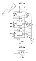
- Figure 1a is a block diagram showing a self-diagnostic circuit according to a prior art.
- the prior art self-diagnostic circuit comprises circuit blocks 1-1, 1-2 and 1-3 to be diagnosed, flip-flops (FFs) 2-1, 2-2 and 2-3 each of which indicates whether or not the diagnosis is being carried out, flip-flops (FFs) 3-1, 3-2 and 3-3 for storing diagnosis resultant data, OR gates 4-1, 4-2 and 4-3, and an AND gate 5.
- a reset signal R is inputted through an input line l1
- a start signal ST is inputted through an input line l2.
- End signals EN1, EN2 and EN3 are outputted through output lines l3, l4 and l5.
- "GOOD” resultant signals are outputted through lines l6, l7 and l8.
- a self-diagnosis "GOOD” resultant signal G is outputted through a line l9.
- Each of the FFs 2-1 to 2-3 and 3-1 to 3-3 is a D-type FF as shown in Fig. 1b.
- the FF latches "GOOD” resultant signals (G1, G2, G3) provided through a terminal A. Further, according to the clock signal CLK, the FF outputs the latched start signal ST, end signals EN1, EN2, and "GOOD” resultant signals (G1, G2, G3) through a terminal B.
- the clock signal CLK is not shown in Fig. 1a.
- a terminal B of the FF 2-1 outputs the signal of 1 to self-diagnose the circuit block 1-1 according to a signature analyzing method, etc.
- the block 1-1 After the completion of the diagnosis of the circuit block 1-1, the block 1-1 outputs the end signal EN1 and "GOOD” resultant signal G1.
- the resultant signal G1 is latched by the FF 3-1, and the end signal EN1 resets the FF 2-1 and starts the self-diagnosis of the circuit block 1-2.
- circuit blocks 1-1 to 1-3 are sequentially diagnosed.
- the "GOOD" resultant signals G1, G2 and G3 are sequentially latched by the FFs 3-1 to 3-3. Unless the reset signal R is inputted, the statuses of the FFs 3-1 to 3-3 are kept as they are. The contents of the FFs 3-1 to 3-3 are given to the AND gate 5.
- the self-diagnosis end signal EN3 of the circuit block 1-3 will be an overall self-diagnosis end signal.
- This end signal EN 3 and an overall "GOOD" resultant signal G (G1 G2 G3) are sent to an upper level control block (not shown) in the VLSI to complete the self-diagnostic operation.
- an output register of a certain circuit block to be self-diagnosed may commonly be used as an input register of the next circuit block to be diagnosed.
- N pieces circuit blocks to be self-diagnosed it is not necessary to provide a diagnosis execution indicating flip-flop (FF) for each of the N circuit blocks. Instead, it is possible to decode outputs of about log2N pieces of FFs to indicate the execution of diagnosis. It is also possible to use only one FF to indicate the parallel execution of self-diagnoses of a plurality of circuit blocks.
- the circuit blocks are sequentially diagnosed. Namely, they are diagnosed in a go-or-no-go way. Accordingly, the conventional system is not appropriate for analyzing the quality of complicated logic circuits and not sufficient to carry out a complicated self-diagnosis.
- the conventional diagnostic system cannot directly select a specific one among circuit blocks but it shall sequentially diagnose all the circuit blocks including the specific one.
- the self-diagnostic sequence is unavoidably complicated and expanded. Therefore, if the diagnostic sequence is disturbed in a certain block, diagnoses of the following blocks may be hindered to cause a serious problem.
- an object of the present invention is to provide a self-diagnostic system that can select a specific one among circuit blocks to diagnose the specific circuit block to effectively diagnose a plurality of the circuit blocks.
- the present invention provides a self-diagnostic circuit for diagnosing logic circuit blocks.
- the self-diagnostic circuit comprises a plurality of circuit blocks to be diagnosed, a plurality of first storage portions provided for indicating the execution of diagnosis of the circuit blocks, and second storage portions for storing results of diagnoses of the circuit blocks.
- the first and second storage portions and circuit blocks have a sequential diagnostic operation mode in which the circuit blocks are sequentially diagnosed according to a diagnosis starting signal, and a selective diagnosis mode in which a specific one among the circuit blocks is selected and diagnosed.
- the selective diagnosis mode is realized after supplying the logical value of the diagnosis starting signal and scan-in data with which the specific circuit block is separately selected and diagnosed, using a scan operation mode.
- the first and second storage portions and circuit blocks are connected in a predetermined order in a scan chain circuit.
- the storage portions and circuit blocks in the scan chain circuit are scanned, and data for selectively starting the diagnosis of the specific circuit block or selectively putting the specific circuit block under an execution state are set in the first and second storage portions and circuit blocks to selectively diagnose the specific circuit block.
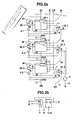
- Figure 2a is a block diagram showing a self-diagnostic circuit according to an embodiment realizing a self-diagnostic method of the invention.
- Figure 2b is a view showing the details of a flip-flop (FF) shown in Fig. 2a.
- FF flip-flop
- the self-diagnostic circuit comprises circuit blocks 1-1 to 1-3 to be diagnosed, flip-flops (FFs) 20-1 to 20-3 each indicating whether or not a diagnosis is under execution, flip-flops (FFs) 30-1 to 30-3 each storing diagnosis resultant data, OR gates 4-1 to 4-3, and an AND gate 9.
- the circuit blocks 1 1 to 1 3 incorporate circuits 40-1 to 40-3, respectively.
- Each of the circuits 40-1 to 40-3 comprises a diagnostic input pattern generating circuit and an end signal generating circuit that outputs an end signal (EN1, EN2 or EN3) for indicating the end of a diagnostic sequence.
- the embodiment has a selective diagnosis mode for selectively diagnosing a specific circuit block.
- a scan operation mode To realize the selective diagnosis mode, there is a scan operation mode.
- the FFs 20-1 to 20-3, FFs 30-1 to 30-3 and diagnostic input pattern generating and end signal generating circuits 40-1 to 40-3 are scanned according to a selection signal comprising a scan operation mode signal T to be described later to set the FFs and diagnostic input pattern generating and end signal generating circuits so that, after the scan operation mode is turned off, a specific one of the circuit blocks 1-1 to 1-3 will selectively be diagnosed.
- Each of the FFs 20-1 to 20-3 and 30-1 to 30-3 is constituted as shown in Fig. 2b.
- the FFs operate in the same manner as the D-type FFs shown in Fig. 1b.
- the FFs receive the scan-in data SI and output the scan in data SI from terminals B of the FFs at the rising edge of the clock signal CLK.
- a scan chain circuit To scan the FFs and circuit blocks with the scan-in data SI, a scan chain circuit connects the FFs and circuit blocks in the order of the diagnostic input pattern generating and end signal generating circuit 40-1, FF 20-1, FF 30-1, FF 30-2, the diagnostic input pattern generating and end signal generating circuit 40-3, FF 20-3 and FF 30-3.
- the embodiment employs two kinds of reset signals. Namely, a signal CR resets or initializes the FFs 20-1 to 20-3 and 30-1 to 30-3 and the diagnostic input pattern generating and end signal generating circuits 40-1 to 40-3 included in the scan chain, and a reset signal R initializes or resets the circuit blocks 1-1 to 1-3 to start the self-diagnosis.
- a signal CR resets or initializes the FFs 20-1 to 20-3 and 30-1 to 30-3 and the diagnostic input pattern generating and end signal generating circuits 40-1 to 40-3 included in the scan chain
- a reset signal R initializes or resets the circuit blocks 1-1 to 1-3 to start the self-diagnosis.
- the circuit of the embodiment shown in Fig. 2a additionally includes a line l10 for inputting the scan-in data SI, a line l11 for outputting a scan-out data SO, and a line l12 for inputting the reset signal CR.
- Fig. 2a the terminals shown in Fig. 2b for inputting the scan operation mode signal T and clock signal CLK are not shown for the sake of simplicity.
- the present invention is capable of diagnosing a particular one of the circuit blocks, for instance, the circuit block 1-3. This will be explained.
- the scan operation mode signal T supplied to each of the FFs 20-1 to 20-3 and 30-1 to 30-3 and diagnostic input pattern generating and end signal generating circuits 40-1 to 40-3 is set to 1 to establish the scan operation mode.
- the reset signal R is set to 1 and signal CR to 0 to required scan-in data SI be supplied from the outside for every clock cycle through the line l10.
- the scan-in data SI sequentially scan the diagnostic input pattern generating and end signal generating circuits 40-1 to 40-3 and FFs 20-1 to 20-3 and 30-1 to 30-3 in the order of the scan chain mentioned before.
- the scan operation mode signal T may be set to 0 so that those values are held in the FFs 20-1 to 20-3 and 30-1 to 30-3 and diagnostic input pattern generating and end signal generating circuits 40-1 to 40-3.
- the FF 20-3 will hold the value of 1.
- the self-diagnosis of the circuit block 1-3 corresponding to the FF 20-3 is carried out.
- a diagnosis "GOOD" resultant signal G3 from the circuit block 1-3 is fetched by the FF 30-3. Since the FFs 30-1 and 30-2 have held each 1, the signal G3 from an output of the FF 30-3 will cause the AND gate 9 to output an overall diagnosis "GOOD" resultant signal G.
- the embodiment can freely set various input signals to diagnose each circuit block independently of the other circuit blocks.
- a result of each diagnosis is easily understood by carrying out a predetermined number of diagnostic clock cycles having been set under the scan operation mode and by checking the signal G that indicates a result of the diagnosis.2
- the FFs 30-1 to 30-3 have been employed to store results of diagnoses.
- a register may be employed to store more detailed results of diagnoses.
- a value of an output register or of a part of it, of the diagnosed circuit block may be transferred to the register that substitutes for the FFs, to store a result of the diagnosis therein.
- the lines l6, l7 and l8 may be diagnostic result transfer lines (single or plural), and the FFs 30-1 to 30-3 may be diagnostic result storing registers.
- diagnostic result storing means is a register
- the AND gate 9 is not needed.
- This register for storing the diagnostic result may be a normal register or may be an LFSR having serial or parallel inputs. If the LFSR is used, results of all diagnoses can be handled with the single register.
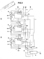
- Figure 3 is a view showing another embodiment of the invention, in which the diagnostic result storing means is a linear feedback shift register (LFSR) 51 with serial inputs.
- LFSR linear feedback shift register
- results of diagnoses of respective circuit blocks are transferred to the LFSR 51 that is a storage for storing a final overall diagnostic result.
- a result of diagnosis of each circuit block is expressed with the contents (plural bits) of an output register of the circuit block in question.
- the transfer operation to the LFSR 51 is achieved in plural clock cycles. Due to this, a diagnostic result transfer signal generating circuit is needed in addition to an end signal generating circuit.
- these two kinds of circuits and a diagnostic input pattern generating circuit are contained in each of circuits represented with numerals 41-1 to 41-3. Diagnostic result transfer signals of the circuit blocks are represented with reference marks TR1 to TR3, respectively.
- Reference marks l6 to l8 are transfer lines of the diagnostic results of the circuit blocks.
- transfer signals shall become 1 during a time period necessary for the transfer to activate writing operation with respect to the LFSR 51. Generally, this requires very small circuit addition. For example, if a diagnostic input pattern is provided by a count-up counter, a combination signal of proper bits of the counter or an overflow signal of the counter is generally used as an end signal, and also a transfer signal may be generated in the same manner.
- a selector 61 of Fig. 3 selects data to be taken in the LFSR from the transfer lines.
- a selection signal for the selector 61 is an output of a flip-flop (FF) that indicates an execution state of each diagnosis. (It is possible to omit some of the ouputs of the FFs). Therefore, in this embodiment, signals EN1 to EN3 that indicate the completion of respective diagnoses are activated after the completion of transfer of results of the diagnoses.
- the signal T is not shown in Fig. 3.
- the self-diagnostic according to the invention is applicable for logic circuit blocks that are controllable with microinstructions.
- the self-diagnosis under the control of microinstructions is somewhat special because a plurality of circuit blocks are diagnosed with a group of diagnostic microinstruction sequences.
- This technique basically requires only one flip-flop (FF) to indicate an overall execution state of the microinstruction diagnosis.
- Diagnosis of one circuit block may be distinguished from diagnoses of the other circuit blocks if the diagnostic microinstruction sequences are so formed to be clearly distinguished from each other. In this case, if initialization of each diagnostic sequence is done in first several steps of the sequence, it is more easy to distinguish the sequences from each other.
- an address input register of a ROM for storing the microinstructions is constituted to be scanned. Then, a first address of certain diagnostic microinstruction sequences for a certain circuit block may be set according to scanning operation.
- the certain circuit block can be diagnosed independently of the other circuit blocks.
- a temporal length of executing self-diagnosis of each microinstruction sequence is determined by the number of microloops. Namely, a microloop counter corresponds to a completion judging circuit of the diagnosis of each circuit block. If the microloop counter is made to be scanned, it is possible to control the completion judging circuit.
- the output register of the ROM for storing the microinstruction may be controlled by using the scan operation mode signal T to output NOP (NO OPERATION) signals for a necessary period of time.
- a particular one among circuit blocks can selectively be diagnosed independently of the other circuit blocks.
- an input register of a ROM for storing microinstructions is scanned to carry out the microinstruction self-diagnosis from an optional address.
- the self-diagnostic system of the present invention can be incorporated in a very large scale integrated circuit to effectively diagnose various logic blocks of the integrated circuit.
Abstract
Description
- The present invention relates to a self-diagnostic circuit for diagnosing logic circuit blocks of a VLSI, and particularly to a self-diagnostic circuit that can select a particular one of logic circuit blocks to diagnose the quality of the block.
- It is general to incorporate a diagnostic circuit in a VLSI (very large scale integrated circuit) to self-diagnose logic circuit blocks of the VLSI with a simple signal given externally to the diagnostic circuit. As VLSIs become more integrated, complicated and high functionl, a self-diagnostic system that can diagnose such a VLSI more easily is required.
- Generally, a self-diagnostic system for diagnosing a logic circuit is based on signature analysis. An output register of a circuit block to be diagnosed forms a linear feedback shift register (LFSR). A test pattern generator generates test patterns, which are applied to the circuit block to be diagnosed. Outputs of the circuit block are sequentially applied to the LFSR. This operation is called "signature compression." After the completion of a predetermined diagnostic sequence, the contents (signature of diagnosis) of the LFSR are compared with predetermined values to automatically diagnose the quality of the circuit block.
- There are various forms of judging a result of self-diagnosis. For example, as described in the above, a VLSI chip incorporating a self-diagnostic circuit may have a comparison circuit that compares a result of self-diagnosis with a predetermined value. A self-diagnostic result based on the comparison is represented with a simple quality signal that is outputted to an upper level controller or to the outside of the VLSI chip.
- Since it is not always necessary to implement the predetermined value on the chip, the self-diagnostic result may be stored in a register that is readable from the outside of the chip. Then, the quality judgment is carried out under higher level control such as machine language instruction prorgam control, or with the use of an LSI tester.
- The register for storing the self-diagnostic result may be a register different from output registers of the circuit blocks that have been self-diagnosed, or the output registers of the circuit blocks that constitute an LFSR at the time of self-diagnosis may themselves be used as means for storing the diagnostic result. The reason of this is because the contents (signature) of the LFSR represent histories of patterns applied in the self-diagnosis. Therefore, it is common to use the output registers of the circuit blocks to be diagnosed as the means for storing the diagnostic result.
- Figure 1a is a block diagram showing a self-diagnostic circuit according to a prior art. The prior art self-diagnostic circuit comprises circuit blocks 1-1, 1-2 and 1-3 to be diagnosed, flip-flops (FFs) 2-1, 2-2 and 2-3 each of which indicates whether or not the diagnosis is being carried out, flip-flops (FFs) 3-1, 3-2 and 3-3 for storing diagnosis resultant data, OR gates 4-1, 4-2 and 4-3, and an
AND gate 5. - In Fig. 1a, a reset signal R is inputted through an input line ℓ₁, and a start signal ST is inputted through an input line ℓ₂. End signals EN₁, EN₂ and EN₃ are outputted through output lines ℓ₃, ℓ₄ and ℓ₅. "GOOD" resultant signals are outputted through lines ℓ₆, ℓ₇ and ℓ₈. A self-diagnosis "GOOD" resultant signal G is outputted through a line ℓ₉.
- Each of the FFs 2-1 to 2-3 and 3-1 to 3-3 is a D-type FF as shown in Fig. 1b. According to a clock signal CLK, the FF latches "GOOD" resultant signals (G₁, G₂, G₃) provided through a terminal A. Further, according to the clock signal CLK, the FF outputs the latched start signal ST, end signals EN₁, EN₂, and "GOOD" resultant signals (G₁, G₂, G₃) through a terminal B. The clock signal CLK is not shown in Fig. 1a.
- To carry out the self-diagnosis in the arrangement of Fig. 1a, the reset signal R (=1) is given to the blocks 1-1 to 1-3 through the line ℓ₁ to initialize the circuit as a whole. Then, the FFs 2-1 to 2-3 and 3-1 to 3-3 are all reset. AT the same time, input registers, output registers, counters, etc., that are incorporated in the circuit blocks 1-1 to 1-3 but not shown in the figure are reset.
- After that, the reset signal R is returned to 0. The start signal ST (=1) is given through the line ℓ₂ so that the diagnosis may be started from the circuit block 1-1. A terminal B of the FF 2-1 outputs the signal of 1 to self-diagnose the circuit block 1-1 according to a signature analyzing method, etc.
- After the completion of the diagnosis of the circuit block 1-1, the block 1-1 outputs the end signal EN₁ and "GOOD" resultant signal G₁. Here, "G₁=1" represents "GOOD" while "G₁=0" represents "NO GOOD." The same will be applied to the signals G₂ and G₃. Then, the resultant signal G₁ is latched by the FF 3-1, and the end signal EN₁ resets the FF 2-1 and starts the self-diagnosis of the circuit block 1-2.
- In this way, the circuit blocks 1-1 to 1-3 are sequentially diagnosed. The "GOOD" resultant signals G₁, G₂ and G₃ are sequentially latched by the FFs 3-1 to 3-3. Unless the reset signal R is inputted, the statuses of the FFs 3-1 to 3-3 are kept as they are. The contents of the FFs 3-1 to 3-3 are given to the
AND gate 5. - The self-diagnosis end signal EN₃ of the circuit block 1-3 will be an overall self-diagnosis end signal. This
end signal EN 3 and an overall "GOOD" resultant signal G (G₁ G₂ G₃) are sent to an upper level control block (not shown) in the VLSI to complete the self-diagnostic operation. - The upper level control block judges that all the circuit blocks that have been self-diagnosed are normal if G=1 (i.e., G₁=1, G₂=1 and G₃=1), while the upper level control block judges that some of the circuit blocks are faulty if G=0.
- There are many forms of self-diagnosis other than the conventional example mentioned in the above. For example, an output register of a certain circuit block to be self-diagnosed may commonly be used as an input register of the next circuit block to be diagnosed. If there are many (N pieces) circuit blocks to be self-diagnosed, it is not necessary to provide a diagnosis execution indicating flip-flop (FF) for each of the N circuit blocks. Instead, it is possible to decode outputs of about log₂N pieces of FFs to indicate the execution of diagnosis. It is also possible to use only one FF to indicate the parallel execution of self-diagnoses of a plurality of circuit blocks. These superficial variations are not essential to the present invention, and the present invention is applicable to these variations.
- According to the conventional self-diagnostic system described in the above, the circuit blocks are sequentially diagnosed. Namely, they are diagnosed in a go-or-no-go way. Accordingly, the conventional system is not appropriate for analyzing the quality of complicated logic circuits and not sufficient to carry out a complicated self-diagnosis.
- In addition, the conventional diagnostic system cannot directly select a specific one among circuit blocks but it shall sequentially diagnose all the circuit blocks including the specific one.
- As VLSIs become further integrated, complicated and high functional, the self-diagnostic sequence is unavoidably complicated and expanded. Therefore, if the diagnostic sequence is disturbed in a certain block, diagnoses of the following blocks may be hindered to cause a serious problem.
- To solve the problem mentioned in the above, an object of the present invention is to provide a self-diagnostic system that can select a specific one among circuit blocks to diagnose the specific circuit block to effectively diagnose a plurality of the circuit blocks.
- In order to accomplish the object, the present invention provides a self-diagnostic circuit for diagnosing logic circuit blocks. The self-diagnostic circuit comprises a plurality of circuit blocks to be diagnosed, a plurality of first storage portions provided for indicating the execution of diagnosis of the circuit blocks, and second storage portions for storing results of diagnoses of the circuit blocks. The first and second storage portions and circuit blocks have a sequential diagnostic operation mode in which the circuit blocks are sequentially diagnosed according to a diagnosis starting signal, and a selective diagnosis mode in which a specific one among the circuit blocks is selected and diagnosed. The selective diagnosis mode is realized after supplying the logical value of the diagnosis starting signal and scan-in data with which the specific circuit block is separately selected and diagnosed, using a scan operation mode.
- The first and second storage portions and circuit blocks are connected in a predetermined order in a scan chain circuit. In the scan operation mode, the storage portions and circuit blocks in the scan chain circuit are scanned, and data for selectively starting the diagnosis of the specific circuit block or selectively putting the specific circuit block under an execution state are set in the first and second storage portions and circuit blocks to selectively diagnose the specific circuit block.
- These and other objects, features and advantages of the present invention will be more apparent from the following detailed description of preferred embodiments in conjunction with the accompanying drawings.
-
- Fig. 1a is a block diagram showing a self-diagnostic circuit according to a prior art;
- Fig. 1b is a schematic diagram a flip-flop (FF) shown in Fig. 1a;
- Fig. 2a is a block diagram showing a self-diagnostic circuit according to an embodiment of the invention;
- Fig. 2b is a schematic diagram showing a flip-flop (FF) shown in Fig. 2a; and
- Fig. 3 is a block diagram showing a modification of the self-diagnostic circuit of the invention.
- Figure 2a is a block diagram showing a self-diagnostic circuit according to an embodiment realizing a self-diagnostic method of the invention. Figure 2b is a view showing the details of a flip-flop (FF) shown in Fig. 2a.
- In Fig. 2a, the self-diagnostic circuit comprises circuit blocks 1-1 to 1-3 to be diagnosed, flip-flops (FFs) 20-1 to 20-3 each indicating whether or not a diagnosis is under execution, flip-flops (FFs) 30-1 to 30-3 each storing diagnosis resultant data, OR gates 4-1 to 4-3, and an AND
gate 9. The circuit blocks 1 1 to 1 3 incorporate circuits 40-1 to 40-3, respectively. Each of the circuits 40-1 to 40-3 comprises a diagnostic input pattern generating circuit and an end signal generating circuit that outputs an end signal (EN₁, EN₂ or EN₃) for indicating the end of a diagnostic sequence. - In addition to the sequential diagnostic operation mode explained with reference to Fig. 1a of the prior art, the embodiment has a selective diagnosis mode for selectively diagnosing a specific circuit block. To realize the selective diagnosis mode, there is a scan operation mode. The FFs 20-1 to 20-3, FFs 30-1 to 30-3 and diagnostic input pattern generating and end signal generating circuits 40-1 to 40-3 are scanned according to a selection signal comprising a scan operation mode signal T to be described later to set the FFs and diagnostic input pattern generating and end signal generating circuits so that, after the scan operation mode is turned off, a specific one of the circuit blocks 1-1 to 1-3 will selectively be diagnosed.
- Each of the FFs 20-1 to 20-3 and 30-1 to 30-3 is constituted as shown in Fig. 2b. When the scan operation mode signal T is 0, the FFs operate in the same manner as the D-type FFs shown in Fig. 1b. When the scan operation mode signal T is 1, the FFs receive the scan-in data SI and output the scan in data SI from terminals B of the FFs at the rising edge of the clock signal CLK.
- In connection with the FF shown in Fig. 2b, if the scan-in data SI is 1 with the scan operation mode signal T being 1 and if the clock signal CLK is changed from 0 to 1, the FF will take in the
value 1 of the scan-in data SI, and it hold the value (SI=1) if the scan operation mode signal T is changed to 0 before the clock signal CLK is next changed from 0 to 1. Then, a circuit block corresponding to the FF (20-1, 20-2 or 20-3) that is holding thevalue 1 will be diagnosed. - To scan the FFs and circuit blocks with the scan-in data SI, a scan chain circuit connects the FFs and circuit blocks in the order of the diagnostic input pattern generating and end signal generating circuit 40-1, FF 20-1, FF 30-1, FF 30-2, the diagnostic input pattern generating and end signal generating circuit 40-3, FF 20-3 and FF 30-3.
- Unlike the prior art shown in Fig. 1a, the embodiment employs two kinds of reset signals. Namely, a signal CR resets or initializes the FFs 20-1 to 20-3 and 30-1 to 30-3 and the diagnostic input pattern generating and end signal generating circuits 40-1 to 40-3 included in the scan chain, and a reset signal R initializes or resets the circuit blocks 1-1 to 1-3 to start the self-diagnosis.
- Like numerals represent like elements and like input/output lines in Figs. 1a and 2a. The circuit of the embodiment shown in Fig. 2a additionally includes a line ℓ₁₀ for inputting the scan-in data SI, a line ℓ₁₁ for outputting a scan-out data SO, and a line ℓ₁₂ for inputting the reset signal CR.
- In Fig. 2a, the terminals shown in Fig. 2b for inputting the scan operation mode signal T and clock signal CLK are not shown for the sake of simplicity.
- Operation of the embodiment will be explained.
- When the scan operation mode signal T is set to 0 and when the reset signals R and CR are simultaneously turned on, i.e., set to 1 to initialize the circuit as a whole. After that these signals are again turned off. Then, a starting signal ST may be set to 1 to start the self-diagnostic sequence. Under this situation, similar to the prior art shown in Fig. 1a, the circuit blocks 1-1 to 1-3 are sequentially diagnosed. Since the operation is the same as that of the prior art, it will not be repeatedly explained.
- In addition to the sequential diagnosis, the present invention is capable of diagnosing a particular one of the circuit blocks, for instance, the circuit block 1-3. This will be explained.
- The scan operation mode signal T supplied to each of the FFs 20-1 to 20-3 and 30-1 to 30-3 and diagnostic input pattern generating and end signal generating circuits 40-1 to 40-3 is set to 1 to establish the scan operation mode. The reset signal R is set to 1 and signal CR to 0 to required scan-in data SI be supplied from the outside for every clock cycle through the line l₁₀. The scan-in data SI sequentially scan the diagnostic input pattern generating and end signal generating circuits 40-1 to 40-3 and FFs 20-1 to 20-3 and 30-1 to 30-3 in the order of the scan chain mentioned before. When the FFs 20-1 to 20-3 are set to 0, 0 and 1, respectively, the FFs 30-1 to 30-3 to 1, 1 and 0, respectively, and the diagnostic input pattern generating and end signal generating circuits 40-1 to 40-3 to proper initial values, the scan operation mode signal T may be set to 0 so that those values are held in the FFs 20-1 to 20-3 and 30-1 to 30-3 and diagnostic input pattern generating and end signal generating circuits 40-1 to 40-3. Particularly, the FF 20-3 will hold the value of 1. Then, the self-diagnosis of the circuit block 1-3 corresponding to the FF 20-3 is carried out. A diagnosis "GOOD" resultant signal G₃ from the circuit block 1-3 is fetched by the FF 30-3. Since the FFs 30-1 and 30-2 have held each 1, the signal G₃ from an output of the FF 30-3 will cause the AND
gate 9 to output an overall diagnosis "GOOD" resultant signal G. - In this way, the embodiment can freely set various input signals to diagnose each circuit block independently of the other circuit blocks. A result of each diagnosis is easily understood by carrying out a predetermined number of diagnostic clock cycles having been set under the scan operation mode and by checking the signal G that indicates a result of the diagnosis.2
- In the embodiment, the FFs 30-1 to 30-3 have been employed to store results of diagnoses. Instead of the FFs 30-1 to 30-3, a register may be employed to store more detailed results of diagnoses. Just after the completion of self-diagnosis of each circuit block, a value of an output register or of a part of it, of the diagnosed circuit block may be transferred to the register that substitutes for the FFs, to store a result of the diagnosis therein. In this case, the lines l₆, l₇ and l₈ may be diagnostic result transfer lines (single or plural), and the FFs 30-1 to 30-3 may be diagnostic result storing registers.
- In the above case, it is preferable to read the contents ("GOOD" signals G₁ to G₃ each represented by an array of plural bits) of the respective registers separately. It is not meaningful to make a simple "GOOD" signal from G₁ to G₃, as was seen in the prior art.
- If the diagnostic result storing means is a register, the AND
gate 9 is not needed. This register for storing the diagnostic result may be a normal register or may be an LFSR having serial or parallel inputs. If the LFSR is used, results of all diagnoses can be handled with the single register. - Figure 3 is a view showing another embodiment of the invention, in which the diagnostic result storing means is a linear feedback shift register (LFSR) 51 with serial inputs. In this embodiment, results of diagnoses of respective circuit blocks are transferred to the
LFSR 51 that is a storage for storing a final overall diagnostic result. A result of diagnosis of each circuit block is expressed with the contents (plural bits) of an output register of the circuit block in question. The transfer operation to theLFSR 51 is achieved in plural clock cycles. Due to this, a diagnostic result transfer signal generating circuit is needed in addition to an end signal generating circuit. In Fig. 3, these two kinds of circuits and a diagnostic input pattern generating circuit are contained in each of circuits represented with numerals 41-1 to 41-3. Diagnostic result transfer signals of the circuit blocks are represented with reference marks TR₁ to TR₃, respectively. Reference marks l₆ to l₈ are transfer lines of the diagnostic results of the circuit blocks. - These transfer signals shall become 1 during a time period necessary for the transfer to activate writing operation with respect to the
LFSR 51. Generally, this requires very small circuit addition. For example, if a diagnostic input pattern is provided by a count-up counter, a combination signal of proper bits of the counter or an overflow signal of the counter is generally used as an end signal, and also a transfer signal may be generated in the same manner. - A
selector 61 of Fig. 3 selects data to be taken in the LFSR from the transfer lines. A selection signal for theselector 61 is an output of a flip-flop (FF) that indicates an execution state of each diagnosis. (It is possible to omit some of the ouputs of the FFs). Therefore, in this embodiment, signals EN₁ to EN₃ that indicate the completion of respective diagnoses are activated after the completion of transfer of results of the diagnoses. To enable read operation with a scan operation mode signal T=1, a feedback loop of theLFSR 51 is electrically cut off with the scan operation mode signal T (=1) so that theLFSR 51 may become a register that allows a normal scan operation. The signal T is not shown in Fig. 3. - The self-diagnostic according to the invention is applicable for logic circuit blocks that are controllable with microinstructions. The self-diagnosis under the control of microinstructions is somewhat special because a plurality of circuit blocks are diagnosed with a group of diagnostic microinstruction sequences. This technique basically requires only one flip-flop (FF) to indicate an overall execution state of the microinstruction diagnosis. Diagnosis of one circuit block may be distinguished from diagnoses of the other circuit blocks if the diagnostic microinstruction sequences are so formed to be clearly distinguished from each other. In this case, if initialization of each diagnostic sequence is done in first several steps of the sequence, it is more easy to distinguish the sequences from each other.
- With this sort of arrangement of the diagnostic microinstruction sequences, an address input register of a ROM for storing the microinstructions is constituted to be scanned. Then, a first address of certain diagnostic microinstruction sequences for a certain circuit block may be set according to scanning operation. By executing the certain microinstruction sequence, the certain circuit block can be diagnosed independently of the other circuit blocks. A temporal length of executing self-diagnosis of each microinstruction sequence is determined by the number of microloops. Namely, a microloop counter corresponds to a completion judging circuit of the diagnosis of each circuit block. If the microloop counter is made to be scanned, it is possible to control the completion judging circuit.
- To prevent abnormality from occurring during the scanning operation, the output register of the ROM for storing the microinstruction may be controlled by using the scan operation mode signal T to output NOP (NO OPERATION) signals for a necessary period of time.
- In summary, according to the present invention, a particular one among circuit blocks can selectively be diagnosed independently of the other circuit blocks. In a self-diagnosis system based on microinstruction control, an input register of a ROM for storing microinstructions is scanned to carry out the microinstruction self-diagnosis from an optional address.
- The self-diagnostic system of the present invention can be incorporated in a very large scale integrated circuit to effectively diagnose various logic blocks of the integrated circuit.
- Various modifications will become possible for those skilled in the art after receiving the teachings of the present disclosure without departing from the scope thereof.
Claims (4)
a scan chain circuit for connecting said first and second storage portions and circuit blocks in a predetermined order,
scanning operation under the scan operation mode being carried out through the scan chain circuit to set data in said first and second storage portions and in the diagnostic input pattern generating and end signal generating circuits of said circuit blocks such that only a specific one of said circuit blocks will be selectively executed and diagnosed, then the scan operation mode being released to execute the selective diagnosis of the specific circuit block.
(a) a plurality of connected logic circuit blocks to be diagnosed, each of said circuit blocks having a circuit for generating a diagnostic input pattern of the circuit block in question and an end signal generating circuit for generating an end signal of the circuit block in question and each being diagnosed according to the end signal sent from another of said circuit blocks arranged in front of the circuit block in question;
(b) a first storage portion provided for indicating execution of diagnosis of said circuit blocks;
(c) a second storage portion corresponding to said circuit blocks and storing diagnostic results of said circuit blocks, said first and second storage portions selecting input signals to be held therein according to a scan operation mode signal; and
(d) a scan chain circuit for connecting said first and second storage portions and diagnostic input pattern generating and end signal generating circuits in a predetermined order,
scan-in data being supplied through said scan chain circuit to said first and second storage portions and diagnostic input pattern generating and end signal generating circuits to set data to the said storage portions and diagnostic input pattern generating and end signal generatng circuits,
while the scan-in data being supplied through said scan chain circuit to the said storage portions and diagnostic input pattern generating and end signal generating circuits, the scan operation mode signal being supplied, then, after desired data having been set to the said storage portions and diagnostic input pattern generating and end signal generatng circuits, the scan operation mode signal being released, thus selectively diagnosing a specific one of said circuit blocks corresponding to the specific ones of said storage portions and diagnostic input pattern generating and end signal generating circuits.
Applications Claiming Priority (2)
| Application Number | Priority Date | Filing Date | Title |
|---|---|---|---|
| JP15401788 | 1988-06-22 | ||
| JP154017/88 | 1988-06-22 |
Publications (3)
| Publication Number | Publication Date |
|---|---|
| EP0347906A2 true EP0347906A2 (en) | 1989-12-27 |
| EP0347906A3 EP0347906A3 (en) | 1991-03-27 |
| EP0347906B1 EP0347906B1 (en) | 1996-04-17 |
Family
ID=15575088
Family Applications (1)
| Application Number | Title | Priority Date | Filing Date |
|---|---|---|---|
| EP89111371A Expired - Lifetime EP0347906B1 (en) | 1988-06-22 | 1989-06-22 | Self-diagnostic circuit for logic circuit block |
Country Status (4)
| Country | Link |
|---|---|
| EP (1) | EP0347906B1 (en) |
| JP (1) | JPH077345B2 (en) |
| KR (1) | KR920009635B1 (en) |
| DE (1) | DE68926265T2 (en) |
Cited By (1)
| Publication number | Priority date | Publication date | Assignee | Title |
|---|---|---|---|---|
| EP0568239A2 (en) * | 1992-04-30 | 1993-11-03 | AT&T Corp. | Built-in self-test network |
Families Citing this family (2)
| Publication number | Priority date | Publication date | Assignee | Title |
|---|---|---|---|---|
| JP2002100738A (en) | 2000-09-25 | 2002-04-05 | Toshiba Corp | Semiconductor ic and method of automatic inserting test facilitating circuit |
| JP5353542B2 (en) * | 2009-08-06 | 2013-11-27 | 富士通セミコンダクター株式会社 | Semiconductor device and test method of semiconductor device |
Citations (4)
| Publication number | Priority date | Publication date | Assignee | Title |
|---|---|---|---|---|
| GB1536147A (en) * | 1975-07-02 | 1978-12-20 | Int Computers Ltd | Data processing systems |
| GB2022319A (en) * | 1978-06-02 | 1979-12-12 | Int Standard Electric Corp | Very large scale integrated circuit |
| EP0181011A2 (en) * | 1984-11-08 | 1986-05-14 | Monolithic Memories, Inc. | A method and circuit detecting the logic state of internal nodes in sequential logic circuits |
| US4710931A (en) * | 1985-10-23 | 1987-12-01 | Texas Instruments Incorporated | Partitioned scan-testing system |
Family Cites Families (1)
| Publication number | Priority date | Publication date | Assignee | Title |
|---|---|---|---|---|
| JPS61138177A (en) * | 1984-12-11 | 1986-06-25 | Fujitsu Ltd | Method for testing selection of plural apparatus |
-
1989
- 1989-06-22 EP EP89111371A patent/EP0347906B1/en not_active Expired - Lifetime
- 1989-06-22 KR KR1019890008649A patent/KR920009635B1/en not_active IP Right Cessation
- 1989-06-22 DE DE68926265T patent/DE68926265T2/en not_active Expired - Fee Related
- 1989-06-22 JP JP1160206A patent/JPH077345B2/en not_active Expired - Fee Related
Patent Citations (4)
| Publication number | Priority date | Publication date | Assignee | Title |
|---|---|---|---|---|
| GB1536147A (en) * | 1975-07-02 | 1978-12-20 | Int Computers Ltd | Data processing systems |
| GB2022319A (en) * | 1978-06-02 | 1979-12-12 | Int Standard Electric Corp | Very large scale integrated circuit |
| EP0181011A2 (en) * | 1984-11-08 | 1986-05-14 | Monolithic Memories, Inc. | A method and circuit detecting the logic state of internal nodes in sequential logic circuits |
| US4710931A (en) * | 1985-10-23 | 1987-12-01 | Texas Instruments Incorporated | Partitioned scan-testing system |
Cited By (2)
| Publication number | Priority date | Publication date | Assignee | Title |
|---|---|---|---|---|
| EP0568239A2 (en) * | 1992-04-30 | 1993-11-03 | AT&T Corp. | Built-in self-test network |
| EP0568239A3 (en) * | 1992-04-30 | 1997-04-09 | American Telephone & Telegraph | Built-in self-test network |
Also Published As
| Publication number | Publication date |
|---|---|
| DE68926265T2 (en) | 1996-10-02 |
| KR910001968A (en) | 1991-01-31 |
| JPH0277849A (en) | 1990-03-16 |
| EP0347906B1 (en) | 1996-04-17 |
| KR920009635B1 (en) | 1992-10-22 |
| JPH077345B2 (en) | 1995-01-30 |
| DE68926265D1 (en) | 1996-05-23 |
| EP0347906A3 (en) | 1991-03-27 |
Similar Documents
| Publication | Publication Date | Title |
|---|---|---|
| US4597042A (en) | Device for loading and reading strings of latches in a data processing system | |
| JP2868213B2 (en) | Logic circuit with individually testable logic module | |
| JP2746804B2 (en) | Integrated circuit test method and integrated circuit test apparatus | |
| US5598421A (en) | Method and system for tracking the state of each one of multiple JTAG chains used in testing the logic of intergrated circuits | |
| US5708773A (en) | JTAG interface system for communicating with compliant and non-compliant JTAG devices | |
| US5841867A (en) | On-chip programming verification system for PLDs | |
| US5173904A (en) | Logic circuits systems, and methods having individually testable logic modules | |
| EP0880708B1 (en) | I/o toggle test method using jtag | |
| US6671839B1 (en) | Scan test method for providing real time identification of failing test patterns and test bist controller for use therewith | |
| US7644333B2 (en) | Restartable logic BIST controller | |
| US5491666A (en) | Apparatus for configuring a subset of an integrated circuit having boundary scan circuitry connected in series and a method thereof | |
| JP5373403B2 (en) | Method and apparatus for testing a data processing system | |
| US6745359B2 (en) | Method of masking corrupt bits during signature analysis and circuit for use therewith | |
| US5819025A (en) | Method of testing interconnections between integrated circuits in a circuit | |
| US6223312B1 (en) | Test-facilitating circuit for information processing devices | |
| JPH03168841A (en) | Method and apparatus for identically discriminating integrated circuit chip | |
| US5150366A (en) | Reduced delay circuits for shift register latch scan strings | |
| US5189675A (en) | Self-diagnostic circuit for logic circuit block | |
| US4912395A (en) | Testable LSI device incorporating latch/shift registers and method of testing the same | |
| US4996691A (en) | Integrated circuit testing method and apparatus and integrated circuit devices for use therewith | |
| US5077740A (en) | Logic circuit having normal input/output data paths disabled when test data is transferred during macrocell testing | |
| US5673274A (en) | Test method for semiconductor device | |
| EP0209982A2 (en) | Digital integrated circuits | |
| EP0347906B1 (en) | Self-diagnostic circuit for logic circuit block | |
| EP0454052B1 (en) | Data processing device with test circuit |
Legal Events
| Date | Code | Title | Description |
|---|---|---|---|
| PUAI | Public reference made under article 153(3) epc to a published international application that has entered the european phase |
Free format text: ORIGINAL CODE: 0009012 |
|
| 17P | Request for examination filed |
Effective date: 19890622 |
|
| AK | Designated contracting states |
Kind code of ref document: A2 Designated state(s): DE FR GB |
|
| PUAL | Search report despatched |
Free format text: ORIGINAL CODE: 0009013 |
|
| AK | Designated contracting states |
Kind code of ref document: A3 Designated state(s): DE FR GB |
|
| 17Q | First examination report despatched |
Effective date: 19930303 |
|
| GRAA | (expected) grant |
Free format text: ORIGINAL CODE: 0009210 |
|
| AK | Designated contracting states |
Kind code of ref document: B1 Designated state(s): DE FR GB |
|
| REF | Corresponds to: |
Ref document number: 68926265 Country of ref document: DE Date of ref document: 19960523 |
|
| ET | Fr: translation filed | ||
| GRAH | Despatch of communication of intention to grant a patent |
Free format text: ORIGINAL CODE: EPIDOS IGRA |
|
| PLBE | No opposition filed within time limit |
Free format text: ORIGINAL CODE: 0009261 |
|
| STAA | Information on the status of an ep patent application or granted ep patent |
Free format text: STATUS: NO OPPOSITION FILED WITHIN TIME LIMIT |
|
| 26N | No opposition filed | ||
| PGFP | Annual fee paid to national office [announced via postgrant information from national office to epo] |
Ref country code: FR Payment date: 19970610 Year of fee payment: 9 |
|
| PGFP | Annual fee paid to national office [announced via postgrant information from national office to epo] |
Ref country code: DE Payment date: 19970630 Year of fee payment: 9 |
|
| REG | Reference to a national code |
Ref country code: GB Ref legal event code: 746 Effective date: 19981010 |
|
| PG25 | Lapsed in a contracting state [announced via postgrant information from national office to epo] |
Ref country code: FR Free format text: LAPSE BECAUSE OF NON-PAYMENT OF DUE FEES Effective date: 19990226 |
|
| PG25 | Lapsed in a contracting state [announced via postgrant information from national office to epo] |
Ref country code: DE Free format text: LAPSE BECAUSE OF NON-PAYMENT OF DUE FEES Effective date: 19990401 |
|
| REG | Reference to a national code |
Ref country code: FR Ref legal event code: ST |
|
| REG | Reference to a national code |
Ref country code: GB Ref legal event code: IF02 |
|
| PGFP | Annual fee paid to national office [announced via postgrant information from national office to epo] |
Ref country code: GB Payment date: 20070620 Year of fee payment: 19 |
|
| GBPC | Gb: european patent ceased through non-payment of renewal fee |
Effective date: 20080622 |
|
| PG25 | Lapsed in a contracting state [announced via postgrant information from national office to epo] |
Ref country code: GB Free format text: LAPSE BECAUSE OF NON-PAYMENT OF DUE FEES Effective date: 20080622 |