EP0346596A2 - Optical module with connected optical fiber - Google Patents
Optical module with connected optical fiber Download PDFInfo
- Publication number
- EP0346596A2 EP0346596A2 EP89107185A EP89107185A EP0346596A2 EP 0346596 A2 EP0346596 A2 EP 0346596A2 EP 89107185 A EP89107185 A EP 89107185A EP 89107185 A EP89107185 A EP 89107185A EP 0346596 A2 EP0346596 A2 EP 0346596A2
- Authority
- EP
- European Patent Office
- Prior art keywords
- fiber
- saddle
- optical fiber
- optical
- optical module
- Prior art date
- Legal status (The legal status is an assumption and is not a legal conclusion. Google has not performed a legal analysis and makes no representation as to the accuracy of the status listed.)
- Granted
Links
Images
Classifications
-
- G—PHYSICS
- G02—OPTICS
- G02B—OPTICAL ELEMENTS, SYSTEMS OR APPARATUS
- G02B6/00—Light guides; Structural details of arrangements comprising light guides and other optical elements, e.g. couplings
- G02B6/24—Coupling light guides
- G02B6/42—Coupling light guides with opto-electronic elements
- G02B6/4201—Packages, e.g. shape, construction, internal or external details
- G02B6/4202—Packages, e.g. shape, construction, internal or external details for coupling an active element with fibres without intermediate optical elements, e.g. fibres with plane ends, fibres with shaped ends, bundles
-
- G—PHYSICS
- G02—OPTICS
- G02B—OPTICAL ELEMENTS, SYSTEMS OR APPARATUS
- G02B6/00—Light guides; Structural details of arrangements comprising light guides and other optical elements, e.g. couplings
- G02B6/24—Coupling light guides
- G02B6/42—Coupling light guides with opto-electronic elements
- G02B6/4201—Packages, e.g. shape, construction, internal or external details
- G02B6/4219—Mechanical fixtures for holding or positioning the elements relative to each other in the couplings; Alignment methods for the elements, e.g. measuring or observing methods especially used therefor
- G02B6/4236—Fixing or mounting methods of the aligned elements
- G02B6/4238—Soldering
-
- G—PHYSICS
- G02—OPTICS
- G02B—OPTICAL ELEMENTS, SYSTEMS OR APPARATUS
- G02B6/00—Light guides; Structural details of arrangements comprising light guides and other optical elements, e.g. couplings
- G02B6/24—Coupling light guides
- G02B6/42—Coupling light guides with opto-electronic elements
- G02B6/4201—Packages, e.g. shape, construction, internal or external details
- G02B6/4248—Feed-through connections for the hermetical passage of fibres through a package wall
Landscapes
- Physics & Mathematics (AREA)
- General Physics & Mathematics (AREA)
- Optics & Photonics (AREA)
- Optical Couplings Of Light Guides (AREA)
Abstract
Description
- Present invention relates to an optical module for use in optical communication systems, such as data links, optical local area networks (LANs), wherein an optical fiber is to be connected to an optically operative device.
- As such optical module there has been known an optical module comprising an optically operative device, such as semiconductor lasers, pin-photodiodes and others, and optical fibers optically connected to each other in a metal package.
- In such optical module, the end of an optical fiber inserted in the package is soldered to a fiber saddle in the package, and the fiber saddle is molded in one piece with the package. A problem with such structure is that when a change is made to the shape or location of the fiber saddle, a new mold including that of the package has to be prepared, and consequently such structure is unadjustable to changes.
- Another problem is that since the fiber saddle and the package are made of metal in one piece, the package adversely acts as a heat sink when the end of the optical fiber is soldered to the fiber saddle.
- Accordingly it takes much energy and time to melt a solder on the fiber saddle. Consequently the workability is poor. Further another problem is that when the soldering is performed, a soldering flux is evaporated and sticks to the light emitting portion or receiving portion, smearing the same, and part of a solder which has not been melted due to insufficient heating touches the end of the optical fiber to dislocate it from its correct position. Furthermore, the end of the optical fiber is fixed to an incorrect position.
- Therefore, main object of the present invention is to provide an optical module having a large allowance for changes in shapes and locations of a fiber saddle and which enables an optical fiber to be soldered to a fiber saddle in a short period of time.
- Furthermore, the optical fiber should be secured presicely in respect to an optically operative device and contamination by soldering flux should be prevented.
- Further scope of applicability of the present invention will become apparent from the detailed description given hereinafter. These objects are accomplished by an optical
module according claims 1 and 2 and a method for fixation an optical fiber according claim 10. -
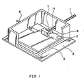
- Fig. 1 is a perspective view of a major part of the optical module according to one embodiment of this invention;
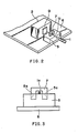
- Fig. 2 is a partial perspective view of the embodiment of Fig. 1 for explaining fixation of an optical fiber;
- Fig. 3 is a front view of the embodiment of Fig. 1;
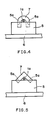
- Figs. 4 and 5 are front views of modifications of the pre-formed structure other than those respectively shown in Figs. 2 and 3.
- In an optical receiving module according to one embodiment of present invention, as shown in Fig. 1, in a metal package 3 there is provided a hybrid integrated circuit (IC)
substrate 6 having a required circuit not shown. Openings are formed in side walls of the package 3. Through the openings an electric signal line 8 and an optical fiber 1 are inserted in the package 3. - The optical fiber 1 is optically connected to a pin-photodiode not shown provided on a side of a
carrier chip 2, and a light emitted from the end of the optical fiber 1 is incident on the light receiving portion of the pin-photodiode as a light receiving device. - The optical fiber 1 has the end 1a made of the so called metallized fiber which comprises exposed glass fiber and a plating applied thereto. The end 1a of the optical fiber 1 is first positioned precisely on a
fiber saddle 5 disposed near thecarrier chip 2 and then soldered to thefiber saddle 5. - The
hybrid IC substrate 6 is made of a heat insulative material, e.g., ceramics or others. Thecarrier chip 2 is mounted on thehybrid IC chip 6 as one element of the circuit. Thefiber saddle 5 is made of metal or ceramics vacuum evaporated with metal and is beforehand plated with a solder. Thefiber saddle 5 is die bonded to thehybrid IC substrate 6 with a solder having a relatively high melting point, e.g., gold and tin (Au-Sn} solder with a melting point of 280°C. - After a cream solder is applied around the
fiber saddle 5, thefiber saddle 5 is mounted on thehybrid IC substrate 6 and then heated. It is possible that the plating and die bonding of thefiber saddle 5 are performed simultaneously. - Next, the fixation of the end 1a of the optical fiber 1 to the
fiber saddle 5 will be explained with reference to Figs. 2 and 3. - The end 1a of the optical fiber 1 is positioned so as to be optically connected to the pin-photodiode 9 on the front side wall of the
carrier chip 2.Concavities 5a are formed on the top of thefiber saddle 5. In theconcavities 5a are inserted the legs of apre-formed structure 7 bridged over the end 1a of the optical fiber 1 positioned on the top of thefiber saddle 5. Thepreformed structure 7 is made of a solder containing no flux and is shaped in a square bracket. It is preferable that the solder of thepre-formed structure 7 has lower melting point than that used to die bond thefiber saddle 5. The end 1a of the optical fiber 1 is plated beforehand into a metallized fiber so as to be convenient for the soldering. - The
pre-formed structure 7 and thefiber saddle 5 as arranged in the above described manner are heated. When the heating temperature becomes above the melting point of thepre-formed structure 7, thepre-formed structure 7 melts. Then the heating is stopped. The meltedpreformed structure 7 cools and solidifies, and the end 1a of the optical fiber 1 is fixed to thefiber saddle 5. - The end 1a of the optical fiber 1 may be positioned on the top of the
fiber saddle 5 after the legs of thepre-formed structure 7 is inserted fixedly in theconcavities 5a and then the end 1a of the optical fiber 1 is put into the gap between thepre-formed structure 7 and thefiber saddle 5. - In this embodiment, the
pre-formed structure 7 has a square bracket shape before melted but may have a U-shape or an L-shape as shown in Figs. 4 and 5. - Finally, a top cover not shown is attached to the package for close sealing, and the optical module is completed.
- In this embodiment, two legs of the
pre-formed structure 7 are inserted in theconcavities 5a respectively. But the pre-formed structure may have a J-shape in which the two legs have different lengths, and only one of the two legs is inserted in theconcavity 5a. In thiscase rhe concavity 5a may be one. And fiber saddle may not have cocavities. In this case the pre-formed structure can be placed on the fixation surface to be bridged over the optical fiber positioned on the fixation surface. - This embodiment is a receiving optical module comprising a pin-photodiode as a light receiving device, and an optical fiber optically connected to the light receiving device. But the optical module according to this invention can be a transmitting optical module by replacing the light receiving device with a light emitting diode or a laser diode as a light emitting device.
- From the invention thus described, it will be obvious that the invention may be varied in many ways. Such variations are not to be regarded as a departure from the spirit and scope of the invention, and all such modifications as would be obvious to one skilled in the art are intended to be included within the scope of the following claims.
Claims (10)
a package (3) housing an optically operative device (2); an optical fiber (1) whose end (1a) is inserted in the package (3) and optically connected to the optically operative device (2); and
a fiber saddle (5) for fixing the optical fiber (1) characterized in that
the fiber saddle (5) is mounted on a heat insulative substrate (6).
an optically operative device (2) to be optically connected to an optical fiber (1); and
a fiber saddle (5) which the optical fiber (1) is fixed to and is provided near the optically operative device (2) the optical fiber (1) being fixed to the fiber saddle (5) by solder,
characterized in that,
the fixation of the optical fiber (1) to the fiber saddle (5) being performed by melt and solidification of a preformed structure (7) made of solder and bridged over the optical fiber (1) positioned on the fiber saddle (5).
- plating the fixation surface of the fiber saddle with solder
- positioning the optical fiber to the fiber saddle
- positioning a pre-formed structure made of solder over the optical fiber
- melting and solidifying the pre-formed structure.
Applications Claiming Priority (4)
| Application Number | Priority Date | Filing Date | Title |
|---|---|---|---|
| JP10092888A JPH01270013A (en) | 1988-04-22 | 1988-04-22 | Optical module |
| JP10092788A JPH01270012A (en) | 1988-04-22 | 1988-04-22 | Optical module |
| JP100928/88 | 1988-04-22 | ||
| JP100927/88 | 1988-04-22 |
Publications (3)
| Publication Number | Publication Date |
|---|---|
| EP0346596A2 true EP0346596A2 (en) | 1989-12-20 |
| EP0346596A3 EP0346596A3 (en) | 1990-06-13 |
| EP0346596B1 EP0346596B1 (en) | 1994-01-12 |
Family
ID=26441867
Family Applications (1)
| Application Number | Title | Priority Date | Filing Date |
|---|---|---|---|
| EP89107185A Expired - Lifetime EP0346596B1 (en) | 1988-04-22 | 1989-04-21 | Optical module with connected optical fiber |
Country Status (4)
| Country | Link |
|---|---|
| US (1) | US4955683A (en) |
| EP (1) | EP0346596B1 (en) |
| CA (1) | CA1323227C (en) |
| DE (1) | DE68912206T2 (en) |
Cited By (5)
| Publication number | Priority date | Publication date | Assignee | Title |
|---|---|---|---|---|
| EP0511931A2 (en) * | 1991-04-29 | 1992-11-04 | International Business Machines Corporation | An apparatus and a method for an optical fiber interface |
| US5241614A (en) * | 1991-04-29 | 1993-08-31 | International Business Machines Corporation | Apparatus and a method for an optical fiber interface |
| EP0717297A2 (en) * | 1994-12-12 | 1996-06-19 | Nortel Networks Corporation | Optically coupling optical fibres to injection lasers |
| US7263260B2 (en) | 2005-03-14 | 2007-08-28 | Matsushita Electric Industrial Co., Ltd. | Low cost, high precision multi-point optical component attachment |
| US7410088B2 (en) * | 2003-09-05 | 2008-08-12 | Matsushita Electric Industrial, Co., Ltd. | Solder preform for low heat stress laser solder attachment |
Families Citing this family (10)
| Publication number | Priority date | Publication date | Assignee | Title |
|---|---|---|---|---|
| US5553182A (en) * | 1995-02-14 | 1996-09-03 | Mcdonnell Douglas Corporation | Alignment fixture and associated method for controllably positioning on optical fiber |
| US5606635A (en) * | 1995-06-07 | 1997-02-25 | Mcdonnell Douglas Corporation | Fiber optic connector having at least one microactuator for precisely aligning an optical fiber and an associated fabrication method |
| US5602955A (en) * | 1995-06-07 | 1997-02-11 | Mcdonnell Douglas Corporation | Microactuator for precisely aligning an optical fiber and an associated fabrication method |
| WO1998012587A1 (en) * | 1995-06-07 | 1998-03-26 | Mcdonnell Douglas Corporation | An alignment apparatus for precisely aligning an optical fiber and an associated fabrication method |
| JPH10190141A (en) * | 1996-12-20 | 1998-07-21 | Fujitsu Ltd | Optical semiconductor module |
| US6679636B1 (en) | 2001-06-29 | 2004-01-20 | Network Elements, Inc. | Method and apparatus for maintaining alignment of a laser diode with an optical fiber |
| US6671975B2 (en) | 2001-12-10 | 2004-01-06 | C. William Hennessey | Parallel kinematic micromanipulator |
| DE102008011525A1 (en) | 2008-02-27 | 2009-09-10 | Jenoptik Laserdiode Gmbh | Method for producing a light transmission arrangement and light transmission arrangement |
| JP5509317B2 (en) | 2010-03-30 | 2014-06-04 | 株式会社フジクラ | Laser apparatus and manufacturing method thereof |
| US20140328039A1 (en) * | 2011-09-26 | 2014-11-06 | Alpha Metals, Inc. | Systems and methods for void reduction in a solder joint |
Citations (4)
| Publication number | Priority date | Publication date | Assignee | Title |
|---|---|---|---|---|
| GB2065918A (en) * | 1979-12-17 | 1981-07-01 | Western Electric Co | Coupling optical device |
| FR2582413A1 (en) * | 1985-05-23 | 1986-11-28 | Comp Generale Electricite | Method for coupling an optical fibre to an optoelectronic component on a base |
| JPS62115405A (en) * | 1985-11-15 | 1987-05-27 | Fujitsu Ltd | Optical coupler |
| EP0264335A1 (en) * | 1986-10-17 | 1988-04-20 | Thomson Hybrides Et Microondes | Coupling module for a semiconductor laser with an optical fibre, and alignment method for this semiconductor device and this fibre |
Family Cites Families (6)
| Publication number | Priority date | Publication date | Assignee | Title |
|---|---|---|---|---|
| JPS53128991A (en) * | 1977-04-15 | 1978-11-10 | Nec Corp | Coupler for optical semiconductor parts |
| FR2503458A1 (en) * | 1981-04-02 | 1982-10-08 | Cit Alcatel | Optical head mfg. process for electroluminescent device - has unitary construction with U=shaped tin diffusion on substrate with stems holding fibre and device respectively |
| FR2547661B1 (en) * | 1983-06-14 | 1986-10-24 | Telecommunications Sa | METHOD AND DEVICE FOR CONNECTING AN OPTICAL FIBER WITH A PHOTOSENSITIVE DETECTOR AND THE METHOD OF IMPLEMENTING |
| JPS6173206A (en) * | 1984-09-18 | 1986-04-15 | Hitachi Maxell Ltd | Magnetic recording and reproducing system |
| JPS61173205A (en) * | 1985-01-29 | 1986-08-04 | Fujitsu Ltd | Fixing method of optical coupling part |
| US4722586A (en) * | 1985-04-12 | 1988-02-02 | Tektronix, Inc. | Electro-optical transducer module |
-
1989
- 1989-04-18 US US07/339,799 patent/US4955683A/en not_active Expired - Fee Related
- 1989-04-20 CA CA000597280A patent/CA1323227C/en not_active Expired - Fee Related
- 1989-04-21 DE DE68912206T patent/DE68912206T2/en not_active Expired - Fee Related
- 1989-04-21 EP EP89107185A patent/EP0346596B1/en not_active Expired - Lifetime
Patent Citations (4)
| Publication number | Priority date | Publication date | Assignee | Title |
|---|---|---|---|---|
| GB2065918A (en) * | 1979-12-17 | 1981-07-01 | Western Electric Co | Coupling optical device |
| FR2582413A1 (en) * | 1985-05-23 | 1986-11-28 | Comp Generale Electricite | Method for coupling an optical fibre to an optoelectronic component on a base |
| JPS62115405A (en) * | 1985-11-15 | 1987-05-27 | Fujitsu Ltd | Optical coupler |
| EP0264335A1 (en) * | 1986-10-17 | 1988-04-20 | Thomson Hybrides Et Microondes | Coupling module for a semiconductor laser with an optical fibre, and alignment method for this semiconductor device and this fibre |
Non-Patent Citations (2)
| Title |
|---|
| PATENT ABSTRACTS OF JAPAN. vol. 11, no. 334 (P-631) 31 Oktober 1987; & JP-A-62 115 405 (FUJITSU LTD.) 27-05-1987 * |
| PATENT ABSTRACTS OF JAPAN. vol. 12, no. 69 (E-587) 3 March 1988; & JP-A-62 211 965 (TOSHIBA CORP.) 17-09-1987 * |
Cited By (7)
| Publication number | Priority date | Publication date | Assignee | Title |
|---|---|---|---|---|
| EP0511931A2 (en) * | 1991-04-29 | 1992-11-04 | International Business Machines Corporation | An apparatus and a method for an optical fiber interface |
| EP0511931A3 (en) * | 1991-04-29 | 1993-03-31 | International Business Machines Corporation | An apparatus and a method for an optical fiber interface |
| US5241614A (en) * | 1991-04-29 | 1993-08-31 | International Business Machines Corporation | Apparatus and a method for an optical fiber interface |
| EP0717297A2 (en) * | 1994-12-12 | 1996-06-19 | Nortel Networks Corporation | Optically coupling optical fibres to injection lasers |
| EP0717297A3 (en) * | 1994-12-12 | 1996-11-27 | Northern Telecom Ltd | Optically coupling optical fibres to injection lasers |
| US7410088B2 (en) * | 2003-09-05 | 2008-08-12 | Matsushita Electric Industrial, Co., Ltd. | Solder preform for low heat stress laser solder attachment |
| US7263260B2 (en) | 2005-03-14 | 2007-08-28 | Matsushita Electric Industrial Co., Ltd. | Low cost, high precision multi-point optical component attachment |
Also Published As
| Publication number | Publication date |
|---|---|
| EP0346596B1 (en) | 1994-01-12 |
| DE68912206T2 (en) | 1994-08-04 |
| CA1323227C (en) | 1993-10-19 |
| US4955683A (en) | 1990-09-11 |
| DE68912206D1 (en) | 1994-02-24 |
| EP0346596A3 (en) | 1990-06-13 |
Similar Documents
| Publication | Publication Date | Title |
|---|---|---|
| EP0346596A2 (en) | Optical module with connected optical fiber | |
| US5647042A (en) | Optical link module connection system | |
| US5519720A (en) | Semiconductor light emitting device | |
| US6318910B1 (en) | Method for hermetically sealing optical fiber introducing section and hermetically sealed structure | |
| US4722586A (en) | Electro-optical transducer module | |
| EP0100086A2 (en) | A Method of making injection laser packages and packages made by using the method | |
| US20050201666A1 (en) | Optical module, manufacturing method therefor, protective component, and protective component with electric wiring | |
| JP2003528440A (en) | Method and apparatus for sealing an electronic package | |
| EP0765490A2 (en) | Optical miniature capsule | |
| US7841781B2 (en) | Methods and apparatuses for providing a hermetic sealing system for an optical transceiver module | |
| EP0824281B1 (en) | Peltier cooler and use in a semiconductor laser module | |
| EP0439227A1 (en) | Semiconductor device comprising a support, method of manufacturing it, and method of manufacturing the support | |
| EP0477841B1 (en) | Laser diode module and method for fabricating the same | |
| US6565267B2 (en) | Optical transmitting device and optical receiving device each having receptacle type optical module | |
| AU607005B2 (en) | An opto-electronic device | |
| US5028111A (en) | Method of fixing cylindrical optical part and electric part | |
| US20040179793A1 (en) | Optoelectronic device packaging assemblies and methods of making the same | |
| EP1570306B1 (en) | Method for forming an attachment to an optical fiber and optical fiber attachment | |
| CA1151277A (en) | Method of anchoring optical fiber in the hermetic laser package | |
| EP0548882A1 (en) | Hybrid optical/electrical circuit module | |
| JP2002521847A (en) | Optoelectronic device lead frame attachment | |
| JPH01270012A (en) | Optical module | |
| US5200612A (en) | Photodetector carrier for improving the high speed of a photodetector and method for producing same | |
| JPH01302214A (en) | Chip carrier | |
| JP2513134B2 (en) | Chip on carrier |
Legal Events
| Date | Code | Title | Description |
|---|---|---|---|
| PUAI | Public reference made under article 153(3) epc to a published international application that has entered the european phase |
Free format text: ORIGINAL CODE: 0009012 |
|
| AK | Designated contracting states |
Kind code of ref document: A2 Designated state(s): DE FR GB SE |
|
| PUAL | Search report despatched |
Free format text: ORIGINAL CODE: 0009013 |
|
| AK | Designated contracting states |
Kind code of ref document: A3 Designated state(s): DE FR GB SE |
|
| 17P | Request for examination filed |
Effective date: 19901213 |
|
| 17Q | First examination report despatched |
Effective date: 19920630 |
|
| GRAA | (expected) grant |
Free format text: ORIGINAL CODE: 0009210 |
|
| AK | Designated contracting states |
Kind code of ref document: B1 Designated state(s): DE FR GB SE |
|
| REF | Corresponds to: |
Ref document number: 68912206 Country of ref document: DE Date of ref document: 19940224 |
|
| ET | Fr: translation filed | ||
| PLBE | No opposition filed within time limit |
Free format text: ORIGINAL CODE: 0009261 |
|
| STAA | Information on the status of an ep patent application or granted ep patent |
Free format text: STATUS: NO OPPOSITION FILED WITHIN TIME LIMIT |
|
| 26N | No opposition filed | ||
| EAL | Se: european patent in force in sweden |
Ref document number: 89107185.4 |
|
| PGFP | Annual fee paid to national office [announced via postgrant information from national office to epo] |
Ref country code: FR Payment date: 19960410 Year of fee payment: 8 |
|
| PGFP | Annual fee paid to national office [announced via postgrant information from national office to epo] |
Ref country code: GB Payment date: 19960412 Year of fee payment: 8 |
|
| PGFP | Annual fee paid to national office [announced via postgrant information from national office to epo] |
Ref country code: SE Payment date: 19960417 Year of fee payment: 8 |
|
| PGFP | Annual fee paid to national office [announced via postgrant information from national office to epo] |
Ref country code: DE Payment date: 19960429 Year of fee payment: 8 |
|
| PG25 | Lapsed in a contracting state [announced via postgrant information from national office to epo] |
Ref country code: GB Effective date: 19970421 |
|
| PG25 | Lapsed in a contracting state [announced via postgrant information from national office to epo] |
Ref country code: SE Effective date: 19970422 |
|
| GBPC | Gb: european patent ceased through non-payment of renewal fee |
Effective date: 19970421 |
|
| PG25 | Lapsed in a contracting state [announced via postgrant information from national office to epo] |
Ref country code: FR Free format text: LAPSE BECAUSE OF NON-PAYMENT OF DUE FEES Effective date: 19971231 |
|
| PG25 | Lapsed in a contracting state [announced via postgrant information from national office to epo] |
Ref country code: DE Free format text: LAPSE BECAUSE OF NON-PAYMENT OF DUE FEES Effective date: 19980101 |
|
| EUG | Se: european patent has lapsed |
Ref document number: 89107185.4 |
|
| REG | Reference to a national code |
Ref country code: FR Ref legal event code: ST |