EP0341122A1 - Matrix charge transfer photodetector having an integrated charge filtering device - Google Patents
Matrix charge transfer photodetector having an integrated charge filtering device Download PDFInfo
- Publication number
- EP0341122A1 EP0341122A1 EP89401129A EP89401129A EP0341122A1 EP 0341122 A1 EP0341122 A1 EP 0341122A1 EP 89401129 A EP89401129 A EP 89401129A EP 89401129 A EP89401129 A EP 89401129A EP 0341122 A1 EP0341122 A1 EP 0341122A1
- Authority
- EP
- European Patent Office
- Prior art keywords
- zone
- transfer
- auxiliary
- low
- type
- Prior art date
- Legal status (The legal status is an assumption and is not a legal conclusion. Google has not performed a legal analysis and makes no representation as to the accuracy of the status listed.)
- Withdrawn
Links
- 239000011159 matrix material Substances 0.000 title claims abstract description 20
- 238000001914 filtration Methods 0.000 title claims abstract description 17
- 239000000758 substrate Substances 0.000 claims abstract description 23
- 101150101414 PRP1 gene Proteins 0.000 claims abstract description 3
- 101100368710 Rattus norvegicus Tacstd2 gene Proteins 0.000 claims abstract description 3
- 101100342406 Saccharomyces cerevisiae (strain ATCC 204508 / S288c) PRS1 gene Proteins 0.000 claims abstract description 3
- 230000005855 radiation Effects 0.000 claims description 6
- 239000004065 semiconductor Substances 0.000 claims description 3
- 101000951145 Homo sapiens Succinate dehydrogenase [ubiquinone] cytochrome b small subunit, mitochondrial Proteins 0.000 claims 1
- 102100038014 Succinate dehydrogenase [ubiquinone] cytochrome b small subunit, mitochondrial Human genes 0.000 claims 1
- 230000007704 transition Effects 0.000 abstract description 4
- 239000012535 impurity Substances 0.000 description 9
- 238000010586 diagram Methods 0.000 description 6
- 230000009471 action Effects 0.000 description 5
- 239000000470 constituent Substances 0.000 description 5
- 230000006870 function Effects 0.000 description 5
- 238000009792 diffusion process Methods 0.000 description 4
- 238000000034 method Methods 0.000 description 4
- 230000010354 integration Effects 0.000 description 3
- VYPSYNLAJGMNEJ-UHFFFAOYSA-N Silicium dioxide Chemical compound O=[Si]=O VYPSYNLAJGMNEJ-UHFFFAOYSA-N 0.000 description 2
- XUIMIQQOPSSXEZ-UHFFFAOYSA-N Silicon Chemical compound [Si] XUIMIQQOPSSXEZ-UHFFFAOYSA-N 0.000 description 2
- 230000008859 change Effects 0.000 description 2
- 238000002513 implantation Methods 0.000 description 2
- 229910052710 silicon Inorganic materials 0.000 description 2
- 239000010703 silicon Substances 0.000 description 2
- 229910052814 silicon oxide Inorganic materials 0.000 description 2
- 241001644893 Entandrophragma utile Species 0.000 description 1
- 238000009825 accumulation Methods 0.000 description 1
- 239000003990 capacitor Substances 0.000 description 1
- 230000008878 coupling Effects 0.000 description 1
- 238000010168 coupling process Methods 0.000 description 1
- 238000005859 coupling reaction Methods 0.000 description 1
- 238000005286 illumination Methods 0.000 description 1
- 238000004519 manufacturing process Methods 0.000 description 1
- 238000005036 potential barrier Methods 0.000 description 1
- 230000008569 process Effects 0.000 description 1
- 230000009467 reduction Effects 0.000 description 1
Images


Classifications
-
- H—ELECTRICITY
- H04—ELECTRIC COMMUNICATION TECHNIQUE
- H04N—PICTORIAL COMMUNICATION, e.g. TELEVISION
- H04N3/00—Scanning details of television systems; Combination thereof with generation of supply voltages
- H04N3/10—Scanning details of television systems; Combination thereof with generation of supply voltages by means not exclusively optical-mechanical
- H04N3/14—Scanning details of television systems; Combination thereof with generation of supply voltages by means not exclusively optical-mechanical by means of electrically scanned solid-state devices
- H04N3/15—Scanning details of television systems; Combination thereof with generation of supply voltages by means not exclusively optical-mechanical by means of electrically scanned solid-state devices for picture signal generation
- H04N3/155—Control of the image-sensor operation, e.g. image processing within the image-sensor
- H04N3/1568—Control of the image-sensor operation, e.g. image processing within the image-sensor for disturbance correction or prevention within the image-sensor, e.g. biasing, blooming, smearing
-
- H—ELECTRICITY
- H01—ELECTRIC ELEMENTS
- H01L—SEMICONDUCTOR DEVICES NOT COVERED BY CLASS H10
- H01L27/00—Devices consisting of a plurality of semiconductor or other solid-state components formed in or on a common substrate
- H01L27/14—Devices consisting of a plurality of semiconductor or other solid-state components formed in or on a common substrate including semiconductor components sensitive to infrared radiation, light, electromagnetic radiation of shorter wavelength or corpuscular radiation and specially adapted either for the conversion of the energy of such radiation into electrical energy or for the control of electrical energy by such radiation
- H01L27/144—Devices controlled by radiation
- H01L27/146—Imager structures
- H01L27/148—Charge coupled imagers
- H01L27/14831—Area CCD imagers
-
- H—ELECTRICITY
- H04—ELECTRIC COMMUNICATION TECHNIQUE
- H04N—PICTORIAL COMMUNICATION, e.g. TELEVISION
- H04N25/00—Circuitry of solid-state image sensors [SSIS]; Control thereof
- H04N25/40—Extracting pixel data from image sensors by controlling scanning circuits, e.g. by modifying the number of pixels sampled or to be sampled
- H04N25/44—Extracting pixel data from image sensors by controlling scanning circuits, e.g. by modifying the number of pixels sampled or to be sampled by partially reading an SSIS array
- H04N25/443—Extracting pixel data from image sensors by controlling scanning circuits, e.g. by modifying the number of pixels sampled or to be sampled by partially reading an SSIS array by reading pixels from selected 2D regions of the array, e.g. for windowing or digital zooming
-
- H—ELECTRICITY
- H04—ELECTRIC COMMUNICATION TECHNIQUE
- H04N—PICTORIAL COMMUNICATION, e.g. TELEVISION
- H04N25/00—Circuitry of solid-state image sensors [SSIS]; Control thereof
- H04N25/60—Noise processing, e.g. detecting, correcting, reducing or removing noise
- H04N25/62—Detection or reduction of noise due to excess charges produced by the exposure, e.g. smear, blooming, ghost image, crosstalk or leakage between pixels
- H04N25/621—Detection or reduction of noise due to excess charges produced by the exposure, e.g. smear, blooming, ghost image, crosstalk or leakage between pixels for the control of blooming
-
- H—ELECTRICITY
- H04—ELECTRIC COMMUNICATION TECHNIQUE
- H04N—PICTORIAL COMMUNICATION, e.g. TELEVISION
- H04N25/00—Circuitry of solid-state image sensors [SSIS]; Control thereof
- H04N25/70—SSIS architectures; Circuits associated therewith
- H04N25/71—Charge-coupled device [CCD] sensors; Charge-transfer registers specially adapted for CCD sensors
- H04N25/72—Charge-coupled device [CCD] sensors; Charge-transfer registers specially adapted for CCD sensors using frame transfer [FT]
Definitions
- the invention relates to matrix photodetectors with charge transfer of the type comprising filtering means for outputting only payloads corresponding to a useful portion of incident light radiation.
- Photodetectors are used in principle to store, transfer and deliver loads as a function of the incident light radiation to which they are subjected, in order to restore a digital image.
- the photodetectors a distinction is made between those which generally have a single row (or strip) of photosensitive elements and those, surface or matrix, organized either in frame transfer or in interline transfer and which are constituted by sets of channels of parallel load transfer.
- the invention relates only to matrix photodetectors.
- FIG. 1 schematically represents a conventional matrix photodetector organized in frame transfer.
- This photodetector 1 comprises a first zone 1 comprising a photosensitive sub-zone 10, commonly called the image zone and a non-photosensitive sub-zone 11, commonly called the memory zone.
- the photodetector 1 also includes a second zone 2 connected to the first zone 1 comprising a read register 20, extended by a read diode 21 connected to a control transistor 22.
- the image area 10 is a matrix comprising n rows and p columns. Each column is a vertical charge transfer shift register constituting a charge transfer channel.
- the register boxes are photo sensitive and charges accumulate there depending on the illumination of the hut.
- the memory zone is constituted in an identical manner to the image zone but but the boxes of the various registers are not photosensitive.
- the read register is a horizontal shift register.
- the image and memory areas also include transfer grids surmounting the transfer channels and suitable for receiving low or high control signals to apply a low or high potential level to the transfer channels so as to allow charge transfer there.
- the read register is suitable for receiving at least part of the charges stored in the memory area and is surmounted by a read grid suitable for also receiving low or high control signals to apply a low potential level to the read register. or high, so as to allow the transfer of the charges contained in this read register into the read diode.
- FIG. 2 schematically illustrates a matrix photodetector organized in interline transfer.
- the image area 10 ′ is constituted by columns of photodiodes interconnected with columns of photosensitive cells belonging to vertical shift registers constituting the memory area 11 ′.
- the lower part of each transfer channel CT ′ is connected to a box of a horizontal shift register constituting the read register 20 ′.
- the operating principle of a photodetector organized in interline transfer is substantially similar.
- the charges stored in the photodiodes are transferred horizontally to the shift registers then each line of the shift registers is shifted vertically in the reading register and transferred to the reading medium by a horizontal shift of the latter.
- FIGS. 3A to 3C schematically illustrate a filtering principle currently used in the state of the art for outputting only payloads corresponding to said useful portion IMD of the incident light radiation IM, that is to say to the portion of the image you want to view.
- Figure 3A shows the desired image IMD.
- the total image IM including the desired image IMD, is shown already transferred in the memory area 11.
- SCM control signal
- control signal SCL under the action of the control signal SCL, low or high, applied to the reading grid, transfers the line it contains into the reading diode.
- This line is then, effectively or not, output at the control of the filtering control signal SCF which is, in fact, a control clock of the gate of the control transistor.
- SCF filtering control signal
- the control signal SCF exhibits a change of state (up / down or the reverse) during the action of control signal SCL
- the line present in the read register is effectively transferred into the read diode then output, while, when the SCF control signal is high, the read diode is reset to 0 and no line is delivered.
- the control transistor 22 and the control signal SCF therefore form part of the filtering means.
- FIG. 3C A timing diagram of the image restitution, present in the memory area, is illustrated in FIG. 3C.
- the reading register is assumed to have only one line.
- the first i pulses of the control signal SCM the first i lines of the image IM are successively transferred to the read register 2. This, under the action of the first i pulses of the control signal SCL, releases these lines.
- the control signal SCF being meanwhile constantly high, none of these lines is actually delivered at the output of the photodetector. We therefore eliminated unnecessary charges corresponding to lines 1 to i of the image.
- the present invention overcomes these drawbacks by proposing a matrix photodetector provided with means for filtering the payloads which do not require oversizing of the reading register and allowing a very high image scanning rate.
- the subject of the invention is therefore a matrix photodetector charge transfer of the type comprising: a first zone, partly photosensitive, in which said charges are stored and comprising, on a semiconductor substrate: . a plurality of parallel charge transfer channels, . transfer grids surmounting the transfer channels and suitable for receiving low or high control signals to apply a low or high potential level to the transfer channels, so as to allow charge transfer there, a second zone, connected to the first zone, capable of receiving at least a portion of the charges stored in the first zone, and comprising . a read register extended by a read diode, .
- a reading grid surmounting the reading register and suitable for receiving low or high control signals to apply a low or high potential level to the reading register, so as to allow the transfer of the charges contained in the reading register into the reading diode, and, .
- filtering means acting on the reading diode so as to deliver only payloads at the output corresponding to a useful portion of the incident light radiation, characterized in that the filtering means comprise, in the first zone, an auxiliary zone comprising an implanted region of a type opposite to that of the substrate, parallel to the transfer channels and followed by a region passage of charges, located in the extension of the transfer channels, and surmounted by an auxiliary grid suitable for receiving low or high control auxiliary signals, to apply to the passage region low or high auxiliary potential levels, respectively in absolute value below the low or high potential levels produced by the other grids, which allows a first filtering of the charges before their transfer to the reading register.
- the auxiliary zone comprises an anti-dazzle device of the type with an insulating zone, that is to say of the type described in French Patent Application No. 82-11395, in the name of the Applicant.
- the passage region comprises an implanted portion of type identical to that of the substrate and the low or high control signals are then respectively identical in amplitude to the low or high control signals of the other grids.
- the low or high auxiliary control signals have different amplitudes from the respective ones of the other low or high control signals.
- the photodetector is of the frame transfer type and the auxiliary zone is located at the bottom of the image zone.
- the photodetector is of the frame transfer type and the auxiliary area is located at the end of the memory area.
- the photodetector can also be of the interline transfer type and the auxiliary zone is then located at the bottom of the memory zone.
- the photodetector according to the invention can be equipped with at least one other anti-dazzle device of the type with an insulating zone situated in the photosensitive part of the first zone.
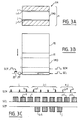
- FIG. 4 schematically represents a first embodiment of the photodetector according to the invention.
- the photodetector is of the raster transfer matrix type and it can be seen that the image area 10 comprises n + 1 lines, one line more than in a conventional photodetector of the prior art.
- the nth line of the image zone that is to say the penultimate line, comprises implanted regions of type opposite to that of the substrate, parallel to the transfer channels. These implanted regions, as well as the additional line n + 1, form part of an auxiliary zone 100 which will be detailed below, and which is therefore located at the bottom of the image zone.
- FIG. 5 schematically represents a second embodiment of the frame transfer matrix photodetector.
- the memory area 11 comprises n ⁇ 1 lines, that is to say one line more than in a prior art photodetector.
- the auxiliary area 110 is analogous to the auxiliary area 100 and is located on the lines n and n + 1 of the memory area 11, respectively referenced 11d and 11g, that is to say at the bottom of the memory area.
- FIG. 6 schematically represents a third embodiment of a photodetector according to the invention in the case where it is of the interline transfer type.
- the transfer channels CT ′ of the memory area 11 ′ comprise n + 1 boxes, and an auxiliary area 110 ′ similar to the auxiliary areas 100 and 110 is defined, located at the bottom of the memory area.
- FIGS. 7 to 10 describe, in detail, the structure of an auxiliary zone 110, located at the bottom of the memory zone 11, in the case of a matrix photodetector with frame transfer.
- FIGS. 7 to 10 therefore show more precisely the lines n-1, n and n + 1 of the memory area 11, respectively referenced 11a, 11d and 11g.
- the charge transfer photodetector comprises a semiconductor substrate S such as P-type silicon, for example, covered at least in part with an insulating layer 40, made for example of silicon oxide.
- a transfer channel CT has been shown in which the charges are capable of being transferred longitudinally in the direction of the arrow F.
- Each of the lines of the matrix photodetector comprises transfer grids such as GTa and GTd, covering the transfer channel CT and arranged substantially perpendicular to the direction of the charge transfer.
- the assembly (grid - insulating layer - substrate) defines in the CT transfer channel capacitors of the type with charge coupling.
- the transfer channel portion located on line 11d, includes an anti-dazzle device of the type described in French Patent Application No. 82-11395.
- This anti-glare device will be designated subsequently under the name "anti-glare device of the type with insulating zone”.
- the main constituent elements as well as the main operating principles will be recalled below, those skilled in the art can refer to the above-mentioned French Patent Application No. 82-11395 for more details.
- the CT transfer channel comprises, in the case where the charge is transferred in volume, an implantation of impurities 50 of a type opposite to that of the substrate which occupies the entire width of this CT channel.
- the insulating zone type anti-dazzle device is located between two adjacent transfer channels. This device comprises a diode D formed by an implanted region of the type opposite to that of the substrate, that is to say of the N type and parallel to the transfer channel CT. This device also includes a transition zone ZT ensuring a reduction in the surface potential of the substrate, the surface potential of this transition zone ZT varying as a function of the potential applied to the grid GTd.
- the diode D and the transfer zone ZT are surrounded on all sides, with the exception of that contiguous to the transfer channel CT, by an insulating zone ZI, such as the surface potential in the substrate, under this insulating zone, ie null and invariable as a function of the voltages applied to the GTd grids as well as to the adjacent grids.
- this insulating zone ZI can be produced by implanting impurities of the same type as that of the substrate with a higher concentration of impurities. at 1019 atoms / cm3, or by an insulating deposit such as silicon oxide under a thickness of approximately 1 micron.
- This insulating zone ZI extends on line 11a to be contiguous to the portion of transfer channel CT covered with the grid GTa.
- the additional line 11g comprises a portion of transfer channel having between the diffusion of impurities 50 and the insulating zone 40 a diffusion of impurities 60 of the type opposite to the diffusion of impurities 50, therefore of the same type as that of the substrate, that is to say of the P type.
- This transfer channel portion constitutes a passage region RP for the charges passing from the memory area 11 to the read register 20.
- This transfer region RP therefore extends the channel CT in the memory area 11.
- Line 11g also includes the extension of the insulating area ZI parallel to the passage region RP.
- the auxiliary zone 110 includes the anti-dazzle device of the insulating zone type comprising the diode D, the transition zone ZT and the insulating zone ZI, as well as the passage region RP covered with an auxiliary grid GA of the same type as the transfer grids GTa and GTd.
- This auxiliary grid GA is controlled independently of the other transfer grids and of the reading grid GL.
- FIGS. 8A to 10A illustrate, schematically, the evolution of the surface potentials PS of the different regions of the substrate.
- each grid is controlled by a low or high control signal which gives the area located under the grid a low or high potential level.
- the reference of the potential level of an area will be assigned the suffix 0 for a low potential level and the suffix 1 for a high potential level. So the low potential level of the serving transfer channel, located under the GTa transfer grid, will be assigned the reference PGa0.
- FIGS. 8A, 9A and 10A show that the surface potential PZI, in the insulating zone ZI, is zero and invariable as a function of the potentials applied to the different grids.
- the first part of FIG. 9A shows the evolution of the surface potential PS when the transfer gate GTd is activated by the low control signal and the second part of this same figure 9A shows the evolution of the surface potentials when the gate transfer signal GTd is activated by the control signal O. In the latter case, when there is charge accumulation and exceeding the anti-glare level NAE, there is evacuation of excess charges towards the potential well formed by the diode D.
- the level of the high potential PZT1, of the transfer zone must be higher than the level of low potential PGd0, so that the charges in excess go preferably towards the diode D instead of overflowing in the direction of transfer to other potential wells.
- FIG. 10A illustrates the evolution of the surface potential under the auxiliary grid GA, the latter being subjected to a low or high auxiliary control signal.
- the auxiliary control signals of the auxiliary grid GA are identical in amplitude to the control signals of the transfer and reading grids, but the compensation caused by the diffusion of the impurity zone 60 causes a PRP potential level in the RP passage area different from the potential levels in the rest of the transfer channel.
- the surface potential PRP0 of the passage region is lower than the potential PGd0 and when the auxiliary gate is activated by the auxiliary control signal in the high state, the high potential level PRP1 of the passage region is lower than the potential levels PGd1 but higher than the anti-dazzle level NAE.
- FIG. 11 schematically illustrates a longitudinal section of the lines 11a, 11d and 11g as well as of the reading register 20, this section showing the implantation of impurities 60 of the same type as the substrate.
- FIG. 11A shows the evolution of the surface potential corresponding to the section of FIG. 11, in a particular case of operation. It is assumed, in this case, that the transfer gate GTa is activated by the control signal in the low state, that the transfer gate GTd is activated by the control signal in the high state, as well as for the reading grid GL, while the auxiliary grid is activated by the auxiliary control signal in the low state.
- FIG. 11A therefore shows the positioning of the different potential levels with respect to each other.
- the auxiliary control signals of the auxiliary grid GA can be different in amplitude with respect to the control signals of the other grids, so as to apply to the auxiliary grid a voltage lower than that of the other grids to respect the scale of potential levels.
- FIGS. 11A and 12 will now serve to illustrate the operating principle of the photodetector according to the invention.
- the reference SCM designates the control signal applied to the different transfer grids of the memory area
- the reference SCL designates the control signal applied to the reading grid GL
- the reference SCA designates the auxiliary control signal applied to the auxiliary gate
- the reference SCF designates the filtering control signal applied to the control transistor 22.
- the auxiliary control signal SCA is low applying to the passage region RP a low potential level PRP0.
- the charges corresponding to lines 1 to i-1 then "accumulate" against the potential barrier formed under the grid GA and when the level of these charges exceeds the anti-glare level NAE, the excess charges, therefore unnecessary charges , are eliminated by the anti-glare device of the type with insulating zone.
- the control signal SCA is high as well as the control signal of the reading gate SCL.
- pulses i + 1 to j This is also true for the pulses i + 1 to j.
- the unnecessary charges corresponding to line i are then transferred to the read register and then to the read diode and are eliminated using the high control signal SCF.
- the other charges corresponding to the lines i + 1 to j, therefore the payloads, are effectively delivered at the output to restore the desired image IMP.
- An arrangement identical to that used for pulses 1 to i is used for pulses j + 1 to n, the pulses j + 1 to n-1 being discharged by the anti-dazzle device of the type with insulating zone while the pulse n is evacuated using the SCF filtering control signal.
- the anti-dazzle device of the insulating zone type and of the additional line 11g provided with the auxiliary grid GA which allows a first filtering of the payloads before their transfer into the reading register.
- the latter does not need to be oversized since it only evacuates a single unnecessary line.
- the number of unnecessary line summations is unlimited and the lower the number of lines, the shorter the recurrence time between two images.
- auxiliary zone 110 ′ placed at the bottom of the memory zone in the case of a matrix photodetector with interline transfer would operate in an identical manner.
- auxiliary zone comprises, in addition to the passage region surmounted by the auxiliary grid, an implanted region of the type opposite to that of the substrate, as used for example in the anti-glare devices of the prior art described in French Patent Application 82-11395.
- the invention may include variants, in particular the following: -
- the invention has been described using a P-type silicon substrate but it is obvious to those skilled in the art that it is not limited to this type of substrate or to the type of impurities used. However, in the case of an N-type substrate, the signs of the charges and of the potentials will be reversed with respect to the P-type substrate described above, the transfer zone ZT then ensuring an increase in the surface potential while the auxiliary potential levels, low or high, of the passage region will be respectively lower in absolute value than the potential levels, low or high, produced by the other grids; -
- a photodetector according to the invention may include in the image area at least one other anti-dazzle device of the type with an insulating area, this other device then ensuring its own function as described in French Patent Application No. 82-11395.
Abstract
Un photodétecteur matriciel comprend au bas de la zone mémoire une zone auxiliaire (110) possédant une région (D) implantée de type opposé à celui du substrat, parallèle aux canaux de transfert (CT) et suivie d'une région de passage des charges (RP) située en prolongement des canaux de transfert et surmontée d'une grille auxiliaire (GA) propre à recevoir des signaux auxiliaires de commande bas ou haut pour appliquer à la région de passage des niveaux de potentiel auxilaires bas (PRP0) ou haut (PRP1), respectivement inférieurs en valeur absolue aux niveaux des potentiels bas (PGd0) ou haut (PGd1) produits par les autres grilles (GTa,GTd,GL), ce qui permet d'effectuer un premier filtrage des charges avant leur transfert dans le registre de lecture (20), en évacuant les charges inutiles dans un dispositif anti-éblouissement notamment du type à zone isolante.A matrix photodetector comprises at the bottom of the memory area an auxiliary area (110) having a region (D) implanted of the type opposite to that of the substrate, parallel to the transfer channels (CT) and followed by a charge passage region ( RP) located as an extension of the transfer channels and surmounted by an auxiliary gate (GA) suitable for receiving low or high auxiliary control signals to apply low (PRP0) or high (PRP1) auxiliary potential levels to the transition region ), respectively lower in absolute value than the levels of the low potentials (PGd0) or high (PGd1) produced by the other grids (GTa, GTd, GL), which makes it possible to carry out a first filtering of the charges before their transfer into the register reading (20), by removing unnecessary charges in an anti-glare device, in particular of the type with an insulating zone.
Description
L'invention concerne les photodétecteurs matriciels à transfert de charges du type comportant des moyens de filtrage pour ne délivrer en sortie que des charges utiles correspondant à une portion utile d'un rayonnement lumineux incident.The invention relates to matrix photodetectors with charge transfer of the type comprising filtering means for outputting only payloads corresponding to a useful portion of incident light radiation.
Les photodétecteurs sont utilisés en principe pour stocker, transférer et délivrer en sortie des charges en fonction du rayonnement lumineux incident auquel ils sont soumis et ce, afin de restituer une image numérique. Parmi les photodétecteurs, on distingue ceux qui comportent en général une seule rangée (ou barrette) d'éléments photosensibles et ceux, surfaciques ou matriciels, organisés soit en transfert de trame, soit en transfert interligne et qui sont consitutés par des ensembles de canaux de transfert de charge parallèles. L'invention ne concerne que les photodétecteurs matriciels.Photodetectors are used in principle to store, transfer and deliver loads as a function of the incident light radiation to which they are subjected, in order to restore a digital image. Among the photodetectors, a distinction is made between those which generally have a single row (or strip) of photosensitive elements and those, surface or matrix, organized either in frame transfer or in interline transfer and which are constituted by sets of channels of parallel load transfer. The invention relates only to matrix photodetectors.
La figure 1 représente, de façon schématique, un photodétecteur matriciel classique organisé en transfert de trame. Ce photodétecteur 1 comporte une première zone 1 comprenant une sous-zone photosensible 10, communément appelée zone image et une sous-zone 11, non photosensible, communément appelée zone mémoire. Le photodétecteur 1 comprend également une deuxième zone 2 reliée à la première zone 1 comprenant un registre de lecture 20, prolongé par une diode de lecture 21 reliée à un transistor de commande 22.FIG. 1 schematically represents a conventional matrix photodetector organized in frame transfer. This
La zone image 10 est une matrice comportant n lignes et p colonnes. Chaque colonne est un registre à décalage à transfert de charges vertical constituant un canal de transfert de charges. Les cases du registre sont photo sensibles et des charges s'y accumulent en fonction de l'éclairement de la case. La zone mémoire est constituée de façon identique à la zone image mais mais les cases des différents registres ne sont pas photosensibles. Le registre de lecture est un registre à décalage horizontal.The
Les zones image et mémoire comprennent également des grilles de transfert surmontant les canaux de transfert et propres à recevoir des signaux de commande bas ou haut pour appliquer aux canaux de transfert un niveau de potentiel bas ou haut de façon à y permettre le transfert de charges. Le registre de lecture est propre à recevoir au moins une partie des charges emmagasinées dans la zone mémoire et est surmonté d'une grille de lecture propre à recevoir également des signaux de commande bas ou hauts pour appliquer au registre de lecture un niveau de potentiel bas ou haut, de façon à permettre le transfert des charges contenues dans ce registre de lecture dans la diode de lecture.The image and memory areas also include transfer grids surmounting the transfer channels and suitable for receiving low or high control signals to apply a low or high potential level to the transfer channels so as to allow charge transfer there. The read register is suitable for receiving at least part of the charges stored in the memory area and is surmounted by a read grid suitable for also receiving low or high control signals to apply a low potential level to the read register. or high, so as to allow the transfer of the charges contained in this read register into the read diode.
La figure 2 illustre de façon schématique un photodétecteur matriciel organisé en transfert interligne. La zone image 10′ est constituée par des colonnes de photodiodes interconnectées avec des colonnes de cases photosensibles appartenant à des registres à décalage vertical constituant la zone mémoire 11′. La partie basse de chaque canal de transfert CT′ est reliée à une case d'un registre à décalage horizontal constituant le registre de lecture 20′.FIG. 2 schematically illustrates a matrix photodetector organized in interline transfer. The
Le principe de fonctionnement d'un photodétecteur matriciel organisé en transfert de trame est maintenant décrit sommairement. Pendant un temps d'intégration, des charges correspondant à l'image lumineuse reçue sont emmagasinées dans les registres de la zone image 10. Lorsque ce temps d'intégration est écoulé, l'image complète emmagasinée dans la zone image 10 est transférée pendant un temp dit de transfert dans la zone mémoire 11, ligne par ligne, par un décalage vertical. Pendant le temps d'intégration suivant, alors que l'image suivante est stockée dans la zone image, l'image stockée dans la zone mémoire est transférée, ligne par ligne, dans le registre de lecture par décalage vertical et chaque ligne est transférée du registre de lecture dans la diode de lecture à l'aide d'un décalage horizontal, puis de la diode de lecture vers la sortie.The operating principle of a matrix photodetector organized in frame transfer is now briefly described. During an integration time, charges corresponding to the received light image are stored in the registers of the
Le principe de fonctionnement d'un photodétecteur organisé en transfert interligne est sensiblement analogue. Les charges emmagasinées dans les photodiodes sont transférées horizontalement vers les registres à décalage puis chaque ligne des registres à décalage est décalée verticalement dans le registre de lecture et transférée dans la duide de lecture par un décalage horizontal de ce dernier.The operating principle of a photodetector organized in interline transfer is substantially similar. The charges stored in the photodiodes are transferred horizontally to the shift registers then each line of the shift registers is shifted vertically in the reading register and transferred to the reading medium by a horizontal shift of the latter.
Dans de nombreux cas de prises de vue, seule une partie de l'image est réellement utile à un moment donné. Par exemple, lors du suivi d'un objet, une fois le repérage de cet objet effectué, son suivi ne demande qu'une faible résolution mais une cadence de renouvellement de l'image élevée.In many cases of shooting, only part of the image is really useful at a given time. For example, when tracking an object, once the location of this object has been made, its tracking requires only a low resolution but a high image renewal rate.
Les figures 3A à 3C illustrent schématiquement un principe de filtrage actuellement utilisé dans l'état de la technique pour ne délivrer en sortie que des charges utiles correspondant à ladite portion utile IMD du rayonnement lumineux incident IM, c'est-à-dire à la portion de l'image que l'on souhaite visualiser. La figure 3A représente l'image désirée IMD. Sur les n lignes de l'image totale IM, on souhaite éliminer les lignes 1 à i, ainsi que les lignes j+1 à n, pour ne visualiser que les lignes i+1 à j. Sur la figure 3B, l'image totale IM, comprenant l'image désirée IMD, est représentée déjà transférée dans la zone mémoire 11. Sous l'action du signal de commande SCM, bas ou haut, appliquée aux différentes grilles de transfert de la zone mémoire, chaque ligne de cette zone mémoire est transférée dans le registre de lecture. Ce dernier, sous l'action du signal de commande SCL, bas ou haut, appliqué à la grille de lecture, transfère la ligne qu'il contient dans la diode de lecture. Cette ligne est ensuite, effectivement ou non, délivrée en sortie sous le contrôle du signal de commande de filtrage SCF qui est, en fait, une horloge de commande de la grille du transistor de commande. Ainsi, lorsque le signal de commande SCF présente un changement d'état (haut/bas ou l'inverse) pendant l'action de signal de commande SCL, la ligne présente dans le registre de lecture est effectivement transférée dans la diode de lecture puis délivrée en sortie, tandis que, quand le signal de commande SCF est l'état haut, la diode de lecture est remise à 0 et aucune ligne n'est délivrée. Le transistor de commande 22 et le signal de commande SCF font donc partie de moyens de filtrage.FIGS. 3A to 3C schematically illustrate a filtering principle currently used in the state of the art for outputting only payloads corresponding to said useful portion IMD of the incident light radiation IM, that is to say to the portion of the image you want to view. Figure 3A shows the desired image IMD. On the n lines of the total image IM, we want to eliminate
Un chronogramme de la restitution de l'image, présente dans la zone mémoire, est illustré sur la figure 3C. Pour l'explication de ce chronogramme, le registre de lecture est supposé n'avoir qu'une seule ligne. Lors des i premières impulsions du signal de commande SCM, les i premières lignes de l'image IM sont successivement transférées dans le registre de lecture 2. Celui-ci, sous l'action des i premières impulsions du signal de commande SCL, libère ces lignes. Le signal de commande SCF étant, pendant ce temps, constamment à l'état haut, aucune de ces lignes n'est effectivement délivrée en sortie du photodétecteur. On a donc éliminé les charges inutiles correspondant aux lignes 1 à i de l'image. Lors des impulsions i+1 à j du signal de commande SCM, ces lignes correspondantes sont transférées dans le registre de lecture qui, sous l'action des impulsions i+1 à j correspondantes du signal de commande SCL, libère les lignes correspondantes vers l'extérieur. Puisque, pendant le même temps, le signal de commande SCF présente un changement d'état pendant le transfert d'une ligne hors du registre de lecture, ces lignes sont effectivement délivrées en sortie du photodétecteur et l'on restitue les lignes i+1 à j de l'image désirée. Lors des impulsions j+1 à n des signaux de commande SCM et SCL, le signal de commande SCF est maintenu à l'état haut et l'on élimine ainsi les charges inutiles des lignes j à n. Le processus se répète pour l'image suivante. On remarque immédiatement que la vitesse de scrutation de l'image est liée à la rapidité d'évacuation des lignes inutiles par le registre de lecture. Actuellement, pour augmenter cette cadence, on somme dans le registre de lecture plusieurs lignes à la fois. Cependant, cette efficacité est limitée par la taille du registre de lecture, selon qu'il peut contenir 2 ou n lignes simultanément. Le maximum de lignes que peut contenir un registre de lecture se situe entre 4 et 8 lignes car, au-delà, celui-ci devient trop grand et la fréquence de lecture risque de se détériorer. La cadence d'informations est donc limitée par la taille de ce registre de lecture et ceci est pénalisant pour des récurrences d'informations très élevées.A timing diagram of the image restitution, present in the memory area, is illustrated in FIG. 3C. For the explanation of this chronogram, the reading register is assumed to have only one line. During the first i pulses of the control signal SCM, the first i lines of the image IM are successively transferred to the
La présente invention remédie à ces inconvénients en proposant un photodétecteur matriciel muni de moyens de filtrage des charges utiles ne nécessitant pas un surdimensionnement du registre de lecture et autorisant une cadence de scrutation de l'image très élevée.The present invention overcomes these drawbacks by proposing a matrix photodetector provided with means for filtering the payloads which do not require oversizing of the reading register and allowing a very high image scanning rate.
L'invention a donc pour objet un photodétecteur matriciel à transfert de charge du type comportant :
- une première zone, en partie photosensible, dans laquelle sont emmagasinées lesdites charges et comprenant, sur un substrat semi-conducteur :
. une pluralité de canaux de transfert de charge parallèle,
. des grilles de transfert surmontant les canaux de transfert et propres à recevoir des signaux de commande bas ou haut pour appliquer aux canaux de transfert un niveau de potentiel bas ou haut, de façon à y permettre le transfert de charge,
- une deuxième zone, reliée à la première zone, propre à recevoir au moins une partie des charges emmagasinées dans la première zone, et comprenant
. un registre de lecture prolongé par une diode de lecture,
. une grille de lecture surmontant le registre de lecture et propre à recevoir des signaux de commande bas ou haut pour appliquer au registre de lecture un niveau de potentiel bas ou haut, de façon à permettre le transfert des charges contenues dans le registre de lecture dans la diode de lecture, et,
. des moyens de filtrage agissant sur la diode de lecture pour ne délivrer en sortie que des charges utiles correspondant à une portion utile du rayonnement lumineux incident,
caractérisé en ce que les moyens de filtrage comprennent, dans la première zone, une zone auxiliaire comportant une région implantée de type opposé à celui du substrat, parallèle aux canaux de transfert et suivie d'une région de passage des charges, située dans le prolongement des canaux de transfert, et surmontée d'une grille auxiliaire propre à recevoir des signaux auxiliaires de commande bas ou haut, pour appliquer à la région de passage des niveaux de potentiel auxiliaires bas ou haut, respectivement inférieurs en valeur absolue aux niveaux de potentiel bas ou hauts produits par les autres grilles, ce qui permet d'effectuer un premier filtrage des charges avant leur transfert dans le registre de lecture.The subject of the invention is therefore a matrix photodetector charge transfer of the type comprising:
a first zone, partly photosensitive, in which said charges are stored and comprising, on a semiconductor substrate:
. a plurality of parallel charge transfer channels,
. transfer grids surmounting the transfer channels and suitable for receiving low or high control signals to apply a low or high potential level to the transfer channels, so as to allow charge transfer there,
a second zone, connected to the first zone, capable of receiving at least a portion of the charges stored in the first zone, and comprising
. a read register extended by a read diode,
. a reading grid surmounting the reading register and suitable for receiving low or high control signals to apply a low or high potential level to the reading register, so as to allow the transfer of the charges contained in the reading register into the reading diode, and,
. filtering means acting on the reading diode so as to deliver only payloads at the output corresponding to a useful portion of the incident light radiation,
characterized in that the filtering means comprise, in the first zone, an auxiliary zone comprising an implanted region of a type opposite to that of the substrate, parallel to the transfer channels and followed by a region passage of charges, located in the extension of the transfer channels, and surmounted by an auxiliary grid suitable for receiving low or high control auxiliary signals, to apply to the passage region low or high auxiliary potential levels, respectively in absolute value below the low or high potential levels produced by the other grids, which allows a first filtering of the charges before their transfer to the reading register.
Dans un mode préféré de réalisation, la zone auxiliaire comprend un dispositif anti-éblouissement du type à zone isolante, c'est-à-dire du type de celui décrit dans la Demande de Brevet français n° 82-11395, au nom de la Demanderesse.In a preferred embodiment, the auxiliary zone comprises an anti-dazzle device of the type with an insulating zone, that is to say of the type described in French Patent Application No. 82-11395, in the name of the Applicant.
Dans un premier mode de réalisation, la région de passage comprend une portion implantée de type identique à celui du substrat et les signaux de commande bas ou haut sont alors respectivement identiques en amplitude aux signaux de commande bas ou haut des autres grilles.In a first embodiment, the passage region comprises an implanted portion of type identical to that of the substrate and the low or high control signals are then respectively identical in amplitude to the low or high control signals of the other grids.
Dans un autre mode de réalisation, les signaux de commande auxiliaires bas ou haut ont des amplitudes différentes de celles respectives des autres signaux de commande bas ou haut.In another embodiment, the low or high auxiliary control signals have different amplitudes from the respective ones of the other low or high control signals.
Selon une variante de l'invention, le photodétecteur est du type à transfert de trame et la zone auxiliaire est située au bas de la zone image.According to a variant of the invention, the photodetector is of the frame transfer type and the auxiliary zone is located at the bottom of the image zone.
Dans une autre variante de l'invention, le photodétecteur est du type à transfert de trame et la zone auxiliaire est située à la fin de la zone mémoire.In another variant of the invention, the photodetector is of the frame transfer type and the auxiliary area is located at the end of the memory area.
Le photodétecteur peut être également du type à transfert interligne et la zone auxiliaire est alors située au bas de la zone mémoire.The photodetector can also be of the interline transfer type and the auxiliary zone is then located at the bottom of the memory zone.
De façon très avantageuse, le photodétecteur selon l'invention peut être équipé d'au moins un autre dispositif anti-éblouissement du type à zone isolante situé dans la partie photosensible de la première zone.Very advantageously, the photodetector according to the invention can be equipped with at least one other anti-dazzle device of the type with an insulating zone situated in the photosensitive part of the first zone.
D'autres avantages et caractéristiques de l'invention apparaîtront à l'examen de la description détaillée ci-après et des dessins annexés sur lesquels :
- - la figure 1, déjà décrite, illustrant l'état de la technique, est une représentation schématique d'un photodétecteur matriciel classique à transfert de trame,
- - la figure 2, déjà décrite, illustrant l'état de la technique, est une représentation schématique d'un photodétecteur matriciel classique à transfert interligne,
- - les figures 3A à 3C, déjà décrites, illustrent de façon schématique le principe de fonctionnement d'un photodétecteur matriciel à transfert de trame de l'état de la technique du type comportant des moyens de filtrage pour ne délivrer en sortie que des charges utiles correspondant à une portion utile du rayonnement lumineux incident,
- - la figure 4 est une illustration schématique d'un premier mode de réalisation d'un photodétecteur selon l'invention,
- - la figure 5 est une illustration schématique d'un deuxième mode de réalisation du photodétecteur selon l'invention,
- - la figure 6 est une illustration schématique d'un troisième mode de réalisation d'un photodétecteur selon l'invention,
- - la figure 7 est une représentation schématique du bas de la zone mémoire du photodétecteur de la figure 5,
- - la figure 8 est la coupe VIII-VIII de la figure 7,
- - la figure 9 est la coupe IX-IX de la figure 7,
- - la figure 10 est la coupe X-X de la figure 7,
- - la figure 8A est un diagramme schématique illustrant les variations du potentiel de surface des différents constituants du photodétecteur représentés sur la figure 8,
- - la figure 9A est un diagramme schématique illustrant les potentiels de surface des différents constituants du photodétecteur représentés sur la figure 9,
- - la figure 10A est un diagramme schématique illustrant les variations du potentiel de surface des différents constituants du photodétecteur représentés sur la figure 10,
- - la figure 11 est la coupe XI-XI de la figure 7,
- - la figure 11A est un diagramme schématique illustrant les variations du potentiel de surface des différents constituants du photodétecteur représentés sur la figure 11 et,
- - la figure 12 est un chronogramme schématique illustrant le principe de fonctionnement d'un photodétecteur selon l'invention.
- FIG. 1, already described, illustrating the state of the art, is a schematic representation of a conventional matrix photodetector with frame transfer,
- FIG. 2, already described, illustrating the state of the art, is a schematic representation of a conventional matrix photodetector with interline transfer,
- - Figures 3A to 3C, already described, schematically illustrate the principle of operation of a matrix photodetector for frame transfer of the prior art of the type comprising filtering means for outputting only payloads corresponding to a useful portion of the incident light radiation,
- FIG. 4 is a schematic illustration of a first embodiment of a photodetector according to the invention,
- - Figure 5 is a schematic illustration of a second embodiment of the photodetector according to the invention,
- FIG. 6 is a schematic illustration of a third embodiment of a photodetector according to the invention,
- FIG. 7 is a schematic representation of the bottom of the memory area of the photodetector of FIG. 5,
- FIG. 8 is section VIII-VIII of FIG. 7,
- FIG. 9 is section IX-IX of FIG. 7,
- FIG. 10 is the section XX of FIG. 7,
- FIG. 8A is a schematic diagram illustrating the variations in the surface potential of the various constituents of the photodetector represented in FIG. 8,
- FIG. 9A is a schematic diagram illustrating the surface potentials of the various constituents of the photodetector represented in FIG. 9,
- FIG. 10A is a schematic diagram illustrating the variations in the surface potential of the various constituents of the photodetector represented in FIG. 10,
- FIG. 11 is the section XI-XI of FIG. 7,
- FIG. 11A is a schematic diagram illustrating the variations in the surface potential of the various constituents of the photodetector represented in FIG. 11 and,
- - Figure 12 is a schematic timing diagram illustrating the operating principle of a photodetector according to the invention.
Les dessins, comportant pour l'essentiel des éléments de caractère certain, font partie intégrante de la description. Il en est de même pour la Demande de Brevet français n° 82-11395, au nom de la Demanderesse, ainsi que pour tous les documents cités dans cette Demande de Brevet français n° 82-11395.The drawings, essentially comprising elements of a certain character, form an integral part of the description. The same is true for French Patent Application No. 82-11395, in the name of the Applicant, as well as for all the documents cited in this French Patent Application No. 82-11395.
A ce titre, les dessins annexés, ainsi que la Demande de Brevet français n° 82-11395 et les documents qui y sont cités, pourront servir non seulement à mieux faire comprendre la description détaillée ci-après, mais aussi contribuer, le cas échéant, à la définition de l'invention.As such, the accompanying drawings, as well as the French Patent Application n ° 82-11395 and the documents cited therein, can be used not only to better understand the detailed description below, but also to contribute, if necessary , to the definition of the invention.
La figure 4 représente, de façon schématique, un premier mode de réalisation du photodétecteur selon l'invention. Dans ce premier mode de réalisation, le photodétecteur est du type matriciel à transfert de trame et l'on voit que la zone image 10 comprend n+1 lignes, soit une ligne de plus que dans un photodétecteur classique de l'art antérieur. De plus, la nème ligne de la zone image, c'est-à-dire l'avant-dernière ligne, comporte des régions implantées de type opposé à celui du substrat, parallèles aux canaux de transfert. Ces régions implantées, ainsi que la ligne supplémentaire n+1, font partie d'une zone auxiliaire 100 qui sera détaillée ci-après, et qui est donc située au bas de la zone image.FIG. 4 schematically represents a first embodiment of the photodetector according to the invention. In this first embodiment, the photodetector is of the raster transfer matrix type and it can be seen that the
La figure 5 représente, de façon schématique, un deuxième mode de réalisation du photodétecteur matriciel à transfert de trame. Sur cette figure, la zone mémoire 11 comprend n-1 lignes, c'est-à-dire une ligne de plus que dans un photodétecteur de l'art antérieur. La zone auxiliaire 110 est analogue à la zone auxiliaire 100 et est située sur les lignes n et n+1 de la zone mémoire 11, respectivement référencées 11d et 11g, c'est-à-dire au bas de la zone mémoire.FIG. 5 schematically represents a second embodiment of the frame transfer matrix photodetector. In this figure, the
La figure 6 représente, de façon schématique, un troisième mode de réalisation d'un photodétecteur selon l'invention dans le cas où celui-ci est du type à transfert interligne. Dans ce cas, les canaux de transfert CT′ de la zone de mémoire 11′ comportent n+1 cases, et l'on définit une zone auxiliaire 110′ analogue aux zones auxiliaires 100 et 110, située au bas de la zone mémoire.FIG. 6 schematically represents a third embodiment of a photodetector according to the invention in the case where it is of the interline transfer type. In this case, the transfer channels CT ′ of the
On fait maintenant référence aux figures 7 à 10 pour décrire, de façon détaillée, la structure d'une zone auxiliaire 110, située au bas de la zone mémoire 11, dans le cas d'un photodétecteur matriciel à transfert de trame. On a donc représenté sur les figures 7 à 10, de façon plus précise, les lignes n-1, n et n+1 de la zone mémoire 11, respectivement référencées 11a, 11d et 11g.Reference is now made to FIGS. 7 to 10 to describe, in detail, the structure of an
Le photodétecteur à transfert de charge comporte un susbstrat semi-conducteur S tel que du silicium de type P, par exemple, recouvert au moins en partie d'une couche d'isolant 40, réalisée par exemple en oxyde de silicium. Sur la figure 7, on a représenté un canal de transfert CT dans lequel les charges sont susceptibles d'être transférées longitudinalement dans le sens de la flèche F. Chacune des lignes du photodétecteur matriciel comporte des grilles de transfert telles que GTa et GTd, recouvrant le canal de transfert CT et disposées sensiblement perpendiculairement à la direction du transfert des charges. L'ensemble (grille - couche d'isolant - substrat) définit dans le canal de transfert CT des condensateurs du type à couplage de charge.The charge transfer photodetector comprises a semiconductor substrate S such as P-type silicon, for example, covered at least in part with an insulating
La portion de canal de transfert, située sur la ligne 11d comprend un dispositif anti-éblouissement du type de celui décrit dans la Demande de Brevet français n° 82-11395. Ce dispositif anti-éblouissement sera désigné par la suite sous la dénomination "dispositif anti-éblouissement du type à zone isolante". On en rappellera ci-après les principaux éléments constitutifs ainsi que les principaux principes de fonctionnement, l'homme de l'art pouvant se référer à la Demande de Brevet français n° 82-11395 précitée pour plus de détails.The transfer channel portion, located on
Le canal de transfert CT comprend, dans le cas où le transfert des charges se fait en volume, une implantation d'impuretés 50 de type opposé à celui du substrat qui occupe toute la largeur de ce canal CT. Le dispositif anti-éblouissement du type à zone isolante est situé entre deux canaux de transfert adjacents. Ce dispositif comprend une diode D formée par une région implantée de type opposé à celui du substrat c'est-à-dire de type N et parallèle au canal de transfert CT. Ce dispositif comprend également une zone de transition ZT assurant une diminution du potentiel de surface du substrat, le potentiel de surface de cette zone de transition ZT variant en fonction du potentiel appliqué sur la grille GTd. La diode D et la zone de transfert ZT sont entourées de tous côtés, à l'exception de celui contigu au canal de transfert CT, par une zone isolante ZI, telle que le potentiel de surface dans le substrat, sous cette zone isolante, soit nul et invariable en fonction des tensions appliquées sur les grilles GTd ainsi que sur les grilles adjacentes. A titre d'exemple, cette zone isolante ZI peut être réalisée par une implantation d'impuretés du même type que celle du substrat avec une concentration d'impuretés supérieure à 10¹⁹ atomes/cm³, ou bien par un dépôt d'isolant tel que l'oxyde de silicium sous une épaisseur de 1 micron, environ. Cette zone isolante ZI se prolonge sur la ligne 11a pour être contiguë à la portion de canal de transfert CT recouverte de la grille GTa.The CT transfer channel comprises, in the case where the charge is transferred in volume, an implantation of
La ligne supplémentaire 11g comporte une portion de canal de transfert possédant entre la diffusion d'impuretés 50 et la zone d'isolant 40 une diffusion d'impuretés 60 de type opposé à la diffusion d'impuretés 50, donc de même type que celle du substrat c'est-à-dire de type P. Cette portion de canal de transfert constitue une région de passage RP pour les charges transitant de la zone mémoire 11 vers le registre de lecture 20. Cette région de transfert RP prolonge donc le canal CT dans la zone mémoire 11. La ligne 11g comprend également le prolongement de la zone isolante ZI parallèlement à la région de passage RP. Ainsi, la zone auxiliaire 110 comprend-elle le dispositif anti-éblouissement du type à zone isolante comportant la diode D, la zone de transition ZT et la zone isolante ZI, ainsi que la région de passage RP recouverte d'une grille auxiliaire GA du même type que les grilles de transfert GTa et GTd. Cette grille auxiliaire GA est commandée de façon indépendante des autres grilles de transfert et de la grille de lecture GL.The
Les figures 8A à 10A illustrent, de façon schématique, l'évolution des potentiels de surface PS des différentes régions du substrat. D'une façon générale, chaque grille est commandée par un signal de commande bas ou haut qui confère à la zone située sous la grille un niveau de potentiel bas ou haut. La référence du niveau de potentiel d'une zone sera affectée du suffixe 0 pour un niveau de potentiel bas et du suffixe 1 pour un niveau de potentiel haut. Ainsi, le niveau du potentiel bas de la portion de canal de transfert, située sous la grille de transfert GTa, sera affectée de la référence PGa0.FIGS. 8A to 10A illustrate, schematically, the evolution of the surface potentials PS of the different regions of the substrate. In general, each grid is controlled by a low or high control signal which gives the area located under the grid a low or high potential level. The reference of the potential level of an area will be assigned the
Les figures 8A, 9A et 10A montrent que le potentiel de surface PZI, dans la zone isolante ZI, est nul et invariable en fonction des potentiels appliqués sur les différentes grilles. La première partie de la figure 9A montre l'évolution du potentiel de surface PS lorsque la grille de transfert GTd est activée par le signal de commande bas et la deuxième partie de cette même figure 9A montre l'évolution des potentiels de surface lorsque la grille de transfert GTd est activé par le signal de commande O. Dans ce dernier cas, lorsqu'il y a accumulation de charge et dépassement du niveau anti-éblouissement NAE, il y a évacuation des charges en excès vers le puits de potentiel formé par la diode D. Il est à noter que le niveau du potentiel haut PZT1, de la zone de transfert, doit être supérieur au niveau de potentiel bas PGd0, afin que les charges en excès aillent de préférence vers la diode D au lieu de déborder dans le sens du transfert vers les autres puits de potentiel.FIGS. 8A, 9A and 10A show that the surface potential PZI, in the insulating zone ZI, is zero and invariable as a function of the potentials applied to the different grids. The first part of FIG. 9A shows the evolution of the surface potential PS when the transfer gate GTd is activated by the low control signal and the second part of this same figure 9A shows the evolution of the surface potentials when the gate transfer signal GTd is activated by the control signal O. In the latter case, when there is charge accumulation and exceeding the anti-glare level NAE, there is evacuation of excess charges towards the potential well formed by the diode D. It should be noted that the level of the high potential PZT1, of the transfer zone, must be higher than the level of low potential PGd0, so that the charges in excess go preferably towards the diode D instead of overflowing in the direction of transfer to other potential wells.
La figure 10A illustre l'évolution du potentiel de surface sous la grille auxiliaire GA, celle-ci étant soumise à un signal de commande auxiliaire bas ou haut. Dans une première variante de l'invention, les signaux de commande auxiliaire de la grille auxiliaire GA sont identiques en amplitude aux signaux de commande des grilles de transfert et de lecture mais la compensation provoquée par la diffusion de la zone d'impuretés 60 provoque un niveau de potentiel PRP dans la zone de passage RP différent des niveaux de potentiel dans le reste du canal de transfert. Ainsi, lorsque la grille auxiliaire est activée par le signal de commande auxiliaire à l'état bas, le potentiel de surface PRP0 de la région de passage est inférieur au potentiel PGd0 et lorsque la grille auxiliaire est activée par le signal de commande auxiliaire à l'état haut, le niveau de potentiel haut PRP1 de la région de passage est inférieur aux niveaux de potentiel PGd1 mais supérieur au niveau anti-éblouissement NAE.FIG. 10A illustrates the evolution of the surface potential under the auxiliary grid GA, the latter being subjected to a low or high auxiliary control signal. In a first variant of the invention, the auxiliary control signals of the auxiliary grid GA are identical in amplitude to the control signals of the transfer and reading grids, but the compensation caused by the diffusion of the
La figure 11 illustre de façon schématique une coupe longitudinale des lignes 11a, 11d et 11g ainsi que du registre de lecture 20, cette coupe montrant l'implantation d'impuretés 60 de même type que le substrat.FIG. 11 schematically illustrates a longitudinal section of the
La figure 11A montre l'évolution du potentiel de surface correspondant à la coupe de la figure 11, dans un cas particulier de fonctionnement. On suppose, dans ce cas, que la grille de transfert GTa est activée par le signal de commande à l'état bas, que la grille de transfert GTd est activée par le signal de commande à l'état haut, de même que pour la grille de lecture GL, tandis que la grille auxiliaire est activée par le signal de commande auxiliaire à l'état bas.FIG. 11A shows the evolution of the surface potential corresponding to the section of FIG. 11, in a particular case of operation. It is assumed, in this case, that the transfer gate GTa is activated by the control signal in the low state, that the transfer gate GTd is activated by the control signal in the high state, as well as for the reading grid GL, while the auxiliary grid is activated by the auxiliary control signal in the low state.
On retrouve donc sur cette figure 11A le positionnement des différents niveaux de potentiel les uns par rapport aux autres.This FIG. 11A therefore shows the positioning of the different potential levels with respect to each other.
Dans une autre variante, selon l'invention, les signaux de commande auxiliaires de la grille auxiliaire GA peuvent être différents en amplitude par rapport aux signaux de commande des autres grilles, de façon à appliquer à la grille auxiliaire une tension inférieure à celle des autres grilles pour respecter l'échelle des niveaux de potentiel.In another variant, according to the invention, the auxiliary control signals of the auxiliary grid GA can be different in amplitude with respect to the control signals of the other grids, so as to apply to the auxiliary grid a voltage lower than that of the other grids to respect the scale of potential levels.
Les figures 11A et 12 vont maintenant servir à illustrer le principe de fonctionnement du photodétecteur selon l'invention.FIGS. 11A and 12 will now serve to illustrate the operating principle of the photodetector according to the invention.
Sur la figure 12, la référence SCM désigne le signal de commande appliqué aux différentes grilles de transfert de la zone mémoire, la référence SCL désigne le signal de commande appliqué à la grille de lecture GL, la référence SCA désigne le signal de commande auxiliaire appliqué à la grille auxiliaire, tandis que la référence SCF désigne le signal de commande de filtrage appliqué sur le transistor de commande 22.In FIG. 12, the reference SCM designates the control signal applied to the different transfer grids of the memory area, the reference SCL designates the control signal applied to the reading grid GL, the reference SCA designates the auxiliary control signal applied to the auxiliary gate, while the reference SCF designates the filtering control signal applied to the
On souhaite toujours obtenir en sortie du photodétecteur une image numérique IMD constituée par les lignes i+1 à j. Aussi, pendant les i premières impulsions du signal de commande SCM, le signal de commande auxiliaire SCA est bas appliquant à la région de passage RP un niveau de potentiel bas PRP0. Les charges correspondant aux lignes 1 à i-1 viennent alors "s'accumuler" contre la barrière de potentiel formée sous la grille GA et lorsque le niveau de ces charges dépasse le niveau anti-éblouissement NAE, les charges excédentaires, donc des charges inutiles, sont éliminées par le dispositif anti-éblouissement du type à zone isolante. Lors de l'impulsion i du signal SCM, le signal de commande SCA est haut ainsi que le signal de commande de la grille de lecture SCL. Ceci est également vrai pour les impulsions i+1 à j. Les charges inutiles correspondant à la ligne i sont alors transférées dans le registre de lecture puis dans la diode de lecture et sont éliminées à l'aide du signal de commande SCF haut. Les autres charges correspondant aux lignes i+1 à j, donc les charges utiles, sont effectivement délivrées en sortie pour restituer l'image désirée IMP. Une disposition identique à celle utilisée pour les impulsions 1 à i est utilisée pour les impulsions j+1 à n, les impulsions j+1 à n-1 étant évacuées par le dispositif anti-éblouissement du type à zone isolante tandis que l'impulsion n est évacuée à l'aide du signal de commande de filtrage SCF.One always wishes to obtain at the output of the photodetector a digital image IMD constituted by the lines i + 1 to j. Also, during the first i pulses of the control signal SCM, the auxiliary control signal SCA is low applying to the passage region RP a low potential level PRP0. The charges corresponding to
L'homme de l'art comprendra donc que c'est la combinaison du dispositif anti-éblouissement du type à zone isolante et de la ligne supplémentaire 11g munie de la grille auxiliaire GA qui permet un premier filtrage des charges utiles avant leur transfert dans le registre de lecture. Ainsi, ce dernier n'a pas besoin d'être surdimensionné puisqu'il n'évacue au maximum qu'une seule ligne inutile. De plus, le nombre de sommations de lignes inutiles est illimité et plus le nombre de lignes est faible, plus le temps de récurrence entre deux images devient faible.Those skilled in the art will therefore understand that it is the combination of the anti-dazzle device of the insulating zone type and of the
On a décrit ci-avant une zone auxiliaire située au bas de la zone de mémoire car cette disposition est plus intéressante qu'une disposition d'une zone auxiliaire placée à la fin de la zone image car on peut agir directement sur l'information qui va sortir alors qu'une disposition à la fin de la zone image ne permet d'agir que sur l'information qui sortira une période image après.We have described above an auxiliary zone located at the bottom of the memory zone because this arrangement is more interesting than a provision of an auxiliary zone placed at the end of the image zone because it is possible to act directly on the information which will go out while a layout at the end of the image area only allows to act on the information which will come out an image period after.
Bien entendu, une zone auxiliaire 110′, placée au bas de la zone mémoire dans le cas d'un photodétecteur matriciel à transfert interligne fonctionnerait de façon identique.Of course, an
Bien que l'utilisation dans la zone auxiliaire d'un dispositif anti-éblouissement du type à zone isolante soit particulièrement avantageuse, il n'est pas nécessaire d'utiliser un tel dispositif anti-éblouissement. Il suffirait simplement que la zone auxiliaire comporte, outre la région de passage surmontée de la grille auxiliaire, une région implantée du type opposé à celui du substrat, tel qu'utilisé par exemple dans les dispositifs anti-éblouissement de l'état de la technique décrits dans la Demande de Brevet français 82-11395.Although the use in the auxiliary zone of an anti-glare device of the type with an insulating zone is particularly advantageous, it is not necessary to use such an anti-glare device. It would suffice simply that the auxiliary zone comprises, in addition to the passage region surmounted by the auxiliary grid, an implanted region of the type opposite to that of the substrate, as used for example in the anti-glare devices of the prior art described in French Patent Application 82-11395.
Un mode de fabrication d'un tel photodétecteur selon l'invention est décrit en détail dans la demande de brevet française n° 82-11395.A method of manufacturing such a photodetector according to the invention is described in detail in French patent application No. 82-11395.
L'invention peut comporter des variantes, notamment les suivantes :
- l'invention a été décrite en utilisant un substrat au silicium de type P mais il est évident pour l'homme de l'art qu'elle ne se limite pas à ce type de substrat ni au type d'impuretés utilisés. Toutefois, dans le cas d'un substrat de type N, les signes des charges et des potentiels seront inversés par rapport au substrat de type P décrit ci-dessus, la zone de transfert ZT assurant alors un accroissement du potentiel de surface tandis que les niveaux de potentiel auxiliaires, bas ou haut, de la région de passage seront respectivement inférieurs en valeur absolue aux niveaux de potentiel, bas ou haut, produits par les autres grilles;
- un photodétecteur selon l'invention peut comporter dans la zone image au moins un autre dispositif anti-éblouissement du type à zone isolante, cet autre dispositif assurant alors sa fonction propre telle que décrite dans la Demande de Brevet français n°82-11395.The invention may include variants, in particular the following:
- The invention has been described using a P-type silicon substrate but it is obvious to those skilled in the art that it is not limited to this type of substrate or to the type of impurities used. However, in the case of an N-type substrate, the signs of the charges and of the potentials will be reversed with respect to the P-type substrate described above, the transfer zone ZT then ensuring an increase in the surface potential while the auxiliary potential levels, low or high, of the passage region will be respectively lower in absolute value than the potential levels, low or high, produced by the other grids;
- A photodetector according to the invention may include in the image area at least one other anti-dazzle device of the type with an insulating area, this other device then ensuring its own function as described in French Patent Application No. 82-11395.
Bien entendu certains des moyens décrits ci-dessus peuvent être omis dans les variantes où ils ne servent pas.Of course, some of the means described above can be omitted in the variants where they are not used.
Claims (8)
- une première zone (1) en partie photosensible, dans laquelle sont emmagasinées lesdites charges et comprenant, sur un substrat semi-conducteur (S) :
. une pluralité de canaux de transfert de charge (CT) parallèles,
. des grilles de transfert (GTa,GTd), surmontant les canaux de transfert et propres à recevoir des signaux de commande bas ou haut (SCM) pour appliquer aux canaux de transfert un niveau de potentiel bas (PGa0,PGd0) ou haut (PGa1,PGd1), de façon à y permettre le transfert des charges,
- une deuxième zone (2), reliée à la première zone (1), propre à recevoir au moins une partie des charges emmagasinées dans la première zone, et comprenant :
. un registre de lecture (20) prolongé par une diode de lecture (21),
. une grille de lecture (GL) surmontant le registre de lecture (20) et propre à recevoir des signaux de commande bas ou haut (SCL) pour appliquer au registre de lecture (20) un niveau de potentiel bas ou haut (PGL1) de façon à permettre le transfert des charges contenues dans le registre de lecture (20) dans la diode de lecture (21), et,
. des moyens de filtrage (22,SCF) agissant sur la diode de lecture (21) pour ne délivrer en sortie que des charges utiles correspondant à une portion utile (IMD) du rayonnement lumineux incident (IM),
caractérisé en ce que les moyens de filtrage comprennent, dans la première zone (1), une zone auxiliaire (100,110,110′) comportant une région (D) implantée de type opposé à celui du substrat (S), parallèle aux canaux de transfert (CT) et suivie d'une région de passage des charges (RP), située en prolongement des canaux de transfert, et surmontée d'une grille auxiliaire (GA), propre à recevoir des signaux auxiliaires de commande (SCA) bas ou haut, pour appliquer à la région de passage (RP) des niveaux de potentiel auxiliaires bas (PRP0) ou haut (PRP1), respectivement inférieurs en valeur absolue aux niveaux de potentiel bas ou haut produits par les autres grilles (GTa,GTd,GL), ce qui permet d'effectuer un premier filtrage des charges avant leur transfert dans le registre de lecture.1. Matrix photodetector with charge transfer of the type comprising:
- a first zone (1) partly photosensitive, in which said charges are stored and comprising, on a semiconductor substrate (S):
. a plurality of parallel load transfer channels (CT),
. transfer grids (GTa, GTd), surmounting the transfer channels and suitable for receiving low or high control signals (SCM) to apply to the transfer channels a low (PGa0, PGd0) or high (PGa1, PGd1), so as to allow the transfer of charges,
- a second zone (2), connected to the first zone (1), suitable for receiving at least a portion of the charges stored in the first zone, and comprising:
. a read register (20) extended by a read diode (21),
. a reading grid (GL) surmounting the reading register (20) and suitable for receiving low or high control signals (SCL) for applying to the reading register (20) a low or high potential level (PGL1) so allowing the transfer of the charges contained in the read register (20) into the read diode (21), and,
. filtering means (22, SCF) acting on the reading diode (21) so as to deliver only charges useful corresponding to a useful portion (IMD) of the incident light radiation (IM),
characterized in that the filtering means comprise, in the first zone (1), an auxiliary zone (100,110,110 ′) comprising a region (D) implanted of type opposite to that of the substrate (S), parallel to the transfer channels (CT ) and followed by a charge passage region (RP), located in extension of the transfer channels, and surmounted by an auxiliary grid (GA), suitable for receiving low or high auxiliary control signals (SCA), for apply low (PRP0) or high (PRP1) auxiliary potential levels to the passage region (RP), respectively lower in absolute value than the low or high potential levels produced by the other grids (GTa, GTd, GL), this which allows a first filtering of the charges before their transfer in the reading register.
Applications Claiming Priority (2)
| Application Number | Priority Date | Filing Date | Title |
|---|---|---|---|
| FR8805904A FR2631188A1 (en) | 1988-05-03 | 1988-05-03 | CHARGE TRANSFER MATRIX PHOTODETECTOR WITH INTEGRATED CHARGE FILTERING DEVICE |
| FR8805904 | 1988-05-03 |
Publications (1)
| Publication Number | Publication Date |
|---|---|
| EP0341122A1 true EP0341122A1 (en) | 1989-11-08 |
Family
ID=9365926
Family Applications (1)
| Application Number | Title | Priority Date | Filing Date |
|---|---|---|---|
| EP89401129A Withdrawn EP0341122A1 (en) | 1988-05-03 | 1989-04-21 | Matrix charge transfer photodetector having an integrated charge filtering device |
Country Status (4)
| Country | Link |
|---|---|
| US (1) | US4881249A (en) |
| EP (1) | EP0341122A1 (en) |
| JP (1) | JPH0216769A (en) |
| FR (1) | FR2631188A1 (en) |
Cited By (12)
| Publication number | Priority date | Publication date | Assignee | Title |
|---|---|---|---|---|
| EP0421243A2 (en) * | 1989-09-29 | 1991-04-10 | Sanyo Electric Co., Ltd. | Automatic focusing camera |
| WO2000025511A1 (en) * | 1998-10-23 | 2000-05-04 | Cognex Corporation | Methods and apparatus for charge coupled device image acquisition with selective vertical readout |
| US6608647B1 (en) | 1997-06-24 | 2003-08-19 | Cognex Corporation | Methods and apparatus for charge coupled device image acquisition with independent integration and readout |
| US6687402B1 (en) | 1998-12-18 | 2004-02-03 | Cognex Corporation | Machine vision methods and systems for boundary feature comparison of patterns and images |
| US8111904B2 (en) | 2005-10-07 | 2012-02-07 | Cognex Technology And Investment Corp. | Methods and apparatus for practical 3D vision system |
| US8126260B2 (en) | 2007-05-29 | 2012-02-28 | Cognex Corporation | System and method for locating a three-dimensional object using machine vision |
| US8162584B2 (en) | 2006-08-23 | 2012-04-24 | Cognex Corporation | Method and apparatus for semiconductor wafer alignment |
| US8867847B2 (en) | 1998-07-13 | 2014-10-21 | Cognex Technology And Investment Corporation | Method for fast, robust, multi-dimensional pattern recognition |
| US9124873B2 (en) | 2010-12-08 | 2015-09-01 | Cognex Corporation | System and method for finding correspondence between cameras in a three-dimensional vision system |
| US9147252B2 (en) | 2003-07-22 | 2015-09-29 | Cognex Technology And Investment Llc | Method for partitioning a pattern into optimized sub-patterns |
| US9393694B2 (en) | 2010-05-14 | 2016-07-19 | Cognex Corporation | System and method for robust calibration between a machine vision system and a robot |
| US9734419B1 (en) | 2008-12-30 | 2017-08-15 | Cognex Corporation | System and method for validating camera calibration in a vision system |
Families Citing this family (4)
| Publication number | Priority date | Publication date | Assignee | Title |
|---|---|---|---|---|
| US4974043A (en) * | 1989-10-12 | 1990-11-27 | Eastman Kodak Company | Solid-state image sensor |
| JP4326021B2 (en) * | 1995-02-21 | 2009-09-02 | ダルサ コーポレイション | Charge coupled imaging device |
| US9533418B2 (en) | 2009-05-29 | 2017-01-03 | Cognex Corporation | Methods and apparatus for practical 3D vision system |
| US9679224B2 (en) | 2013-06-28 | 2017-06-13 | Cognex Corporation | Semi-supervised method for training multiple pattern recognition and registration tool models |
Citations (4)
| Publication number | Priority date | Publication date | Assignee | Title |
|---|---|---|---|---|
| EP0083376A1 (en) * | 1981-07-13 | 1983-07-13 | Sony Corporation | Solid state image pickup device |
| FR2548497A1 (en) * | 1983-06-28 | 1985-01-04 | Thomson Csf | Image pick-up with variable-format frame transfer |
| EP0163547A2 (en) * | 1984-05-31 | 1985-12-04 | Fujitsu Limited | Image sensor |
| EP0235002A1 (en) * | 1986-02-07 | 1987-09-02 | AEROSPATIALE Société Nationale Industrielle | Charge transfer opto-electronic sensor |
Family Cites Families (2)
| Publication number | Priority date | Publication date | Assignee | Title |
|---|---|---|---|---|
| JPS5827712B2 (en) * | 1975-12-25 | 1983-06-10 | 株式会社東芝 | Kotai Satsuzou Sochi |
| JPH0815319B2 (en) * | 1984-04-13 | 1996-02-14 | 株式会社東芝 | Driving method for solid-state imaging device |
-
1988
- 1988-05-03 FR FR8805904A patent/FR2631188A1/en not_active Withdrawn
-
1989
- 1989-04-21 EP EP89401129A patent/EP0341122A1/en not_active Withdrawn
- 1989-05-01 US US07/345,232 patent/US4881249A/en not_active Expired - Fee Related
- 1989-05-01 JP JP1112807A patent/JPH0216769A/en active Pending
Patent Citations (4)
| Publication number | Priority date | Publication date | Assignee | Title |
|---|---|---|---|---|
| EP0083376A1 (en) * | 1981-07-13 | 1983-07-13 | Sony Corporation | Solid state image pickup device |
| FR2548497A1 (en) * | 1983-06-28 | 1985-01-04 | Thomson Csf | Image pick-up with variable-format frame transfer |
| EP0163547A2 (en) * | 1984-05-31 | 1985-12-04 | Fujitsu Limited | Image sensor |
| EP0235002A1 (en) * | 1986-02-07 | 1987-09-02 | AEROSPATIALE Société Nationale Industrielle | Charge transfer opto-electronic sensor |
Non-Patent Citations (2)
| Title |
|---|
| IEEE 1987-SOLID STATE CIRCUITS CONFERENCE, vol. 30, 1ère édition, février 1987, pages 106-107, IEEE, New York, US; T. YAMADA et al.: "A line-address CCD image sensor" * |
| PATENT ABSTRACTS OF JAPAN, vol. 10, no. 65 (E-388)[2122], 14 mars 1986; & JP-A-60 217 661 (TOSHIBA K.K.) 31-10-1985 * |
Cited By (13)
| Publication number | Priority date | Publication date | Assignee | Title |
|---|---|---|---|---|
| EP0421243A3 (en) * | 1989-09-29 | 1993-05-12 | Sanyo Electric Co., Ltd. | Automatic focusing camera |
| EP0421243A2 (en) * | 1989-09-29 | 1991-04-10 | Sanyo Electric Co., Ltd. | Automatic focusing camera |
| US6608647B1 (en) | 1997-06-24 | 2003-08-19 | Cognex Corporation | Methods and apparatus for charge coupled device image acquisition with independent integration and readout |
| US8867847B2 (en) | 1998-07-13 | 2014-10-21 | Cognex Technology And Investment Corporation | Method for fast, robust, multi-dimensional pattern recognition |
| WO2000025511A1 (en) * | 1998-10-23 | 2000-05-04 | Cognex Corporation | Methods and apparatus for charge coupled device image acquisition with selective vertical readout |
| US6687402B1 (en) | 1998-12-18 | 2004-02-03 | Cognex Corporation | Machine vision methods and systems for boundary feature comparison of patterns and images |
| US9147252B2 (en) | 2003-07-22 | 2015-09-29 | Cognex Technology And Investment Llc | Method for partitioning a pattern into optimized sub-patterns |
| US8111904B2 (en) | 2005-10-07 | 2012-02-07 | Cognex Technology And Investment Corp. | Methods and apparatus for practical 3D vision system |
| US8162584B2 (en) | 2006-08-23 | 2012-04-24 | Cognex Corporation | Method and apparatus for semiconductor wafer alignment |
| US8126260B2 (en) | 2007-05-29 | 2012-02-28 | Cognex Corporation | System and method for locating a three-dimensional object using machine vision |
| US9734419B1 (en) | 2008-12-30 | 2017-08-15 | Cognex Corporation | System and method for validating camera calibration in a vision system |
| US9393694B2 (en) | 2010-05-14 | 2016-07-19 | Cognex Corporation | System and method for robust calibration between a machine vision system and a robot |
| US9124873B2 (en) | 2010-12-08 | 2015-09-01 | Cognex Corporation | System and method for finding correspondence between cameras in a three-dimensional vision system |
Also Published As
| Publication number | Publication date |
|---|---|
| FR2631188A1 (en) | 1989-11-10 |
| US4881249A (en) | 1989-11-14 |
| JPH0216769A (en) | 1990-01-19 |
Similar Documents
| Publication | Publication Date | Title |
|---|---|---|
| EP0341122A1 (en) | Matrix charge transfer photodetector having an integrated charge filtering device | |
| EP0038725B1 (en) | Photosensitive device read by charge transfer and television camera comprising such a device | |
| EP3188238A1 (en) | Pixel for detecting flight time | |
| EP0145543B1 (en) | Charge-transfer multi-linear array | |
| EP0064890B1 (en) | Device for picture-scanning in successive lines using electrical-charge transfer, comprising a line memory, and television camera comprising such a device | |
| EP0474550B1 (en) | Image detector with large sized pixels | |
| EP0435773B1 (en) | Image pick-up device with integrated deflection circuits | |
| EP3405977B1 (en) | Multilinear image sensor with charge transfer with integration time adjustment | |
| EP0114768B1 (en) | Photosensitive load transfer device | |
| EP3016141A1 (en) | Image sensor with vertical electrodes | |
| EP0004511B1 (en) | Device for reading an image pick-up target and arrangement comprising such a device | |
| EP1627432B1 (en) | Matrix image recorder using cmos technology | |
| EP0276594B1 (en) | Antiblooming device for a charge transfer image sensor, and image sensor including such a device | |
| EP3308399B1 (en) | Wide-dynamic image sensor, with three-part storage node | |
| EP0068975B1 (en) | Solid-state photo detector with charge transfer reading, and image sensor using such a detector | |
| EP0390644B1 (en) | CCD read-out circuit with a large dynamic output | |
| EP2178288B1 (en) | Device and method for reading out electrical currents provided by an electromagnetic signal detector | |
| EP0424241B1 (en) | Image detector with large storage capacity for each pixel | |
| FR2565753A1 (en) | METHOD FOR CONTROLLING THE SENSITIVITY OF A PHOTOSENSITIVE CHARGE TRANSFER DEVICE, AND DEVICE FOR CARRYING OUT SAID METHOD | |
| EP1606934B1 (en) | Image sensor with rapid read cycle | |
| FR3131440A1 (en) | Image sensor and method of manufacturing such a sensor | |
| EP3058718A1 (en) | Electron multiplying image sensor and pixel reading arranged in a group | |
| FR2667210A1 (en) | CCD image sensor with reduced charging time | |
| FR2794896A1 (en) | Photosensitive semiconductor device with charge transfer utilizing memory zone, for imaging and as photosensor | |
| FR2588140A1 (en) | Detection device with in-phase summation of signals |
Legal Events
| Date | Code | Title | Description |
|---|---|---|---|
| PUAI | Public reference made under article 153(3) epc to a published international application that has entered the european phase |
Free format text: ORIGINAL CODE: 0009012 |
|
| AK | Designated contracting states |
Kind code of ref document: A1 Designated state(s): DE FR GB NL |
|
| 17P | Request for examination filed |
Effective date: 19891202 |
|
| 17Q | First examination report despatched |
Effective date: 19920520 |
|
| STAA | Information on the status of an ep patent application or granted ep patent |
Free format text: STATUS: THE APPLICATION IS DEEMED TO BE WITHDRAWN |
|
| 18D | Application deemed to be withdrawn |
Effective date: 19921001 |