EP0340100A1 - Manufacturing process for memory cards, and cards obtained by this process - Google Patents
Manufacturing process for memory cards, and cards obtained by this process Download PDFInfo
- Publication number
- EP0340100A1 EP0340100A1 EP89401173A EP89401173A EP0340100A1 EP 0340100 A1 EP0340100 A1 EP 0340100A1 EP 89401173 A EP89401173 A EP 89401173A EP 89401173 A EP89401173 A EP 89401173A EP 0340100 A1 EP0340100 A1 EP 0340100A1
- Authority
- EP
- European Patent Office
- Prior art keywords
- mold
- card
- face
- support element
- support
- Prior art date
- Legal status (The legal status is an assumption and is not a legal conclusion. Google has not performed a legal analysis and makes no representation as to the accuracy of the status listed.)
- Granted
Links
Images
Classifications
-
- G—PHYSICS
- G06—COMPUTING; CALCULATING OR COUNTING
- G06K—GRAPHICAL DATA READING; PRESENTATION OF DATA; RECORD CARRIERS; HANDLING RECORD CARRIERS
- G06K19/00—Record carriers for use with machines and with at least a part designed to carry digital markings
- G06K19/06—Record carriers for use with machines and with at least a part designed to carry digital markings characterised by the kind of the digital marking, e.g. shape, nature, code
- G06K19/067—Record carriers with conductive marks, printed circuits or semiconductor circuit elements, e.g. credit or identity cards also with resonating or responding marks without active components
- G06K19/07—Record carriers with conductive marks, printed circuits or semiconductor circuit elements, e.g. credit or identity cards also with resonating or responding marks without active components with integrated circuit chips
- G06K19/077—Constructional details, e.g. mounting of circuits in the carrier
- G06K19/0772—Physical layout of the record carrier
- G06K19/07724—Physical layout of the record carrier the record carrier being at least partially made by a molding process
-
- B—PERFORMING OPERATIONS; TRANSPORTING
- B29—WORKING OF PLASTICS; WORKING OF SUBSTANCES IN A PLASTIC STATE IN GENERAL
- B29C—SHAPING OR JOINING OF PLASTICS; SHAPING OF MATERIAL IN A PLASTIC STATE, NOT OTHERWISE PROVIDED FOR; AFTER-TREATMENT OF THE SHAPED PRODUCTS, e.g. REPAIRING
- B29C45/00—Injection moulding, i.e. forcing the required volume of moulding material through a nozzle into a closed mould; Apparatus therefor
- B29C45/14—Injection moulding, i.e. forcing the required volume of moulding material through a nozzle into a closed mould; Apparatus therefor incorporating preformed parts or layers, e.g. injection moulding around inserts or for coating articles
- B29C45/14639—Injection moulding, i.e. forcing the required volume of moulding material through a nozzle into a closed mould; Apparatus therefor incorporating preformed parts or layers, e.g. injection moulding around inserts or for coating articles for obtaining an insulating effect, e.g. for electrical components
- B29C45/14647—Making flat card-like articles with an incorporated IC or chip module, e.g. IC or chip cards
-
- B—PERFORMING OPERATIONS; TRANSPORTING
- B29—WORKING OF PLASTICS; WORKING OF SUBSTANCES IN A PLASTIC STATE IN GENERAL
- B29C—SHAPING OR JOINING OF PLASTICS; SHAPING OF MATERIAL IN A PLASTIC STATE, NOT OTHERWISE PROVIDED FOR; AFTER-TREATMENT OF THE SHAPED PRODUCTS, e.g. REPAIRING
- B29C45/00—Injection moulding, i.e. forcing the required volume of moulding material through a nozzle into a closed mould; Apparatus therefor
- B29C45/14—Injection moulding, i.e. forcing the required volume of moulding material through a nozzle into a closed mould; Apparatus therefor incorporating preformed parts or layers, e.g. injection moulding around inserts or for coating articles
- B29C45/14688—Coating articles provided with a decoration
-
- B—PERFORMING OPERATIONS; TRANSPORTING
- B29—WORKING OF PLASTICS; WORKING OF SUBSTANCES IN A PLASTIC STATE IN GENERAL
- B29C—SHAPING OR JOINING OF PLASTICS; SHAPING OF MATERIAL IN A PLASTIC STATE, NOT OTHERWISE PROVIDED FOR; AFTER-TREATMENT OF THE SHAPED PRODUCTS, e.g. REPAIRING
- B29C45/00—Injection moulding, i.e. forcing the required volume of moulding material through a nozzle into a closed mould; Apparatus therefor
- B29C45/14—Injection moulding, i.e. forcing the required volume of moulding material through a nozzle into a closed mould; Apparatus therefor incorporating preformed parts or layers, e.g. injection moulding around inserts or for coating articles
- B29C45/14827—Injection moulding, i.e. forcing the required volume of moulding material through a nozzle into a closed mould; Apparatus therefor incorporating preformed parts or layers, e.g. injection moulding around inserts or for coating articles using a transfer foil detachable from the insert
-
- G—PHYSICS
- G06—COMPUTING; CALCULATING OR COUNTING
- G06K—GRAPHICAL DATA READING; PRESENTATION OF DATA; RECORD CARRIERS; HANDLING RECORD CARRIERS
- G06K19/00—Record carriers for use with machines and with at least a part designed to carry digital markings
- G06K19/06—Record carriers for use with machines and with at least a part designed to carry digital markings characterised by the kind of the digital marking, e.g. shape, nature, code
- G06K19/067—Record carriers with conductive marks, printed circuits or semiconductor circuit elements, e.g. credit or identity cards also with resonating or responding marks without active components
- G06K19/07—Record carriers with conductive marks, printed circuits or semiconductor circuit elements, e.g. credit or identity cards also with resonating or responding marks without active components with integrated circuit chips
- G06K19/077—Constructional details, e.g. mounting of circuits in the carrier
- G06K19/07745—Mounting details of integrated circuit chips
-
- H—ELECTRICITY
- H01—ELECTRIC ELEMENTS
- H01L—SEMICONDUCTOR DEVICES NOT COVERED BY CLASS H10
- H01L2224/00—Indexing scheme for arrangements for connecting or disconnecting semiconductor or solid-state bodies and methods related thereto as covered by H01L24/00
- H01L2224/01—Means for bonding being attached to, or being formed on, the surface to be connected, e.g. chip-to-package, die-attach, "first-level" interconnects; Manufacturing methods related thereto
- H01L2224/42—Wire connectors; Manufacturing methods related thereto
- H01L2224/47—Structure, shape, material or disposition of the wire connectors after the connecting process
- H01L2224/48—Structure, shape, material or disposition of the wire connectors after the connecting process of an individual wire connector
- H01L2224/4805—Shape
- H01L2224/4809—Loop shape
- H01L2224/48091—Arched
-
- H—ELECTRICITY
- H01—ELECTRIC ELEMENTS
- H01L—SEMICONDUCTOR DEVICES NOT COVERED BY CLASS H10
- H01L2224/00—Indexing scheme for arrangements for connecting or disconnecting semiconductor or solid-state bodies and methods related thereto as covered by H01L24/00
- H01L2224/01—Means for bonding being attached to, or being formed on, the surface to be connected, e.g. chip-to-package, die-attach, "first-level" interconnects; Manufacturing methods related thereto
- H01L2224/42—Wire connectors; Manufacturing methods related thereto
- H01L2224/47—Structure, shape, material or disposition of the wire connectors after the connecting process
- H01L2224/48—Structure, shape, material or disposition of the wire connectors after the connecting process of an individual wire connector
- H01L2224/481—Disposition
- H01L2224/48151—Connecting between a semiconductor or solid-state body and an item not being a semiconductor or solid-state body, e.g. chip-to-substrate, chip-to-passive
- H01L2224/48221—Connecting between a semiconductor or solid-state body and an item not being a semiconductor or solid-state body, e.g. chip-to-substrate, chip-to-passive the body and the item being stacked
- H01L2224/48225—Connecting between a semiconductor or solid-state body and an item not being a semiconductor or solid-state body, e.g. chip-to-substrate, chip-to-passive the body and the item being stacked the item being non-metallic, e.g. insulating substrate with or without metallisation
- H01L2224/48227—Connecting between a semiconductor or solid-state body and an item not being a semiconductor or solid-state body, e.g. chip-to-substrate, chip-to-passive the body and the item being stacked the item being non-metallic, e.g. insulating substrate with or without metallisation connecting the wire to a bond pad of the item
- H01L2224/48228—Connecting between a semiconductor or solid-state body and an item not being a semiconductor or solid-state body, e.g. chip-to-substrate, chip-to-passive the body and the item being stacked the item being non-metallic, e.g. insulating substrate with or without metallisation connecting the wire to a bond pad of the item the bond pad being disposed in a recess of the surface of the item
Definitions
- the present invention relates to a method for producing memory cards, in particular electronic cards, and to cards obtained by implementing said method.
- Memory cards essentially comprise a card body which is generally made of a plastic material and a memory module.
- the memory module is an electronic module essentially comprising a semiconductor chip or "chip” in which an integrated circuit is produced and a printed circuit element on which the chip or the like is fixed and which defines external electrical contact areas.
- the electronic module is fixed in the body of the card in such a way that the electrical contact pads are flush with one of the main faces of the card body.
- the card body has the shape of a rectangular parallelepiped whose thickness must be less than 1 mm and which is defined by standard ISO 7810.
- the edges of the card body serve as a reference for positioning the card in the reader of cards in such a way that the contact areas of the card come into electrical contact with the connector of the card reader.
- the card body must also meet other specifications concerning the quality of the surface condition and the very precise flexural properties both in the longitudinal direction of the card body and in its transverse direction. and in torsion. These specifications are defined by the ISO standard (mentioned above). In addition, the card body must not favor the storage of electrostatic charges.
- an object of the invention is to provide a method for producing a card, in particular a memory card, in which the step of producing the graphics on the card body cannot in itself lead to rejection. from the menu.
- An object of the invention is to provide an embodiment of a memory card, in particular electronic, by overmolding of the card body on the memory module, which also allows, if desired, to produce the graphic elements in particularly attractive economic conditions.
- the method of producing a memory card comprising a card body having two main faces parallel to each other and a memory module having an access face disposed in the first of said main faces of the body card which is characterized in that it comprises the following stages:
- a mold is provided, the imprint of which defines the external shape of said card, We provide a support element, We provide a memory module having an access face, We fix said memory module, by its access face, on one face of the support element, Said support element is placed in said mold so that its periphery is integral with said mold, Plastic material is injected into said mold so that it fills said mold cavity and said module is surrounded by said material, The part thus obtained is removed from the mold and the support element is separated from said part, whereby said module is inserted into said body, and After demolding, a memory card is obtained having a card body having its final shape and in which the electronic module is already installed.
- the support element has, on the face on which the memory module is fixed, printing elements, and during the injection of the plastic material into the mold, said printing elements adhere to the face of the volume of material injected in contact with the support element, whereby a memory card is obtained comprising moreover graphic elements on the first main face of the card body.
- the support element, bearing the reference 10 comprises a support 12 made of plastic material.
- the support 12 is preferably made of polyester and has a thickness of the order of 25 micrometers.
- On this support 12 which plays the role of mechanical support are produced the printing elements subsequently used to obtain the desired graphics.
- a support element 10 which comprises a plurality of identical patterns, each pattern corresponding to all of the graphics which must be produced on one of the faces of the card body.
- the patterns A and B are shown. Each pattern is separated from the neighboring patterns by a blank space whose utility will be explained later.
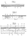
- FIG. 4 shows a card body 30 produced according to the invention.
- the electronic module 32 has been shown, of which only the external electrical contact pads 34 are visible.
- Also shown at 36 are the areas of the card body which include a graphic. The zone 36 leaves open the portion of the face of the card body 30 occupied by the external pads 34 of electrical contact.
- the electronic module 32 comprises a lead frame or a printed circuit element on which the external pads 34 are made, a semiconductor patch 40 fixed on the printed circuit or the lead frame, conductive wires 42 which connect the terminals of the patch 40 to the contact pads 34 and a coating material 44 which surrounds the patch 40 and the wires 42.
- a module 32 is glued to the support 12 at each location 38, so that each pattern has a module.
- the external face of the external contact pads is directly bonded to the support 12.
- a strip is thus obtained formed by the support 12 which comprises on one of its faces a plurality of patterns (A, B ..) each pattern further comprising an electronic module 32.
- the body of the card is produced by injection molding of a plastic material which is preferably ABS.
- Figure 3 shows the mold used. It comprises a fixed part 50 and a movable part 52. These two parts define an imprint 53 which gives the external shape of the card body.
- the fixed part 50 defines by its internal wall 54 one of the main faces of the card body.
- the movable part 52 defines by its internal wall 56 the second main face of the card body and by its internal wall 58 the edge of the card body.
- the fixed 50 and mobile 52 bearing surfaces each have a bearing surface 60 and 62, these two bearing surfaces being normally in mutual contact when the mold is closed.
- the strip formed by the support 12 is placed between the fixed part 50 and the movable part 52 of the mold.
- the strip is positioned relative to the imprint 53 so that the graphics 16 carried by the support 12, and, consequently, the electronic module 32 are perfectly positioned relative to the side wall 58 of the imprint, that is to say with respect to the edge of the card body which will be produced.
- the mold is closed.
- support 12 is pinched between staves 58 and 60 of the two parts of the mold in the zone D of the support 12 which surrounds a pattern.
- the plastic material is injected into the impression 53 by the injection nozzle 64, the ABS is preferably injected at a temperature between 220 ° C. and 280 ° C.
- the nozzle 64 is disposed in the center of the wall 56 of the movable part 52.
- the plastic material fills the imprint 53 by pressing the support 12 against the internal wall 54 of the mold.
- the plastic material surrounds the electronic module 32, with the exception of its face glued to the support 12 and it is in contact with the graphics 16.
- the decorative elements 16 are fixed on the corresponding face of the volume of plastic material by tending to separate from the support 12. This result is obtained by activating the adhesive layer 20 and the release layer 14.
- the injection nozzle opens out 64 in the face 56 of the mold, facing the electronic module. It is also possible to provide several injection nozzles. It is also possible to have injection nozzles in the lateral face 58 of the mold cavity. Preferably then the nozzles are arranged at certain "corners" of the mold imprint.
- the card body is removed from the mold in which the electronic module 32 is inserted and which includes the desired graphics 36 on its main face.
- the support 12 plays a dual role, it allows the realization of graphics, and it ensures the precise positioning of the electronic module with respect to the imprint of the mold and therefore with respect to the card body. Moreover, the outer areas of the module being glued to the support 12, they are protected against possible rising of the injection material which could tend to cover them.
- the support 12 which no longer carries either an electronic module or the graphics remains in the mold after the card has been removed.
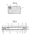
- FIG. 5 shows a variant of a mold which can be used to produce an electronic memory card having graphic elements on its two main faces.
- the mold is made up of three parts.
- a first part 70 which is mobile, comprises the part 72 of the mold cavity which defines the first main face of the card body.
- a second movable part 74 comprises the part 76 of the mold cavity which defines the second main face of the card body.
- a third part 78 fixed, which is clamped between the parts 70 and 74 of the mold when the latter is closed, comprises the part 80 of the imprint which defines the edge or the edge of the card body.
- the part 78 of the mold comprises, for example, two injection nozzles 82 and 84.
- the manufacture of a card using the mold of Figure 5 is carried out as follows: the mold is open, that is to say that the parts 70 and 74 are spaced from the fixed part 78. A film 12 supporting printing elements provided with its electronic module 32 is placed between the parts 70 and 78 of the mold as has already been described in connection with FIG. 3.
- a second film 12 ′ supporting printing elements, but without an electronic module, is placed in the same way between the parts 78 and 74 of the mold. Then we close the mold using locking means not shown in Figure 4. Thus the support films 12 and 12 'are integral with the mold since they are pinched between the three parts 70, 74 and 78 of the mold. The plastic material is then injected into the mold by the nozzles 82 and 84, and the card thus obtained is removed from the mold.
- the support film has the sole function of ensuring the positioning and the maintenance of the module in the mold. It is therefore devoid of printing elements.
- the support film must be made of a material which does not adhere to the injection material at its injection temperature c, that is to say at a temperature of the order of 200 to 280 ° C.
- the adhesive material which is used to fix the electronic module to the support film it must have certain characteristics. It must retain its adhesive properties during the filling phase of the mold. Preferably it loses, by thermal effect, its adhesive properties during the cooling phase of the molding material. Thus during the release of the card it is easily separated from the support film.
- the external contact pads are chemically cleaned to remove residual traces of adhesive material.
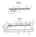
- FIG. 6 shows a support element 170.
- the support element 170 constitutes at the same time the insulating support of the electronic module.
- Element 170 consists of a sheet rectangular 174, for example ABS, which has the shape of the main faces of the card to be produced. In the suitable zone, the sheet 174 has on its external face 174 has metallizations 176 which form the external electrical contact areas of the card.
- a semiconductor patch 178 is fixed on the internal face 174b of the support 174 and connections 180 provide the electrical connection between the terminals of the semiconductor patch 178 and the external pads 176.
- the patch 178 and the connections 180 are preferably coated with insulating material 182.
- graphic prints 183 can be produced on the external face 174 a of the sheet 174 in its part not occupied by the metallizations 176.
- FIG. 7 shows in vertical section a mold 190 which can be used for the production of a card according to the second embodiment of the invention.
- the mold 190 comprises a first part 192 which defines a cavity 194 having the external shape of the body of the card to be produced.
- the part 192 of the mold comprises a plurality of vacuum systems 200 opening into the main face 192 a of the cavity 194. It also comprises an injection channel 196 opening into a "corner" of the cavity 194.
- the second part 198 of the mold 190 defines the second main face 198 a of the card body.
- the manufacture of a memory card according to this second embodiment is obtained in the following manner:
- the support element 170 which also includes the electronic module 182 is placed against the face 192 a of the part 192 of the mold.
- the vacuum systems are made active, which keeps the element 170 closed against the face 192a.
- We then close the mold by fixing the part 198 on the part 192.
- Through the injection channel 196 a suitable plastic material is penetrated which fills the cavity 194 and adheres to the internal face of the support elements 170.
- the injection material is the same as that which constitutes the support element 170.
- a memory card is thus produced which optionally includes on one of its main faces the graphic elements, graphic elements which were produced on the support element before the actual production of the card.
Abstract
Description
La présente invention concerne un procédé de réalisation de cartes à mémoire notamment électronique et des cartes obtenues par la mise en oeuvre dudit procédé.The present invention relates to a method for producing memory cards, in particular electronic cards, and to cards obtained by implementing said method.
Les cartes à mémoire comprennent essentiellement un corps de carte qui est réalisé en général en un matériau plastique et un module mémoire. Dans le cas des cartes à mémoire électronique le module mémoire est un module électronique comportant essentiellement une pastille semi-conductrice ou "chip" dans laquelle est réalisé un circuit intégré et un élément de circuit imprimé sur lequel est fixé le chip ou autre et qui définit des plages externes de contact électrique. Le module électronique est fixé dans le corps de la carte de telle manière que les plages de contact électrique affleurent une des faces principales du corps de carte.Memory cards essentially comprise a card body which is generally made of a plastic material and a memory module. In the case of electronic memory cards, the memory module is an electronic module essentially comprising a semiconductor chip or "chip" in which an integrated circuit is produced and a printed circuit element on which the chip or the like is fixed and which defines external electrical contact areas. The electronic module is fixed in the body of the card in such a way that the electrical contact pads are flush with one of the main faces of the card body.
Le corps de carte a la forme d'un parallèlèpipède rectangle dont l'épaisseur doit être inférieure à 1 mm et qui est définie par la norme ISO 7810. Les bords du corps de carte servent de référence pour le positionnement de la carte dans le lecteur de cartes de telle manière que les plages de contact de la carte viennent en contact électrique avec le connecteur du lecteur de cartes.The card body has the shape of a rectangular parallelepiped whose thickness must be less than 1 mm and which is defined by standard ISO 7810. The edges of the card body serve as a reference for positioning the card in the reader of cards in such a way that the contact areas of the card come into electrical contact with the connector of the card reader.
Il faut ajouter que le corps de carte doit en outre répondre à d'autres spécifications concernant la qualité de l'état de surface et les propriétés de tenue en flexion bien précises aussi bien selon la direction longitudinale du corps de carte que selon sa direction transversale et en torsion. Ces spécifications sont définies par la norme ISO (mentionnée ci-dessus). De plus il faut que le corps de carte ne favorise pas le stockage de charges électrostatiques.It should be added that the card body must also meet other specifications concerning the quality of the surface condition and the very precise flexural properties both in the longitudinal direction of the card body and in its transverse direction. and in torsion. These specifications are defined by the ISO standard (mentioned above). In addition, the card body must not favor the storage of electrostatic charges.
Pour résoudre ce problème on a déjà proposé dans la demande de brevet français 8700446 publiée le 22 juillet 1988 de fabriquer la carte par un procédé de moulage par injection qui comprend les étapes suivantes :
On fournit un module mémoire présentant une face d'accès et au moins un élément d'ancrage,
On place ledit module dans un moule et on le maintient en place de telle manière que la face d'accès du module mémoire soit disposée contre une paroi du moule,
On introduit dans le moule un matériau plastique de telle manière que le matériau plastique occupe la totalité de l'espace limité par les parois du moule non occupé par ledit module mémoire, et
On démoule la pièce ainsi réalisée.To resolve this problem, it has already been proposed in French patent application 8700446 published on July 22, 1988 to manufacture the card by an injection molding process which comprises the following steps:
A memory module is provided having an access face and at least one anchoring element,
The said module is placed in a mold and it is held in place in such a way that the access face of the memory module is placed against a wall of the mold,
A plastic material is introduced into the mold in such a way that the plastic material occupies the entire space limited by the walls of the mold not occupied by said memory module, and
The part thus produced is removed from the mold.
Un autre problème que pose la fabrication de cartes à mémoire est la réalisation des éléments graphiques que comporte en général au moins une des faces principales du corps de carte, ces éléments graphiques pouvant être des informations alphanumériques ou des dessins à but décoratif.Another problem posed by the manufacture of memory cards is the production of the graphic elements which generally comprises at least one of the main faces of the card body, these graphic elements possibly being alphanumeric information or drawings for decorative purposes.
Lorsque l'élément graphique présente une certaine complexité soit par la forme du tracé soit par la nature des nuances de couleur à obtenir, l'étape d'impression du graphisme, par sérigraphie ou par offset, peut conduire à un échec surtout si l'on se montre très exigeant sur la qualité du graphisme et des couleurs. En cas d'échec, il faut se résoudre à mettre au rebut les cartes dont la qualité du graphisme est jugée insuffisante. Cela signifie que les coûts en matière, en composants et en usinage des étapes de fabrication de la carte précédant l'étape de réalisation du graphisme sont perdus. Ces coûts sont particulièrement élevés si la réalisation du graphisme intervient lorsqu'un module électronique a déjà été implanté dans le corps de la carte. Cette situation se présente notamment, mais non exclusivement, lorsque la carte est fabriquée en moulant le corps de la carte directement sur le module électronique selon la technique décrite dans la demande de brevet français n° 8700446 déjà citée.When the graphic element presents a certain complexity either by the shape of the line or by the nature of the shades of color to be obtained, the stage of printing the graphics, by serigraphy or by offset, can lead to failure especially if the we are very demanding on the quality of graphics and colors. In the event of failure, it is necessary to resolve to discard the cards whose quality of graphics is considered insufficient. This means that the material, component and machining costs of the card manufacturing stages preceding the stage of graphic design are lost. These costs are particularly high if the graphics are produced when an electronic module has already been installed in the body of the card. This situation arises in particular, but not exclusively, when the card is manufactured by molding the body of the card directly on the electronic module according to the technique described in the French patent application No. 8700446 already cited.
Pour remédier à ces inconvénients un objet de l'invention est de fournir un procédé de réalisation de carte, notamment de carte à mémoire, dans lequel l'étape de réalisation du graphisme sur le corps de carte ne peut en elle-même entraîner le rejet de la carte.To overcome these drawbacks, an object of the invention is to provide a method for producing a card, in particular a memory card, in which the step of producing the graphics on the card body cannot in itself lead to rejection. from the menu.
Un objet de l'invention est de fournir un mode de réalisation d'une carte à mémoire, notamment électronique, par surmoulage du corps de carte sur le module mémoire, qui permette de plus, si on le souhaite, de réaliser les éléments graphiques dans des conditions économiques particulièrement intéressantes.An object of the invention is to provide an embodiment of a memory card, in particular electronic, by overmolding of the card body on the memory module, which also allows, if desired, to produce the graphic elements in particularly attractive economic conditions.
Pour atteindre ce but, selon l'invention le procédé de réalisation d'une carte à mémoire comprenant un corps de carte présentant deux faces principales parallèles entre elles et un module mémoire présentant une face d'accès disposée dans la première desdites faces principales du corps de carte qui se caractérise en ce qu'il comprend les étapes suivantes :To achieve this object, according to the invention the method of producing a memory card comprising a card body having two main faces parallel to each other and a memory module having an access face disposed in the first of said main faces of the body card which is characterized in that it comprises the following stages:
On fournit un moule dont l'empreinte définit la forme extérieure de ladite carte,
On fournit un élément support,
On fournit un module mémoire présentant une face d'accès, On fixe ledit module mémoire, par sa face d'accès, sur une face de l'élément support,
On place ledit élément support dans ledit moule de telle façon que sa périphérie soit solidaire dudit moule,
On injecte dans ledit moule un matériau plastique pour que celui-ci remplisse ladite empreinte du moule et que ledit module soit entouré par ledit matériau,
On démoule la pièce ainsi obtenue et on sépare l'élément support de ladite pièce, par quoi ledit module est inséré dans ledit corps, et
Après démoulage, on obtient une carte à mémoire présentant un corps de carte ayant sa forme définitive et dans lequel le module électronique est déjà implanté.A mold is provided, the imprint of which defines the external shape of said card,
We provide a support element,
We provide a memory module having an access face, We fix said memory module, by its access face, on one face of the support element,
Said support element is placed in said mold so that its periphery is integral with said mold,
Plastic material is injected into said mold so that it fills said mold cavity and said module is surrounded by said material,
The part thus obtained is removed from the mold and the support element is separated from said part, whereby said module is inserted into said body, and
After demolding, a memory card is obtained having a card body having its final shape and in which the electronic module is already installed.
Selon un mode préféré de mise en oeuvre du procédé permettant de réaliser simultanément des éléments graphiques sur la première face principale du corps de carte, l'élément support présente, sur la face sur laquelle est fixé le module mémoire, des éléments d'impression, et lors de l'injection du matériau plastique dans le moule lesdits éléments d'impression adhèrent à la face du volume de matériau injecté en contact avec l'élément support, par quoi on obtient une carte à mémoire comportant de plus des éléments graphiques sur la première face principale du corps de carte.According to a preferred embodiment of the method making it possible to simultaneously produce graphic elements on the first main face of the card body, the support element has, on the face on which the memory module is fixed, printing elements, and during the injection of the plastic material into the mold, said printing elements adhere to the face of the volume of material injected in contact with the support element, whereby a memory card is obtained comprising moreover graphic elements on the first main face of the card body.
De toutes façons l'invention sera mieux comprise à la lecture de la description qui suit de plusieurs modes de réalisation de l'invention donnés à titre d'exemples non limitatifs. La description se réfère au dessin annexé sur lequel :
- La figure 1 est une vue en coupe d'un élément support d'impression utilisable dans ladite invention,
- La figure 2 est une vue en coupe de l'élément support muni de modules électroniques,
- La figure 3 est une vue en coupe verticale d'un premier type de moule pour réaliser une carte à mémoire électronique,
- La figure 4 est une vue de dessus d'une carte à mémoire électronique, et
- La figure 5 est une vue en coupe verticale d'un deuxième type de moule pour réaliser une carte à mémoire électronique.
- La figure 6 est uen vue en coupe verticale d'un élément support muni d'un module électronique pour un deuxième mode de réalisation de l'invention et ;
- La figure 7 est une vue en coupe verticale d'un moule pour la mise en oeuvre d'un deuxième mode de réalisation de l'invention.
- FIG. 1 is a sectional view of a print support element usable in said invention,
- FIG. 2 is a sectional view of the support element provided with electronic modules,
- Figure 3 is a vertical sectional view of a first type mold to make an electronic memory card,
- FIG. 4 is a top view of an electronic memory card, and
- Figure 5 is a vertical sectional view of a second type of mold for making an electronic memory card.
- FIG. 6 is a vertical section view of a support element provided with an electronic module for a second embodiment of the invention and;
- Figure 7 is a vertical sectional view of a mold for the implementation of a second embodiment of the invention.
Avant d'expliquer plus en détails l'ensemble de l'invention on va décrire, en se référant à la figure 1, un élément support utilisable, permettant de plus de réaliser les graphismes souhaités.Before explaining in more detail the assembly of the invention, a description will be given, with reference to FIG. 1, of a support element which can be used, making it possible moreover to produce the desired graphics.
L'élément support, portant la référence 10 comporte un support 12 en matériau plastique. Le support 12 est de préférence en polyester et a une épaisseur de l'ordre de 25 micromètres.
Sur ce support 12 qui joue le rôle de support mécanique sont réalisés les éléments d'impression servant ultérieurement à obtenir le graphisme souhaité. Pour chaque élément d'impression on trouve une couche de détachement 14 ; une couche de décoration 16 constituée par des pigments ; éventuellement une couche de vernis 18 ; et une couche d'adhésif 20 dont l'épaisseur est de l'ordre de 1 à 2 micromètres.The support element, bearing the
On this
Sur une même feuille support 12 on peut réaliser un grand nombre de motifs identiques. Un tel produit est proposé notamment par la Société allemande Léonard Kurz Gmbh.A large number of identical patterns can be produced on the
En se référant maintenant aux figures 2 et 3 on va décrire un premier mode de réalisation de cartes à mémoire électronique selon l'invention.Referring now to Figures 2 and 3 we will describe a first embodiment of electronic memory cards according to the invention.
On part d'un élément support 10 qui comporte une pluralité de motifs identiques, chaque motif correspondant à l'ensemble du graphisme qui doit être réalisé sur une des faces du corps de la carte. Sur la figure 2 on a représenté les motifs A et B. Chaque motif est séparé des motifs voisins par un espace vierge dont l'utilité sera explicitée ultérieurement.We start from a
La figure 4 montre un corps de carte 30 réalisé selon l'invention. Dans la face principale visible du corps de carte on a représenté le module électronique 32 dont seules les plages externes de contact électrique 34 sont visibles. On a également représenté en 36 les zones du corps de carte qui comportent un graphisme. La zone 36 laisse dégagée la portion de la face du corps de carte 30 occupée par les plages externes 34 de contact électrique.FIG. 4 shows a
Si l'on revient à la figure 2, on voit que, pour chaque motif, la zone où des graphismes 36 sont réalisés laisse à nu la partie 38 du support plastique 12 où doit se trouver le module électronique 32, lorsque la carte est terminée.Returning to FIG. 2, it can be seen that, for each pattern, the area where
La module électronique 32 comprend un lead frame ou un élément de circuit imprimé sur lequel sont réalisées les plages externes 34, une pastille semi conductrice 40 fixée sur le circuit imprimé ou le lead frame, des fils conducteurs 42 qui relient les bornes de la pastille 40 aux plages de contact 34 et un matériau d'enrobage 44 qui entoure la pastille 40 et les fils 42. Un module 32 est collé sur le support 12 à chaque emplacement 38, de telle manière que chaque motif comporte un module.The
Comme le montre la figure 2, la face externe des plages externes de contact est directement collée sur le support 12.As shown in FIG. 2, the external face of the external contact pads is directly bonded to the
On obtient ainsi une bande formée par le support 12 qui comporte sur une de ses faces une pluralité de motifs (A, B..) chaque motif comportant de plus un module électronique 32.A strip is thus obtained formed by the
Dans l'étape suivante on réalise le corps de la carte par moulage par injection d'un matériau plastique qui est de préférence de l'ABS. La figure 3 montre le moule utilisé. Il comprend une partie fixe 50 et une partie mobile 52. Ces deux parties définissent une empreinte 53 qui donne la forme externe du corps de carte. La partie fixe 50 définit par sa paroi interne 54 une des faces principales du corps de carte. La partie mobile 52 définit par sa paroi interne 56 la deuxième face principale du corps de carte et par sa paroi interne 58 la tranche du corps de carte. Les portées fixe 50 et mobile 52 comportent chacune une portée 60 et 62, ces deux portées étant normalement en contact mutuel lorsque le moule est fermé.In the following step, the body of the card is produced by injection molding of a plastic material which is preferably ABS. Figure 3 shows the mold used. It comprises a
Le moule étant ouvert, la bande formée par le support 12 est placée entre la partie fixe 50 et la partie mobile 52 du moule. La bande est positionnée par rapport à l'empreinte 53 de telle manière que le graphisme 16 portée par le support 12, et, par voie de conséquence, le module électronique 32 soient parfaitement positionnés par rapport à la paroi latérale 58 de l'empreinte, c'est-à-dire par rapport à la tranche du corps de carte qui va être réalisé. Puis le moule est fermé. support 12 est pincé entre les portées 58 et 60 des deux parties du moule dans la zone D du support 12 qui entoure un motif. Puis on procède à l'injection du matériau plastique dans l'empreinte 53 par la buse d'injection 64, l'ABS est injecté de préférence à une température comprise entre 220°C et 280°C.. De préfèrence la buse 64 est disposée au centre de la paroi 56 de la partie mobile 52. Le matériau plastique remplit l'empreinte 53 en plaquant le support 12 contre la paroi interne 54 du moule. Le matériau plastique entoure le module électronique 32, à l'exception de sa face collée sur le support 12 et il est au contact du graphisme 16. Sous l'effet de la pression et de la température, les éléments décoratifs 16 se fixent sur la face correspondante du volume de matériau plastique en tendant à se séparer du support 12. Ce résultat est obtenu par l'activation de la couche d'adhésif 20 et de la couche de décollement 14.The mold being open, the strip formed by the
Si le module électronique 32 a une épaisseur suffisamment réduite par rapport à l'épaisseur de la carte, il est possible de prévoir que la buse d'injection débouche 64 dans la face 56 du moule, en regard du module électronique. On peut également prévoir plusieurs buses d'injection. Egalement il est possible de disposer des buses d'injection dans la face latérale 58 de l'empreinte du moule. De préfèrence alors les buses sont disposées à certains "coins" de l'empreinte du moule.If the
Après avoir ouvert le moule on démoule le corps de carte dans lequel est inserré le module électronique 32 et qui comporte le graphisme 36 désiré sur sa face principale.After opening the mold, the card body is removed from the mold in which the
On comprend que le support 12 joue un double rôle, il permet la réalisation du graphisme, et il assure le positionnement précis du module électronique par rapport à l'empreinte du moule et donc par rapport au corps de carte. De plus les plages externes du module étant collées sur le support 12, elles sont protégées contre une éventuelle remontée du matériau d'injection qui pourrait tendre à les recouvrir.It is understood that the
Le support 12 qui ne porte plus ni module électronique ni les graphismes reste dans le moule après l'enlèvement de la carte.The
La figure 5 montre une variante de moule utilisable pour réaliser une carte à mémoire électronique présentant des éléments graphiques sur ses deux faces principales. Le moule est constitué en trois parties. Une première partie 70, mobile, comporte la partie 72 de l'empreinte du moule qui définit la première face principale du corps de carte.FIG. 5 shows a variant of a mold which can be used to produce an electronic memory card having graphic elements on its two main faces. The mold is made up of three parts. A
Une deuxième partie 74, mobile, comporte la partie 76 de l'empreinte du moule qui définit la deuxième face principale du corps de carte. Une troisième partie 78, fixe, qui est enserrée entre les parties 70 et 74 du moule lorsque celui-ci est fermé, comporte la partie 80 de l'empreinte qui définit le bord ou la tranche du corps de carte. La partie 78 du moule comporte, par exemple, deux buses d'injection 82 et 84.A second
La fabrication d'une carte à l'aide du moule de la figure 5 est réalisée de la manière suivante : le moule est ouvert, c,est-à-dire que les parties 70 et 74 sont écartées de la partie fixe 78. Un film 12 support d'éléments d'impression muni de son module électronique 32 est placé entre les parties 70 et 78 du moule comme cela a déjà été décrit en liaison avec la figure 3.The manufacture of a card using the mold of Figure 5 is carried out as follows: the mold is open, that is to say that the
Un deuxième film 12′ support d'éléments d'impression, mais dépourvu de module électronique, est placé de la même manière entre les parties 78 et 74 du moule. Puis on ferme le moule à l'aide de moyens de verrouillage non représentés sur la figure 4. Ainsi les films support 12 et 12′ sont solidaires du moule puisqu'ils sont pincés entre les trois parties 70, 74 et 78 du moule. On procède ensuite à l'injection du matériau plastique dans le moule par les buses 82 et 84, et on démoule la carte ainsi obtenue.A
Dans la description précédente on a considéré le cas où un graphisme devait en outre être réalisé sur au moins une des faces principales du corps de la carte. Il va de soi que le but premier de l'invention est de fabriquer une carte à mémoire sans graphisme. Dans ce cas le film support a pour seule fonction d'assurer le positionnement et le maintien du module dans le moule. Il est donc dépourvu d'éléments d'impression. Le film support doit être réalisé en un matériau qui n'adhère pas au matériau d'injection à sa température d'injection c,est-à-dire à une température de l'ordre de 200 à 280°C. En ce qui concerne le matériau adhésif qui sert à fixer le module électronique sur le film support, il doit présenter certaines caractéristiques. Il doit conserver ses propriétés adhésives durant la phase de remplissage du moule. De préférence il perd, par effet thermique, ses propriétés adhésives lors de la phase de refroidissement du matériau de moulage. Ainsi lors du démoulage de la carte celle-ci est aisément séparée du film support. Eventuellement on procède au nettoyage chimique des plages de contact externe pour faire disparaître les traces résiduelles de matériau adhésif.In the preceding description, we have considered the case where a graphic must also be produced on at least one of the main faces of the body of the card. It goes without saying that the primary object of the invention is to manufacture a memory card without graphics. In this case, the support film has the sole function of ensuring the positioning and the maintenance of the module in the mold. It is therefore devoid of printing elements. The support film must be made of a material which does not adhere to the injection material at its injection temperature c, that is to say at a temperature of the order of 200 to 280 ° C. With regard to the adhesive material which is used to fix the electronic module to the support film, it must have certain characteristics. It must retain its adhesive properties during the filling phase of the mold. Preferably it loses, by thermal effect, its adhesive properties during the cooling phase of the molding material. Thus during the release of the card it is easily separated from the support film. Optionally, the external contact pads are chemically cleaned to remove residual traces of adhesive material.
En se référant maintenant aux figures 6 et 7 on va décrire un deuxième mode de mise en oeuvre de l'invention.Referring now to Figures 6 and 7 we will describe a second embodiment of the invention.
La figure 6 montre un élément support 170. L'élément support 170 constitue en même temps le support isolant du module électronique. L'élément 170 est constitué par une feuille rectangulaire 174, par exemple en ABS, qui a la forme des faces principales de la carte à réaliser. Dans la zone convenable, la feuille 174 comporte sur sa face externe 174a des métallisations 176 qui forment les plages externes de contact électrique de la carte. Une pastille semi-conductrice 178 est fixée sur la face interne 174b du support 174 et des connexions 180 assurent la liaison électrique entre les bornes de la pastille semi-conductrice 178 et les plages externes 176. La pastille 178 et les connexions 180 sont de préférence enrobées dans un matériau isolant 182.FIG. 6 shows a
Avant la fixation de la pastille 178, des impressions graphiques 183 peuvent être réalisées sur la face externe 174a de la feuille 174 dans sa partie non occupée par les métallisations 176.Before fixing the
La figure 7 montre en coupe verticale un moule 190 utilisable pour la réalisation d'une carte selon le deuxième mode de mise en oeuvre de l'invention. Le moule 190 comprend une première partie 192 qui définit une cavité 194 ayant la forme externe du corps de la carte à réaliser. La partie 192 du moule comprend une pluralité de systèmes à dépression 200 débouchant dans la face principale 192a de la cavité 194. Elle comprend également un canal d'injection 196 débouchant dans un "coin" de la cavité 194. La deuxième partie 198 du moule 190 définit la deuxième face principale 198a du corps de carte.FIG. 7 shows in vertical section a
La fabrication d'une carte à mémoire selon ce deuxième mode de mise en oeuvre est obtenue de la manière suivante : On met en place contre la face 192a de la partie 192 du moule l'élément support 170 qui comporte également le module électronique 182. On rend actif les systèmes à dépression ce qui maintient ferment l'élément 170 contre la face 192a. On referme alors le moule en fixant la partie 198 sur la partie 192. Par le canal d'injection 196 on fait pénétrer un matériau plastique convenable qui remplit la cavité 194 et adhère à la face interne des éléments support 170. De préfèrence le matériau d'injection est le même que celui qui constitue l' élément support 170.The manufacture of a memory card according to this second embodiment is obtained in the following manner: The
On ouvre ensuite le moule 190 et on en extrait la pièce ainsi obtenue. On réalise ainsi une carte à mémoire qui comporte éventuellement sur une de ses faces principales leséléments graphiques, éléments graphiques qui ont été réalisés sur l'élément support avant la réalisation proprement dite de la carte. Par ce procédé on obtient encore un très bon positionnement du module électronique 182 par rapport au corps de la carte. De plus il est possible d'obtenir en même temps un graphisme, l'élément support jouant de plus le rôle d'une étiquette.The
Claims (7)
On fournit un moule dont l'empreinte définit la forme extérieure de ladite carte,
On fournit un élément support,
On fournit un module mémoire présentant une face d'accès,
On fixe ledit module mémoire, par sa face d'accès, sur une face de l'élément support,
On place ledit élément support dans ledit moule de telle façon que sa périphérie soit solidaire dudit moule, On injecte dans ledit moule un matériau plastique pour que celui-ci remplisse ladite empreinte du moule et que ledit module mémoire soit entouré par le matériau plastique, et
On démoule la pièce ainsi obtenue et on sépare l'élément support de ladite pièce, par quoi ledit module mémoire est inserré dans le corps de la carte, ladite face d'accès étant disposée dans la première face principale du corps de la carte.1. A method of producing a memory card comprising a card body having two main faces parallel to each other and a memory module comprising an access face disposed in the first of said main faces of the card body, characterized in that it includes the following steps:
A mold is provided, the imprint of which defines the external shape of said card,
We provide a support element,
A memory module is provided having an access face,
Said memory module is fixed, by its access face, to one face of the support element,
Said support element is placed in said mold so that its periphery is integral with said mold, a plastic material is injected into said mold so that it fills said mold cavity and said memory module is surrounded by plastic material, and
The part thus obtained is removed from the mold and the support element is separated from said part, whereby said memory module is inserted into the body of the card, said access face being disposed in the first main face of the body of the card.
-On fournit un moule dont l'empreinte définit la forme extérieure de ladite carte ;
-On fournit un élément support en un matériau isolant ayant la forme d'une desdites faces principales ;
-On fixe une pastille semi-conductrice sur une face dudit élément support, réaliser des plages externes de contact électrique sur l'autre face dudit élément support et interconnecter électriquement lesdites plages et ladite pastille ;
-On fixe dans ledit moule ledit élément support pour que lesdites plages externes sortent appliquées contre une paroi interne dudit moule définissant une face principale de la carte ;
-On injecte dans ledit moule un matériau plastique pour que celui-ci remplisse ladite empreinte du moule et que ledit élément support adhère à la face du volume de matériau injecté en contact avec ledit élément support; et
-On démoule ladite pièce ainsi obtenue.6. Method for producing an electronic memory card comprising a body having two substantially parallel main faces, characterized in that it comprises the following steps:
-We provide a mold whose imprint defines the external shape of said card;
-We provide a support element in an insulating material having the shape of one of said main faces;
-One fixes a semiconductor patch on one side of said support element, make external electrical contact pads on the other side of said support element and electrically interconnect said pads and said pad;
-We fix in said mold said support element so that said external pads come out applied against an internal wall of said mold defining a main face of the card;
-We inject a plastic material into said mold so that it fills said mold cavity and said support member adheres to the face of the volume of material injected in contact with said support member; and
-We release said part thus obtained.
Applications Claiming Priority (4)
| Application Number | Priority Date | Filing Date | Title |
|---|---|---|---|
| FR8805671A FR2630843B1 (en) | 1988-04-28 | 1988-04-28 | PROCESS FOR PRODUCING CARDS COMPRISING GRAPHIC ELEMENTS AND CARDS OBTAINED BY SAID METHOD |
| FR8805671 | 1988-04-28 | ||
| FR8812088A FR2636755B1 (en) | 1988-09-16 | 1988-09-16 | METHOD FOR PRODUCING MEMORY CARDS AND CARDS OBTAINED BY SAID METHOD |
| FR8812088 | 1988-09-16 |
Publications (2)
| Publication Number | Publication Date |
|---|---|
| EP0340100A1 true EP0340100A1 (en) | 1989-11-02 |
| EP0340100B1 EP0340100B1 (en) | 1993-12-29 |
Family
ID=26226631
Family Applications (2)
| Application Number | Title | Priority Date | Filing Date |
|---|---|---|---|
| EP89401172A Ceased EP0340099A1 (en) | 1988-04-28 | 1989-04-25 | Manufacturing process for memory cards comprising graphic elements, and cards obtained by this process |
| EP89401173A Revoked EP0340100B1 (en) | 1988-04-28 | 1989-04-25 | Manufacturing process for memory cards, and cards obtained by this process |
Family Applications Before (1)
| Application Number | Title | Priority Date | Filing Date |
|---|---|---|---|
| EP89401172A Ceased EP0340099A1 (en) | 1988-04-28 | 1989-04-25 | Manufacturing process for memory cards comprising graphic elements, and cards obtained by this process |
Country Status (5)
| Country | Link |
|---|---|
| US (2) | US5030407A (en) |
| EP (2) | EP0340099A1 (en) |
| JP (2) | JP2812485B2 (en) |
| DE (1) | DE68911738T2 (en) |
| ES (1) | ES2049831T3 (en) |
Cited By (27)
| Publication number | Priority date | Publication date | Assignee | Title |
|---|---|---|---|---|
| EP0399868A2 (en) * | 1989-05-26 | 1990-11-28 | ESEC (Far East) Limited | Manufacturing process of a chip card and card obtained by this process |
| EP0412893A1 (en) * | 1989-08-07 | 1991-02-13 | Schlumberger Industries | Method for making card bodies and cards with graphic elements and card bodies so obtained |
| FR2661761A1 (en) * | 1990-05-07 | 1991-11-08 | Mitsubishi Electric Corp | Integrated circuit card |
| EP0488485A2 (en) * | 1990-11-27 | 1992-06-03 | MANNESMANN Aktiengesellschaft | Method and apparatus for manufacturing a decorated chip-card |
| FR2673017A1 (en) * | 1991-02-18 | 1992-08-21 | Schlumberger Ind Sa | METHOD FOR MANUFACTURING AN ELECTRONIC MODULE FOR A MEMORY CARD AND ELECTRONIC MODULE THUS OBTAINED. |
| FR2687817A1 (en) * | 1991-12-26 | 1993-08-27 | Mitsubishi Electric Corp | THIN INTEGRATED CIRCUIT CARD AND MANUFACTURING METHOD. |
| FR2704961A1 (en) * | 1993-05-04 | 1994-11-10 | Schlumberger Ind Sa | Process for manufacturing memory cards |
| US5367766A (en) * | 1990-08-01 | 1994-11-29 | Staktek Corporation | Ultra high density integrated circuit packages method |
| US5377077A (en) * | 1990-08-01 | 1994-12-27 | Staktek Corporation | Ultra high density integrated circuit packages method and apparatus |
| EP0649719A1 (en) * | 1993-10-26 | 1995-04-26 | Siemens Aktiengesellschaft | Method for manufacturing chip cards by injection moulding |
| US5420751A (en) * | 1990-08-01 | 1995-05-30 | Staktek Corporation | Ultra high density modular integrated circuit package |
| US5446620A (en) * | 1990-08-01 | 1995-08-29 | Staktek Corporation | Ultra high density integrated circuit packages |
| US5475920A (en) * | 1990-08-01 | 1995-12-19 | Burns; Carmen D. | Method of assembling ultra high density integrated circuit packages |
| GB2295118A (en) * | 1994-10-07 | 1996-05-22 | Three View Technology Co Ltd | PCMCIA Card manufacturing process |
| WO1997023843A1 (en) * | 1995-12-22 | 1997-07-03 | Sempac Sa | Process for producing a chip card for contactless operation |
| US5702985A (en) * | 1992-06-26 | 1997-12-30 | Staktek Corporation | Hermetically sealed ceramic integrated circuit heat dissipating package fabrication method |
| WO1997050056A1 (en) * | 1996-06-24 | 1997-12-31 | Siemens Aktiengesellschaft | Leadframe for the assembly of an integrated circuit in an injection mounded housing |
| WO1998042488A1 (en) * | 1997-03-21 | 1998-10-01 | Tlog | Method for including an electronic label in the wall of a heat-transformed object, preparatory device for this method, and moulded object resulting from this method |
| US6025642A (en) * | 1995-08-17 | 2000-02-15 | Staktek Corporation | Ultra high density integrated circuit packages |
| US6031242A (en) * | 1998-01-23 | 2000-02-29 | Zevatech, Inc. | Semiconductor die in-flight registration and orientation method and apparatus |
| US6077022A (en) * | 1997-02-18 | 2000-06-20 | Zevatech Trading Ag | Placement machine and a method to control a placement machine |
| US6135339A (en) * | 1998-01-26 | 2000-10-24 | Esec Sa | Ultrasonic transducer with a flange for mounting on an ultrasonic welding device, in particular on a wire bonder |
| US6157870A (en) * | 1997-02-18 | 2000-12-05 | Zevatech Trading Ag | Apparatus supplying components to a placement machine with splice sensor |
| US6185815B1 (en) | 1997-12-07 | 2001-02-13 | Esec Sa | Semiconductor mounting apparatus with a chip gripper travelling back and forth |
| CN1113314C (en) * | 1997-07-10 | 2003-07-02 | 沙诺夫公司 | Method and system for remotely recognizing electrically encoded articles |
| EP1780662A1 (en) * | 2005-10-27 | 2007-05-02 | Axalto SA | Reinforced chipcard module and method of manufacturing the same |
| US8087591B2 (en) | 2004-06-09 | 2012-01-03 | Giesecke & Devrient Gmbh | Method for producing a portable data carrier |
Families Citing this family (59)
| Publication number | Priority date | Publication date | Assignee | Title |
|---|---|---|---|---|
| US5387306A (en) * | 1988-06-21 | 1995-02-07 | Gec Avery Limited | Manufacturing integrated circuit cards |
| JPH0767874B2 (en) * | 1989-03-31 | 1995-07-26 | リズム時計工業株式会社 | IC card manufacturing method |
| US5244840A (en) * | 1989-05-23 | 1993-09-14 | Mitsubishi Denki Kabushiki Kaisha | Method for manufacturing an encapsulated IC card having a molded frame and a circuit board |
| US5417905A (en) * | 1989-05-26 | 1995-05-23 | Esec (Far East) Limited | Method of making a card having decorations on both faces |
| DE3929299A1 (en) * | 1989-08-11 | 1991-02-14 | Kurz Leonhard Fa | METHOD FOR PRODUCING CARDS |
| DE3926578C1 (en) * | 1989-08-11 | 1990-07-26 | Leonhard Kurz Gmbh & Co, 8510 Fuerth, De | |
| JP2560895B2 (en) * | 1990-07-25 | 1996-12-04 | 三菱電機株式会社 | IC card manufacturing method and IC card |
| FR2668096B1 (en) * | 1990-10-19 | 1993-01-22 | Schlumberger Ind Sa | METHOD FOR MANUFACTURING A MEMORY CARD CAPABLE OF RECEIVING A PHOTOGRAPHIC IMAGE AND CARD THUS OBTAINED. |
| WO1992020506A1 (en) * | 1991-05-10 | 1992-11-26 | GAO Gesellschaft für Automation und Organisation mbH | Process and device for manufacturing plastic mouldings having wall regions of reduced thickness |
| JP2774906B2 (en) * | 1992-09-17 | 1998-07-09 | 三菱電機株式会社 | Thin semiconductor device and method of manufacturing the same |
| FR2702067B1 (en) * | 1993-02-23 | 1995-04-14 | Schlumberger Ind Sa | Method and device for manufacturing memory cards. |
| EP0688650B1 (en) * | 1994-01-13 | 2000-11-02 | Citizen Watch Co. Ltd. | Method of resin-sealing semiconductor devices |
| US5916047A (en) * | 1994-02-03 | 1999-06-29 | Huffy Corporation | Portable basketball goal support system with separate ballast tank |
| US5980400A (en) * | 1994-02-03 | 1999-11-09 | Huffy Corporation | Compression molded basketball components with inmold graphics |
| US5626339A (en) * | 1994-02-03 | 1997-05-06 | Huffy Corporation | Structural foam basketball backboard with inmold graphics |
| JP3442877B2 (en) * | 1994-02-21 | 2003-09-02 | 富士通株式会社 | Resin molded product and manufacturing method thereof |
| DE4435802A1 (en) * | 1994-10-06 | 1996-04-11 | Giesecke & Devrient Gmbh | Method for producing data carriers with embedded elements and device for carrying out the method |
| US5846477A (en) * | 1994-12-08 | 1998-12-08 | Nitto Denko Corporation | Production method for encapsulating a semiconductor device |
| DE19504194C1 (en) * | 1995-02-09 | 1996-04-04 | Interlock Ag | ID chip card mfr. |
| US5819394A (en) * | 1995-02-22 | 1998-10-13 | Transition Automation, Inc. | Method of making board matched nested support fixture |
| JP3337847B2 (en) * | 1995-02-27 | 2002-10-28 | 株式会社東芝 | Manufacturing method of electronic component built-in card |
| DE19519899A1 (en) * | 1995-05-31 | 1996-12-12 | Richard Herbst | Method and device for producing a smart card |
| DE19519901C2 (en) * | 1995-05-31 | 1998-06-18 | Richard Herbst | Process for intermittent injection molding of plastic and semi-finished articles for use in this process |
| FR2735714B1 (en) * | 1995-06-21 | 1997-07-25 | Schlumberger Ind Sa | METHOD FOR PRINTING A GRAPHICS ON A MEMORY CARD |
| GB9520072D0 (en) * | 1995-10-02 | 1995-12-06 | Dewhurst Plc | Indicators and push-button members and method of forming the same |
| US5632408A (en) * | 1995-11-21 | 1997-05-27 | Mitchell; Jerry B. | Apparatus for securing and dispensing currency |
| DE19607212C1 (en) * | 1996-02-26 | 1997-04-10 | Richard Herbst | Prodn. of smart cards and data cards as composite injection moulding |
| US5955021A (en) * | 1997-05-19 | 1999-09-21 | Cardxx, Llc | Method of making smart cards |
| US6025054A (en) * | 1997-09-08 | 2000-02-15 | Cardxx, Inc. | Smart cards having glue-positioned electronic components |
| DE19758647A1 (en) * | 1997-11-07 | 2001-01-25 | Richard Herbst | Method and device for injection molding plastic parts |
| US6256873B1 (en) | 1998-03-17 | 2001-07-10 | Cardxx, Inc. | Method for making smart cards using isotropic thermoset adhesive materials |
| US6213341B1 (en) * | 1998-09-09 | 2001-04-10 | Brink's Incorporated | Safe for holding and dispensing change |
| GB0024070D0 (en) * | 2000-10-02 | 2000-11-15 | Innavisions Ltd | Mpulding apparatus and method |
| DE60205655D1 (en) * | 2001-11-23 | 2005-09-22 | Nagraid Sa | METHOD OF MANUFACTURING A MODULE WITH AT LEAST ONE ELECTRONIC ELEMENT |
| DE10162450B4 (en) * | 2001-12-19 | 2008-06-05 | Giesecke & Devrient Gmbh | Portable data carrier and method and device for manufacturing |
| FR2840253B1 (en) * | 2002-05-31 | 2005-03-11 | Knauf Snc | PROCESS FOR DECORATING A POLYCARBONATE SUBSTRATE OR SIMILAR MATERIAL AND DECORATED SUBSTRATE OBTAINED BY CARRYING OUT SAID METHOD |
| KR100484834B1 (en) * | 2002-11-28 | 2005-04-22 | 엘지전자 주식회사 | The display panel manufacturing mold of a washer |
| US7573048B2 (en) * | 2004-10-08 | 2009-08-11 | Patel Gordhanbhai N | Tamper resistant self indicating instant alert radiation dosimeter |
| US7237724B2 (en) * | 2005-04-06 | 2007-07-03 | Robert Singleton | Smart card and method for manufacturing a smart card |
| US7607249B2 (en) * | 2005-07-15 | 2009-10-27 | Innovatier Inc. | RFID bracelet and method for manufacturing a RFID bracelet |
| AU2007243634A1 (en) * | 2006-04-10 | 2007-11-08 | Innovatier, Inc. | An electronic inlay module for electronic cards and tags, electronic card and methods for manufacturing such electronic inlay modules and cards |
| US20070290048A1 (en) * | 2006-06-20 | 2007-12-20 | Innovatier, Inc. | Embedded electronic device and method for manufacturing an embedded electronic device |
| US20080160397A1 (en) * | 2006-08-25 | 2008-07-03 | Innovatier, Inc | Battery powered device having a protective frame |
| US20080055824A1 (en) * | 2006-08-25 | 2008-03-06 | Innovatier, Inc. | Battery powered device having a protective frame |
| JP2010522396A (en) * | 2007-03-23 | 2010-07-01 | イノベイティア インコーポレイテッド | Step card and step card manufacturing method |
| JP2011501870A (en) * | 2007-05-08 | 2011-01-13 | オッカム ポートフォリオ リミテッド ライアビリティ カンパニー | Solderless electronic assemblies and methods of manufacturing the same |
| US7926173B2 (en) | 2007-07-05 | 2011-04-19 | Occam Portfolio Llc | Method of making a circuit assembly |
| JP2010527158A (en) * | 2007-05-08 | 2010-08-05 | オッカム ポートフォリオ リミテッド ライアビリティ カンパニー | Solderless light emitting diode assembly |
| US20080282540A1 (en) * | 2007-05-14 | 2008-11-20 | Innovatier, Inc. | Method for making advanced smart cards with integrated electronics using isotropic thermoset adhesive materials with high quality exterior surfaces |
| JP4706677B2 (en) * | 2007-09-03 | 2011-06-22 | 三菱電機株式会社 | RFID tag manufacturing method |
| US20090096614A1 (en) * | 2007-10-15 | 2009-04-16 | Innovatier, Inc. | Rfid power bracelet and method for manufacturing a rfid power bracelet |
| US20090181215A1 (en) * | 2008-01-15 | 2009-07-16 | Innovatier, Inc. | Plastic card and method for making a plastic card |
| US7943434B2 (en) * | 2008-03-21 | 2011-05-17 | Occam Portfolio Llc | Monolithic molded flexible electronic assemblies without solder and methods for their manufacture |
| KR20130069564A (en) | 2010-04-05 | 2013-06-26 | 이노배티어, 인코프레이티드 | A pre-lamination core and method for making a pre-lamination core for electronic cards and tags |
| DE102012000370B4 (en) | 2012-01-11 | 2017-02-02 | Pfanner Schutzbekleidung Gmbh | Hard hat, especially for mountaineers and tree climbers |
| JP6528198B2 (en) * | 2015-04-24 | 2019-06-12 | パナソニックIpマネジメント株式会社 | Injection molding method |
| US11034068B2 (en) | 2018-04-30 | 2021-06-15 | Raytheon Company | Encapsulating electronics in high-performance thermoplastics |
| CN110696275B (en) * | 2019-10-31 | 2022-06-21 | 奇点新源国际技术开发(北京)有限公司 | Plastic package method for cable node |
| CN113276359B (en) * | 2020-02-19 | 2022-11-08 | 长鑫存储技术有限公司 | Injection mold and injection molding method |
Citations (1)
| Publication number | Priority date | Publication date | Assignee | Title |
|---|---|---|---|---|
| EP0277854B1 (en) * | 1987-01-16 | 1992-04-01 | Schlumberger Industries | Memory card manufacturing process and cards obtained by this process |
Family Cites Families (21)
| Publication number | Priority date | Publication date | Assignee | Title |
|---|---|---|---|---|
| NL255667A (en) * | 1959-09-17 | |||
| US3122598A (en) * | 1960-11-03 | 1964-02-25 | Foster Grant Co Inc | Plastic decorating method |
| US3839129A (en) * | 1970-09-25 | 1974-10-01 | Pictorial Prod Inc | Reflective foil and process |
| US3654062A (en) * | 1970-09-28 | 1972-04-04 | Standard Products Co | Injection molded decorative plaques |
| US4216577A (en) * | 1975-12-31 | 1980-08-12 | Compagnie Internationale Pour L'informatique Cii-Honeywell Bull (Societe Anonyme) | Portable standardized card adapted to provide access to a system for processing electrical signals and a method of manufacturing such a card |
| FR2442480A1 (en) * | 1978-11-21 | 1980-06-20 | Ruwa Bell Sarl | METHOD FOR PRODUCING PERSONALIZED CARDS, DEVICE FOR IMPLEMENTING THE SAME, AND CARD THUS OBTAINED |
| DE3029667A1 (en) * | 1980-08-05 | 1982-03-11 | GAO Gesellschaft für Automation und Organisation mbH, 8000 München | CARRIER ELEMENT FOR AN IC COMPONENT |
| DE3029939A1 (en) * | 1980-08-07 | 1982-03-25 | GAO Gesellschaft für Automation und Organisation mbH, 8000 München | ID CARD WITH IC COMPONENT AND METHOD FOR THEIR PRODUCTION |
| DK146709C (en) * | 1980-12-09 | 1984-05-21 | Eskesen Brdr As | PROCEDURE FOR MANUFACTURING INJECTIVE PLASTIC SUBSTANCES WITH INSERT SHEETS WITH DECORATIVE AND / OR DESCRIPTIVE PRESSURE AND APPLIANCES FOR USE IN EXERCISING THE PROCEDURE |
| DE3153769C2 (en) * | 1981-04-14 | 1995-10-26 | Gao Ges Automation Org | Plastics identity card with an internal integrated circuit |
| JPS5819740A (en) * | 1981-07-24 | 1983-02-04 | Dainippon Printing Co Ltd | Magnetic card and its production |
| DE3466108D1 (en) * | 1983-06-09 | 1987-10-15 | Flonic Sa | Method of producing memory cards, and cards obtained thereby |
| US4801561A (en) * | 1984-07-05 | 1989-01-31 | National Semiconductor Corporation | Method for making a pre-testable semiconductor die package |
| FR2579799B1 (en) * | 1985-03-28 | 1990-06-22 | Flonic Sa | METHOD FOR MANUFACTURING ELECTRONIC MEMORY CARDS AND CARDS OBTAINED ACCORDING TO SAID METHOD |
| JPS62140896A (en) * | 1985-12-13 | 1987-06-24 | 日本写真印刷株式会社 | Manufacture of integrated circuit card |
| US4779145A (en) * | 1986-02-03 | 1988-10-18 | Lemelson Jerome H | Record member for magnetic and optical recording |
| JPS62244139A (en) * | 1986-04-17 | 1987-10-24 | Citizen Watch Co Ltd | Resin sealed type pin grid array and manufacture thereof |
| FR2605144B1 (en) * | 1986-10-14 | 1989-02-24 | Flonic Sa | PROCESS FOR PRODUCING CARDS WITH ELECTRONIC MEMORY AND CARDS OBTAINED BY IMPLEMENTING SAID METHOD |
| JPS6442295A (en) * | 1987-08-10 | 1989-02-14 | Seiko Epson Corp | Memory card mounting structure |
| JPH01159295A (en) * | 1987-12-16 | 1989-06-22 | Dainippon Printing Co Ltd | Manufacture of card base material for ic card |
| US4812633A (en) * | 1988-04-08 | 1989-03-14 | Minnesota Mining And Manufacturing Company | Optical data card |
-
1989
- 1989-04-21 US US07/341,183 patent/US5030407A/en not_active Expired - Lifetime
- 1989-04-21 US US07/341,182 patent/US4961893A/en not_active Expired - Lifetime
- 1989-04-25 EP EP89401172A patent/EP0340099A1/en not_active Ceased
- 1989-04-25 ES ES89401173T patent/ES2049831T3/en not_active Expired - Lifetime
- 1989-04-25 EP EP89401173A patent/EP0340100B1/en not_active Revoked
- 1989-04-25 DE DE89401173T patent/DE68911738T2/en not_active Revoked
- 1989-04-28 JP JP1111934A patent/JP2812485B2/en not_active Expired - Fee Related
- 1989-04-28 JP JP1111933A patent/JPH0238099A/en active Pending
Patent Citations (1)
| Publication number | Priority date | Publication date | Assignee | Title |
|---|---|---|---|---|
| EP0277854B1 (en) * | 1987-01-16 | 1992-04-01 | Schlumberger Industries | Memory card manufacturing process and cards obtained by this process |
Non-Patent Citations (2)
| Title |
|---|
| PATENT ABSTRACTS OF JAPAN vol. 10, no. 45 (P-430)(2102) 21 février 1986, & JP-A-60 189586 (DAINIPPON INSATSU K.K.) 27 septembre 1985, * |
| PATENT ABSTRACTS OF JAPAN vol. 10, no. 80 (P-441)(2137) 29 mars 1986, & JP-A-60 217491 (DAINIPPON INSATSU K.K.) 31 octobre 1985, * |
Cited By (42)
| Publication number | Priority date | Publication date | Assignee | Title |
|---|---|---|---|---|
| FR2659157A2 (en) * | 1989-05-26 | 1991-09-06 | Lemaire Gerard | METHOD FOR MANUFACTURING A CARD, SAID CARD, AND CARD OBTAINED BY THIS PROCESS. |
| EP0399868A3 (en) * | 1989-05-26 | 1992-04-29 | ESEC (Far East) Limited | Manufacturing process of a chip card and card obtained by this process |
| EP0399868A2 (en) * | 1989-05-26 | 1990-11-28 | ESEC (Far East) Limited | Manufacturing process of a chip card and card obtained by this process |
| US5134773A (en) * | 1989-05-26 | 1992-08-04 | Gerard Lemaire | Method for making a credit card containing a microprocessor chip |
| EP0412893A1 (en) * | 1989-08-07 | 1991-02-13 | Schlumberger Industries | Method for making card bodies and cards with graphic elements and card bodies so obtained |
| US5173840A (en) * | 1990-05-07 | 1992-12-22 | Mitsubishi Denki Kabushiki Kaisha | Molded ic card |
| FR2661761A1 (en) * | 1990-05-07 | 1991-11-08 | Mitsubishi Electric Corp | Integrated circuit card |
| US5550711A (en) * | 1990-08-01 | 1996-08-27 | Staktek Corporation | Ultra high density integrated circuit packages |
| US6168970B1 (en) | 1990-08-01 | 2001-01-02 | Staktek Group L.P. | Ultra high density integrated circuit packages |
| US6049123A (en) * | 1990-08-01 | 2000-04-11 | Staktek Corporation | Ultra high density integrated circuit packages |
| US5367766A (en) * | 1990-08-01 | 1994-11-29 | Staktek Corporation | Ultra high density integrated circuit packages method |
| US5377077A (en) * | 1990-08-01 | 1994-12-27 | Staktek Corporation | Ultra high density integrated circuit packages method and apparatus |
| US5420751A (en) * | 1990-08-01 | 1995-05-30 | Staktek Corporation | Ultra high density modular integrated circuit package |
| US5446620A (en) * | 1990-08-01 | 1995-08-29 | Staktek Corporation | Ultra high density integrated circuit packages |
| US5475920A (en) * | 1990-08-01 | 1995-12-19 | Burns; Carmen D. | Method of assembling ultra high density integrated circuit packages |
| US5566051A (en) * | 1990-08-01 | 1996-10-15 | Staktek Corporation | Ultra high density integrated circuit packages method and apparatus |
| EP0488485A2 (en) * | 1990-11-27 | 1992-06-03 | MANNESMANN Aktiengesellschaft | Method and apparatus for manufacturing a decorated chip-card |
| EP0488485A3 (en) * | 1990-11-27 | 1992-11-19 | Mannesmann Aktiengesellschaft | Method and apparatus for manufacturing a decorated chip-card |
| FR2673017A1 (en) * | 1991-02-18 | 1992-08-21 | Schlumberger Ind Sa | METHOD FOR MANUFACTURING AN ELECTRONIC MODULE FOR A MEMORY CARD AND ELECTRONIC MODULE THUS OBTAINED. |
| EP0500168A1 (en) * | 1991-02-18 | 1992-08-26 | Schlumberger Industries | Method of manufacturing an electronic module for a chip card, and electronic module made by this method |
| US5677568A (en) * | 1991-12-26 | 1997-10-14 | Mitsubishi Denki Kabushiki Kaisha | Thin IC card |
| FR2687817A1 (en) * | 1991-12-26 | 1993-08-27 | Mitsubishi Electric Corp | THIN INTEGRATED CIRCUIT CARD AND MANUFACTURING METHOD. |
| US5702985A (en) * | 1992-06-26 | 1997-12-30 | Staktek Corporation | Hermetically sealed ceramic integrated circuit heat dissipating package fabrication method |
| FR2704961A1 (en) * | 1993-05-04 | 1994-11-10 | Schlumberger Ind Sa | Process for manufacturing memory cards |
| EP0649719A1 (en) * | 1993-10-26 | 1995-04-26 | Siemens Aktiengesellschaft | Method for manufacturing chip cards by injection moulding |
| GB2295118A (en) * | 1994-10-07 | 1996-05-22 | Three View Technology Co Ltd | PCMCIA Card manufacturing process |
| GB2295118B (en) * | 1994-10-07 | 1997-01-08 | Three View Technology Co Ltd | PCMCIA card manufacturing process |
| US6025642A (en) * | 1995-08-17 | 2000-02-15 | Staktek Corporation | Ultra high density integrated circuit packages |
| WO1997023843A1 (en) * | 1995-12-22 | 1997-07-03 | Sempac Sa | Process for producing a chip card for contactless operation |
| WO1997050056A1 (en) * | 1996-06-24 | 1997-12-31 | Siemens Aktiengesellschaft | Leadframe for the assembly of an integrated circuit in an injection mounded housing |
| US6614100B1 (en) | 1996-06-24 | 2003-09-02 | Infineon Technologies Ag | Lead frame for the installation of an integrated circuit in an injection-molded package |
| US6077022A (en) * | 1997-02-18 | 2000-06-20 | Zevatech Trading Ag | Placement machine and a method to control a placement machine |
| US6157870A (en) * | 1997-02-18 | 2000-12-05 | Zevatech Trading Ag | Apparatus supplying components to a placement machine with splice sensor |
| US6482287B1 (en) | 1997-03-21 | 2002-11-19 | Tlog | Method for including an electronic label in the wall of a heat-transformed object and preparatory device for this method |
| WO1998042488A1 (en) * | 1997-03-21 | 1998-10-01 | Tlog | Method for including an electronic label in the wall of a heat-transformed object, preparatory device for this method, and moulded object resulting from this method |
| CN1113314C (en) * | 1997-07-10 | 2003-07-02 | 沙诺夫公司 | Method and system for remotely recognizing electrically encoded articles |
| US6185815B1 (en) | 1997-12-07 | 2001-02-13 | Esec Sa | Semiconductor mounting apparatus with a chip gripper travelling back and forth |
| US6031242A (en) * | 1998-01-23 | 2000-02-29 | Zevatech, Inc. | Semiconductor die in-flight registration and orientation method and apparatus |
| US6135339A (en) * | 1998-01-26 | 2000-10-24 | Esec Sa | Ultrasonic transducer with a flange for mounting on an ultrasonic welding device, in particular on a wire bonder |
| US8087591B2 (en) | 2004-06-09 | 2012-01-03 | Giesecke & Devrient Gmbh | Method for producing a portable data carrier |
| EP1759339B1 (en) * | 2004-06-09 | 2016-05-04 | Giesecke & Devrient GmbH | Method for producing a portable data carrier |
| EP1780662A1 (en) * | 2005-10-27 | 2007-05-02 | Axalto SA | Reinforced chipcard module and method of manufacturing the same |
Also Published As
| Publication number | Publication date |
|---|---|
| DE68911738T2 (en) | 1994-05-05 |
| US4961893A (en) | 1990-10-09 |
| EP0340100B1 (en) | 1993-12-29 |
| JPH0238099A (en) | 1990-02-07 |
| ES2049831T3 (en) | 1994-05-01 |
| JP2812485B2 (en) | 1998-10-22 |
| JPH0224197A (en) | 1990-01-26 |
| EP0340099A1 (en) | 1989-11-02 |
| US5030407A (en) | 1991-07-09 |
| DE68911738D1 (en) | 1994-02-10 |
Similar Documents
| Publication | Publication Date | Title |
|---|---|---|
| EP0340100B1 (en) | Manufacturing process for memory cards, and cards obtained by this process | |
| EP0277854B1 (en) | Memory card manufacturing process and cards obtained by this process | |
| EP0412893B1 (en) | Method for making card bodies and cards with graphic elements and card bodies so obtained | |
| EP0399868B1 (en) | Manufacturing process of a chip card and card obtained by this process | |
| EP1016036B1 (en) | Method for producing a contactless electronic chip card | |
| EP0344058B1 (en) | Process for producing an electronic memory card, and electronic memory card obtained by using this process | |
| EP0500168A1 (en) | Method of manufacturing an electronic module for a chip card, and electronic module made by this method | |
| EP1076882B1 (en) | Integrated circuit card comprising an interface terminal strip and method for making same | |
| EP1451771B1 (en) | Method for making a module comprising at least an electronic component | |
| FR2738077A1 (en) | ELECTRONIC MICRO-BOX FOR ELECTRONIC MEMORY CARD AND EMBODIMENT PROCESS | |
| EP0925553B1 (en) | Method for making an assembly of electronic modules for contactless memory cards | |
| FR2636755A1 (en) | Method of producing memory cards and cards obtained by the said method | |
| EP1436773A1 (en) | Electronic module with protective bump | |
| FR2817374A1 (en) | ELECTRONIC INFORMATION SUPPORT | |
| EP1966744B1 (en) | Method for producing a microchip card | |
| WO2000072253A1 (en) | Method for producing contact chip cards with a low-cost dielectric | |
| WO2007077356A2 (en) | Method for producing a microcircuit card, and associated microcircuit card | |
| EP2341472A1 (en) | Method for manufacturing by transfer of an electronic device comprising a communication interface | |
| FR2789505A1 (en) | METHOD FOR MANUFACTURING SMART CARD PORTABLE STORAGE MEDIUM | |
| EP0915431B1 (en) | IC card and manufacturing method of such a card | |
| EP1073997A1 (en) | Method for producing a decorative item on an integrated circuit card | |
| FR2630843A1 (en) | Method of producing cards including graphics elements and cards obtained by the said method | |
| FR2797977A1 (en) | MANUFACTURING PROCESS OF A PORTABLE ELECTRONIC DEVICE INCLUDING AN OVERMOLDING STEP DIRECTLY ON THE SUPPORT FILM | |
| FR2671418A1 (en) | Process for manufacturing a memory card and memory card thus obtained | |
| FR2647571A1 (en) | Method of fabricating a card known as a chip card, and card obtained by this method |
Legal Events
| Date | Code | Title | Description |
|---|---|---|---|
| PUAI | Public reference made under article 153(3) epc to a published international application that has entered the european phase |
Free format text: ORIGINAL CODE: 0009012 |
|
| AK | Designated contracting states |
Kind code of ref document: A1 Designated state(s): BE CH DE ES FR GB IT LI NL SE |
|
| 17P | Request for examination filed |
Effective date: 19891212 |
|
| 17Q | First examination report despatched |
Effective date: 19910926 |
|
| GRAA | (expected) grant |
Free format text: ORIGINAL CODE: 0009210 |
|
| AK | Designated contracting states |
Kind code of ref document: B1 Designated state(s): BE CH DE ES FR GB IT LI NL SE |
|
| REF | Corresponds to: |
Ref document number: 68911738 Country of ref document: DE Date of ref document: 19940210 |
|
| GBT | Gb: translation of ep patent filed (gb section 77(6)(a)/1977) |
Effective date: 19940117 |
|
| ITF | It: translation for a ep patent filed |
Owner name: JACOBACCI CASETTA & PERANI S.P.A. |
|
| REG | Reference to a national code |
Ref country code: ES Ref legal event code: FG2A Ref document number: 2049831 Country of ref document: ES Kind code of ref document: T3 |
|
| PLBI | Opposition filed |
Free format text: ORIGINAL CODE: 0009260 |
|
| 26 | Opposition filed |
Opponent name: GIESECKE & DEVRIENT GMBH Effective date: 19940929 |
|
| NLR1 | Nl: opposition has been filed with the epo |
Opponent name: GIESECKE & DEVRIENT GMBH |
|
| EAL | Se: european patent in force in sweden |
Ref document number: 89401173.3 |
|
| PLBO | Opposition rejected |
Free format text: ORIGINAL CODE: EPIDOS REJO |
|
| APAC | Appeal dossier modified |
Free format text: ORIGINAL CODE: EPIDOS NOAPO |
|
| APAE | Appeal reference modified |
Free format text: ORIGINAL CODE: EPIDOS REFNO |
|
| PGFP | Annual fee paid to national office [announced via postgrant information from national office to epo] |
Ref country code: ES Payment date: 19970414 Year of fee payment: 9 |
|
| PGFP | Annual fee paid to national office [announced via postgrant information from national office to epo] |
Ref country code: CH Payment date: 19970424 Year of fee payment: 9 |
|
| PG25 | Lapsed in a contracting state [announced via postgrant information from national office to epo] |
Ref country code: ES Free format text: LAPSE BECAUSE OF NON-PAYMENT OF DUE FEES Effective date: 19980427 |
|
| PG25 | Lapsed in a contracting state [announced via postgrant information from national office to epo] |
Ref country code: LI Free format text: LAPSE BECAUSE OF NON-PAYMENT OF DUE FEES Effective date: 19980430 Ref country code: CH Free format text: LAPSE BECAUSE OF NON-PAYMENT OF DUE FEES Effective date: 19980430 |
|
| REG | Reference to a national code |
Ref country code: CH Ref legal event code: PL |
|
| PGFP | Annual fee paid to national office [announced via postgrant information from national office to epo] |
Ref country code: NL Payment date: 19990322 Year of fee payment: 11 |
|
| PGFP | Annual fee paid to national office [announced via postgrant information from national office to epo] |
Ref country code: SE Payment date: 19990413 Year of fee payment: 11 |
|
| PGFP | Annual fee paid to national office [announced via postgrant information from national office to epo] |
Ref country code: DE Payment date: 19990416 Year of fee payment: 11 |
|
| PGFP | Annual fee paid to national office [announced via postgrant information from national office to epo] |
Ref country code: GB Payment date: 19990420 Year of fee payment: 11 |
|
| PGFP | Annual fee paid to national office [announced via postgrant information from national office to epo] |
Ref country code: FR Payment date: 19990430 Year of fee payment: 11 |
|
| PGFP | Annual fee paid to national office [announced via postgrant information from national office to epo] |
Ref country code: BE Payment date: 19990517 Year of fee payment: 11 |
|
| APAC | Appeal dossier modified |
Free format text: ORIGINAL CODE: EPIDOS NOAPO |
|
| RDAH | Patent revoked |
Free format text: ORIGINAL CODE: EPIDOS REVO |
|
| RDAG | Patent revoked |
Free format text: ORIGINAL CODE: 0009271 |
|
| STAA | Information on the status of an ep patent application or granted ep patent |
Free format text: STATUS: PATENT REVOKED |
|
| 27W | Patent revoked |
Effective date: 19990616 |
|
| GBPR | Gb: patent revoked under art. 102 of the ep convention designating the uk as contracting state |
Free format text: 990616 |
|
| NLR2 | Nl: decision of opposition | ||
| APAH | Appeal reference modified |
Free format text: ORIGINAL CODE: EPIDOSCREFNO |