EP0336350A2 - Device for the optical inspection of moving surfaces - Google Patents
Device for the optical inspection of moving surfaces Download PDFInfo
- Publication number
- EP0336350A2 EP0336350A2 EP89105845A EP89105845A EP0336350A2 EP 0336350 A2 EP0336350 A2 EP 0336350A2 EP 89105845 A EP89105845 A EP 89105845A EP 89105845 A EP89105845 A EP 89105845A EP 0336350 A2 EP0336350 A2 EP 0336350A2
- Authority
- EP
- European Patent Office
- Prior art keywords
- detector
- signal
- material surface
- defect
- scanning
- Prior art date
- Legal status (The legal status is an assumption and is not a legal conclusion. Google has not performed a legal analysis and makes no representation as to the accuracy of the status listed.)
- Granted
Links
Images


Classifications
-
- G—PHYSICS
- G01—MEASURING; TESTING
- G01N—INVESTIGATING OR ANALYSING MATERIALS BY DETERMINING THEIR CHEMICAL OR PHYSICAL PROPERTIES
- G01N21/00—Investigating or analysing materials by the use of optical means, i.e. using sub-millimetre waves, infrared, visible or ultraviolet light
- G01N21/84—Systems specially adapted for particular applications
- G01N21/88—Investigating the presence of flaws or contamination
- G01N21/89—Investigating the presence of flaws or contamination in moving material, e.g. running paper or textiles
- G01N21/8901—Optical details; Scanning details
-
- G—PHYSICS
- G01—MEASURING; TESTING
- G01N—INVESTIGATING OR ANALYSING MATERIALS BY DETERMINING THEIR CHEMICAL OR PHYSICAL PROPERTIES
- G01N21/00—Investigating or analysing materials by the use of optical means, i.e. using sub-millimetre waves, infrared, visible or ultraviolet light
- G01N21/17—Systems in which incident light is modified in accordance with the properties of the material investigated
- G01N21/47—Scattering, i.e. diffuse reflection
- G01N2021/4704—Angular selective
- G01N2021/4711—Multiangle measurement
Definitions
- the invention relates to a device for the optical inspection of moving material surfaces, in which a scanning beam scans the material surface periodically along a scanning line transverse to the material movement direction and the light reflected when the material surface is scanned is received by a light receiver arrangement which is connected to a signal processing device.
- Such an automatic surface inspection system with a laser scanner is described in Melliand Textile Reports 3/1982, pages 198-202 and allows a large number of different defects in the surface of material webs to be detected.
- the light of a laser is deflected with the aid of a rotating polygon mirror across a scanning line transverse to the material movement direction of a material web.
- the polygon mirror is at the focal point of a parabolic mirror, so that the angle of incidence on the material surface is the same in the entire scanning area.
- the light reflected from the material surface is fed via a cylindrical lens into a light guide rod which acts as a concentrator and is optically coupled to a photomultiplier.
- the photomultiplier feeds evaluation electronics that evaluate changes in the intensity of the reflected light in order to discover surface information, depressions, elevations, rough spots, etc.
- the error signals recognized in an error analyzer then run at a greatly reduced data rate into a processor which controls the peripheral units Mark errors at the edge of the material and generate a log of the detected errors on the screen or printer.
- the difference in intensity in the area of defects compared to the normal surface can be so small that detection is often not possible.
- An increased sensitivity can be achieved by using two or more detectors and making a comparison with a normal pattern by means of electronic data evaluation. But even here, the extent of a defect is at best recorded without saying anything about the type of surface defect. In many cases, however, it is essential to be able to identify the type of defect in order to be able to distinguish real structural defects such as cracks or the like from less significant defects such as color deviations.
- the invention has for its object to provide a device of the type mentioned, which allows surface defects such as elevations, depressions, cracks on rapidly moving flat webs or rotating cylindrical bodies made of different materials such as textiles, paper, foils, glass and metal To identify, differentiate and spatially localize holes etc.
- the light receiver arrangement comprises two optoelectronic detector arrangements which are assigned to one another and on both sides of the moving material to be inspected arranged on the surface and with their optical axes aligned with the scanning line on the material surface.
- the reflected light of the scanning beam is observed simultaneously by two opposing optoelectronic arrangements, the common optical axis of which is congruent with the path of the scanning light point.
- a momentarily illuminated fault location results in different signals in the optoelectronic detector arrangements, the timing and intensity of which can be used to make statements about the nature and position of the fault location under consideration.
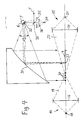
- the device for the optical inspection of moving material surfaces has as a light source a laser diode 1, to which an imaging optics 2 is assigned, which the laser diode 1 as a scanning spot 3 with a diameter of, for example, 1 micrometer or 1 millimeter onto the material surface 4 maps.
- the laser beam 5 is deflected with the aid of an oscillation mirror 6 which, for example as a resonance oscillator at 800 Hz, swings in the direction of the double arrow 7 about an axis running at right angles to the plane of the drawing.
- the scanning angle between two edge rays 8, 9 is illustrated by a double arrow 10 in the drawing.
- the scanning spot 3 describes a scanning line on the material surface 4 during the scanning movement generated by the vibration mirror 6, which is shown in FIG. 1 along the material surface 4 in extends the drawing plane between the marginal rays 8 and 9.
- the material surface 4 is, for example, a web of a textile fabric, a plastic film, a paper web, a glass web, a metal web or the surface of a rotating cylindrical body.
- an elevation 11 is exaggerated as a surface defect.
- a depression 12 is shown in dashed lines in the same place.
- the surface defect represented by the elevation 11 or the depression 12 can also be a tear, a hole or a torn fiber on a textile belt.
- a first optoelectronic detector arrangement 14 and a second optoelectronic detector arrangement 15 are assigned to the lighting device 13 described above and the material surface 4.
- the first optoelectronic detector arrangement 14 has a lens system 16, the optical axis 17 of which is aligned with the scanning line running along the material surface 4 in the plane of the drawing.
- a detector 18, which is designed as a single or multi-element detector, is arranged on the side of the lens system 16 that points away from the material surface 4. The radiation scattered from the material surface 4 into a half-cone 19 assigned to the first optoelectronic detector arrangement 14 is focused by the lens system 16 onto the detector 18.
- a pivoting adjustment telescope 39 which is shown schematically in FIG. 1 and with which the optical axis 17 coexists, is used to adjust the arrangement the material surface 4 to be examined and the light spot migrating on it can be brought to congruence.
- the second optoelectronic detector arrangement 15 shown on the right in FIG. 1 is constructed in accordance with the first detector arrangement 14 and has a lens system 20 and a detector 21. The radiation scattered over a half cone 22, of which the course of a beam in FIG. 1 is collected by the lens system 20 and imaged on the second detector 21.
- the detectors 18 and 21 are connected to a signal processing device which allows a classification of the surface defects according to type and extent.
- the detector signals feed mono-flip-flops which bring the detector signals to a suitable pulse width and control two counters running in parallel.
- the first counter is started by the signal from the first detector 18 and stopped by the signal from the second detector 21, the number of clock generator pulses counted during this time indicating the extent of the survey 11.
- the second counter comes into operation and the process is reversed.
- the second detector 21 then delivers the start pulse and the first detector 18 the stop pulse.
- FIG. 2 shows the temporal signal curve 22 of the first detector 18 and the temporal signal curve 23 of the second detector 21 for a scanning line with the elevation 11.
- the scanning spot 3 migrating to the right initially results in a falling signal curve 22, since the diffusely scattered light originates from a scanning spot 3 which is always further away.
- the scanning spot 3 comes to rest on the flank of the elevation 11 pointing to the left in FIG. 1, more scattered light reaches the detector 18, so that a pulse peak 24 occurs at the output of the detector 18.
- a depression 25 results in the signal curve 22.
- the intensity decreasing however with the distance the intensity decreasing however with the distance.
- the intensity of the scattered light initially shows continuously during a scanning movement from left to right until, due to the shadowing effect of the elevation 11, there is a signal drop 26 which is followed by a pulse peak 27 when the The scanning spot 3 is located on the flank of the elevation 11 pointing to the right in FIG. 1 towards the second detector 21.
- the pulse peaks 24 and 27 on the detectors 18, 21 occur at different times and, on the one hand, contain information about the position of the elevation 11 along the scanning line.
- the spacing of the pulse peaks 24 and 27 results in the extension of the elevation 11 in the scanning direction.
- the pulse tip 24 on the first detector 18 before the pulse tip 27 on the second Detector 21 has a possibility of classifying the surface defect as an elevation.
- the signal curve 22 shown in FIG. 3 results with a pulse peak 24 which occurs at the second detector 21 after the pulse peak 27.
- the signal processing device evaluating the signals of the detectors 18, 21 evaluates the signal profiles shown in FIGS. 2 and 3.
- a defect thus leads to different signal sequences depending on their type.
- the first detector 18 first sees the defect. After this has been exceeded, there is a brief drop, while the scanning spot 3 is in the “visual shadow” of the first detector 18.
- the procedure is reversed for the second detector 21.
- the signal at the first detector 18 rises, the signal at the second detector 21 shows a signal decrease and when the signal at the first detector 18 decreases, the signal at the second detector 21 rises.
- depressions or holes first the second detector 21 and then the detector 18 see the reflected light with the same scanning direction. The signal sequence is therefore the reverse of that for survey 11.
- the detector 18 or 21 can be designed as a single or multi-element detector, depending on the type of error to be expected.
- the geometrical relationships of the lighting device and the optoelectronic arrangements 14 and 15 result from the type and the extent of the defects to be detected, the scanning spot size, the focal length of the lens systems, their distance from the bandwidth of the material to be observed and the size of the light-sensitive areas of the Detectors 18, 21 are coordinated.
- scanning spot sizes down to the micrometer range can be realized, so that even fine cracks in metallic surfaces can be detected.
- gap-free scans can be achieved at high material speeds.
- a scanning spot size of 1 mm in diameter there is an area-wide scanning even at speeds of the order of 500 m / min.
- FIG. 4 shows an exemplary embodiment of the invention in which the material surface 4, which is shown in FIG. 4 partly as a plane and partly as threads 30 running side by side, is always acted upon by scanning light incident at right angles. This is achieved with the aid of a parabolic mirror 31, in the focal point 32 of which the pivot point of the oscillating mirror 6 is arranged. In this way, the laser beam 5, which is coupled via a beam splitter 33, is always directed perpendicularly onto the material surface 4 via the parabolic mirror 31.
- a first optoelectronic detector arrangement 14 and a second optoelectronic detector arrangement 15 are assigned to the material surface 4 in the manner described in connection with FIG. 1.
- the same components are provided with the same reference numerals as in Fig. 1.
- a third detector 34 with an aperture 35 and an image can be arranged in the arrangement according to FIG tion optics 36 may be provided.
- the third detector 34 is exposed to the directly backscattered or reflected light, whereby additional surface information is obtained. Small angle deviations of a reflecting surface 37 from the optically flat surface can also be determined if a flat multi-element detector is used as the third detector 34 instead of a single detector.
- a further embodiment relates to the arrangement of one detector line in each case normal to the observed material web instead of one individual detector.
- the detectors arranged outside the plane of the material web detect signals which, in comparison with the size of the signal detected by the detector arranged in the material plane, permit the determination of the height or depth of the defect.
- FIG. 5 shows a signal processing device 101 which can be connected to the detectors 18 and 21 and which permits the classification of surface defects.
- the signal output of the first detector 18 is connected to a first signal input 102 of the signal processing device 101.
- the first signal Input 102 is connected to a first pulse-shaping mono-flop 103 and to a first inverter 104.
- the inverted signal of the first detector 18, which is present at the output of the first inverter 104, is applied to a second mono-flop 105.
- the signal output of the second detector 18 of the inspection device according to FIG. 1 is connected to a second signal input 106 of the signal processing device 101.
- the second signal input 106 is connected to a third mono-flop 107 and to a second inverter 108.
- the inverted signal of the second detector 21, which is present at the output of the second inverter 108, is applied to a fourth mono-flop 109.
- the mono-flops 103, 105, 107 and 109 generate from the rising edges of the applied signals, which correspond to the rising and falling edges of the detector pulses 102 and 106 and which are shown in FIG. 2 in the time waveforms 22 and 23 for the two detectors 18 and 21 are shown as flanks of the pulse peaks 24 and 27, short rectangular pulses of a length of approximately 100 nanoseconds.
- the mono-flops 103, 105, 107 and 109 can be univibrators which are triggered by the positive edge of the input signal acting on them.
- the signal output 130 of the first mono-flop 103 is connected to the S input of a first flip-flop 110 and the signal output 133 of the fourth mono-flop 109 is connected to the R input of the first flip-flop 110.
- the signal output 132 of the second mono-flop 105 is connected to the S input of a second flip-flop 111 and Signal output 131 of the third mono-flop 107 is connected to the R input of the second flip-flop 111.
- the Q-transverse signal output of the first flip-flop 110 is connected via a first control line 112 to a control input of a counter and evaluation unit 113, to an input of a NAND gate 114 and to an input of an OR gate 115.
- the Q-transverse signal output of the second flip-flop 111 is connected via a second control line 116 to a further control input of the counter and evaluation unit 113, the other input of the NAND gate 114 and the other input of the OR gate 115.
- the Q output 134 of the first flip-flop 110 is connected to a first delay circuit 135, which applies the signal of the Q output 134 to it with a time delay to its output 136, the time delay being less than half the maximum occurring and detectable defect size in the material web and larger than half of the smallest occurring and detectable defect size.
- the output signal 136 of the first delay circuit 135 is logic zero if a logic zero is present at the control input 137.
- the output signal 136 of the first delay circuit 135 acts on a third inverter 137, the output of which is connected to the clock input T of the second flip-flop 111. Accordingly, the outputs of the second flip-flop 111 cannot be changed in a time period from shortly after the appearance of a first detector signal 102 to shortly after its end. The aforementioned short time period corresponds to the delay time of the first delay circuit 135.
- the Q output 138 of the second flip-flop 111 is connected to a second delay circuit 139, which applies the signal of the Q output 138 to it with a time delay at its output 140, the time delay of the time delay of the first delay circuit 135 corresponds.
- the output signal 140 of the second delay circuit 139 is logic zero if a logic zero is present at the control input 141.
- the output signal 140 of the second delay circuit 139 acts on a fourth inverter 142, the output of which is connected to the clock input T of the first flip-flop 110. Accordingly, the outputs of the first flip-flop 110 remain unchanged in a period from shortly after the appearance of a second detector signal 106 to shortly after its end. The aforementioned short period of time in turn corresponds to the delay time of the second delay circuit 139.
- both flip-flops 110 and 111 switch essentially simultaneously.
- the delay circuits 135 and 139 are switched dead via the control inputs 143 and 141 for a time which is somewhat longer than the scan time corresponding to the defect.
- the outputs of the NAND gate 114 and of the OR gate 115 are connected to further control inputs of the counter and evaluation unit 113 by a third or fourth control line 117 or 118.
- a clock signal 119 which has a frequency of 50 megahertz, is included a counter input of the counter and evaluation unit 113.
- the counter of the counter and evaluation unit 113 is started from a logic zero on the control line 117 and stopped when the signal on the control line 117 returns to logic one.
- the clock pulses of the clock generator 119 accumulated in the counting period allow the spatial extent of the error to be determined.
- a synchronization line 120 connected to the oscillating mirror drive is connected to the counter and evaluation unit 113 for this purpose.
- the position of the oscillating mirror 6 is transmitted to the counter and evaluation unit 113 via the synchronization line 120.
- the speed of the scanning beam across the material surface 4 is not constant and is dependent on the position of the oscillating mirror 6.
- the counter and evaluation unit 113 converts the error quantity for the corresponding position of the oscillating mirror 6, which is obtained from the clock signals received during the defect.
- the signal combinations that occur on the control lines 112, 116 and 118 also allow the fault to be classified as elevation 121, depression 122 or color deviation 123.
- Corresponding output signals are and are at the outputs 121, 122 and 123 of the counter and evaluation unit 113 explained in connection with FIG. 6.
- FIG. 6a schematically shows the material surface 4 of a surface web to be tested in the inspection device according to FIG. 1.
- the material surface 4 has three, drawn side by side as an example various errors 121, 122 and 123.
- the first defect is an elevation 121 in the material surface 4.
- the second defect is a depression 122 in the material surface 4.
- the third defect in the structure of the material surface 4 is a more reflective color deviation 123.
- the scanning direction between the two edge beams 8, 9 is illustrated by the directional scanning arrow 124.
- a first directional arrow 125 provided with D1 indicates the direction of observation of the first optoelectronic detector arrangement 14.
- a second directional arrow 126 provided with D2 indicates the direction of observation of the second optoelectronic detector arrangement 15.
- the directional scanning arrow 124 indicates that the movement of the scanning spot 3 from the first Optoelectronic detector arrangement 14 is directed away to the second optoelectronic detector arrangement 15.
- FIGS. 6b, 6c and 6d show temporal signal profiles in the signal processing device 101 with an elevation 121, a depression 122 or a color deviation 123, the color deviation 123 having a greater reflectivity of the material surface 4.
- the pulse-shaped input signals 102 and 106 of the signal processing device 101 are based, which result from the temporal signal curves 22 and 23 for the two Detectors 18 and 21 emerge.
- the edges that set the flip-flops 110 and 111 are illustrated with the up and down arrows.
- FIG. 6b shows waveforms for an elevation 121
- FIG. 6c shows waveforms for a depression 122
- FIG. 6d shows waveforms for a reflective color deviation 123.
- the Q and Q transverse outputs 112 and 134 of the first Flip-flops 110 and the Q and Q-transverse outputs 116 and 138 of the second flip-flop 111 are drawn, respectively.
- the further control signals 117 and 118 are generated from these signals with the aid of logic gates 114 and 115.
- an elevation 121 is characterized by a logic zero on the control line 112, the size of the defect being characterized by the number of clock pulses received by the clock generator 119 on the clock line into the counter and evaluation unit 113 .
- FIG. 6c shows that a depression 122 is characterized by a logic zero on the control line 116, the size of the defect also being characterized by the number of clock pulses arriving on the clock line 119 in the counter and evaluation unit 113.
- FIG. 6d shows signals with a color deviation 123, which is identified by a logic zero on the control line 118, the size of the defect being able to be determined analogously.
Abstract
Description
Die Erfindung betrifft eine Vorrichtung zur optischen Inspektion von bewegten Materialoberflächen, bei der ein Abtaststrahl die Materialoberfläche periodisch entlang einer Abtastlinie quer zur Materialbewegungsrichtung abtastet und das beim Überstreichen der Materialoberfläche reflektierte Licht von einer Lichtempfängeranordnung aufgenommen wird, die mit einer Signalverarbeitungseinrichtung verbunden ist.The invention relates to a device for the optical inspection of moving material surfaces, in which a scanning beam scans the material surface periodically along a scanning line transverse to the material movement direction and the light reflected when the material surface is scanned is received by a light receiver arrangement which is connected to a signal processing device.
Ein derartiges automatisches Oberflächeninspektionssystem mit Laser-Scanner ist in Melliand Textilberichte 3/1982, Seiten 198 - 202 beschrieben und gestattet es, eine Vielzahl unterschiedlicher Fehler in der Oberfläche von Warenbahnen zu erfassen. Bei der bekannten Vorrichtung wird das Licht eines Lasers mit Hilfe eines rotierenden Polygonspiegels über eine Abtastlinie quer zur Materialbewegungsrichtung einer Materialbahn abgelenkt. Bei einer telezentrischen Anordnung befindet sich der Polygonspiegel im Brennpunkt eines Parabolspiegels, so daß der Auftreffwinkel auf die Materialoberfläche im ganzen Abtastbereich gleich ist. Das von der Materialoberfläche reflektierte Licht wird über eine Zylinderlinse in einen als Konzentrator wirksamen Lichtleiterstab eingespeist, der optisch mit einem Photomultiplier gekoppelt ist. Der Photomultiplier speist eine Auswerteelektronik, die Intensitätsänderungen des zurückgeworfenen Lichtes auswertet, um Oberflächeninformationen, Vertiefungen, Erhebungen, Rauhstellen usw. zu entdecken. Die in einem Fehleranalysator erkannten Fehlersignale laufen anschließend mit stark verringerter Datenrate in einen Prozessor, der periphere Einheiten ansteuert, die Fehler am Rand des Materials markieren und über Bildschirm oder Drucker ein Protokoll der erkannten Fehler erzeugen.Such an automatic surface inspection system with a laser scanner is described in Melliand Textile
Bei einem Oberflächeninspektionssytem der oben beschriebenen Art kann der intensitätsmäßige Unterschied im Fehlerbereich zur normalen Oberfläche so gering sein, daß eine Erkennung oft nicht möglich ist. Eine erhöhte Empfindlichkeit kann dadurch erreicht werden, daß man zwei oder mehrere Detektoren verwendet und mittels elektronischer Datenauswertung einen Vergleich mit einem Normalmuster macht. Aber auch dabei wird bestenfalls die Ausdehnung einer Fehlerstelle erfaßt, ohne etwas über die Art des Oberflächendefektes auszusagen. In vielen Fällen ist es jedoch wesentlich, die Fehlerart identifizieren zu können, um echte Strukturfehler wie zum Beispiel Risse oder ähnliches von weniger bedeutenden Fehlern wie zum Beispiel Farbabweichungen unterscheiden zu können.In the case of a surface inspection system of the type described above, the difference in intensity in the area of defects compared to the normal surface can be so small that detection is often not possible. An increased sensitivity can be achieved by using two or more detectors and making a comparison with a normal pattern by means of electronic data evaluation. But even here, the extent of a defect is at best recorded without saying anything about the type of surface defect. In many cases, however, it is essential to be able to identify the type of defect in order to be able to distinguish real structural defects such as cracks or the like from less significant defects such as color deviations.
Der Erfindung liegt die Aufgabe zugrunde, eine Vorrichtung der eingangs genannten Art zu schaffen, die es gestattet, an schnell bewegten flächenhaften Bahnen oder rotierenden zylindrischen Körpern aus unterschiedlichen Materialien wie beispielsweise Textilien, Papier, Folien, Glas und Metall Oberflächendefekte wie Erhebungen, Vertiefungen, Risse, Löcher usw. festzustellen, zu unterscheiden und räumlich zu lokalisieren.The invention has for its object to provide a device of the type mentioned, which allows surface defects such as elevations, depressions, cracks on rapidly moving flat webs or rotating cylindrical bodies made of different materials such as textiles, paper, foils, glass and metal To identify, differentiate and spatially localize holes etc.
Diese Aufgabe wird erfindungsgemäß dadurch gelöst, daß die Lichtempfängeranordnung zwei einander zugeordnete optoelektronische Detektoranordnungen umfaßt, die beidseitig der zu inspizierenden bewegten Material oberfläche angeordnet und mit ihren optischen Achsen fluchtend mit der Abtastlinie auf die materialoberfläche ausgerichtet sind.This object is achieved according to the invention in that the light receiver arrangement comprises two optoelectronic detector arrangements which are assigned to one another and on both sides of the moving material to be inspected arranged on the surface and with their optical axes aligned with the scanning line on the material surface.
Durch die erfindungsgemäße Anordnung wird das reflektierte Licht des Abtaststrahles gleichzeitig von zwei einander gegenüberstehenden optoelektronischen Anordnungen beobachtet, deren gemeinsame optische Achse mit der Bahn des Abtastlichtpunktes deckungsgleich ist. Eine momentan beleuchtete Fehlerstelle ergibt in den optoelektronischen Detektoranordnungen unterschiedliche Signale, aus deren zeitlichem und intensitätsmäßigem Ablauf Aussagen über die Beschaffenheit und die Lage der betrachteten Fehlerstelle gemacht werden können. Innerhalb eines begrenzten Tiefenschärfebereiches handelt es sich um ein abbildendes System.As a result of the arrangement according to the invention, the reflected light of the scanning beam is observed simultaneously by two opposing optoelectronic arrangements, the common optical axis of which is congruent with the path of the scanning light point. A momentarily illuminated fault location results in different signals in the optoelectronic detector arrangements, the timing and intensity of which can be used to make statements about the nature and position of the fault location under consideration. Within a limited depth of field it is an imaging system.
Zweckmäßige Ausgestaltungen und Weiterbildungen der Erfindung sind in den Unteransprüchen gekennzeichnet.Expedient refinements and developments of the invention are characterized in the subclaims.
Nachfolgend werden Ausführungsbeispiele der Erfindung anhand der Zeichnung näher beschrieben. Es zeigen:
- Fig. 1 die erfindungsgemäße Vorrichtung schematisch in einem Schnitt quer zur Transportrichtung des zu überwachenden Materials,
- Fig. 2 den Signalverlauf in den beiden Detektoranordnungen bei einer Abtastung von links nach rechts in Fig. 1,
- Fig. 3 den Signalverlauf in einer der Fig. 2 ent sprechenden Darstellungsweise bei einer Abtastung von rechts nach links in Fig. 1,
- Fig. 4 eine Abwandlung der Inspektionsvorrichtung gemäß Fig. 1 mit einem immer lotrecht einfallenden Abtaststrahl und einer gegebenenfalls vorhandenen dritten Detektoranordnung für die Abtastung von teilweise spiegelnden Materialien,
- Fig. 5 eine Signalverarbeitungseinrichtung einer Inspektionsvorrichtung zum Klassifizieren von Oberflächenfehlern und
- Fig. 6 den zeitlichen Verlauf diverser Signale in der Inspektionsvorrichtung gemäß Fig. 1.
- 1 shows the device according to the invention schematically in a section transverse to the transport direction of the material to be monitored,
- 2 shows the signal curve in the two detector arrangements during a scan from left to right in FIG. 1,
- Fig. 3 ent the signal curve in one of Fig. 2 ent speaking representation in a scan from right to left in Fig. 1,
- 4 shows a modification of the inspection device according to FIG. 1 with a scanning beam which is always incident perpendicularly and an optional third detector arrangement for scanning partially reflecting materials,
- 5 shows a signal processing device of an inspection device for classifying surface defects and
- 6 shows the time course of various signals in the inspection device according to FIG. 1.
Die in Fig. 1 schematisch dargestellte Vorrichtung zur optischen Inspektion von bewegten Materialoberflächen verfügt als Lichtquelle über eine Laserdiode 1, der eine Abbildungsoptik 2 zugeordnet ist, die die Laserdiode 1 als Abtastfleck 3 mit einem Durchmesser von beispielsweise 1 Mikrometer oder 1 Millimeter auf die Materialoberfläche 4 abbildet. Der Laserstrahl 5 wird dabei mit Hilfe eines Schwingungsspiegels 6, der beispielsweise als Resonanzschwinger mit 800 Hz um eine rechtwinklig zur Zeichenebene verlaufende Achse in Richtung des Doppelpfeils 7 schwingt, umgelenkt. Der Abtastwinkel zwischen zwei Randstrahlen 8, 9 ist durch einen Doppelpfeil 10 in der Zeichnung veranschaulicht. Der Abtastfleck 3 beschreibt auf der Materialoberfläche 4 bei der durch den Schwingungsspiegel 6 erzeugten Abtastbewegung eine Abtastlinie, die sich in Fig. 1 entlang der Materialoberfläche 4 in der Zeichenebene zwischen den Randstrahlen 8 und 9 erstreckt. Bei der Materialoberfläche 4 handelt es sich beispielsweise um eine Warenbahn eines textilen Gewebes, eine Kunststoffolie, eine Papierbahn, eine Glasbahn, eine Metallbahn oder um die Oberfläche eines rotierenden zylindrischen Körpers.The device for the optical inspection of moving material surfaces, shown schematically in FIG. 1, has as a light source a laser diode 1, to which an
Auf der Materialoberfläche 4 ist übertrieben stark eine Erhebung 11 als Oberflächendefekt dargestellt. Eine Vertiefung 12 ist gestrichelt an der gleichen Stelle dargestellt. Bei dem durch die Erhebung 11 bzw. die Vertiefung 12 dargestellten Oberflächendefekt kann es sich auch um einen Riß, ein Loch oder eine ausgerissene Faser an einem Textilband handeln.On the
Der oben beschriebenen Beleuchtungseinrichtung 13 und der Materialoberfläche 4 sind eine erste optoelektronische Detektoranordnung 14 und eine zweite optoelektronische Detektoranordnung 15 zugeordnet. Die erste optoelektronische Detektoranordnung 14 weist ein Linsensystem 16 auf, dessen optische Achse 17 mit der in der Zeichenebene entlang der Materialoberfläche 4 verlaufenden Abtastlinie fluchtet. Auf der von der Materialoberfläche 4 wegweisenden Seite des Linsensystems 16 ist ein Detektor 18, der als Ein- oder Mehrelementdetektor ausgebildet ist, angeordnet. Die von der Materialoberfläche 4 in einen der ersten optoelektronischen Detektoranordnung 14 zugeordneten Halbkegel 19 gestreute Strahlung wird vom Linsensystem 16 auf den Detektor 18 fokussiert.A first
Zur Justierung der Anordnung dient ein einschwenkbares Justierfernrohr 39, das in Fig. 1 schematisch dargestellt ist und mit dem die optische Achse 17 exakt mit der zu untersuchenden Materialoberfläche 4 und dem auf ihr wandernden Lichtfleck zur Deckung gebracht werden kann. Die in Fig. 1 auf der rechten Seite gezeigte zweite optoelektronische Detektoranordnung 15 ist entsprechend der ersten Detektoranordnung 14 aufgebaut und verfügt über ein Linsensystem 20 und eine Detektor 21. Die über einen Halbkegel 22 gestreute Strahlung, von der in Fig. 1 der Verlauf eines Strahles dargestellt ist, wird vom Linsensystem 20 gesammelt und auf den zweiten Detektor 21 abgebildet.A pivoting adjustment telescope 39, which is shown schematically in FIG. 1 and with which the
Die Detektoren 18 und 21 sind mit einer Signalverarbeitungseinrichtung verbunden, die eine Klassifizierung der Oberflächendefekte nach Art und Ausdehnung gestattet. Im Falle zum Beispiel der Unterscheidung von Erhebungen 11 und Vertiefungen 12 bzw. Löchern in der Materialoberfläche 4 speisen die Detektorsignale Mono-Flip-Flops, die die Detektorsignale auf eine geeignete Impulsbreite bringen und zwei parallel laufende Zähler ansteuern. Im Falle einer Fehlstellenerhebung wird der erste Zähler durch das Signal des ersten Detektors 18 gestartet und durch das Signal des zweiten Detektors 21 gestoppt, wobei die Zahl der während dieser Zeit gezählten Taktgeneratorimpulse die Ausdehnung der Erhebung 11 anzeigt. Im Falle einer Vertiefung tritt der zweite Zähler in Funktion und der Ablauf ist umgekehrt. Der zweite Detektor 21 liefert dann den Startimpuls und der erste Detektor 18 den Stopimpuls.The
Fig. 2 zeigt den zeitlichen Signalverlauf 22 des ersten Detektors 18 und den zeitlichen Signalverlauf 23 des zweiten Detektors 21 für eine Abtastlinie mit der Erhebung 11. Bei einem in Fig. 1 von links nach rechts wandernden Abtastfleck 3 ergibt sich zunächst ein abfallender Signalverlauf 22, da das diffus gestreute Licht von einem immer weiter weg liegenden Abtastfleck 3 herrührt. Wenn der Abtastfleck 3 auf der in Fig. 1 nach links weisenden Flanke der Erhebung 11 zu liegen kommt, gelangt mehr Streulicht in den Detektor 18, so daß am Ausgang des Detektors 18 eine Impulsspitze 24 auftritt. Wenn sich der Abtastfleck 3 auf der gegenüberliegenden Flanke der Erhebung 11 befindet, ergibt sich im Signalverlauf 22 eine Vertiefung 25. Bei der weiteren Wanderung des Abtastflecks 3 gelangt schließlich wieder mehr Streulicht zum Detektor 18, wobei die Intensität jedoch mit der Entfernung weiter abnimmt.FIG. 2 shows the
Fig. 2 zeigt gestrichelt den Intensitätsverlauf am zweiten Detektor 21. Die Intensität des gestreuten Lichtes zeigt bei einer Abtastbewegung von links nach rechts zunächst stetig an, bis sich aufgrund des Abschattungseffektes der Erhebung 11 ein Signalabfall 26 ergibt, dem eine Impulsspitze 27 folgt, wenn der Abtastfleck 3 sich auf der in Fig. 1 nach rechts zum zweiten Detektor 21 weisenden Flanke der Erhebung 11 befindet.2 shows the intensity curve at the
Aus den obigen Erörterungen ergibt sich, daß die Impulsspitzen 24 und 27 an den Detektoren 18, 21 zeitlich versetzt auftreten und einerseits eine Information über die Lage der Erhebung 11 entlang der Abtastlinie enthalten. Andererseits ergibt sich aus dem Abstand der Impulsspitzen 24 und 27 die Ausdehnung der Erhebung 11 in Abtastrichtung. Schließlich ergibt sich daraus, daß die Impulsspitze 24 am ersten Detektor 18 vor der Impulsspitze 27 am zweiten Detektor 21 auftritt eine Möglichkeit zur Klassifizierung des Oberflächendefektes als Erhebung.It follows from the above discussions that the pulse peaks 24 and 27 on the
Wenn es sich bei dem Oberflächendefekt nicht um eine Erhebung 11, sondern um eine Vertiefung 12 handelt, ergibt sich der in Fig. 3 dargestellte Signalverlauf 22 mit einer Impulsspitze 24, die zeitlich nach der Impulsspitze 27 am zweiten Detektor 21 auftritt. Um zwischen einer Erhebung 11 und einer Vertiefung 12 zu unterscheiden, genügt es daher, wenn die die Signale der Detektoren 18, 21 auswertende Signalverarbeitungseinrichtung die in den Fig. 2 und 3 dargestellten Signalverläufe auswertet.If the surface defect is not an
Eine Fehlstelle führt somit je nach ihrer Art zu verschiedenen Signalabfolgen. Bei einem in Fig. 1 von links nach rechts wandernden Strahl sieht im Falle einer Erhebung 11 zuerst der erste Detektor 18 die Fehlstelle. Nach Überschreiten derselben erfolgt ein kurzzeitiger Abfall, während sich der Abtastfleck 3 im "Sichtschatten" des ersten Detektors 18 befindet. Für den zweiten Detektor 21 ist der Ablauf umgekehrt. Im Augenblick des Signalanstiegs des Signals am ersten Detektor 18 zeigt das Signal am zweiten Detektor 21 eine Signalabnahme und bei der Signalabnahme am ersten Detektor 18 steigt das Signal am zweiten Detektor 21 an. Im Falle von Vertiefungen oder Löchern sieht bei gleicher Abtastrichtung zuerst der zweite Detektor 21 und dann der Detektor 18 das reflektierte Licht. Die Signalabfolge ist also umgekehrt wir bei der Erhebung 11.A defect thus leads to different signal sequences depending on their type. In the case of a beam traveling from left to right in FIG. 1, in the case of an
Bei geeigneter Wahl von Abtastfleckgröße, Schwingspiegelfrequenz und Bewegungsgeschwindigkeit des zu untersuchenden Materials kann eine Fehlerstelle bei der Rückschwingung nochmals erfaßt werden. Die Signalabfolge ist dann genau spiegelbildlich, wodurch die Erkennungssicherheit erhöht wird. Mittels geeigneter elektronischer Auswertung können auf diese Weise auch Störsignale weitgehend eliminiert werden.With a suitable choice of scanning spot size, oscillating mirror frequency and movement speed of the Examining material, an error point in the back vibration can be detected again. The signal sequence is then exactly a mirror image, which increases the detection reliability. Using suitable electronic evaluation, interference signals can also be largely eliminated in this way.
Da die Fehlstellen näherungsweise auf die Detektoren 18, 21 abgebildet werden - wenn auch mit begrenzter Tiefenschärfe -, kann der Detektor 18 bzw. 21 je nach zu erwartender Fehlerart als Ein- oder Mehrelementdetektor ausgeführt sein.Since the defects are approximately imaged on the
Die geometrischen Verhältnisse der Beleuchtungseinrichtung und der optoelektronischen Anordnungen 14 und 15 ergeben sich aus der Art und der Ausdehnung der zu erkennenden Fehlstellen, wobei die Abtastfleckgröße, die Brennweite der Linsensysteme, deren Abstand von der zu beobachtenden Bandbreite des Materials und die Größe der lichtempfindlichen Flächen der Detektoren 18, 21 aufeinander abgestimmt sind. Bei Verwendung von Laserdioden mit fokussierender Optik lassen sind Abtastfleckgrößen bis in den Mikrometerbereich realisieren, so daß auch feine Risse in metallischen Oberflächen erfaßt werden können.The geometrical relationships of the lighting device and the
Bei Verwendung resonant schwingender Spiegel und schneller Detektoren 18, 21, zum Beispiel Lawinendioden, lassen sich lückenfreie Abtastungen bei hohen Materialgeschwindigkeiten erreichen. Bei einer Abtastfleckgröße von 1 mm Durchmesser ergibt sich eine flächendeckende Abtastung noch bei Geschwindigkeiten in der Größenordnung von 500 m/min.Using resonant oscillating mirrors and
Eine erhöhte Sicherheit der Unterscheidung von Erhebungen 11 und Vertiefungen 12 oder Löchern im untersuchten Material wird mit einem in der Zeichnung nicht gesondert dargestellten Ausführungsbeispiel erreicht, wenn die Detektoren 18, 21 jeweils aus drei passend dimensionerten, übereinander angeordneten Detektordioden gebildet sind. Der mittlere Detektor liegt dann genau auf der optischen Achse 17. Größere Erhebungen 11 oder Vertiefungen 12 werden im Verlauf der Abtastung auch in der darunter bzw. darüber liegenden Detektordiode angezeigt.An increased certainty of differentiating between
Fig. 4 zeigt ein Ausführungsbeispiel der Erfindung, bei dem die Materialoberfläche 4, die in Fig. 4 teilweise als Ebene und teilweise als nebeneinanderlaufende Fäden 30 dargestellt ist, immer mit rechtwinklig einfallendem Abtastlicht beaufschlagt wird. Dies wird mit Hilfe eines Parabolspiegels 31 erreicht, in dessen Brennpunkt 32 der Drehpunkt des Schwingspiegels 6 angeordnet ist. Auf diese Weise wird der Laserstrahl 5, der über einen Strahlteiler 33 angekoppelt wird, über den Parabolspiegel 31 immer senkrecht auf die Materialoberfläche 4 gelenkt.FIG. 4 shows an exemplary embodiment of the invention in which the
Der Materialoberfläche 4 sind in der im Zusammenhang mit Fig. 1 beschriebenen Weise eine erste optoelektronische Detektoranordnung 14 und eine zweite optoelektronische Detektoranordnung 15 zugeordnet. Gleiche Bauteile sind mit gleichen Bezugszeichen wie in Fig. 1 versehen.A first
Bei teilweise spiegelnd reflektierenden Materialien kann in der Anordnung gemäß Fig. 4 ein dritter Detektor 34 mit einer Blende 35 und einer Abbil dungsoptik 36 vorgesehen sein. Der dritte Detektor 34 wird mit dem direkt zurückgestreuten oder zurückgespiegelten Licht beaufschlagt, wodurch eine zusätzliche Oberflächeninformation gewonnen wird. Dabei können auch kleine Winkelabweichungen einer spiegelnden Fläche 37 von der optisch ebenen Fläche festgestellt werden, wenn statt eines Einzeldetektors ein flächiger Vielelementedetektor als dritter Detektor 34 verwendet wird.In the case of partially specularly reflecting materials, a
Ergänzt man die in Fig. 4 dargestellte Anordnung dahingehend, daß auf der Materialrückseite spiegelbildlich zum Parabolspiegel 31 ein zweiter Parabolspiegel angeordnet wird, in dessen Brennpunkt ein schneller Detektor angeordnet ist, dann lassen sich Löcher in der Materialoberfläche 4 eines Materials nach Größe und Lage bestimmen.If the arrangement shown in FIG. 4 is supplemented in such a way that a second parabolic mirror, in the focal point of which a rapid detector is arranged, is arranged in mirror image to the
Eine weitere, in der Zeichnung nicht dargestellte Ausgestaltung betrifft die Anordnung jeweils einer Detektorzeile normal zu der beobachteten Materialbahn anstelle jeweils eines Einzeldetektors. Mit dieser Anordnung erfassen die außerhalb der Ebene der Materialbahn angeordneten Detektoren Signale, die im Größenvergleich zu dem von dem in der Materialebene angeordneten Detektor erfaßten Signal, die Bestimmung der Höhe bzw. Tiefe der Fehlstelle gestatten.A further embodiment, not shown in the drawing, relates to the arrangement of one detector line in each case normal to the observed material web instead of one individual detector. With this arrangement, the detectors arranged outside the plane of the material web detect signals which, in comparison with the size of the signal detected by the detector arranged in the material plane, permit the determination of the height or depth of the defect.
Die Fig. 5 zeigt eine an den Detektoren 18 und 21 anschließbare Signalverarbeitungseinrichtung 101, die das Klassifizieren von Oberflächenfehlern gestattet. Der Signalausgang des ersten Detektors 18 ist mit einem ersten Signaleingang 102 der Signalverarbeitungseinrichtung 101 verbunden. Der erste Signal eingang 102 ist an ein erstes pulsformendes Mono-Flop 103 und an einen ersten Inverter 104 angeschlossen. Das invertierte Signal des ersten Detektors 18, das am Ausgang des ersten Inverters 104 anliegt, beaufschlagt ein zweites Mono-Flop 105.5 shows a
Der Signalausgang des zweiten Detektors 18 der Inspektionsvorrichtung nach Figur 1 ist mit einem zweiten Signaleingang 106 der Signalverarbeitungseinrichtung 101 verbunden. Der zweite Signaleingang 106 ist an ein drittes Mono-Flop 107 und an einen zweiten Inverter 108 angeschlossen. Das invertierte Signal des zweiten Detektors 21, das am Ausgang des zweiten Inverters 108 anliegt, beaufschlagt ein viertes Mono-Flop 109.The signal output of the
Die Mono-Flops 103, 105, 107 und 109 erzeugen aus den Anstiegsflanken der anliegenden Signale, die den Anstiegs- und Abstiegsflanken der Detektorimpulse 102 und 106 entsprechen und die in der Figur 2 in den zeitlichen Signalverläufen 22 und 23 für die beiden Detektoren 18 und 21 als Flanken der Impulsspitzen 24 und 27 dargestellt sind, kurze Rechteckimpulse einer Länge von ungefähr 100 Nanosekunden. Die Mono-Flops 103, 105, 107 und 109 können Univibratoren sein, die von der positiven Flanke des sie beaufschlagenden Eingangssignals getriggert werden.The mono-
Der Signalausgang 130 des ersten Mono-Flops 103 ist mit dem S-Eingang eines ersten Flip-Flops 110 und der Signalausgang 133 des vierten Mono-Flops 109 ist mit dem R-Eingang des ersten Flip-Flops 110 verbunden. Der Signalausgang 132 des zweiten Mono-Flops 105 ist mit dem S-Eingang eines zweiten Flip-Flops 111 und der Signalausgang 131 des dritten Mono-Flops 107 ist mit dem R-Eingang des zweiten Flip-Flops 111 verbunden.The signal output 130 of the first mono-
Der Q-quer-Signalausgang des ersten Flip-Flops 110 ist über eine erste Steuerleitung 112 an einen Steuereingang einer Zähler- und Auswerteeinheit 113, an einen Eingang eines NAND-Gliedes 114 und an einen Eingang eines ODER-Gliedes 115 angeschlossen. Der Q-quer-Signalausgang des zweiten Flip-Flops 111 ist über eine zweite Steuerleitung 116 mit einem weiteren Steuereingang der Zähler- und Auswerteeinheit 113, dem anderen Eingang des NAND-Gliedes 114 und dem anderen Eingang des ODER-Gliedes 115 verbunden.The Q-transverse signal output of the first flip-
Der Q-Ausgang 134 des ersten Flip-Flops 110 ist an eine erste Verzögerungsschaltung 135 angeschlossen, die das sie beaufschlagende Signal des Q-Ausgangs 134 mit einer zeitlichen Verzögerung an ihrem Ausgang 136 anlegt, wobei die zeitliche Verzögerung kleiner als die Hälfte der maximale auftretenden und erfaßbaren Fehlergröße in der Materialbahn und größer als die Hälfte der kleinsten auftretenden und erfaßbaren Fehlergröße ist. Das Ausgangssignal 136 der ersten Verzögerungsschaltung 135 ist Logisch-Null, wenn an dem Steuereingang 137 eine Logisch-Null anliegt. Das Ausgangssignal 136 der ersten Verzögerungsschaltung 135 beaufschlagt einen dritten Inverter 137, dessen Ausgang mit dem Takteingang T des zweiten Flip-Flops 111 verbunden ist. Dementsprechend sind die Ausgänge des zweiten Flip-Flops 111 in einer Zeitspanne von kurz nach Auftreten eines ersten Detektorsignals 102 bis kurz nach seinem Ende unveränderbar. Die genannte kurze Zeitspanne entspricht der Verzögerungszeit der ersten Verzögerungsschaltung 135.The
Der Q-Ausgang 138 des zweiten Flip-Flops 111 ist an eine zweite Verzögerungsschaltung 139 angeschlossen, die das sie beaufschlagende Signal des Q-Ausgangs 138 mit einer zeitlichen Verzögerung an ihrem Ausgang 140 anlegt, wobei die zeitliche Verzögerung der zeitlichen Verzögerung der ersten Verzögerungsschaltung 135 entspricht. Das Ausgangssignal 140 der zweiten Verzögerungsschaltung 139 ist Logisch-Null, wenn an dem Steuereingang 141 eine Logisch-Null anliegt. Das Ausgangssignal 140 der zweiten Verzögerungsschaltung 139 beaufschlagt einen vierten Inverter 142, dessen Ausgang mit dem Takteingang T des ersten Flip-Flops 110 verbunden ist. Dementsprechend bleiben die Ausgänge des ersten Flip-Flops 110 in einer Zeitspanne von kurz nach Auftreten eines zweiten Detektorsignals 106 bis kurz nach seinem Ende unverändert. Die genannte kurze Zeitspanne entspricht wiederum der Verzögerungszeit der zweiten Verzögerungsschaltung 139.The
Bei einem reflektierendem Farbfehler schalten beide Flip-Flops 110 und 111 im wesentlichen gleichzeitig um. In diesem Fall werden die Verzögerungsschaltungen 135 und 139 über die Steuereingänge 143 bzw. 141 für eine Zeit, die etwas größer als die der Fehlstelle entsprechenden Scanzeit ist, totgeschaltet.In the event of a reflective color error, both flip-
Die Ausgänge des NAND-Gliedes 114 und des ODER-Gliedes 115 sind mit einer dritten bzw. vierten Steuerleitung 117 bzw. 118 an weitere Steuereingänge der Zähler- und Auswerteeinheit 113 angeschlossen. Ein Taktsignal 119, das eine Frequenz von 50 Megahertz aufweist, ist mit einem Zähleingang der Zähler- und Auswerteeinheit 113 verbunden.The outputs of the
Der Zähler der Zähler- und Auswerteeinheit 113 wird von einer logischen Null auf der Steuerleitung 117 gestartet und bei einem Rücksprung des Signals auf der Steuerleitung 117 auf Logisch-Eins gestoppt. Die in der Zählzeitspanne aufgelaufenen Taktimpulse des Taktgenerators 119 gestatten die Bestimmung der räumlichen Ausdehnung des Fehlers. Eine mit dem Schwingspiegelantrieb verbundene Synchronisationsleitung 120 ist hierfür an die Zähler- und Auswerteeinheit 113 angeschlossen. Über die Synchronisationsleitung 120 wird die Position des Schwingspiegels 6 an die Zähler- und Auswerteeinheit 113 übermittelt. Die Geschwindigkeit des Abtaststrahles über die Materialoberfläche 4 ist nicht konstant und abhängig von der Position des Schwingspiegels 6. Die Zähler- und Auswerteeinheit 113 rechnet die sich aus den während der Fehlstelle eingelaufenen Taktsignalen ergebene Fehlergröße für die entsprechende Position des Schwingspiegels 6 um.The counter of the counter and
Die Signalkombinationen, die auf den Steuerleitungen 112, 116 und 118 auftreten, gestatten ferner die Klassifizierung des Fehlers als Erhebung 121, Vertiefung 122 oder Farbabweichung 123. Entsprechende Ausgangssignale liegen an den Ausgängen 121, 122 und 123 der Zähler- und Auswerteeinheit 113 an und sind im Zusammenhang mit der Fig. 6 erläutert.The signal combinations that occur on the
Die Fig. 6a stellt schematisch die Materialoberfläche 4 einer in der Inspektionsvorrichtung gemäß Fig. 1 zu prüfenden Oberflächenbahn dar. Die Materialoberfläche 4 weist, beispielhaft nebeneinander gezeichnet, drei verschiedene Fehler 121, 122 und 123 auf. Der erste Fehler ist eine Erhebung 121 in der Materialoberfläche 4. Bei dem zweiten Fehler handelt es sich um eine Vertiefung 122 in der Materialoberfläche 4. Der dritte, in der Struktur der Materialoberfläche 4 liegende Fehler ist eine höher reflektierende Farbabweichung 123.FIG. 6a schematically shows the
Die Abtastrichtung zwischen den zwei Randstrahlen 8, 9 ist durch den gerichteten Abtastpfeil 124 veranschaulicht.The scanning direction between the two
Ein erster, mit D1 versehener Richtungspfeil 125 kennzeichnet die Beobachtungsrichtung der ersten optoelektronischen Detektoranordnung 14. Ein zweiter, mit D2 versehener Richtungspfeil 126 kennzeichnet die Beobachtungsrichtung der zweiten optoelektronischen Detektoranordnung 15. Der gerichtete Abtastpfeil 124 zeigt an, daß die Bewegung des Abtastfleckes 3 von der ersten optoelektronischen Detektoranordnung 14 weg hin zur zweiten optoelektronischen Detektoranordnung 15 gerichtet ist.A first
Die Figuren 6b, 6c bzw. 6d zeigen zeitliche Signalverläufe in der Signalverarbeitungseinrichtung 101 bei einer Erhebung 121, einer Vertiefung 122 bzw. einer Farbabweichung 123, wobei die Farbabweichung 123 eine größere Reflektivität der Materialoberfläche 4 aufweist.FIGS. 6b, 6c and 6d show temporal signal profiles in the
In jeder der Figuren 6b, 6c und 6d liegen die impulsgeformten Eingangssignale 102 bzw. 106 der Signalverarbeitungseinrichtung 101 zugrunde, die aus den zeitlichen Signalverläufen 22 und 23 für die beiden Detektoren 18 und 21 hervorgehen. Mit den Aufwärts- bzw. Abwärtspfeilen sind die die Flip-Flops 110 und 111 setzenden Flanken verdeutlicht.In each of FIGS. 6b, 6c and 6d, the pulse-shaped input signals 102 and 106 of the
Die Fig. 6b zeigt Signalverläufe für eine Erhebung 121, die Fig. 6c zeigt Signalverläufe für eine Vertiefung 122 und die Fig. 6d zeigt Signalverläufe für eine reflektierende Farbabweichung 123. Die Q- bzw. Q-quer-Ausgänge 112 bzw. 134 des ersten Flip-Flops 110 und die Q- bzw. Q-quer-Ausgänge 116 bzw. 138 des zweiten Flip-Flops 111 sind jeweils gezeichnet. Aus diesen Signalen werden mit Hilfe der Logik-Gatter 114 und 115 die weiteren Steuersignale 117 und 118 erzeugt.FIG. 6b shows waveforms for an
Aus der Figur 6b ist zu erkennen, daß eine Erhebung 121 durch eine logische Null auf der Steuerleitung 112 gekennzeichnet ist, wobei die Größe der Fehlstelle durch die Anzahl der auf der Taktleitung von dem Taktgenerator 119 eingelaufenen Taktimpulse in die Zähler- und Auswerteeinheit 113 charakterisiert ist.It can be seen from FIG. 6b that an
Die Figur 6c zeigt, daß eine Vertiefung 122 durch eine logische Null auf der Steuerleitung 116 gekennzeichnet ist, wobei die Größe der Fehlstelle ebenfalls durch die Anzahl der auf der Taktleitung 119 eingelaufenen Taktimpulse in die Zähler- und Auswerteeinheit 113 charakterisiert ist.FIG. 6c shows that a
In der Figur 6d sind Signale bei einer Farbabweichung 123 dargestellt, die durch eine logische Null auf der Steuerleitung 118 gekennzeichnet ist, wobei die Größe der Fehlstelle analog feststellbar ist.FIG. 6d shows signals with a
Claims (14)
Applications Claiming Priority (2)
| Application Number | Priority Date | Filing Date | Title |
|---|---|---|---|
| DE3811563 | 1988-04-06 | ||
| DE3811563A DE3811563A1 (en) | 1988-04-06 | 1988-04-06 | DEVICE FOR THE OPTICAL INSPECTION OF MOVING MATERIAL SURFACES |
Publications (3)
| Publication Number | Publication Date |
|---|---|
| EP0336350A2 true EP0336350A2 (en) | 1989-10-11 |
| EP0336350A3 EP0336350A3 (en) | 1991-02-06 |
| EP0336350B1 EP0336350B1 (en) | 1994-08-17 |
Family
ID=6351491
Family Applications (1)
| Application Number | Title | Priority Date | Filing Date |
|---|---|---|---|
| EP89105845A Expired - Lifetime EP0336350B1 (en) | 1988-04-06 | 1989-04-04 | Device for the optical inspection of moving surfaces |
Country Status (3)
| Country | Link |
|---|---|
| EP (1) | EP0336350B1 (en) |
| AT (1) | ATE110169T1 (en) |
| DE (2) | DE3811563A1 (en) |
Cited By (1)
| Publication number | Priority date | Publication date | Assignee | Title |
|---|---|---|---|---|
| DE4232550A1 (en) * | 1992-09-29 | 1994-03-31 | Laser Sorter Gmbh | Measuring sizes of defects, esp. holes in materials - detecting pulsed light of varying intensity passing through or reflected by material |
Families Citing this family (1)
| Publication number | Priority date | Publication date | Assignee | Title |
|---|---|---|---|---|
| DE102017105806A1 (en) * | 2017-03-17 | 2018-09-20 | Geo. Gleistein & Sohn Gmbh | Method and device for, in particular automatic, non-destructive testing of, in particular local, state of wear of a linear or sheet-like textile structure or containing polymer fibers |
Citations (4)
| Publication number | Priority date | Publication date | Assignee | Title |
|---|---|---|---|---|
| US3695771A (en) * | 1970-08-06 | 1972-10-03 | Andras M Bardos | Method and apparatus for inspecting surfaces |
| US3781531A (en) * | 1972-06-23 | 1973-12-25 | Intec Corp | Flaw detector system utilizing a laser scanner |
| US4092068A (en) * | 1976-05-05 | 1978-05-30 | Domtar Inc. | Surface sensor |
| EP0071202A1 (en) * | 1981-07-29 | 1983-02-09 | Intec Corporation | Method and apparatus for optically inspecting a moving web of glass |
Family Cites Families (4)
| Publication number | Priority date | Publication date | Assignee | Title |
|---|---|---|---|---|
| DE2433682C3 (en) * | 1974-07-12 | 1979-02-15 | Erwin Sick Gmbh Optik-Elektronik, 7808 Waldkirch | Device for monitoring a material web or another scanning plane |
| GB1592449A (en) * | 1976-12-01 | 1981-07-08 | Ferranti Ltd | Optical inspection apparatus |
| US4323311A (en) * | 1979-05-11 | 1982-04-06 | Sira Institute Limited | Apparatus and method for detecting holes in sheet material |
| DE3223215A1 (en) * | 1982-06-22 | 1983-12-22 | Feldmühle AG, 4000 Düsseldorf | Method and device for testing transparent material webs |
-
1988
- 1988-04-06 DE DE3811563A patent/DE3811563A1/en active Granted
-
1989
- 1989-04-04 EP EP89105845A patent/EP0336350B1/en not_active Expired - Lifetime
- 1989-04-04 AT AT89105845T patent/ATE110169T1/en not_active IP Right Cessation
- 1989-04-04 DE DE58908199T patent/DE58908199D1/en not_active Expired - Fee Related
Patent Citations (4)
| Publication number | Priority date | Publication date | Assignee | Title |
|---|---|---|---|---|
| US3695771A (en) * | 1970-08-06 | 1972-10-03 | Andras M Bardos | Method and apparatus for inspecting surfaces |
| US3781531A (en) * | 1972-06-23 | 1973-12-25 | Intec Corp | Flaw detector system utilizing a laser scanner |
| US4092068A (en) * | 1976-05-05 | 1978-05-30 | Domtar Inc. | Surface sensor |
| EP0071202A1 (en) * | 1981-07-29 | 1983-02-09 | Intec Corporation | Method and apparatus for optically inspecting a moving web of glass |
Non-Patent Citations (1)
| Title |
|---|
| MELLIAND TEXTILBERICHTE, Band 3, 1982, Seiten 198-202; D. RÖSS: "Automatische Oberflächeninspektionssysteme mit Laser-Scanner" * |
Cited By (1)
| Publication number | Priority date | Publication date | Assignee | Title |
|---|---|---|---|---|
| DE4232550A1 (en) * | 1992-09-29 | 1994-03-31 | Laser Sorter Gmbh | Measuring sizes of defects, esp. holes in materials - detecting pulsed light of varying intensity passing through or reflected by material |
Also Published As
| Publication number | Publication date |
|---|---|
| ATE110169T1 (en) | 1994-09-15 |
| EP0336350B1 (en) | 1994-08-17 |
| EP0336350A3 (en) | 1991-02-06 |
| DE3811563A1 (en) | 1989-10-19 |
| DE58908199D1 (en) | 1994-09-22 |
| DE3811563C2 (en) | 1991-04-25 |
Similar Documents
| Publication | Publication Date | Title |
|---|---|---|
| DE19960653B4 (en) | Method and device for the detection or orientation of edges | |
| DE2428123C2 (en) | Arrangement for detecting defects in a material scanned by means of a laser beam | |
| DE2431107C3 (en) | Device for determining the size and concentration of suspended small particles | |
| DE3048053C2 (en) | ||
| DE2256736B2 (en) | Measuring arrangement for the automatic testing of the surface quality and evenness of a workpiece surface | |
| DE4007401C2 (en) | Device for determining a property of an object | |
| EP0304805B1 (en) | Optical scanning apparatus for a transparent web of material | |
| DE202010018630U1 (en) | Apparatus for detecting cracks in semiconductor substrates | |
| EP0052813A2 (en) | Method for the examination of a moving reflecting or transparent sheet, and device for carrying out said method | |
| DE3446355A1 (en) | OPTICAL TROUBLESHOOTING DEVICE | |
| DE2620240A1 (en) | METHOD AND DEVICE FOR TESTING LIGHTNUT TRANSLUCENT WORKPIECES | |
| DE4304678C1 (en) | Method for continuously scanning and checking track applications on a moving surface and device for carrying out the method | |
| EP0716287B1 (en) | Device for measuring a position of webs or sheets | |
| EP0230892A2 (en) | Optical detection means with a mirror wheel | |
| DE3534018C2 (en) | ||
| DE19914962C2 (en) | Optoelectronic device | |
| WO1989001147A1 (en) | Process for quality control of a flat object, in particular for detecting defects in textile fabrics, and device for this purpose | |
| EP0336350B1 (en) | Device for the optical inspection of moving surfaces | |
| EP0169444A2 (en) | Roughness probe | |
| DE3020044C2 (en) | ||
| DE3232885A1 (en) | METHOD FOR AUTOMATICALLY INSPECTING SURFACES | |
| DE2154086C3 (en) | Device for photoelectrically scanning a continuously moving sheet of flat glass for automatic error detection | |
| EP0052812A2 (en) | Method for the detection of defect signals using an integrating differential amplifier | |
| DE2251915A1 (en) | DEVICE FOR DETECTING SPARKS OR DEFECTS IN A SURFACE | |
| DE2655704B2 (en) | Device for detecting foreign bodies in glass bottles |
Legal Events
| Date | Code | Title | Description |
|---|---|---|---|
| PUAI | Public reference made under article 153(3) epc to a published international application that has entered the european phase |
Free format text: ORIGINAL CODE: 0009012 |
|
| AK | Designated contracting states |
Kind code of ref document: A2 Designated state(s): AT BE CH DE ES FR GB GR IT LI LU NL SE |
|
| PUAL | Search report despatched |
Free format text: ORIGINAL CODE: 0009013 |
|
| 17P | Request for examination filed |
Effective date: 19901214 |
|
| AK | Designated contracting states |
Kind code of ref document: A3 Designated state(s): AT BE CH DE ES FR GB GR IT LI LU NL SE |
|
| 17Q | First examination report despatched |
Effective date: 19921202 |
|
| GRAA | (expected) grant |
Free format text: ORIGINAL CODE: 0009210 |
|
| AK | Designated contracting states |
Kind code of ref document: B1 Designated state(s): AT BE CH DE ES FR GB GR IT LI LU NL SE |
|
| PG25 | Lapsed in a contracting state [announced via postgrant information from national office to epo] |
Ref country code: IT Free format text: LAPSE BECAUSE OF FAILURE TO SUBMIT A TRANSLATION OF THE DESCRIPTION OR TO PAY THE FEE WITHIN THE PRE;WARNING: LAPSES OF ITALIAN PATENTS WITH EFFECTIVE DATE BEFORE 2007 MAY HAVE OCCURRED AT ANY TIME BEFORE 2007. THE CORRECT EFFECTIVE DATE MAY BE DIFFERENT FROM THE ONE RECORDED.SCRIBED TIME-LIMIT Effective date: 19940817 Ref country code: GR Free format text: LAPSE BECAUSE OF FAILURE TO SUBMIT A TRANSLATION OF THE DESCRIPTION OR TO PAY THE FEE WITHIN THE PRESCRIBED TIME-LIMIT Effective date: 19940817 Ref country code: ES Free format text: THE PATENT HAS BEEN ANNULLED BY A DECISION OF A NATIONAL AUTHORITY Effective date: 19940817 Ref country code: BE Effective date: 19940817 Ref country code: NL Effective date: 19940817 |
|
| REF | Corresponds to: |
Ref document number: 110169 Country of ref document: AT Date of ref document: 19940915 Kind code of ref document: T |
|
| GBT | Gb: translation of ep patent filed (gb section 77(6)(a)/1977) |
Effective date: 19940815 |
|
| REF | Corresponds to: |
Ref document number: 58908199 Country of ref document: DE Date of ref document: 19940922 |
|
| PG25 | Lapsed in a contracting state [announced via postgrant information from national office to epo] |
Ref country code: SE Effective date: 19941117 |
|
| ET | Fr: translation filed | ||
| NLV1 | Nl: lapsed or annulled due to failure to fulfill the requirements of art. 29p and 29m of the patents act | ||
| PGFP | Annual fee paid to national office [announced via postgrant information from national office to epo] |
Ref country code: GB Payment date: 19950317 Year of fee payment: 7 |
|
| PGFP | Annual fee paid to national office [announced via postgrant information from national office to epo] |
Ref country code: FR Payment date: 19950329 Year of fee payment: 7 |
|
| PG25 | Lapsed in a contracting state [announced via postgrant information from national office to epo] |
Ref country code: AT Effective date: 19950404 |
|
| PGFP | Annual fee paid to national office [announced via postgrant information from national office to epo] |
Ref country code: DE Payment date: 19950422 Year of fee payment: 7 |
|
| PG25 | Lapsed in a contracting state [announced via postgrant information from national office to epo] |
Ref country code: LU Free format text: LAPSE BECAUSE OF NON-PAYMENT OF DUE FEES Effective date: 19950430 Ref country code: LI Effective date: 19950430 Ref country code: CH Effective date: 19950430 |
|
| PLBE | No opposition filed within time limit |
Free format text: ORIGINAL CODE: 0009261 |
|
| STAA | Information on the status of an ep patent application or granted ep patent |
Free format text: STATUS: NO OPPOSITION FILED WITHIN TIME LIMIT |
|
| 26N | No opposition filed | ||
| REG | Reference to a national code |
Ref country code: CH Ref legal event code: PL |
|
| PG25 | Lapsed in a contracting state [announced via postgrant information from national office to epo] |
Ref country code: GB Effective date: 19960404 |
|
| GBPC | Gb: european patent ceased through non-payment of renewal fee |
Effective date: 19960404 |
|
| PG25 | Lapsed in a contracting state [announced via postgrant information from national office to epo] |
Ref country code: FR Effective date: 19961227 |
|
| PG25 | Lapsed in a contracting state [announced via postgrant information from national office to epo] |
Ref country code: DE Effective date: 19970101 |
|
| REG | Reference to a national code |
Ref country code: FR Ref legal event code: ST |