EP0333407A2 - Resist material and process for information of resist patterns - Google Patents
Resist material and process for information of resist patterns Download PDFInfo
- Publication number
- EP0333407A2 EP0333407A2 EP89302448A EP89302448A EP0333407A2 EP 0333407 A2 EP0333407 A2 EP 0333407A2 EP 89302448 A EP89302448 A EP 89302448A EP 89302448 A EP89302448 A EP 89302448A EP 0333407 A2 EP0333407 A2 EP 0333407A2
- Authority
- EP
- European Patent Office
- Prior art keywords
- resist
- polymeric material
- water
- photo
- acid
- Prior art date
- Legal status (The legal status is an assumption and is not a legal conclusion. Google has not performed a legal analysis and makes no representation as to the accuracy of the status listed.)
- Ceased
Links
Images
Classifications
-
- G—PHYSICS
- G03—PHOTOGRAPHY; CINEMATOGRAPHY; ANALOGOUS TECHNIQUES USING WAVES OTHER THAN OPTICAL WAVES; ELECTROGRAPHY; HOLOGRAPHY
- G03F—PHOTOMECHANICAL PRODUCTION OF TEXTURED OR PATTERNED SURFACES, e.g. FOR PRINTING, FOR PROCESSING OF SEMICONDUCTOR DEVICES; MATERIALS THEREFOR; ORIGINALS THEREFOR; APPARATUS SPECIALLY ADAPTED THEREFOR
- G03F7/00—Photomechanical, e.g. photolithographic, production of textured or patterned surfaces, e.g. printing surfaces; Materials therefor, e.g. comprising photoresists; Apparatus specially adapted therefor
- G03F7/004—Photosensitive materials
- G03F7/0045—Photosensitive materials with organic non-macromolecular light-sensitive compounds not otherwise provided for, e.g. dissolution inhibitors
-
- G—PHYSICS
- G03—PHOTOGRAPHY; CINEMATOGRAPHY; ANALOGOUS TECHNIQUES USING WAVES OTHER THAN OPTICAL WAVES; ELECTROGRAPHY; HOLOGRAPHY
- G03F—PHOTOMECHANICAL PRODUCTION OF TEXTURED OR PATTERNED SURFACES, e.g. FOR PRINTING, FOR PROCESSING OF SEMICONDUCTOR DEVICES; MATERIALS THEREFOR; ORIGINALS THEREFOR; APPARATUS SPECIALLY ADAPTED THEREFOR
- G03F7/00—Photomechanical, e.g. photolithographic, production of textured or patterned surfaces, e.g. printing surfaces; Materials therefor, e.g. comprising photoresists; Apparatus specially adapted therefor
- G03F7/004—Photosensitive materials
- G03F7/038—Macromolecular compounds which are rendered insoluble or differentially wettable
Definitions
- the present invention relates to a resist technology, and more particularly, to a pattern-forming resist material suitable for forming negative resist patterns using deep ultraviolet (UV) radiation as an exposure radiation.
- the resist patterns are usually formed on a substrate or base material, i.e., a semiconductor material, during the production of semiconductor devices such as large-scale integrated (LSI) circuits, very-large-scale integrated (VLSI) circuits, and bubble memory devices.
- LSI large-scale integrated
- VLSI very-large-scale integrated
- bubble memory devices i.e., a semiconductor material
- a plurality of pattern-forming resist materials such as rubber-like resists, photocomposable polymeric resists and novolac resin resists, as well as different exposure radiations such as ultraviolet (UV) rays, electron beams, X-rays, and ion beams, are widely used.
- UV radiation has replaced the usual UV radiation, as the deep UV radiation has a wavelength of about 200 to 300 nm, which is shorter than that of the usual UV radiation, and can satisfy the requirements for a greater a degree of fine fabrication in the resulting resist patterns.
- cross-linking resists wherein a cross-linkable polymer such as polyvinyl alcohol is combined with a cross-linking agent such as diazonium salts, but these resists have an unsatisfactory pattern resolution due to swelling of the resulting resist patterns.
- the reason for the swelling of the resist patterns is as follows:
- n denotes a polymerization degree
- a diazonium salt of the formula: as a cross-linking agent is used as a resist material, and the resist material is selectively exposed to deep UV radiation
- PVA in the exposed areas becomes insoluble in water as a result of the cross-linking thereof.
- the water-insoluble resist pattern thus formed is represented by the following formula: in which n is as defined above.
- This cross-linking reaction occurs at a small portion of hydroxyl groups in PVA, because the concentration of the cross-linker is low. And thus, since the most of hydroxyl groups in PVA remains unchanged, the polymer remains hydrophilic even after the cross-linking reaction. Therefore, during development, water diffuses into the polymer and results in swelling.
- An object of the present invention is to provide a novel pattern-forming resist material particularly suitable for deep UV exposure and formation of fine negative resist patterns having a high sensitivity, a resistance to dry etching, and a good resolution.
- Another object of the present invention is to provide a novel process for the formation of resist patterns, in which the problem of swelling of the patterns due to absorption of water used during development is eliminated.
- a pattern-forming resist material comprising a mixture of a water-soluble polymeric material having at least one hydroxyl group in the molecular structure thereof and a photo-acid generator which, during exposure to radiation, does not cause cross-linking of said polymeric material, but releases an acid upon reaction with said polymeric material, the product of reacting the thus reacted polymeric material with said acid on heating in the presence of said acid as catalyst providing a water-insoluble polymeric material as a result of removal of water from said reacted polymeric material, which dewatered polymeric material, when present as a substrate, if said exposure has been to patterning radiation, then provides resist patterns when developed with water.
- a process for the formation of a resist pattern comprising coating a solution of a resist material according to the invention onto a substrate to form a resist layer, exposing said resist layer to patterning radiation to cause reaction of said polymeric material and said photo-acid generator and release of said acid, heating the exposed resist layer in the presence of said acid as a catalyst to remove water from the thus reacted polymeric material in said resist layer, thereby insolubilizing said reaction product in water, and developing said resist layer with water to remove said water-soluble polymeric material in unexposed areas of said layer to form resist patterns on said substrate.
- the resist patterns are formed as follows, for example:
- a semiconductor substrate 1 for example, a silicon substrate or wafer, is prepared and washed to obtain clean surfaces.
- the substrate 1 may carry any circuit parts or other elements, if desired; for example, an insulating layer such as SiO2 layer, circuits such as Al circuits, and the like.
- a resist material to be coated on the cleaned surface of the substrate 1 is prepared by mixing a water-soluble, hydroxyl group-containing polymeric material with a photo-acid generator, i.e., a compound capable of photographically producing and releasing an acid as a result of radiation exposure of the resist material.
- a photo-acid generator i.e., a compound capable of photographically producing and releasing an acid as a result of radiation exposure of the resist material.
- PVA of the formula: wherein n denotes a polymerization degree is used as the polymeric material
- a diazonium salt of the formula: wherein X1 represents a halogen atom such as C1 is used as the photo-acid generator.
- the resist material is coated on the substrate 1 to form a resist layer 2. Since this polymeric material has a good solubility in water, coating is generally carried out by conventional coating methods such as spin coating using an aqueous solution of the resist material, and the coated resist material is then dried.
- the resulting resist layer 2 is then selectively exposed to patterning radiation (deep UV used herein) h ⁇ through a mask (not shown), as illustrated in Fig. 1C.
- the wavelength of the deep UV may be a commonly used one, i.e., 240 to 250 nm.
- the following reaction proceeds in the exposed area of the resist layer 2: wherein 1 and m are intergers whose total combined with the number of phenoxy groups present is equal to n.
- the exposed resist layer is then heated to a temperature of, for example, about 100°C, and during this heating, the following reaction proceeds in the exposed area of the resist layer 2. Namely, an elimination reaction of the hydroxyl group occurs in the presence of the acid HX1 as a catalyst generated in the exposure step. Since water has been removed from the reaction product, the product 22 in the exposed area of the resist layer 2 now shows an insolubility in water (see, Fig. 1D). Namely, the exposed area is insolubilized in water, but the unexposed area remains water-soluble.
- the resist layer is developed with water to wash the unexposed area therefrom, and as shown in Fig. 1E, water-insoluble negative resist patterns 22 are thus formed on the substrate 1.
- the resulting resist patterns do not suffer from swelling thereof, with the result that these resist patterns are very fine or have an increased resolution.
- the precursor thereof i.e., the photo-acid generator
- the photo-acid generator gives satisfactory effects, even if used in a small amount of 10% by weight or less.
- a resist material having a small amount of the photo-acid generator incorporated therein has a good transparency to deep UV. The loss of resolution caused by excessively high light absorption such as in the prior art novolac resists is eliminated.
- the pattern-forming resist material according to the present invention comprises a water-soluble polymeric material, as a basic polymer, and a photo-acid generator.
- the polymeric material does not have an aromatic ring such as benzene ring in the molecular structure thereof, as an aromatic ring-free polymeric material ensures the formation of fine resist patterns, because it does not suffer from the reduced resolution caused by specific absorption characteristics of the aromatic ring.
- the polymeric material has a structure in which a carbon atom adjacent to another carbon atom to which the hydroxyl group is bonded in the polymeric material contains at least one hydrogen atom which can be combined with the split-off hydroxyl group during the heating step to form water, which is then removed from the polymeric material.
- the polymeric material used in the present invention may have a wide range of molecular weights, and a suitable range of the molecular weights thereof is generally from 1,000 to 100,000, although molecular weights over or under that range also may be applied to the polymeric material, insofar as they do not have an adverse affect on the resulting resist patterns.
- the hydroxyl-containing polymeric material used in the present invention may be optionally selected from a plurality of well-known hydroxyl polymers which satisfy the requirements described herein.
- These polymeric materials include, for example, polyvinyl alcohol (PVA) or derivatives thereof such as poly(1-methyl) thereof such as cellulose esters (for example, cellulose acetate and nitrocellulose) and cellulose ethers (for example, methyl cellulose and ethyl cellulose).
- These polymeric materials may be used alone or in combinations thereof.
- the photo-acid generator used together with the polymeric material is a compound capable of releasing an acid upon exposure to patterning radiation, but this compound does not cause a cross-linking of the polymeric material used at the same time during the exposure step.
- Any photo-acid generator may be used in the practice of the present invention, insofar as it satisfies the requirements described herein.
- photo-acid generators include, for example, an onium salt or compound or derivatives thereof such as ammonium compounds, phosphonium compounds, oxonium compounds, sulfonium compounds and iodonium compounds (for example, p-(N-phenylamino)phenyldiazonium sulfate, 2-(N-phenylamino)phenyldiazonium sulfate, diphenyliodonium trifluoromethane sulfonate and triphenylsulfonium hexafluoroarsenate).
- an onium salt or compound or derivatives thereof such as ammonium compounds, phosphonium compounds, oxonium compounds, sulfonium compounds and iodonium compounds (for example, p-(N-phenylamino)phenyldiazonium sulfate, 2-(N-phenylamino)phenyldia
- Preferred photo-acid generators include those represented by the formula: in which Ar may be the same or different and represents a substituted or unsubstituted aromatic group such as a phenyl group, and X ⁇ represents BF4 ⁇ SbF6 ⁇ , PF6 ⁇ or AsF6 ⁇ ; and the compounds of formula: in which X ⁇ is as defined above.
- the amount used of the photo-acid generator is such that the water-insoluble polymeric material is obtained thereby.
- the present inventor found that a relatively small amount of the photo-acid generator will provide the desired effects, when used in the present invention, and is usually within the range of about 2 to 10% by weight based on a combined weight of the polymeric material and photo-acid generator.
- the patterning radiation is preferably a deep UV radiation pattern having a wavelength of about 200 to 300 nm.
- the deep UV radiation may be generated from radiation sources such as a Xe-Hg (xenon-mercury vapor) lamp and an excimer laser (wavelength of 248 nm).
- other radiations such as electron beams, X-rays and ion beams may be used if desired and if not adversely affecting the patterning process and results thereof.
- the resist material and pattern formation process of the present invention may be widely used to form negative resist patterns with excellent properties, and the thus formed resist patterns may be advantageously utilized in the production of semiconductor devices such as LSI and VLSI, and further may be utilized in the production of photoprinting plates and other articles, if desired.
- Polyvinyl alcohol (PVA) having a molecular weight of 27,000 was mixed with 5% by weight, based on a total weight of the mixture, of p-(N-phenylamino)phenyldiazonium sulfate as the photo-acid generator and water.
- the thus obtained aqueous solution of the resist was spun-coated on a silicon wafer, and then dried at 60 °C for 60 minutes, and a resist layer having a layer thickness of 1.0 ⁇ m was obtained.
- the resist layer was exposed to a deep UV radiation pattern (4 mW/cm2) for about 15 seconds, after a wavelength of the radiation from an Xe-Hg lamp was adjusted to below 330 nm by a cold mirror.
- the exposed resist layer was heated at 100°C for 45 minutes on a hot plate, to insolubilize the exposed area thereof, and after the heating was completed, the resist layer was developed with water to wash the unexposed area therefrom, whereby fine negative resist patterns having a resolution of 1.0 ⁇ m l&s (line & space) were obtained.
- the sensitivity was 90 mJ. It was observed that the resist patterns had a good resistance to oxygen plasma etching.
- Example 2 The procedure of Example 1 was repeated except that the photo-acid generator was replaced by the same amount of diphenyliodonium trifluoromethane sulfonate. Fine negative resist patterns having a resolution of 0.8 ⁇ m l&s and a sensitivity 120 mJ were obtained. It was observed that the resist patterns had a good resistance to oxygen plasma etching.
- Example 2 The procedure of Example 1 was repeated except that the photo-acid generator was replaced by the same amount of triphenylsulfonium hexafluoroarsenate. Fine negative resist patterns having a resolution of 0.8 ⁇ m l&s and a sensitivity of 100 mJ were obtained. It was observed that the resist patterns had a good resistance to oxygen plasma etching.
- Example 2 The procedure of Example 1 was repeated except that PVA was replaced by methyl cellulose (MC) having a molecular weight of 10,000, and the photo-acid generator was replaced by the same amount of 2-(N-phenylamino)phenyldiazonium sulfate. Fine negative resist patterns having a resolution of 1.5 ⁇ m l&s and a sensitivity of 90 mJ were obtained. It was observed that the resist patterns had a good resistance to oxygen plasma etching.
- MC methyl cellulose
- Example 2 The procedure of Example 1 was repeated except that PVA was replaced by poly(1-methyl) vinyl alcohol having a molecular weight of 20,000, and the photo-acid generator was replaced by the same amount of 2-(N-phenylamino)phenyldiazonium sulfate. Fine negative resist patterns having a resolution of 1.0 ⁇ m l&s and a sensitivity of 90 mJ were obtained. It was observed that the resist patterns had a good resistance to oxygen plasma etching.
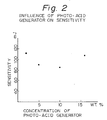
- This example is intended to ascertain the effect of the concentration of the added photo-acid generator on the sensitivity of the resulting resist patterns.
- Example 2 The procedure of Example 1 was repeated except that the photo-acid generator was replaced by different amounts of 2-(N-phenylamino)phenyldiazonium sulfate.
- the amount of the photo-acid generator added was varied from 2% by weight to 16% by weight.
- the results plotted in Fig. 2 show that all of the resist samples have a good sensitivity of 85 to 110 mJ, but it was observed that the amount of the photo-acid generator should not be less than 2% by weight, as otherwise there is a lowering of the resist retention percentage in the exposed area as a result of insufficient photo-acid generator being present for insolubilizing the resist with respect to water.
- the amount of the photo-acid generator should not be more than 10% by weight, as otherwise foaming will occur in the exposed area of the resist as a result of an incorporation of nitrogen (N2) gas generated therein upon exposure to pattering radiation
- Example 1 The procedure of Example 1 was repeated except that the resist material was replaced by a commercially available novolac resin resist: OFPR-800 (product of Tokyo Oka Kogyo KK), and an excimer laser was used as an exposure source, whereby negative resist patterns having a resolution of 2.0 ⁇ m l&s or more are obtained.
- OFPR-800 product of Tokyo Oka Kogyo KK
Abstract
Description
- The present invention relates to a resist technology, and more particularly, to a pattern-forming resist material suitable for forming negative resist patterns using deep ultraviolet (UV) radiation as an exposure radiation. The resist patterns are usually formed on a substrate or base material, i.e., a semiconductor material, during the production of semiconductor devices such as large-scale integrated (LSI) circuits, very-large-scale integrated (VLSI) circuits, and bubble memory devices. The present invention also relates to a process for the formation of resist patterns using said resist material.
- To attain a desired fine fabrication in the production of LSIs, VLSIs and other semiconductor devices, a plurality of pattern-forming resist materials such as rubber-like resists, photocomposable polymeric resists and novolac resin resists, as well as different exposure radiations such as ultraviolet (UV) rays, electron beams, X-rays, and ion beams, are widely used. Recently, deep UV radiation has replaced the usual UV radiation, as the deep UV radiation has a wavelength of about 200 to 300 nm, which is shorter than that of the usual UV radiation, and can satisfy the requirements for a greater a degree of fine fabrication in the resulting resist patterns. Note, it is known that various intensive research projects and development of deep UV resists have been carried out by persons skilled in the art, and in this connection, as suitable deep UV resists, it has been proposed to use photodecomposable polymeric resins, or novolac resists, which are well known as the UV resists and can be used without modification. These deep UV resists, however, have several drawbacks; the photo decomposable polymeric resins have a poor sensitivity to deep UV and a resistance to dry etching such as oxygen plasma etching, and the novolac resists show an unsatisfactory pattern resolution due to an excessively high light absorption of the benzene ring included therein.
- In addition to these resists, it has been proposed to use cross-linking resists wherein a cross-linkable polymer such as polyvinyl alcohol is combined with a cross-linking agent such as diazonium salts, but these resists have an unsatisfactory pattern resolution due to swelling of the resulting resist patterns. The reason for the swelling of the resist patterns is as follows:
- When a water-soluble polyvinyl alcohol (PVA) of the formula:


- An object of the present invention is to provide a novel pattern-forming resist material particularly suitable for deep UV exposure and formation of fine negative resist patterns having a high sensitivity, a resistance to dry etching, and a good resolution.
- Another object of the present invention is to provide a novel process for the formation of resist patterns, in which the problem of swelling of the patterns due to absorption of water used during development is eliminated.
- According to the present invention, there is provided a pattern-forming resist material comprising a mixture of a water-soluble polymeric material having at least one hydroxyl group in the molecular structure thereof and a photo-acid generator which, during exposure to radiation, does not cause cross-linking of said polymeric material, but releases an acid upon reaction with said polymeric material, the product of reacting the thus reacted polymeric material with said acid on heating in the presence of said acid as catalyst providing a water-insoluble polymeric material as a result of removal of water from said reacted polymeric material, which dewatered polymeric material, when present as a substrate, if said exposure has been to patterning radiation, then provides resist patterns when developed with water.
- According to the present invention there is also provided a process for the formation of a resist pattern, comprising coating a solution of a resist material according to the invention onto a substrate to form a resist layer, exposing said resist layer to patterning radiation to cause reaction of said polymeric material and said photo-acid generator and release of said acid, heating the exposed resist layer in the presence of said acid as a catalyst to remove water from the thus reacted polymeric material in said resist layer, thereby insolubilizing said reaction product in water, and developing said resist layer with water to remove said water-soluble polymeric material in unexposed areas of said layer to form resist patterns on said substrate.
- In the description of the invention which follows, reference will be made to the accompanying drawings, wherein:
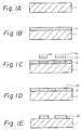
- Figures 1A to 1E are cross-sectional views showing, in sequence, the steps of its pattern formation process according to the present invention; and,
- Fig. 2 is a graph showing the relationship between the sensitivity of the resist material and the concentration of the photo-acid generator, 2-(N-phenylamino) phenyldiazonium sulfate, in the resist material containing PVA as the polymeric material.
- Using the resist material according to the present invention the resist patterns are formed as follows, for example:
- As illustrated in Fig. 1A, a
semiconductor substrate 1, for example, a silicon substrate or wafer, is prepared and washed to obtain clean surfaces. Although not shown, thesubstrate 1 may carry any circuit parts or other elements, if desired; for example, an insulating layer such as SiO₂ layer, circuits such as Al circuits, and the like. - A resist material to be coated on the cleaned surface of the
substrate 1 is prepared by mixing a water-soluble, hydroxyl group-containing polymeric material with a photo-acid generator, i.e., a compound capable of photographically producing and releasing an acid as a result of radiation exposure of the resist material. Here, PVA of the formula:

- After preparation of the resist material, then, as illustrated in Fig. 1B, the resist material is coated on the
substrate 1 to form aresist layer 2. Since this polymeric material has a good solubility in water, coating is generally carried out by conventional coating methods such as spin coating using an aqueous solution of the resist material, and the coated resist material is then dried. - The resulting
resist layer 2 is then selectively exposed to patterning radiation (deep UV used herein) hν through a mask (not shown), as illustrated in Fig. 1C. The wavelength of the deep UV may be a commonly used one, i.e., 240 to 250 nm. During the selective exposure, the following reaction proceeds in the exposed area of the resist layer 2:
- The above reaction schema shows that, during the exposure step, an acid HX₁ such as HCl is generated but no cross-linking reaction occurs. This contrasts with a cross-linking reaction which can be found in the prior art cross-linking resists as previously described (Note: such a cross-linking reaction results in a swelling of the resist patterns). In Fig. 1C, the exposed area of the
resist layer 2 contains areaction product 12 of the PVA and diazonium salt (see, above equation ), but the unexposed area thereof contains the unreacted PVA and diazonium salt. - After selective exposure, the exposed resist layer is then heated to a temperature of, for example, about 100°C, and during this heating, the following reaction proceeds in the exposed area of the
resist layer 2.
product 22 in the exposed area of theresist layer 2 now shows an insolubility in water (see, Fig. 1D). Namely, the exposed area is insolubilized in water, but the unexposed area remains water-soluble. - After the exposed area is insolubilized in water, the resist layer is developed with water to wash the unexposed area therefrom, and as shown in Fig. 1E, water-insoluble
negative resist patterns 22 are thus formed on thesubstrate 1. - According to the present invention, since the formation of the resist patterns involves utilizing variations in the polarity of the resist material used, in contrast with the prior art resist material which is cross-linked upon patterning exposure to form resist patterns, the resulting resist patterns do not suffer from swelling thereof, with the result that these resist patterns are very fine or have an increased resolution. Further, since the acid generated in the exposure step is used as a catalyst in the next reaction, the precursor thereof, i.e., the photo-acid generator, gives satisfactory effects, even if used in a small amount of 10% by weight or less. Furthermore, since a resist material having a small amount of the photo-acid generator incorporated therein has a good transparency to deep UV. The loss of resolution caused by excessively high light absorption such as in the prior art novolac resists is eliminated.
- The pattern-forming resist material according to the present invention comprises a water-soluble polymeric material, as a basic polymer, and a photo-acid generator. Preferably, the polymeric material does not have an aromatic ring such as benzene ring in the molecular structure thereof, as an aromatic ring-free polymeric material ensures the formation of fine resist patterns, because it does not suffer from the reduced resolution caused by specific absorption characteristics of the aromatic ring. Further, preferably the polymeric material has a structure in which a carbon atom adjacent to another carbon atom to which the hydroxyl group is bonded in the polymeric material contains at least one hydrogen atom which can be combined with the split-off hydroxyl group during the heating step to form water, which is then removed from the polymeric material.
- The polymeric material used in the present invention may have a wide range of molecular weights, and a suitable range of the molecular weights thereof is generally from 1,000 to 100,000, although molecular weights over or under that range also may be applied to the polymeric material, insofar as they do not have an adverse affect on the resulting resist patterns.
- The hydroxyl-containing polymeric material used in the present invention may be optionally selected from a plurality of well-known hydroxyl polymers which satisfy the requirements described herein. These polymeric materials include, for example, polyvinyl alcohol (PVA) or derivatives thereof such as poly(1-methyl) thereof such as cellulose esters (for example, cellulose acetate and nitrocellulose) and cellulose ethers (for example, methyl cellulose and ethyl cellulose).
- These polymeric materials may be used alone or in combinations thereof.
- The photo-acid generator used together with the polymeric material, as previously described, is a compound capable of releasing an acid upon exposure to patterning radiation, but this compound does not cause a cross-linking of the polymeric material used at the same time during the exposure step. Any photo-acid generator may be used in the practice of the present invention, insofar as it satisfies the requirements described herein. These photo-acid generators include, for example, an onium salt or compound or derivatives thereof such as ammonium compounds, phosphonium compounds, oxonium compounds, sulfonium compounds and iodonium compounds (for example, p-(N-phenylamino)phenyldiazonium sulfate, 2-(N-phenylamino)phenyldiazonium sulfate, diphenyliodonium trifluoromethane sulfonate and triphenylsulfonium hexafluoroarsenate). Preferred photo-acid generators include those represented by the formula:

Ar may be the same or different and represents a substituted or unsubstituted aromatic group such as a phenyl group, and
X⁻ represents BF₄⁻ SbF₆⁻, PF₆⁻ or AsF₆⁻; and the compounds of formula:
- In the practice of the present invention, the amount used of the photo-acid generator is such that the water-insoluble polymeric material is obtained thereby. The present inventor found that a relatively small amount of the photo-acid generator will provide the desired effects, when used in the present invention, and is usually within the range of about 2 to 10% by weight based on a combined weight of the polymeric material and photo-acid generator.
- The formation of the resist patterns has been described with reference to Figs. 1A to 1E, but, it should be noted that modifications and improvements may be made to the described pattern formation process within the scope and spirit of the present invention.
- In the exposure step of the present process, the patterning radiation is preferably a deep UV radiation pattern having a wavelength of about 200 to 300 nm. The deep UV radiation may be generated from radiation sources such as a Xe-Hg (xenon-mercury vapor) lamp and an excimer laser (wavelength of 248 nm). In addition to the deep UV, other radiations such as electron beams, X-rays and ion beams may be used if desired and if not adversely affecting the patterning process and results thereof.
- The resist material and pattern formation process of the present invention may be widely used to form negative resist patterns with excellent properties, and the thus formed resist patterns may be advantageously utilized in the production of semiconductor devices such as LSI and VLSI, and further may be utilized in the production of photoprinting plates and other articles, if desired.
- The present invention will be further described with reference to following working examples and comparative examples:
- Polyvinyl alcohol (PVA) having a molecular weight of 27,000 was mixed with 5% by weight, based on a total weight of the mixture, of p-(N-phenylamino)phenyldiazonium sulfate as the photo-acid generator and water. The thus obtained aqueous solution of the resist was spun-coated on a silicon wafer, and then dried at 60 °C for 60 minutes, and a resist layer having a layer thickness of 1.0 µm was obtained. The resist layer was exposed to a deep UV radiation pattern (4 mW/cm²) for about 15 seconds, after a wavelength of the radiation from an Xe-Hg lamp was adjusted to below 330 nm by a cold mirror. The exposed resist layer was heated at 100°C for 45 minutes on a hot plate, to insolubilize the exposed area thereof, and after the heating was completed, the resist layer was developed with water to wash the unexposed area therefrom, whereby fine negative resist patterns having a resolution of 1.0 µm l&s (line & space) were obtained. The sensitivity was 90 mJ. It was observed that the resist patterns had a good resistance to oxygen plasma etching.
- The procedure of Example 1 was repeated except that the photo-acid generator was replaced by the same amount of diphenyliodonium trifluoromethane sulfonate. Fine negative resist patterns having a resolution of 0.8 µm l&s and a
sensitivity 120 mJ were obtained. It was observed that the resist patterns had a good resistance to oxygen plasma etching. - The procedure of Example 1 was repeated except that the photo-acid generator was replaced by the same amount of triphenylsulfonium hexafluoroarsenate. Fine negative resist patterns having a resolution of 0.8 µm l&s and a sensitivity of 100 mJ were obtained. It was observed that the resist patterns had a good resistance to oxygen plasma etching.
- The procedure of Example 1 was repeated except that PVA was replaced by methyl cellulose (MC) having a molecular weight of 10,000, and the photo-acid generator was replaced by the same amount of 2-(N-phenylamino)phenyldiazonium sulfate. Fine negative resist patterns having a resolution of 1.5 µm l&s and a sensitivity of 90 mJ were obtained. It was observed that the resist patterns had a good resistance to oxygen plasma etching.
- The procedure of Example 1 was repeated except that PVA was replaced by poly(1-methyl) vinyl alcohol having a molecular weight of 20,000, and the photo-acid generator was replaced by the same amount of 2-(N-phenylamino)phenyldiazonium sulfate. Fine negative resist patterns having a resolution of 1.0 µm l&s and a sensitivity of 90 mJ were obtained. It was observed that the resist patterns had a good resistance to oxygen plasma etching.
- This example is intended to ascertain the effect of the concentration of the added photo-acid generator on the sensitivity of the resulting resist patterns.
- The procedure of Example 1 was repeated except that the photo-acid generator was replaced by different amounts of 2-(N-phenylamino)phenyldiazonium sulfate. The amount of the photo-acid generator added was varied from 2% by weight to 16% by weight. The results plotted in Fig. 2 show that all of the resist samples have a good sensitivity of 85 to 110 mJ, but it was observed that the amount of the photo-acid generator should not be less than 2% by weight, as otherwise there is a lowering of the resist retention percentage in the exposed area as a result of insufficient photo-acid generator being present for insolubilizing the resist with respect to water. Similarly, the amount of the photo-acid generator should not be more than 10% by weight, as otherwise foaming will occur in the exposed area of the resist as a result of an incorporation of nitrogen (N₂) gas generated therein upon exposure to pattering radiation
- The procedure of Example 1 was repeated except that the resist material was replaced by a commercially available novolac resin resist: OFPR-800 (product of Tokyo Oka Kogyo KK), and an excimer laser was used as an exposure source, whereby negative resist patterns having a resolution of 2.0 µm l&s or more are obtained.
- To improve the resolution, the process conditions of the above procedure were varied, but due to insufficient light absorption, the resulting resist patterns showed an unacceptable trapezoid cross-section.
Claims (14)

Ar may be the same or different and represents a substituted or unsubstituted aromatic group, and
X⁻ represents BF₄⁻ , SbF₆⁻ or AsF₆⁻.

Applications Claiming Priority (2)
| Application Number | Priority Date | Filing Date | Title |
|---|---|---|---|
| JP59328/88 | 1988-03-15 | ||
| JP63059328A JPH01233443A (en) | 1988-03-15 | 1988-03-15 | Pattern forming method |
Publications (2)
| Publication Number | Publication Date |
|---|---|
| EP0333407A2 true EP0333407A2 (en) | 1989-09-20 |
| EP0333407A3 EP0333407A3 (en) | 1992-07-01 |
Family
ID=13110167
Family Applications (1)
| Application Number | Title | Priority Date | Filing Date |
|---|---|---|---|
| EP19890302448 Ceased EP0333407A3 (en) | 1988-03-15 | 1989-03-13 | Resist material and process for information of resist patterns |
Country Status (4)
| Country | Link |
|---|---|
| US (1) | US5017461A (en) |
| EP (1) | EP0333407A3 (en) |
| JP (1) | JPH01233443A (en) |
| KR (1) | KR910005884B1 (en) |
Cited By (6)
| Publication number | Priority date | Publication date | Assignee | Title |
|---|---|---|---|---|
| US5550008A (en) * | 1993-05-31 | 1996-08-27 | Sony Corporation | Method for making a dry etching resistant positive and negative photoresist |
| WO2003069382A1 (en) * | 2002-02-12 | 2003-08-21 | 3M Innovative Properties Company | Process for preparing a k-type polarizer |
| US6814899B2 (en) | 2002-02-12 | 2004-11-09 | 3M Innovative Properties Company | Enhanced K-type polarizer |
| US6949207B2 (en) | 2002-04-04 | 2005-09-27 | 3M Innovative Properties Company | K-type polarizer and preparation thereof |
| US7087194B2 (en) | 2002-04-04 | 2006-08-08 | 3M Innovative Properties Company | K-type polarizer and preparation thereof |
| WO2006113492A2 (en) * | 2005-04-14 | 2006-10-26 | President And Fellows Of Harvard College | Adjustable solubility in sacrificial layers for microfabrication |
Families Citing this family (50)
| Publication number | Priority date | Publication date | Assignee | Title |
|---|---|---|---|---|
| US5252435A (en) * | 1990-01-30 | 1993-10-12 | Matsushita Electric Industrial Co., Ltd. | Method for forming pattern |
| US5691101A (en) * | 1994-03-15 | 1997-11-25 | Kabushiki Kaisha Toshiba | Photosensitive composition |
| US6905621B2 (en) * | 2002-10-10 | 2005-06-14 | Taiwan Semiconductor Manufacturing Co., Ltd. | Method for preventing the etch transfer of sidelobes in contact hole patterns |
| US7235348B2 (en) * | 2003-05-22 | 2007-06-26 | Taiwan Semiconductor Manufacturing Co., Ltd. | Water soluble negative tone photoresist |
| US7033735B2 (en) * | 2003-11-17 | 2006-04-25 | Taiwan Semiconductor Manufacturing Co., Ltd. | Water soluble negative tone photoresist |
| JP4196822B2 (en) * | 2003-12-22 | 2008-12-17 | パナソニック株式会社 | Water-soluble material and pattern forming method using the same |
| US7651830B2 (en) * | 2007-06-01 | 2010-01-26 | 3M Innovative Properties Company | Patterned photoacid etching and articles therefrom |
| JP6423801B2 (en) | 2013-02-12 | 2018-11-14 | カーボン,インコーポレイテッド | Method and apparatus for three-dimensional fabrication |
| CN105452958B (en) | 2013-02-12 | 2020-03-20 | 卡本有限公司 | Method and apparatus for three-dimensional fabrication with feed through carrier |
| WO2015142546A1 (en) | 2014-03-21 | 2015-09-24 | Carbon3D, Inc. | Method and apparatus for three-dimensional fabrication with gas injection through carrier |
| EP3656559A1 (en) | 2014-04-25 | 2020-05-27 | Carbon, Inc. | Continuous three dimensional fabrication from immiscible liquids |
| US10661501B2 (en) | 2014-06-20 | 2020-05-26 | Carbon, Inc. | Three-dimensional printing method using increased light intensity and apparatus therefor |
| US10569465B2 (en) | 2014-06-20 | 2020-02-25 | Carbon, Inc. | Three-dimensional printing using tiled light engines |
| KR20170017941A (en) | 2014-06-20 | 2017-02-15 | 카본, 인크. | Three-dimensional printing with reciprocal feeding of polymerizable liquid |
| BR112016029793A2 (en) | 2014-06-23 | 2017-08-22 | Carbon Inc | polyurethane resins having multiple hardening mechanisms for use in the production of three dimensional objects |
| US11390062B2 (en) | 2014-08-12 | 2022-07-19 | Carbon, Inc. | Three-dimensional printing with supported build plates |
| EP3240671B1 (en) | 2014-12-31 | 2020-12-16 | Carbon, Inc. | Three-dimensional printing of objects with breathing orifices |
| WO2016112084A1 (en) | 2015-01-06 | 2016-07-14 | Carbon3D, Inc. | Build plate for three dimensional printing having a rough or patterned surface |
| WO2016112090A1 (en) | 2015-01-07 | 2016-07-14 | Carbon3D, Inc. | Microfluidic devices and methods of making the same |
| EP3245044B1 (en) | 2015-01-13 | 2021-05-05 | Carbon, Inc. | Three-dimensional printing with build plates having surface topologies for increasing permeability and related methods |
| US11020898B2 (en) | 2015-01-30 | 2021-06-01 | Carbon, Inc. | Build plates for continuous liquid interface printing having permeable base and adhesive for increasing permeability and related methods, systems and devices |
| EP3250368A1 (en) | 2015-01-30 | 2017-12-06 | Carbon, Inc. | Build plates for continuous liquid interface printing having permeable sheets and related methods, systems and devices |
| EP3253558B1 (en) | 2015-02-05 | 2020-04-08 | Carbon, Inc. | Method of additive manufacturing by fabrication through multiple zones |
| US11000992B2 (en) | 2015-02-20 | 2021-05-11 | Carbon, Inc. | Methods and apparatus for continuous liquid interface printing with electrochemically supported dead zone |
| WO2016140888A1 (en) | 2015-03-05 | 2016-09-09 | Carbon3D, Inc. | Fabrication of three dimensional objects with variable slice thickness |
| US20180029292A1 (en) | 2015-03-05 | 2018-02-01 | Carbon, Inc. | Continuous liquid interface production with sequential patterned exposure |
| WO2016140886A1 (en) | 2015-03-05 | 2016-09-09 | Carbon3D, Inc. | Fabrication of three dimensional objects with multiple operating modes |
| WO2016145050A1 (en) | 2015-03-10 | 2016-09-15 | Carbon3D, Inc. | Microfluidic devices having flexible features and methods of making the same |
| WO2016145182A1 (en) | 2015-03-12 | 2016-09-15 | Carbon3D, Inc. | Additive manufacturing using polymerization initiators or inhibitors having controlled migration |
| US10843402B2 (en) | 2015-03-13 | 2020-11-24 | Carbon, Inc. | Three-dimensional printing with reduced pressure build plate unit |
| WO2016149151A1 (en) | 2015-03-13 | 2016-09-22 | Carbon3D, Inc. | Three-dimensional printing with concurrent delivery of different polymerizable liquids |
| US10792856B2 (en) | 2015-03-13 | 2020-10-06 | Carbon, Inc. | Three-dimensional printing with flexible build plates |
| US10800094B2 (en) | 2015-09-14 | 2020-10-13 | Carbon, Inc. | Light-curable article of manufacture with portions of differing solubility |
| CN108367495B (en) | 2015-09-25 | 2021-06-15 | 卡本有限公司 | Build plate assembly with light emitting panel for continuous liquid interphase printing and related methods, systems, and devices |
| WO2017059082A1 (en) | 2015-09-30 | 2017-04-06 | Carbon, Inc. | Method and apparatus for producing three-dimensional objects |
| US10647873B2 (en) | 2015-10-30 | 2020-05-12 | Carbon, Inc. | Dual cure article of manufacture with portions of differing solubility |
| US10647054B2 (en) | 2015-12-22 | 2020-05-12 | Carbon, Inc. | Accelerants for additive manufacturing with dual cure resins |
| WO2017112571A1 (en) | 2015-12-22 | 2017-06-29 | Carbon, Inc. | Dual cure additive manufacturing of rigid intermediates that generate semi-rigid, flexible, or elastic final products |
| JP6944935B2 (en) | 2015-12-22 | 2021-10-06 | カーボン,インコーポレイテッド | Manufacture of composite products from multiple intermediates by laminated molding using double-cured resin |
| WO2017112521A1 (en) | 2015-12-22 | 2017-06-29 | Carbon, Inc. | Production of flexible products by additive manufacturing with dual cure resins |
| EP3341792A1 (en) | 2015-12-22 | 2018-07-04 | Carbon, Inc. | Dual precursor resin systems for additive manufacturing with dual cure resins |
| EP3463820A4 (en) | 2016-05-31 | 2020-04-08 | Northwestern University | Method for the fabrication of three-dimensional objects and apparatus for same |
| US11014299B2 (en) | 2016-07-01 | 2021-05-25 | Carbon, Inc. | Three-dimensional printing with build plates having reduced pressure and/or channels for increased fluid flow |
| US11135790B2 (en) | 2016-11-21 | 2021-10-05 | Carbon, Inc. | Method of making three-dimensional object by delivering reactive component for subsequent cure |
| US10239255B2 (en) | 2017-04-11 | 2019-03-26 | Molecule Corp | Fabrication of solid materials or films from a polymerizable liquid |
| US11720017B2 (en) * | 2017-04-18 | 2023-08-08 | The University Of Chicago | Photoactive, inorganic ligand-capped inorganic nanocrystals |
| NL2022372B1 (en) | 2018-12-17 | 2020-07-03 | What The Future Venture Capital Wtfvc B V | Process for producing a cured 3d product |
| SG11202110863TA (en) | 2019-04-09 | 2021-10-28 | Azul 3D Inc | Methodologies to rapidly cure and coat parts produced by additive manufacturing |
| CN113745439B (en) * | 2020-05-27 | 2023-04-18 | 京东方科技集团股份有限公司 | Quantum dot light-emitting structure, manufacturing method thereof and display device |
| CN114784151A (en) * | 2022-03-22 | 2022-07-22 | 清华大学 | Method for printing nanoparticles and light-emitting element |
Citations (4)
| Publication number | Priority date | Publication date | Assignee | Title |
|---|---|---|---|---|
| GB501069A (en) * | 1937-06-18 | 1939-02-21 | Harris Seybold Potter Co | An improved process for the preparation of lithographic plates for printing |
| US4341859A (en) * | 1980-09-23 | 1982-07-27 | General Electric Company | Emulsion for making dry film resists |
| US4610952A (en) * | 1983-09-14 | 1986-09-09 | General Electric Company | Photoresist compositions and method |
| US4657844A (en) * | 1983-06-27 | 1987-04-14 | Texas Instruments Incorporated | Plasma developable negative resist compositions for electron beam, X-ray and optical lithography |
Family Cites Families (4)
| Publication number | Priority date | Publication date | Assignee | Title |
|---|---|---|---|---|
| US4414059A (en) * | 1982-12-09 | 1983-11-08 | International Business Machines Corporation | Far UV patterning of resist materials |
| US4537854A (en) * | 1983-09-14 | 1985-08-27 | General Electric Company | Photoresist compositions and method |
| EP0195106B1 (en) * | 1985-03-22 | 1989-06-21 | Ibm Deutschland Gmbh | Lift-off mask production process and use of the mask |
| DE3721741A1 (en) * | 1987-07-01 | 1989-01-12 | Basf Ag | RADIATION-SENSITIVE MIXTURE FOR LIGHT-SENSITIVE COATING MATERIALS |
-
1988
- 1988-03-15 JP JP63059328A patent/JPH01233443A/en active Pending
-
1989
- 1989-03-13 US US07/322,037 patent/US5017461A/en not_active Expired - Fee Related
- 1989-03-13 EP EP19890302448 patent/EP0333407A3/en not_active Ceased
- 1989-03-15 KR KR1019890003188A patent/KR910005884B1/en not_active IP Right Cessation
Patent Citations (4)
| Publication number | Priority date | Publication date | Assignee | Title |
|---|---|---|---|---|
| GB501069A (en) * | 1937-06-18 | 1939-02-21 | Harris Seybold Potter Co | An improved process for the preparation of lithographic plates for printing |
| US4341859A (en) * | 1980-09-23 | 1982-07-27 | General Electric Company | Emulsion for making dry film resists |
| US4657844A (en) * | 1983-06-27 | 1987-04-14 | Texas Instruments Incorporated | Plasma developable negative resist compositions for electron beam, X-ray and optical lithography |
| US4610952A (en) * | 1983-09-14 | 1986-09-09 | General Electric Company | Photoresist compositions and method |
Cited By (11)
| Publication number | Priority date | Publication date | Assignee | Title |
|---|---|---|---|---|
| US5550008A (en) * | 1993-05-31 | 1996-08-27 | Sony Corporation | Method for making a dry etching resistant positive and negative photoresist |
| WO2003069382A1 (en) * | 2002-02-12 | 2003-08-21 | 3M Innovative Properties Company | Process for preparing a k-type polarizer |
| US6808657B2 (en) | 2002-02-12 | 2004-10-26 | 3M Innovative Properties Company | Process for preparing a K-type polarizer |
| US6814899B2 (en) | 2002-02-12 | 2004-11-09 | 3M Innovative Properties Company | Enhanced K-type polarizer |
| US6998179B2 (en) | 2002-02-12 | 2006-02-14 | 3M Innovative Properties Company | Process for preparing a K-type polarizer |
| CN1311256C (en) * | 2002-02-12 | 2007-04-18 | 3M创新有限公司 | Process for preparing a K-type polarizer |
| US6949207B2 (en) | 2002-04-04 | 2005-09-27 | 3M Innovative Properties Company | K-type polarizer and preparation thereof |
| US7087194B2 (en) | 2002-04-04 | 2006-08-08 | 3M Innovative Properties Company | K-type polarizer and preparation thereof |
| WO2006113492A2 (en) * | 2005-04-14 | 2006-10-26 | President And Fellows Of Harvard College | Adjustable solubility in sacrificial layers for microfabrication |
| WO2006113492A3 (en) * | 2005-04-14 | 2006-12-07 | Harvard College | Adjustable solubility in sacrificial layers for microfabrication |
| US8357616B2 (en) | 2005-04-14 | 2013-01-22 | President And Fellows Of Harvard College | Adjustable solubility in sacrificial layers for microfabrication |
Also Published As
| Publication number | Publication date |
|---|---|
| KR890015077A (en) | 1989-10-28 |
| JPH01233443A (en) | 1989-09-19 |
| KR910005884B1 (en) | 1991-08-06 |
| EP0333407A3 (en) | 1992-07-01 |
| US5017461A (en) | 1991-05-21 |
Similar Documents
| Publication | Publication Date | Title |
|---|---|---|
| EP0333407A2 (en) | Resist material and process for information of resist patterns | |
| JP4216705B2 (en) | Photoresist pattern forming method | |
| US5118585A (en) | Positive and negative working radiation sensitive mixtures and production of relief patterns | |
| EP1311908B1 (en) | Photoresist composition for deep uv and process thereof | |
| JP3408415B2 (en) | Antireflection coating composition comprising photoacid generator | |
| JP3723670B2 (en) | Frequency double hybrid photo resist | |
| US6365322B1 (en) | Photoresist composition for deep UV radiation | |
| JP2501292B2 (en) | Method for making acid sensitive polymers and photoresist structures | |
| JP4299670B2 (en) | Negative deep UV photoresist | |
| JP3509988B2 (en) | Radiation-sensitive mixture | |
| JPH1172917A (en) | Negative photoresist composition and method for forming pattern by using the same | |
| JP4136934B2 (en) | Negative-type aqueous photoresist composition | |
| KR100570206B1 (en) | Organic anti-reflective coating polymer, its preparation method and organic anti-reflective coating composition comprising the same | |
| US5814432A (en) | Method of forming patterns for use in manufacturing electronic devices | |
| JPH0547656A (en) | Forming method for resist pattern and organic silane compound for forming reflection preventive film used therefor | |
| KR100520670B1 (en) | A Process for Forming Photoresist Pattern | |
| JP3983658B2 (en) | Organic antireflection coating composition and photoresist pattern forming method using the same | |
| CA2020378A1 (en) | Maleimide containing, negative working deep uv photoresist | |
| EP1295177B1 (en) | Strongly water-soluble photoacid generator resist compositions | |
| JPS6037548A (en) | Plasma developable negative resist compound for electron beam, x ray and optical lithography and manufacture thereof | |
| JPH04358155A (en) | Acid hardening photoresist | |
| Bohland et al. | Some resists based on chemically-amplified crosslinking of phenolic polymers | |
| JPH09134015A (en) | Pattern forming material, pattern forming method and production of semiconductor device | |
| EP0396254A2 (en) | Photosensitive composition and pattern formation method using the same | |
| US6989227B2 (en) | E-beam curable resist and process for e-beam curing the resist |
Legal Events
| Date | Code | Title | Description |
|---|---|---|---|
| PUAI | Public reference made under article 153(3) epc to a published international application that has entered the european phase |
Free format text: ORIGINAL CODE: 0009012 |
|
| AK | Designated contracting states |
Kind code of ref document: A2 Designated state(s): DE FR GB |
|
| PUAL | Search report despatched |
Free format text: ORIGINAL CODE: 0009013 |
|
| AK | Designated contracting states |
Kind code of ref document: A3 Designated state(s): DE FR GB |
|
| 17P | Request for examination filed |
Effective date: 19921013 |
|
| 17Q | First examination report despatched |
Effective date: 19950125 |
|
| GRAG | Despatch of communication of intention to grant |
Free format text: ORIGINAL CODE: EPIDOS AGRA |
|
| STAA | Information on the status of an ep patent application or granted ep patent |
Free format text: STATUS: THE APPLICATION HAS BEEN REFUSED |
|
| 18R | Application refused |
Effective date: 19970306 |