EP0330452A2 - Electrically conductive pressure-sensitive adhesive tape - Google Patents
Electrically conductive pressure-sensitive adhesive tape Download PDFInfo
- Publication number
- EP0330452A2 EP0330452A2 EP89301733A EP89301733A EP0330452A2 EP 0330452 A2 EP0330452 A2 EP 0330452A2 EP 89301733 A EP89301733 A EP 89301733A EP 89301733 A EP89301733 A EP 89301733A EP 0330452 A2 EP0330452 A2 EP 0330452A2
- Authority
- EP
- European Patent Office
- Prior art keywords
- particles
- adhesive
- electrically conductive
- tape
- adhesive tape
- Prior art date
- Legal status (The legal status is an assumption and is not a legal conclusion. Google has not performed a legal analysis and makes no representation as to the accuracy of the status listed.)
- Granted
Links
Images

Classifications
-
- H—ELECTRICITY
- H01—ELECTRIC ELEMENTS
- H01B—CABLES; CONDUCTORS; INSULATORS; SELECTION OF MATERIALS FOR THEIR CONDUCTIVE, INSULATING OR DIELECTRIC PROPERTIES
- H01B1/00—Conductors or conductive bodies characterised by the conductive materials; Selection of materials as conductors
-
- H—ELECTRICITY
- H01—ELECTRIC ELEMENTS
- H01B—CABLES; CONDUCTORS; INSULATORS; SELECTION OF MATERIALS FOR THEIR CONDUCTIVE, INSULATING OR DIELECTRIC PROPERTIES
- H01B1/00—Conductors or conductive bodies characterised by the conductive materials; Selection of materials as conductors
- H01B1/20—Conductive material dispersed in non-conductive organic material
- H01B1/22—Conductive material dispersed in non-conductive organic material the conductive material comprising metals or alloys
-
- C—CHEMISTRY; METALLURGY
- C09—DYES; PAINTS; POLISHES; NATURAL RESINS; ADHESIVES; COMPOSITIONS NOT OTHERWISE PROVIDED FOR; APPLICATIONS OF MATERIALS NOT OTHERWISE PROVIDED FOR
- C09J—ADHESIVES; NON-MECHANICAL ASPECTS OF ADHESIVE PROCESSES IN GENERAL; ADHESIVE PROCESSES NOT PROVIDED FOR ELSEWHERE; USE OF MATERIALS AS ADHESIVES
- C09J7/00—Adhesives in the form of films or foils
- C09J7/20—Adhesives in the form of films or foils characterised by their carriers
-
- C—CHEMISTRY; METALLURGY
- C09—DYES; PAINTS; POLISHES; NATURAL RESINS; ADHESIVES; COMPOSITIONS NOT OTHERWISE PROVIDED FOR; APPLICATIONS OF MATERIALS NOT OTHERWISE PROVIDED FOR
- C09J—ADHESIVES; NON-MECHANICAL ASPECTS OF ADHESIVE PROCESSES IN GENERAL; ADHESIVE PROCESSES NOT PROVIDED FOR ELSEWHERE; USE OF MATERIALS AS ADHESIVES
- C09J9/00—Adhesives characterised by their physical nature or the effects produced, e.g. glue sticks
- C09J9/02—Electrically-conducting adhesives
-
- H—ELECTRICITY
- H01—ELECTRIC ELEMENTS
- H01R—ELECTRICALLY-CONDUCTIVE CONNECTIONS; STRUCTURAL ASSOCIATIONS OF A PLURALITY OF MUTUALLY-INSULATED ELECTRICAL CONNECTING ELEMENTS; COUPLING DEVICES; CURRENT COLLECTORS
- H01R4/00—Electrically-conductive connections between two or more conductive members in direct contact, i.e. touching one another; Means for effecting or maintaining such contact; Electrically-conductive connections having two or more spaced connecting locations for conductors and using contact members penetrating insulation
- H01R4/04—Electrically-conductive connections between two or more conductive members in direct contact, i.e. touching one another; Means for effecting or maintaining such contact; Electrically-conductive connections having two or more spaced connecting locations for conductors and using contact members penetrating insulation using electrically conductive adhesives
-
- H—ELECTRICITY
- H05—ELECTRIC TECHNIQUES NOT OTHERWISE PROVIDED FOR
- H05K—PRINTED CIRCUITS; CASINGS OR CONSTRUCTIONAL DETAILS OF ELECTRIC APPARATUS; MANUFACTURE OF ASSEMBLAGES OF ELECTRICAL COMPONENTS
- H05K3/00—Apparatus or processes for manufacturing printed circuits
- H05K3/30—Assembling printed circuits with electric components, e.g. with resistor
- H05K3/32—Assembling printed circuits with electric components, e.g. with resistor electrically connecting electric components or wires to printed circuits
- H05K3/321—Assembling printed circuits with electric components, e.g. with resistor electrically connecting electric components or wires to printed circuits by conductive adhesives
- H05K3/323—Assembling printed circuits with electric components, e.g. with resistor electrically connecting electric components or wires to printed circuits by conductive adhesives by applying an anisotropic conductive adhesive layer over an array of pads
-
- H—ELECTRICITY
- H05—ELECTRIC TECHNIQUES NOT OTHERWISE PROVIDED FOR
- H05K—PRINTED CIRCUITS; CASINGS OR CONSTRUCTIONAL DETAILS OF ELECTRIC APPARATUS; MANUFACTURE OF ASSEMBLAGES OF ELECTRICAL COMPONENTS
- H05K3/00—Apparatus or processes for manufacturing printed circuits
- H05K3/36—Assembling printed circuits with other printed circuits
- H05K3/368—Assembling printed circuits with other printed circuits parallel to each other
-
- H—ELECTRICITY
- H05—ELECTRIC TECHNIQUES NOT OTHERWISE PROVIDED FOR
- H05K—PRINTED CIRCUITS; CASINGS OR CONSTRUCTIONAL DETAILS OF ELECTRIC APPARATUS; MANUFACTURE OF ASSEMBLAGES OF ELECTRICAL COMPONENTS
- H05K2201/00—Indexing scheme relating to printed circuits covered by H05K1/00
- H05K2201/02—Fillers; Particles; Fibers; Reinforcement materials
- H05K2201/0203—Fillers and particles
- H05K2201/0206—Materials
- H05K2201/0221—Insulating particles having an electrically conductive coating
-
- H—ELECTRICITY
- H05—ELECTRIC TECHNIQUES NOT OTHERWISE PROVIDED FOR
- H05K—PRINTED CIRCUITS; CASINGS OR CONSTRUCTIONAL DETAILS OF ELECTRIC APPARATUS; MANUFACTURE OF ASSEMBLAGES OF ELECTRICAL COMPONENTS
- H05K2201/00—Indexing scheme relating to printed circuits covered by H05K1/00
- H05K2201/02—Fillers; Particles; Fibers; Reinforcement materials
- H05K2201/0203—Fillers and particles
- H05K2201/0206—Materials
- H05K2201/023—Hard particles, i.e. particles in conductive adhesive at least partly penetrating an electrode
-
- H—ELECTRICITY
- H05—ELECTRIC TECHNIQUES NOT OTHERWISE PROVIDED FOR
- H05K—PRINTED CIRCUITS; CASINGS OR CONSTRUCTIONAL DETAILS OF ELECTRIC APPARATUS; MANUFACTURE OF ASSEMBLAGES OF ELECTRICAL COMPONENTS
- H05K2201/00—Indexing scheme relating to printed circuits covered by H05K1/00
- H05K2201/09—Shape and layout
- H05K2201/09818—Shape or layout details not covered by a single group of H05K2201/09009 - H05K2201/09809
- H05K2201/09945—Universal aspects, e.g. universal inner layers or via grid, or anisotropic interposer
-
- H—ELECTRICITY
- H05—ELECTRIC TECHNIQUES NOT OTHERWISE PROVIDED FOR
- H05K—PRINTED CIRCUITS; CASINGS OR CONSTRUCTIONAL DETAILS OF ELECTRIC APPARATUS; MANUFACTURE OF ASSEMBLAGES OF ELECTRICAL COMPONENTS
- H05K2201/00—Indexing scheme relating to printed circuits covered by H05K1/00
- H05K2201/10—Details of components or other objects attached to or integrated in a printed circuit board
- H05K2201/10227—Other objects, e.g. metallic pieces
- H05K2201/10234—Metallic balls
-
- H—ELECTRICITY
- H05—ELECTRIC TECHNIQUES NOT OTHERWISE PROVIDED FOR
- H05K—PRINTED CIRCUITS; CASINGS OR CONSTRUCTIONAL DETAILS OF ELECTRIC APPARATUS; MANUFACTURE OF ASSEMBLAGES OF ELECTRICAL COMPONENTS
- H05K2203/00—Indexing scheme relating to apparatus or processes for manufacturing printed circuits covered by H05K3/00
- H05K2203/02—Details related to mechanical or acoustic processing, e.g. drilling, punching, cutting, using ultrasound
- H05K2203/0278—Flat pressure, e.g. for connecting terminals with anisotropic conductive adhesive
-
- H—ELECTRICITY
- H05—ELECTRIC TECHNIQUES NOT OTHERWISE PROVIDED FOR
- H05K—PRINTED CIRCUITS; CASINGS OR CONSTRUCTIONAL DETAILS OF ELECTRIC APPARATUS; MANUFACTURE OF ASSEMBLAGES OF ELECTRICAL COMPONENTS
- H05K2203/00—Indexing scheme relating to apparatus or processes for manufacturing printed circuits covered by H05K3/00
- H05K2203/03—Metal processing
- H05K2203/0338—Transferring metal or conductive material other than a circuit pattern, e.g. bump, solder, printed component
-
- H—ELECTRICITY
- H05—ELECTRIC TECHNIQUES NOT OTHERWISE PROVIDED FOR
- H05K—PRINTED CIRCUITS; CASINGS OR CONSTRUCTIONAL DETAILS OF ELECTRIC APPARATUS; MANUFACTURE OF ASSEMBLAGES OF ELECTRICAL COMPONENTS
- H05K3/00—Apparatus or processes for manufacturing printed circuits
- H05K3/36—Assembling printed circuits with other printed circuits
- H05K3/361—Assembling flexible printed circuits with other printed circuits
-
- Y—GENERAL TAGGING OF NEW TECHNOLOGICAL DEVELOPMENTS; GENERAL TAGGING OF CROSS-SECTIONAL TECHNOLOGIES SPANNING OVER SEVERAL SECTIONS OF THE IPC; TECHNICAL SUBJECTS COVERED BY FORMER USPC CROSS-REFERENCE ART COLLECTIONS [XRACs] AND DIGESTS
- Y10—TECHNICAL SUBJECTS COVERED BY FORMER USPC
- Y10S—TECHNICAL SUBJECTS COVERED BY FORMER USPC CROSS-REFERENCE ART COLLECTIONS [XRACs] AND DIGESTS
- Y10S428/00—Stock material or miscellaneous articles
- Y10S428/906—Roll or coil
-
- Y—GENERAL TAGGING OF NEW TECHNOLOGICAL DEVELOPMENTS; GENERAL TAGGING OF CROSS-SECTIONAL TECHNOLOGIES SPANNING OVER SEVERAL SECTIONS OF THE IPC; TECHNICAL SUBJECTS COVERED BY FORMER USPC CROSS-REFERENCE ART COLLECTIONS [XRACs] AND DIGESTS
- Y10—TECHNICAL SUBJECTS COVERED BY FORMER USPC
- Y10T—TECHNICAL SUBJECTS COVERED BY FORMER US CLASSIFICATION
- Y10T428/00—Stock material or miscellaneous articles
- Y10T428/14—Layer or component removable to expose adhesive
- Y10T428/1424—Halogen containing compound
- Y10T428/1429—Fluorine
-
- Y—GENERAL TAGGING OF NEW TECHNOLOGICAL DEVELOPMENTS; GENERAL TAGGING OF CROSS-SECTIONAL TECHNOLOGIES SPANNING OVER SEVERAL SECTIONS OF THE IPC; TECHNICAL SUBJECTS COVERED BY FORMER USPC CROSS-REFERENCE ART COLLECTIONS [XRACs] AND DIGESTS
- Y10—TECHNICAL SUBJECTS COVERED BY FORMER USPC
- Y10T—TECHNICAL SUBJECTS COVERED BY FORMER US CLASSIFICATION
- Y10T428/00—Stock material or miscellaneous articles
- Y10T428/24—Structurally defined web or sheet [e.g., overall dimension, etc.]
- Y10T428/24355—Continuous and nonuniform or irregular surface on layer or component [e.g., roofing, etc.]
- Y10T428/24372—Particulate matter
- Y10T428/2438—Coated
-
- Y—GENERAL TAGGING OF NEW TECHNOLOGICAL DEVELOPMENTS; GENERAL TAGGING OF CROSS-SECTIONAL TECHNOLOGIES SPANNING OVER SEVERAL SECTIONS OF THE IPC; TECHNICAL SUBJECTS COVERED BY FORMER USPC CROSS-REFERENCE ART COLLECTIONS [XRACs] AND DIGESTS
- Y10—TECHNICAL SUBJECTS COVERED BY FORMER USPC
- Y10T—TECHNICAL SUBJECTS COVERED BY FORMER US CLASSIFICATION
- Y10T428/00—Stock material or miscellaneous articles
- Y10T428/24—Structurally defined web or sheet [e.g., overall dimension, etc.]
- Y10T428/24355—Continuous and nonuniform or irregular surface on layer or component [e.g., roofing, etc.]
- Y10T428/24372—Particulate matter
- Y10T428/24413—Metal or metal compound
-
- Y—GENERAL TAGGING OF NEW TECHNOLOGICAL DEVELOPMENTS; GENERAL TAGGING OF CROSS-SECTIONAL TECHNOLOGIES SPANNING OVER SEVERAL SECTIONS OF THE IPC; TECHNICAL SUBJECTS COVERED BY FORMER USPC CROSS-REFERENCE ART COLLECTIONS [XRACs] AND DIGESTS
- Y10—TECHNICAL SUBJECTS COVERED BY FORMER USPC
- Y10T—TECHNICAL SUBJECTS COVERED BY FORMER US CLASSIFICATION
- Y10T428/00—Stock material or miscellaneous articles
- Y10T428/24—Structurally defined web or sheet [e.g., overall dimension, etc.]
- Y10T428/24479—Structurally defined web or sheet [e.g., overall dimension, etc.] including variation in thickness
- Y10T428/24521—Structurally defined web or sheet [e.g., overall dimension, etc.] including variation in thickness with component conforming to contour of nonplanar surface
- Y10T428/24545—Containing metal or metal compound
-
- Y—GENERAL TAGGING OF NEW TECHNOLOGICAL DEVELOPMENTS; GENERAL TAGGING OF CROSS-SECTIONAL TECHNOLOGIES SPANNING OVER SEVERAL SECTIONS OF THE IPC; TECHNICAL SUBJECTS COVERED BY FORMER USPC CROSS-REFERENCE ART COLLECTIONS [XRACs] AND DIGESTS
- Y10—TECHNICAL SUBJECTS COVERED BY FORMER USPC
- Y10T—TECHNICAL SUBJECTS COVERED BY FORMER US CLASSIFICATION
- Y10T428/00—Stock material or miscellaneous articles
- Y10T428/24—Structurally defined web or sheet [e.g., overall dimension, etc.]
- Y10T428/24802—Discontinuous or differential coating, impregnation or bond [e.g., artwork, printing, retouched photograph, etc.]
- Y10T428/24843—Discontinuous or differential coating, impregnation or bond [e.g., artwork, printing, retouched photograph, etc.] with heat sealable or heat releasable adhesive layer
-
- Y—GENERAL TAGGING OF NEW TECHNOLOGICAL DEVELOPMENTS; GENERAL TAGGING OF CROSS-SECTIONAL TECHNOLOGIES SPANNING OVER SEVERAL SECTIONS OF THE IPC; TECHNICAL SUBJECTS COVERED BY FORMER USPC CROSS-REFERENCE ART COLLECTIONS [XRACs] AND DIGESTS
- Y10—TECHNICAL SUBJECTS COVERED BY FORMER USPC
- Y10T—TECHNICAL SUBJECTS COVERED BY FORMER US CLASSIFICATION
- Y10T428/00—Stock material or miscellaneous articles
- Y10T428/24—Structurally defined web or sheet [e.g., overall dimension, etc.]
- Y10T428/24802—Discontinuous or differential coating, impregnation or bond [e.g., artwork, printing, retouched photograph, etc.]
- Y10T428/24893—Discontinuous or differential coating, impregnation or bond [e.g., artwork, printing, retouched photograph, etc.] including particulate material
-
- Y—GENERAL TAGGING OF NEW TECHNOLOGICAL DEVELOPMENTS; GENERAL TAGGING OF CROSS-SECTIONAL TECHNOLOGIES SPANNING OVER SEVERAL SECTIONS OF THE IPC; TECHNICAL SUBJECTS COVERED BY FORMER USPC CROSS-REFERENCE ART COLLECTIONS [XRACs] AND DIGESTS
- Y10—TECHNICAL SUBJECTS COVERED BY FORMER USPC
- Y10T—TECHNICAL SUBJECTS COVERED BY FORMER US CLASSIFICATION
- Y10T428/00—Stock material or miscellaneous articles
- Y10T428/25—Web or sheet containing structurally defined element or component and including a second component containing structurally defined particles
- Y10T428/256—Heavy metal or aluminum or compound thereof
-
- Y—GENERAL TAGGING OF NEW TECHNOLOGICAL DEVELOPMENTS; GENERAL TAGGING OF CROSS-SECTIONAL TECHNOLOGIES SPANNING OVER SEVERAL SECTIONS OF THE IPC; TECHNICAL SUBJECTS COVERED BY FORMER USPC CROSS-REFERENCE ART COLLECTIONS [XRACs] AND DIGESTS
- Y10—TECHNICAL SUBJECTS COVERED BY FORMER USPC
- Y10T—TECHNICAL SUBJECTS COVERED BY FORMER US CLASSIFICATION
- Y10T428/00—Stock material or miscellaneous articles
- Y10T428/28—Web or sheet containing structurally defined element or component and having an adhesive outermost layer
- Y10T428/2852—Adhesive compositions
- Y10T428/2857—Adhesive compositions including metal or compound thereof or natural rubber
Definitions
- the invention concerns adhesive tape, preferably pressure-sensitive adhesive tape, the adhesive layer of which contains particles affording electrical conductivity through the thickness of the layer while being electrically insulating in lateral directions.
- U.S. Pat. No. 4,113,981 describes a product that uses an adhesive layer for individually electrically interconnecting multiple pairs of arrayed electrodes.
- the adhesive layer includes spherical electrically conductive particles of substantially the same thickness as the adhesive, thus providing a conductive path through each particle that bridges facing pairs of electrodes.
- the particles are randomly distributed throughout the adhesive layer, but U.S. Pat. No. 4,113,981 indicates that if the particles comprise less than 30% by volume of the layer, they will be sufficiently spaced so that the intervening adhesive will insulate against short circuiting between laterally adjacent electrodes. Carbon powder, SiC powder and metal powder are said to be useful.
- U.S. Pat. No. 3,475,213 discloses a tape having an electrically conductive backing and a pressure-sensitive adhesive layer which contains a monolayer of electrically conductive particles that could be identical to the adhesive layer of aforementioned U.S. Pat. No. 4,113,981 if the latter patentee were to use a pressure-sensitive adhesive.
- U.S. Pat. No. 3,475,213 says that the particles should "have a substantial thickness slightly less than the thickness of the adhesive film", and "essentially none of the particles should extend above the surface of the adhesive to preserve satisfactory adhesion values".
- 3,475,213 indicates a preference for metal particles, preferably flattened to appropriate thickness before being added to an adhesive-coating mixture, while also suggesting the use of metallized plastic or glass beads or spheres and that the particles can be metal alloys, or composites in which one metal is coated on another.
- U.S. Pat. No. 4,548,862 concerns a flexible tape that, like the adhesive layer U.S. Pat. No. 4,113,981, can adhesively make individual electrical connections between multiple pairs of electrode arrays without short circuiting electrodes of either array by means of small particles that form electrically conductive bridges extending through the thickness of the layer.
- Each of the particles has a ferromagnetic core and an electrically conductive surface layer such as silver.
- U.S. Pat. No. 4,606,962 like the above-discussed patents, discloses a tape that provides electrical conductivity through the thickness of an adhesive layer, and is especially concerned with adhesively attaching a semiconductor die or chip to a substrate to dissipate both heat and static electricity.
- the adhesive layer of the tape described in this patent which preferably is heat-activatable, contains electrically and thermally conductive particles that at the bonding temperature of the adhesive are at least as deformable as are substantially pure silver spherical particles. The thickness of the particles exceeds the thickness of the adhesive between particles.
- the particles When the particle-containing adhesive layer is removed from the carrier layer of the transfer tape and compressed between two rigid plates, the particles are flattened to the thickness of the adhesive between particles, thus providing small, flat conductive areas at both surfaces of the adhesive layer.
- the particles preferably are substantially spherical and made of a metal such as silver or gold or of more than one material such as a solder surface layer and either a higher melting metal core such as copper or a nonmetallic core.
- the last named patent says that to economize the use of the electrically conductive particles, they may be located only in segments of the novel adhesive transfer tape which are to contact individual electrical conductors.
- One technique suggested by the patentee is to (1) form a viscous adhesive coating, (2) render areas of the coating substantially tack-free, (3) apply electrically conductive particles that adhere only to the viscous portions of the coating, and then (4) polymerize the viscous areas to a substantially tack-free state. When the viscous areas remaining after step (2) are small, the electrically conductive particles are individually positioned in a predetermined pattern.
- the present invention provides pressure-sensitive adhesive tape that can be used to make reliable electrical connections merely by applying ordinary hand pressure.
- the adhesive layer of the novel tape contains electrically conductive particles that are equiax, i.e., particles having approximately the same thickness in every direction.
- An equiax particle can be considered to have a diameter, whether or not it is spherical.
- those of the novel tape are of substantially uniform diameter, preferably within the range of 25 to 150 ⁇ m and about equal to or somewhat larger than the adhesive thickness in order to conduct electricity through the thickness of the adhesive layer.
- the particles should be spaced laterally so that the adhesive layer is laterally electrically insulating.
- the electrically conductive particles of the novel tape are individually positioned in the adhesive layer in a predetermined pattern. In doing so, substantially every particle is partially uncoated at one face of the adhesive.
- the tape of the invention differs from tapes of U.S. Pat. No. 4,606,962 in that each equiax particle is hard relative to the electrodes or other electrically conductive elements which it is to interconnect.
- each equiax particle is hard relative to the electrodes or other electrically conductive elements which it is to interconnect.
- the particles should be soft and readily conformable in order to establish good electrical contact, it is surprising that hard electrically conductive particles can be employed effectively. Contrary to what might have been expected, however, it is now believed that the hard particles are actually superior to soft particles since the mere application of hand pressure causes them to penetrate into the conductive elements. To attain sufficient penetration, the equiax particle should have a Knoop Hardness Value (as herein defined) of at least 300.
- the hard particles are less expensive than the soft particles of the patentee.
- each electrically conductive particle of the novel tape forms a tiny crater in any electrode or other conductive element of the substrate to which the tape is applied under hand pressure.
- the formation of a crater assures good electrical connection as well as good thermal conductivity when desired.
- a pressure-sensitive adhesive tape of the invention can be a transfer tape if it has a flexible backing, each surface of which is low-adhesion.
- the transfer tape can be wound upon itself into a roll and used to provide multiple electrical connections between electrodes on two substrates or used between electrical components to provide grounding, static elimination, and electromagnetic shielding in a variety of applications.
- the electrically conductive equiax particles can be widely spaced laterally and still provide adequate electrical interconnection between the adhered objects, because the individual positioning assures the presence of an electrically conductive equiax particle wherever one is needed.
- Wide lateral spacing also permits the formation of strong adhesive bonds and minimizes the cost of the novel tape, even when the equiax particles are expensive. Wide spacing also ensures against shorting when the novel transfer tape is used for electrically interconnecting closely spaced electrodes on two substrates.
- Suitable backings include flexible webs to which the particle-containing adhesive layer is permanently adhered, e.g., an electrically conductive web such as a metal foil or an electrically insulative web bearing electrically conductive elements such as parallel metal strips.
- an electrically conductive web such as a metal foil or an electrically insulative web bearing electrically conductive elements such as parallel metal strips.
- a metal foil-backed pressure-sensitive adhesive tape of the invention can be used to provide an electrical connection across a seam between two abutting electrically conductive panels such as may be used as part of an electromagnetically shielded enclosure.
- the electrically conductive particles of the novel tape may have cores that need not be eiectrically conductive when they have electrically conductive surface layers.
- the Knoop Hardness Value of the core should be at least 300.
- An especially useful particle is a glass bead having an electrically conductive surface layer such as a metallic coating that is preferably only thick enough to provide the desired electrical conductivity, e.g., from 0.1 to 2 ⁇ m.
- Other useful core materials that have a Knoop Hardness Value of at least 300 include other ceramics, steel, nickel, and work-hardened copper. Even when the conductive surface layer is quite soft, typical electrodes and other electrical elements to be interconnected should be penetrated by the particles upon applying hand pressure whenever the thickness of the conductive surface layer is no more than 10% of the diameter of the hard core.
- the thickness of a relatively soft surface layer should be no more than 5% of the diameter of a hard core.
- a gold surface layer may be economical only when its thickness is about 0.1% or less of the thickness of the core of the particles.
- Other useful metal surface layers include silver, copper, aluminum, tin and alloys thereof.
- the novel tape is both electrically and thermally conductive through its adhesive layer and so is useful for applications requiring thermal conductivity.
- a conventional adhesive tape having an exposed adhesive layer can be converted into an adhesive tape of the invention by the sequential steps of
- the pressure applied in step 2) can be very light, just enough to tack the particles to the adhesive layer. If the adhesive layer is then wound with a low-adhesion backing into roll form, the winding operation inherently forces the conductive particles into the adhesive layer. Even when the particles are forced below the face of the adhesive layer, a pressure-sensitive adhesive does not flow to cover completely the embedded particles at that face.
- the breadth of the dots formed in step 1) of the above 2-step process should be small enough that only one equiax particle is attracted to each position, but when each dot is large enough to make it fairly certain that there will be a particle at every dot, it can be expected that two or possibly three particles will be deposited side by side at a few positions.
- each dot preferably is roughly circular and has a diameter within the range of 30 to 90% of the diameter of the equiax particles.
- spherical particles 55 ⁇ m in diameter good results have been attained with dots 45 ⁇ m in diameter.
- the diameter of the dots substantially exceeds the diameter of the equiax particles' a monolayer of several particles may be attracted to each dot.
- the dots and the particles they attract are as widely spaced as possible while still providing the desired conductivity through the adhesive layer.
- Wide spacing provides the strongest possible bonding as well as economy, especially when the particles include expensive material such as silver or gold.
- Wide spacing of the particles also ensures that the adhesive layer of the novel tape is laterally nonconductive and can be used for making electrical connections between two arrays of electrical terminals without any danger of shorting closely spaced electrodes.
- the electrically conductive equiax particles preferably occupy no more than about 5% of the area of the adhesive layer of the novel tape, and more preferably occupy from 0.05 to 1.0% of that area.
- the electrically conductive particles may be arranged in rows extending both longitudinally and laterally over the full area of the adhesive layer, so that there is no need to align pieces of the tape with substrates to which they are to be adhered.
- the electrically conductive particles may be positioned only in areas of the tape that wil contact the pads, the other areas of the tape preferably being substantially free from the particles. For this application, it is sometimes desirable to locate a plurality of particles at each pad-contacting area.
- the thickness of the adhesive layer of the novel tape between the electrically conductive particles is from 25 to 150 ⁇ m. Adhesive thicknesses above that range may be uneconomical, while thicknesses below that range may not provide full contact between the adhesive layer and a substrate which is not perfectly flat. When the adhesive is pressure-sensitive and is coated from solution or emulsion it is difficult to obtain uniform coatings much greater than 50 ⁇ m.
- the average diameter of the conductive equiax particles should be from 5 to 50% greater than the thickness of the adhesive layer between particles.
- the equiax particles of the novel tape preferably are substantially spherical. This ensures that the pressure applied when bonding two substrates together is concentrated at very small areas of each particle.
- the spherical particles are about 50 ⁇ m in diameter, hand pressure may force them into solder-coated or soft-copper electrodes to about 10% of their height, thus forming craters about 30 ⁇ m in breadth and extending across about 74 degrees of arc. Further penetration tends to be limited, due to the rapidly increasing area of contact between the spherical particle and electrode and possibly also due to dissipation of the applied pressure into particle-free areas of the adhesive layer.
- the carrier of step 1) of the above-outlined 2-step process can be provided by a printing plate marketed by Toray Industries as "Toray Waterless Plate.” It has a flexible sheet of aluminum bearing a layer of photosensitive material covered with a layer of silicone rubber. Upon exposure to light through a half-tone screen, the silicone rubber of a positive-acting plate causes the photosensitive material to bind itself firmly to the silicone rubber in areas where the light strikes, after which the silicone rubber in unexposed areas can be brushed off, leaving the silicone rubber only in the predetermined pattern provided by the light exposure. The printing plate is then wrapped onto a cylinder, and the cylinder is rotated through a fluidized bed of electrically conductive particles.
- the particles are attracted to the printing plate only where the silicone rubber remains and are repelled by the ink-receptive areas.
- the particles Upon moving an adhesive tape in synchronism with the rotating printing plate, the particles are picked up by and become embedded into the adhesive layer in the pattern of the printing plate. That pattern repeats a large number of times over a long length of the tape.
- the adhesive of the novel tape preferably is a pressure-sensitive adhesive that is aggressively tacky and so forms strong bonds on contact with substrates such as printed circuit panels.
- the pressure-sensitive adhesive may be substantially nontacky at room temperature if it becomes tacky at an elevated temperature at which it is used to provide. electrically conductive connections.
- Preferred pressure-sensitive adhesive tapes of the invention have silicone pressure-sensitive adhesives which form exceptionally strong bonds to a wide variety of surfaces,including low energy surfaces of materials that are widely used in printed circuitry, e.g., polyethylene, polypropylene, and poly(tetrafluoroethylene). Furthermore, the bonds remain intact when exposed to large fluctuations in temperature. Especially good in these respects are siloxane pressure-sensitive adhesives such as poly(dimethylsiloxane) pressure-sensitive adhesive (Dow Corning DC 284) and phenyl-containing siloxane pressure-sensitive adhesive (GE 6574).
- siloxane pressure-sensitive adhesives such as poly(dimethylsiloxane) pressure-sensitive adhesive (Dow Corning DC 284) and phenyl-containing siloxane pressure-sensitive adhesive (GE 6574).
- siloxane pressure-sensitive adhesives are so aggressively tacky that when marketed as transfer tapes, specially prepared backings are required, e.g., a biaxially oriented poly(ethyleneterephthalate) film, each surface of which has been treated to make it low-adhesion.
- thermoplastic adhesives such as polyolefins, polyurethanes, polyesters, acrylics, and polyamides
- thermosetting adhesives such as epoxy resins, phenolics, and polyurethanes
- a transfer roll should be positioned between the exposed adhesive layer and the silicone rubber of the printing plate in carrying out the above-outlined 2-step process. This avoids the danger of the adhesive transferring to the printing plate.
- the surface of the transfer roll should be selected to cause the electrically conductive particles to transfer from the silicone rubber of the printing plate, while acting as a release surface in relation to the silicone pressure-sensitive adhesive.
- silicone adhesives are coated from solution or emulsion, it is difficult to obtain uniform coatings greater than about 50 ⁇ m in thickness. Where thicker pressure-sensitive adhesive coatings are desired, it may be desirable either to apply multiple layers of the adhesive or to photopolymerize an adhesive in situ.
- monomeric mixtures of alkyl acrylates and copolymerizable monomers such as acrylic acid can be copolymerized by exposure to ultraviolet radiation to a pressure-sensitive adhesive state.
- a printing plate mounted on a cylinder in the above-outlined 2-step process results in a seam that may produce discontinuities in the pattern of electrically conductive particles embedded into the adhesive layer.
- a conventional adhesive tape that has an exposed adhesive layer can be converted into an adhesive tape of the invention, having no seam in its pattern, by sequentially coating onto a cylinder formulations that provide a cylindrical printing plate, preferably including a silicone rubber layer.
- Preferred sequential coating formulations are those of U.S. Pat. No. 3,511,178.
- step 1) of the above-outlined 2-step process for making an adhesive tape of the invention can use a carrier provided by the steps of
- the hardness of the core of a tiny electrically conductive particle can be measured after hot-pressing the particle into a fused resin while it is being thermoset and then polishing to remove about half of the particle. See "Metals Handbook", American Society for Metals, 8th Ed., Vol. 8, pages 117-118. The hardness then is measured by ASTM Test Method E384-84 using the Knoop indenter.
- a printing plate 10 has been attached to a rotating cylinder 12 with its outer surface developed to leave roughly circular rubber dots 13.
- the cylinder is rotated through a fluidized bed of electrically conductive spherical particles 14 of uniform diameter somewhat larger than the diameter of the dots.
- Each of the particles has a glass bead core 17 having a thin electrically conductive surface layer 18 as seen in Fig. 2.
- the cylinder is rotating, the particles are attracted to the rubber dots, and excess particles are removed by suction at 15, leaving only one particle at almost every dot.
- the adhered particles are transferred to the surface of a rubber-covered roll 16.
- Moving in synchronism with the roll 16 is a pressure-sensitive adhesive tape 20 having a flexible backing 22 bearing an exposed adhesive layer 24 facing downwardly.
- the adhesive layer is pressed against the roll 16 by a nip roll 26, thus tacking the attracted particles 14 to the adhesive layer 24.
- a nip roll 26 Upon winding the resulting tape 28 into a roll, the electrically conductive particles 14 become embedded into the adhesive layer. Because both faces of the flexible backing 22 have low-adhesion surfaces, the tape 28 can later be unwound for use.
- FIG. 3 Shown in Fig. 3 are two substrates 30 and 31 which have been adhered together with a piece of the pressure-sensitive adhesive tape 28 of Fig. 2.
- the illustrated fragment of the resulting composite shows two of the particles 14 electrically connecting two pads or electrodes 32 and 33 on each of the substrates 30 and 31, respectively.
- the particles 14 Upon application of ordinary hand pressure to the composite, the particles 14 have formed shallow craters in each of the electrodes.
- a negative-acting "Toray Waterless Plate” was exposed to a half-tone screen having 200 lines per inch (79 lines per cm) of circular dots spaced equally in both directions. After being developed, the face of the Toray printing plate had a uniform pattern of silicone rubber dots, each about 60 ⁇ m in diameter and on 125- ⁇ m centers. The imaged plate was then flooded with an excess of silvered glass beads of substantially uniform diameter (about 50 ⁇ m), having a silver surface layer of 0.5 ⁇ m thick. Excess beads were removed by turning the plate over and tapping it. As viewed with a microscope, the spherical particles were held by the silicone rubber dots of the plate in substantially the pattern of the half-tone screen. There was only one spherical particle at almost every dot, but at a few dots were 2 or 3 particles side by side and at an occasional dot there was no particle.
- a piece of a pressure-sensitive adhesive transfer tape the adhesive layer of which was a 96/4 copolymer of isooctyl acrylate/acrylamide polymer about 40 ⁇ m thick, on a silicone-precoated, biaxially oriented poly(ethyleneterephthalate) film that was about 30 ⁇ m thick.
- the tape was lifted from the plate. In its exposed adhesive-coated face were embedded the particles that had been held by the plate.
- the resulting particle-bearing adhesive transfer tape was used to adhere a flexible printed circuit (on polyimide film obtained from E.I. du Pont de Nemours) to a rigid printed circuit board.
- a flexible printed circuit on polyimide film obtained from E.I. du Pont de Nemours
- a rigid printed circuit board At the face of each of the flexible and rigid printed circuits was a series of parallel solder-coated copper electrode strips, each 1.4 mm in width and spaced 1.1 mm apart. With the electrode strips of the printed circuits aligned, they were bonded together by a piece of the adhesive transfer tape which was 0.635 ⁇ m wide in the lengthwise direction of the electrode strips. The bonding was made in a press at 150°C for 6 seconds under a pressure of about 1400 kPa.
- a negative-acting "Toray Waterless Plate” 47.8 cm in length and 12 cm in width was developed to have a uniform pattern of roughly circular silicone rubber dots in rows extending longitudinally and transversely. The dots were uniformly about 60 ⁇ m in diameter on 0.29-mm centers.
- the developed plate was mounted on a cylinder with its length in the circumferential direction, leaving a seam of about 1 mm. Using apparatus as shown in Fig. 1, the cylinder was rotated in a fluidized bed of particles, each having a glass bead core about 60 ⁇ m in diameter and a silver surface layer about 0.5 ⁇ m thick. Particles carried by the Toray plate to the transfer roll were pressed into the adhesive layer of a transfer tape.
- Its adhesive was a phenyl-containing siloxane pressure-sensitive adhesive (GE 6574), 50 ⁇ m thick, and its backing was 60 ⁇ m biaxially oriented poly(ethyleneterephthalate) film, each surface of which had been provided with a low-adhesion backsize coating of a perfluoropolyether polymer as disclosed in U.S. Pat. No. 4,472,480.
- the resulting electrically conductive adhesive transfer tape was wound upon itself into a roll for storage. After being unwound, a photomicrograph was made of the face of the tape, a fragment of which is shown in Fig. 4 of the drawing. The full photomicrograph showed only one particle at almost every dot and two side-by-side particles at a few dots. A highlight at the top of each particle suggests that each particle is partially uncoated.
- Example 2 Two electrically conductive pressure-sensitive adhesive tapes were made as in Example 2 except that the silicone rubber dots were about 100 ⁇ m in diameter. The dots were on 1.27-mm centers when making the tape of Example 3 and on 0.63-mm centers when making the tape of Example 4. Each of these tapes was tested for 180° peel adhesion in comparison to a "control" tape which was identical except having no particles.
- the 180° peel adhesion was measured from glass under ASTM D330-81, Method B, except using an "I-mass" adhesion tester 3M-90 in a controlled atmosphere of 22°C and 50% relative humidity. Initial adhesion measurements were made within five minutes after adhering a tape to the glass at 22°C.
- results reported in Table I include testing of both the face side (FS) and the back side (BS). Also reported in Table I are tests for electrical resistance at 22°C, 50% RH, between two electrodes, each about 2.5 cm square, adhered to each other by one of these tapes.
- the initial 180° peel adhesion of the face side (FS) of each of the tapes of Examples 3 and 4 somewhat lower than that of the control, the values are close enough to indicate that strong bonds can be made at ambient temperatures.
- the differences in 180° peel adhesion values of the tapes of Examples 3 and 4 versus the control tape are within experimental error.
- the electrically conductive particles are not interfering with adhesive values.
- the electrical conductivities of the tapes of Examples 3 and 4 are surprisingly good, considering the relatively wide spacing between their electrically conductive particles.
- An electrically conductive pressure-sensitive adhesive transfer tape was made as in Example 2 except that the particles were on 125- ⁇ m centers. Used to test the electrical conductivity of this tape was a rigid printed circuit board having a first set of 17 parallel solder-coated copper electrode strips, each 35 ⁇ m thick and 1.4 mm wide, spaced 1.1 mm from adjacent electrode strips, and a second identical set of 17 electrically conductive electrode strips aligned lengthwise with and spaced 2.5 cm from the first set.
- a strip of this adhesive transfer tape was used to adhere, to each of the two sets, one end of a 6-cm long flexible printed circuit (on polyimide film 25 ⁇ m thick) having a third identical set of electrically conductive strips, with one strip at each end of the flexible printed circuit overlying one set of 17 strips of the rigid printed circuit over a length of 1 cm. Good adhesive contact was assured by pressing with a hand-held wooden roller. The flexible printed circuit formed a loop rising above the rigid printed circuit, thus creating a modest lifting force that did not cause any adhesive failure.
- a load of 7 amperes at 12 volts DC was carried between aligned pairs of conductive strips of the first and second sets, but at 8 amperes the conductive strip of the flexible printed circuit failed in the manner of a wire fuse. The same result was obtained between other aligned conductors of the first and second sets. From this, it was determined that the adhesive transfer tape could carry at least 60 amperes/cm2 DC through its thickness.
- An electrically conductive pressure-sensitive adhesive transfer tape was made as in Example 2 except that the silicone rubber dots were about 100 ⁇ m in diameter and on 0.625-mm centers. Every dot attracted at least one particle, and there were at least 2 particles, and occasionally 3, at about half of the dots.
- the resulting electrically conductive adhesive layer of the transfer tape was used to interconnect two sets of 17 electrode strips in the same manner as in Example 5.
- a power source was connected to each electrode of one set on the rigid printed circuit board, and a box containing 14 light emitting diodes (LEDs) was connected to 14 of the 17 electrode strips of the other set.
- the power source pulsed current sequentially through the 14 connected pairs so as to sequentially illuminate each of the 14 LEDs.
- This assembly was used for demonstration purposes for about three months, running some days for 6 or 7 hours. Every LED always lighted, and no more than one LED ever lighted at one time, thus indicating that there was no shorting caused by the strips of adhesive transfer tape.
Abstract
Description
- The invention concerns adhesive tape, preferably pressure-sensitive adhesive tape, the adhesive layer of which contains particles affording electrical conductivity through the thickness of the layer while being electrically insulating in lateral directions.
- As is pointed out in U.S. Pat. No. 4,548,862, modern electronic devices are becoming so small and their electrical terminals are so delicate and closely spaced that it is difficult and expensive to make electrical connections by soldering or other established techniques. U.S. Pat. No. 4,113,981 describes a product that uses an adhesive layer for individually electrically interconnecting multiple pairs of arrayed electrodes. The adhesive layer includes spherical electrically conductive particles of substantially the same thickness as the adhesive, thus providing a conductive path through each particle that bridges facing pairs of electrodes. The particles are randomly distributed throughout the adhesive layer, but U.S. Pat. No. 4,113,981 indicates that if the particles comprise less than 30% by volume of the layer, they will be sufficiently spaced so that the intervening adhesive will insulate against short circuiting between laterally adjacent electrodes. Carbon powder, SiC powder and metal powder are said to be useful.
- U.S. Pat. No. 3,475,213 discloses a tape having an electrically conductive backing and a pressure-sensitive adhesive layer which contains a monolayer of electrically conductive particles that could be identical to the adhesive layer of aforementioned U.S. Pat. No. 4,113,981 if the latter patentee were to use a pressure-sensitive adhesive. U.S. Pat. No. 3,475,213 says that the particles should "have a substantial thickness slightly less than the thickness of the adhesive film", and "essentially none of the particles should extend above the surface of the adhesive to preserve satisfactory adhesion values". U.S. Pat. No. 3,475,213 indicates a preference for metal particles, preferably flattened to appropriate thickness before being added to an adhesive-coating mixture, while also suggesting the use of metallized plastic or glass beads or spheres and that the particles can be metal alloys, or composites in which one metal is coated on another.
- U.S. Pat. No. 4,548,862 concerns a flexible tape that, like the adhesive layer U.S. Pat. No. 4,113,981, can adhesively make individual electrical connections between multiple pairs of electrode arrays without short circuiting electrodes of either array by means of small particles that form electrically conductive bridges extending through the thickness of the layer. Each of the particles has a ferromagnetic core and an electrically conductive surface layer such as silver.
- U.S. Pat. No. 4,606,962 like the above-discussed patents, discloses a tape that provides electrical conductivity through the thickness of an adhesive layer, and is especially concerned with adhesively attaching a semiconductor die or chip to a substrate to dissipate both heat and static electricity. The adhesive layer of the tape described in this patent, which preferably is heat-activatable, contains electrically and thermally conductive particles that at the bonding temperature of the adhesive are at least as deformable as are substantially pure silver spherical particles. The thickness of the particles exceeds the thickness of the adhesive between particles. When the particle-containing adhesive layer is removed from the carrier layer of the transfer tape and compressed between two rigid plates, the particles are flattened to the thickness of the adhesive between particles, thus providing small, flat conductive areas at both surfaces of the adhesive layer. The particles preferably are substantially spherical and made of a metal such as silver or gold or of more than one material such as a solder surface layer and either a higher melting metal core such as copper or a nonmetallic core.
- The last named patent says that to economize the use of the electrically conductive particles, they may be located only in segments of the novel adhesive transfer tape which are to contact individual electrical conductors. One technique suggested by the patentee is to (1) form a viscous adhesive coating, (2) render areas of the coating substantially tack-free, (3) apply electrically conductive particles that adhere only to the viscous portions of the coating, and then (4) polymerize the viscous areas to a substantially tack-free state. When the viscous areas remaining after step (2) are small, the electrically conductive particles are individually positioned in a predetermined pattern.
- The present invention provides pressure-sensitive adhesive tape that can be used to make reliable electrical connections merely by applying ordinary hand pressure. Like adhesive tapes of the U.S. Pat. No. 4,606,962, the adhesive layer of the novel tape contains electrically conductive particles that are equiax, i.e., particles having approximately the same thickness in every direction. An equiax particle can be considered to have a diameter, whether or not it is spherical. Like the electrically conductive particles of this patent, those of the novel tape are of substantially uniform diameter, preferably within the range of 25 to 150µm and about equal to or somewhat larger than the adhesive thickness in order to conduct electricity through the thickness of the adhesive layer. The particles should be spaced laterally so that the adhesive layer is laterally electrically insulating. As can be provided by the technique outlined in the preceding paragraph, the electrically conductive particles of the novel tape are individually positioned in the adhesive layer in a predetermined pattern. In doing so, substantially every particle is partially uncoated at one face of the adhesive.
- The tape of the invention differs from tapes of U.S. Pat. No. 4,606,962 in that each equiax particle is hard relative to the electrodes or other electrically conductive elements which it is to interconnect. In view of this patent's express teaching that the particles should be soft and readily conformable in order to establish good electrical contact, it is surprising that hard electrically conductive particles can be employed effectively. Contrary to what might have been expected, however, it is now believed that the hard particles are actually superior to soft particles since the mere application of hand pressure causes them to penetrate into the conductive elements. To attain sufficient penetration, the equiax particle should have a Knoop Hardness Value (as herein defined) of at least 300. This penetration is believed to perform a sort of wiping action, removing oxides and other surface contamination and thereby creating a metallurgically and electrically superior connection. Additionally, in presently preferred embodiments of the invention, the hard particles are less expensive than the soft particles of the patentee.
- As demonstrated by electronmicrographs, each electrically conductive particle of the novel tape forms a tiny crater in any electrode or other conductive element of the substrate to which the tape is applied under hand pressure. The formation of a crater assures good electrical connection as well as good thermal conductivity when desired.
- A pressure-sensitive adhesive tape of the invention can be a transfer tape if it has a flexible backing, each surface of which is low-adhesion. The transfer tape can be wound upon itself into a roll and used to provide multiple electrical connections between electrodes on two substrates or used between electrical components to provide grounding, static elimination, and electromagnetic shielding in a variety of applications. For such uses, the electrically conductive equiax particles can be widely spaced laterally and still provide adequate electrical interconnection between the adhered objects, because the individual positioning assures the presence of an electrically conductive equiax particle wherever one is needed. Wide lateral spacing also permits the formation of strong adhesive bonds and minimizes the cost of the novel tape, even when the equiax particles are expensive. Wide spacing also ensures against shorting when the novel transfer tape is used for electrically interconnecting closely spaced electrodes on two substrates.
- Other useful backings include flexible webs to which the particle-containing adhesive layer is permanently adhered, e.g., an electrically conductive web such as a metal foil or an electrically insulative web bearing electrically conductive elements such as parallel metal strips. For example, a metal foil-backed pressure-sensitive adhesive tape of the invention can be used to provide an electrical connection across a seam between two abutting electrically conductive panels such as may be used as part of an electromagnetically shielded enclosure.
- The electrically conductive particles of the novel tape may have cores that need not be eiectrically conductive when they have electrically conductive surface layers. The Knoop Hardness Value of the core should be at least 300. An especially useful particle is a glass bead having an electrically conductive surface layer such as a metallic coating that is preferably only thick enough to provide the desired electrical conductivity, e.g., from 0.1 to 2 µm. Other useful core materials that have a Knoop Hardness Value of at least 300 include other ceramics, steel, nickel, and work-hardened copper. Even when the conductive surface layer is quite soft, typical electrodes and other electrical elements to be interconnected should be penetrated by the particles upon applying hand pressure whenever the thickness of the conductive surface layer is no more than 10% of the diameter of the hard core.
- To ensure good penetration of a particle, the thickness of a relatively soft surface layer should be no more than 5% of the diameter of a hard core. A gold surface layer may be economical only when its thickness is about 0.1% or less of the thickness of the core of the particles. Other useful metal surface layers include silver, copper, aluminum, tin and alloys thereof.
- When the particles are metal or have metallic surface layers, the novel tape is both electrically and thermally conductive through its adhesive layer and so is useful for applications requiring thermal conductivity.
- A conventional adhesive tape having an exposed adhesive layer can be converted into an adhesive tape of the invention by the sequential steps of
- 1) attracting electrically conductive equiax particles only to separated dots in a predetermined pattern on a carrier, and
- 2) while advancing the exposed adhesive layer in synchronism with the carrier, pressing to transfer the attracted particles into the adhesive layer in said pattern.
- When the adhesive is a pressure-sensitive adhesive, the pressure applied in step 2) can be very light, just enough to tack the particles to the adhesive layer. If the adhesive layer is then wound with a low-adhesion backing into roll form, the winding operation inherently forces the conductive particles into the adhesive layer. Even when the particles are forced below the face of the adhesive layer, a pressure-sensitive adhesive does not flow to cover completely the embedded particles at that face.
- For most applications of the novel tape, the breadth of the dots formed in step 1) of the above 2-step process should be small enough that only one equiax particle is attracted to each position, but when each dot is large enough to make it fairly certain that there will be a particle at every dot, it can be expected that two or possibly three particles will be deposited side by side at a few positions. When only one equiax particles per dot is desired, each dot preferably is roughly circular and has a diameter within the range of 30 to 90% of the diameter of the equiax particles. When using spherical particles 55 µm in diameter, good results have been attained with dots 45 µm in diameter. When the diameter of the dots substantially exceeds the diameter of the equiax particles' a monolayer of several particles may be attracted to each dot.
- Preferably the dots and the particles they attract are as widely spaced as possible while still providing the desired conductivity through the adhesive layer. Wide spacing provides the strongest possible bonding as well as economy, especially when the particles include expensive material such as silver or gold. Wide spacing of the particles also ensures that the adhesive layer of the novel tape is laterally nonconductive and can be used for making electrical connections between two arrays of electrical terminals without any danger of shorting closely spaced electrodes. To this end, the electrically conductive equiax particles preferably occupy no more than about 5% of the area of the adhesive layer of the novel tape, and more preferably occupy from 0.05 to 1.0% of that area.
- The electrically conductive particles may be arranged in rows extending both longitudinally and laterally over the full area of the adhesive layer, so that there is no need to align pieces of the tape with substrates to which they are to be adhered. However, to form electrical connections at specific locations, e.g., to pads of an integrated circuit chip, the electrically conductive particles may be positioned only in areas of the tape that wil contact the pads, the other areas of the tape preferably being substantially free from the particles. For this application, it is sometimes desirable to locate a plurality of particles at each pad-contacting area.
- Preferably the thickness of the adhesive layer of the novel tape between the electrically conductive particles is from 25 to 150 µm. Adhesive thicknesses above that range may be uneconomical, while thicknesses below that range may not provide full contact between the adhesive layer and a substrate which is not perfectly flat. When the adhesive is pressure-sensitive and is coated from solution or emulsion it is difficult to obtain uniform coatings much greater than 50 µm.
- For most uses, the average diameter of the conductive equiax particles should be from 5 to 50% greater than the thickness of the adhesive layer between particles. When the novel adhesive tapes is used for electrically connecting two arrays of tiny metal electrodes or pads which are slightly raised above the adjacent surfaces, the application of ordinary hand pressure can cause the adhesive to flow into the depressions between the electrodes, thus permitting the diameters of the particles to be somewhat less than the original thickness of the adhesive layer.
- The equiax particles of the novel tape preferably are substantially spherical. This ensures that the pressure applied when bonding two substrates together is concentrated at very small areas of each particle. When the spherical particles are about 50 µm in diameter, hand pressure may force them into solder-coated or soft-copper electrodes to about 10% of their height, thus forming craters about 30 µm in breadth and extending across about 74 degrees of arc. Further penetration tends to be limited, due to the rapidly increasing area of contact between the spherical particle and electrode and possibly also due to dissipation of the applied pressure into particle-free areas of the adhesive layer.
- The carrier of step 1) of the above-outlined 2-step process can be provided by a printing plate marketed by Toray Industries as "Toray Waterless Plate." It has a flexible sheet of aluminum bearing a layer of photosensitive material covered with a layer of silicone rubber. Upon exposure to light through a half-tone screen, the silicone rubber of a positive-acting plate causes the photosensitive material to bind itself firmly to the silicone rubber in areas where the light strikes, after which the silicone rubber in unexposed areas can be brushed off, leaving the silicone rubber only in the predetermined pattern provided by the light exposure. The printing plate is then wrapped onto a cylinder, and the cylinder is rotated through a fluidized bed of electrically conductive particles. The particles are attracted to the printing plate only where the silicone rubber remains and are repelled by the ink-receptive areas. Upon moving an adhesive tape in synchronism with the rotating printing plate, the particles are picked up by and become embedded into the adhesive layer in the pattern of the printing plate. That pattern repeats a large number of times over a long length of the tape.
- The adhesive of the novel tape preferably is a pressure-sensitive adhesive that is aggressively tacky and so forms strong bonds on contact with substrates such as printed circuit panels. The pressure-sensitive adhesive may be substantially nontacky at room temperature if it becomes tacky at an elevated temperature at which it is used to provide. electrically conductive connections.
- Preferred pressure-sensitive adhesive tapes of the invention have silicone pressure-sensitive adhesives which form exceptionally strong bonds to a wide variety of surfaces,including low energy surfaces of materials that are widely used in printed circuitry, e.g., polyethylene, polypropylene, and poly(tetrafluoroethylene). Furthermore, the bonds remain intact when exposed to large fluctuations in temperature. Especially good in these respects are siloxane pressure-sensitive adhesives such as poly(dimethylsiloxane) pressure-sensitive adhesive (Dow Corning DC 284) and phenyl-containing siloxane pressure-sensitive adhesive (GE 6574). These siloxane pressure-sensitive adhesives are so aggressively tacky that when marketed as transfer tapes, specially prepared backings are required, e.g., a biaxially oriented poly(ethyleneterephthalate) film, each surface of which has been treated to make it low-adhesion.
- Among other classes of adhesives that can be used in the novel tape are thermoplastic adhesives (such as polyolefins, polyurethanes, polyesters, acrylics, and polyamides) and thermosetting adhesives (such as epoxy resins, phenolics, and polyurethanes).
- When the adhesive of the novel tape is a silicone pressure-sensitive adhesive and the moving carrier of the above-outlined two-step process is a "Toray Waterless Plate," a transfer roll should be positioned between the exposed adhesive layer and the silicone rubber of the printing plate in carrying out the above-outlined 2-step process. This avoids the danger of the adhesive transferring to the printing plate. The surface of the transfer roll should be selected to cause the electrically conductive particles to transfer from the silicone rubber of the printing plate, while acting as a release surface in relation to the silicone pressure-sensitive adhesive.
- Because silicone adhesives are coated from solution or emulsion, it is difficult to obtain uniform coatings greater than about 50 µm in thickness. Where thicker pressure-sensitive adhesive coatings are desired, it may be desirable either to apply multiple layers of the adhesive or to photopolymerize an adhesive in situ. For example, monomeric mixtures of alkyl acrylates and copolymerizable monomers such as acrylic acid can be copolymerized by exposure to ultraviolet radiation to a pressure-sensitive adhesive state.
- The use of a printing plate mounted on a cylinder in the above-outlined 2-step process results in a seam that may produce discontinuities in the pattern of electrically conductive particles embedded into the adhesive layer. A conventional adhesive tape that has an exposed adhesive layer can be converted into an adhesive tape of the invention, having no seam in its pattern, by sequentially coating onto a cylinder formulations that provide a cylindrical printing plate, preferably including a silicone rubber layer. Preferred sequential coating formulations are those of U.S. Pat. No. 3,511,178.
- If a seam in the pattern is not objectionable, step 1) of the above-outlined 2-step process for making an adhesive tape of the invention can use a carrier provided by the steps of
- a) coating one face of a sheet of metal foil with rubber and the other face with a photoresist,
- b) exposing the photoresist to light in a predetermined pattern,
- c) removing areas of the photoresist corresponding to said pattern, and
- d) removing the metal foil in said areas to expose the rubber in said predetermined pattern. Step d) is preferably followed by step
- e) removing the remaining photoresist.
- The hardness of the core of a tiny electrically conductive particle can be measured after hot-pressing the particle into a fused resin while it is being thermoset and then polishing to remove about half of the particle. See "Metals Handbook", American Society for Metals, 8th Ed., Vol. 8, pages 117-118. The hardness then is measured by ASTM Test Method E384-84 using the Knoop indenter.
- The invention may be more understandable by reference to the drawing, Figures 1-3 of which are schematic, wherein:
- Fig. 1 shows a method of printing electrically conductive particles onto the adhesive layer of a transfer tape to provide a preferred electrically conductive adhesive tape of the invention;
- Fig. 2 is an enlarged fragmentary cross section through the tape of Fig. 1 before it has been wound up into a roll;
- Fig. 3 is an enlarged fragmentary cross section through a piece of the tape of Fig. 1 by which an electrical connection has been made adhesively; and
- Fig. 4 is a photomicrograph of the exposed surface of a pressure-sensitive adhesive tape made as shown in Fig. 1.
- In Fig. 1, a printing plate 10 has been attached to a
rotating cylinder 12 with its outer surface developed to leave roughlycircular rubber dots 13. The cylinder is rotated through a fluidized bed of electrically conductivespherical particles 14 of uniform diameter somewhat larger than the diameter of the dots. Each of the particles has aglass bead core 17 having a thin electricallyconductive surface layer 18 as seen in Fig. 2. While the cylinder is rotating, the particles are attracted to the rubber dots, and excess particles are removed by suction at 15, leaving only one particle at almost every dot. The adhered particles are transferred to the surface of a rubber-coveredroll 16. Moving in synchronism with theroll 16 is a pressure-sensitive adhesive tape 20 having aflexible backing 22 bearing an exposedadhesive layer 24 facing downwardly. The adhesive layer is pressed against theroll 16 by anip roll 26, thus tacking the attractedparticles 14 to theadhesive layer 24. Upon winding the resultingtape 28 into a roll, the electricallyconductive particles 14 become embedded into the adhesive layer. Because both faces of theflexible backing 22 have low-adhesion surfaces, thetape 28 can later be unwound for use. - Shown in Fig. 3 are two
substrates sensitive adhesive tape 28 of Fig. 2. The illustrated fragment of the resulting composite shows two of theparticles 14 electrically connecting two pads orelectrodes substrates particles 14 have formed shallow craters in each of the electrodes. - A negative-acting "Toray Waterless Plate" was exposed to a half-tone screen having 200 lines per inch (79 lines per cm) of circular dots spaced equally in both directions. After being developed, the face of the Toray printing plate had a uniform pattern of silicone rubber dots, each about 60 µm in diameter and on 125-µm centers. The imaged plate was then flooded with an excess of silvered glass beads of substantially uniform diameter (about 50 µm), having a silver surface layer of 0.5 µm thick. Excess beads were removed by turning the plate over and tapping it. As viewed with a microscope, the spherical particles were held by the silicone rubber dots of the plate in substantially the pattern of the half-tone screen. There was only one spherical particle at almost every dot, but at a few dots were 2 or 3 particles side by side and at an occasional dot there was no particle.
- Onto the particle-bearing plate was laid a piece of a pressure-sensitive adhesive transfer tape, the adhesive layer of which was a 96/4 copolymer of isooctyl acrylate/acrylamide polymer about 40 µm thick, on a silicone-precoated, biaxially oriented poly(ethyleneterephthalate) film that was about 30 µm thick. After pressing the tape against the plate using a small hand-held printer roller, the tape was lifted from the plate. In its exposed adhesive-coated face were embedded the particles that had been held by the plate.
- The resulting particle-bearing adhesive transfer tape was used to adhere a flexible printed circuit (on polyimide film obtained from E.I. du Pont de Nemours) to a rigid printed circuit board. At the face of each of the flexible and rigid printed circuits was a series of parallel solder-coated copper electrode strips, each 1.4 mm in width and spaced 1.1 mm apart. With the electrode strips of the printed circuits aligned, they were bonded together by a piece of the adhesive transfer tape which was 0.635 µm wide in the lengthwise direction of the electrode strips. The bonding was made in a press at 150°C for 6 seconds under a pressure of about 1400 kPa.
- After cooling, testing with a Simpson continuity meter showed that a good electrical connection had been established between each pair of the electrodes and that no shorting had occurred between adjacent electrodes.
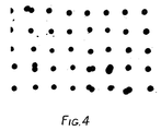
- A negative-acting "Toray Waterless Plate" 47.8 cm in length and 12 cm in width was developed to have a uniform pattern of roughly circular silicone rubber dots in rows extending longitudinally and transversely. The dots were uniformly about 60 µm in diameter on 0.29-mm centers. The developed plate was mounted on a cylinder with its length in the circumferential direction, leaving a seam of about 1 mm. Using apparatus as shown in Fig. 1, the cylinder was rotated in a fluidized bed of particles, each having a glass bead core about 60 µm in diameter and a silver surface layer about 0.5 µm thick. Particles carried by the Toray plate to the transfer roll were pressed into the adhesive layer of a transfer tape. Its adhesive was a phenyl-containing siloxane pressure-sensitive adhesive (GE 6574), 50 µm thick, and its backing was 60 µm biaxially oriented poly(ethyleneterephthalate) film, each surface of which had been provided with a low-adhesion backsize coating of a perfluoropolyether polymer as disclosed in U.S. Pat. No. 4,472,480. The resulting electrically conductive adhesive transfer tape was wound upon itself into a roll for storage. After being unwound, a photomicrograph was made of the face of the tape, a fragment of which is shown in Fig. 4 of the drawing. The full photomicrograph showed only one particle at almost every dot and two side-by-side particles at a few dots. A highlight at the top of each particle suggests that each particle is partially uncoated.
- Two electrically conductive pressure-sensitive adhesive tapes were made as in Example 2 except that the silicone rubber dots were about 100 µm in diameter. The dots were on 1.27-mm centers when making the tape of Example 3 and on 0.63-mm centers when making the tape of Example 4. Each of these tapes was tested for 180° peel adhesion in comparison to a "control" tape which was identical except having no particles. The 180° peel adhesion was measured from glass under ASTM D330-81, Method B, except using an "I-mass" adhesion tester 3M-90 in a controlled atmosphere of 22°C and 50% relative humidity. Initial adhesion measurements were made within five minutes after adhering a tape to the glass at 22°C. Some of the specimens were placed in an oven at 70°C for either 3 or 5 days and then held at the aforementioned controlled atmosphere overnight before testing. Results reported in Table I include testing of both the face side (FS) and the back side (BS). Also reported in Table I are tests for electrical resistance at 22°C, 50% RH, between two electrodes, each about 2.5 cm square, adhered to each other by one of these tapes.
TABLE I Tape of Example 180° Peel Adhesion (N/dm) Electrical Resistance (ohms/cm²) Initial After 3 days at 70°C After 5 days at 70°C FS BS FS BS FS BS 3 13.1 17.1 15.1 18.0 17.1 17.1 0.0071 4 13.7 17.4 12.6 14.8 15.4 15.7 0.0069 Control 17.5 17.4 15.9 15.9 15.9 16.5 10⁸ - Although the initial 180° peel adhesion of the face side (FS) of each of the tapes of Examples 3 and 4 somewhat lower than that of the control, the values are close enough to indicate that strong bonds can be made at ambient temperatures. The differences in 180° peel adhesion values of the tapes of Examples 3 and 4 versus the control tape are within experimental error. Hence, the electrically conductive particles are not interfering with adhesive values. The electrical conductivities of the tapes of Examples 3 and 4 are surprisingly good, considering the relatively wide spacing between their electrically conductive particles.
- An electrically conductive pressure-sensitive adhesive transfer tape was made as in Example 2 except that the particles were on 125-µm centers. Used to test the electrical conductivity of this tape was a rigid printed circuit board having a first set of 17 parallel solder-coated copper electrode strips, each 35 µm thick and 1.4 mm wide, spaced 1.1 mm from adjacent electrode strips, and a second identical set of 17 electrically conductive electrode strips aligned lengthwise with and spaced 2.5 cm from the first set. A strip of this adhesive transfer tape was used to adhere, to each of the two sets, one end of a 6-cm long flexible printed circuit (on polyimide film 25 µm thick) having a third identical set of electrically conductive strips, with one strip at each end of the flexible printed circuit overlying one set of 17 strips of the rigid printed circuit over a length of 1 cm. Good adhesive contact was assured by pressing with a hand-held wooden roller. The flexible printed circuit formed a loop rising above the rigid printed circuit, thus creating a modest lifting force that did not cause any adhesive failure.
- A load of 7 amperes at 12 volts DC was carried between aligned pairs of conductive strips of the first and second sets, but at 8 amperes the conductive strip of the flexible printed circuit failed in the manner of a wire fuse. The same result was obtained between other aligned conductors of the first and second sets. From this, it was determined that the adhesive transfer tape could carry at least 60 amperes/cm² DC through its thickness.
- An electrically conductive pressure-sensitive adhesive transfer tape was made as in Example 2 except that the silicone rubber dots were about 100 µm in diameter and on 0.625-mm centers. Every dot attracted at least one particle, and there were at least 2 particles, and occasionally 3, at about half of the dots.
- The resulting electrically conductive adhesive layer of the transfer tape was used to interconnect two sets of 17 electrode strips in the same manner as in Example 5.
- A power source was connected to each electrode of one set on the rigid printed circuit board, and a box containing 14 light emitting diodes (LEDs) was connected to 14 of the 17 electrode strips of the other set. The power source pulsed current sequentially through the 14 connected pairs so as to sequentially illuminate each of the 14 LEDs. This assembly was used for demonstration purposes for about three months, running some days for 6 or 7 hours. Every LED always lighted, and no more than one LED ever lighted at one time, thus indicating that there was no shorting caused by the strips of adhesive transfer tape.
Claims (10)
said particles have a Knoop Hardness Value of at least 300, so that when substrates comprising electrically conductive elements are adhered together with a piece of the tape, the particles penetrate those elements upon application of ordinary hand pressure.
Applications Claiming Priority (2)
| Application Number | Priority Date | Filing Date | Title |
|---|---|---|---|
| US16077388A | 1988-02-26 | 1988-02-26 | |
| US160773 | 1988-02-26 |
Publications (3)
| Publication Number | Publication Date |
|---|---|
| EP0330452A2 true EP0330452A2 (en) | 1989-08-30 |
| EP0330452A3 EP0330452A3 (en) | 1991-12-27 |
| EP0330452B1 EP0330452B1 (en) | 1994-04-27 |
Family
ID=22578381
Family Applications (1)
| Application Number | Title | Priority Date | Filing Date |
|---|---|---|---|
| EP89301733A Expired - Lifetime EP0330452B1 (en) | 1988-02-26 | 1989-02-22 | Electrically conductive pressure-sensitive adhesive tape |
Country Status (9)
| Country | Link |
|---|---|
| US (2) | US5300340A (en) |
| EP (1) | EP0330452B1 (en) |
| JP (1) | JPH02160311A (en) |
| KR (1) | KR970008547B1 (en) |
| AU (1) | AU612771B2 (en) |
| BR (1) | BR8900822A (en) |
| CA (1) | CA1317002C (en) |
| DE (1) | DE68914867T2 (en) |
| ES (1) | ES2053975T3 (en) |
Cited By (24)
| Publication number | Priority date | Publication date | Assignee | Title |
|---|---|---|---|---|
| EP0422919A2 (en) * | 1989-10-11 | 1991-04-17 | WATERFORD RESEARCH & DEVELOPMENT LIMITED | Antistatic adhesive tape |
| US5087494A (en) * | 1991-04-12 | 1992-02-11 | Minnesota Mining And Manufacturing Company | Electrically conductive adhesive tape |
| US5141790A (en) * | 1989-11-20 | 1992-08-25 | Minnesota Mining And Manufacturing Company | Repositionable pressure-sensitive adhesive tape |
| EP0508722A1 (en) * | 1991-04-12 | 1992-10-14 | Minnesota Mining And Manufacturing Company | Electrically conductive adhesive tape |
| US5273805A (en) * | 1991-08-05 | 1993-12-28 | Minnesota Mining And Manufacturing Company | Structured flexible carrier web with recess areas bearing a layer of silicone on predetermined surfaces |
| US5308667A (en) * | 1992-10-16 | 1994-05-03 | Minnesota Mining And Manufacturing Company | Electrically conductive adhesive web |
| WO1995004387A1 (en) * | 1993-07-27 | 1995-02-09 | Citizen Watch Co., Ltd. | An electrical connecting structure and a method for electrically connecting terminals to each other |
| EP0691660A1 (en) * | 1994-05-10 | 1996-01-10 | Hitachi Chemical Co., Ltd. | Anisotropically electroconductive resin film |
| WO1997025844A1 (en) * | 1996-01-05 | 1997-07-17 | Alliedsignal Inc. | Printed circuit multilayer assembly and method of manufacture therefor |
| US5769996A (en) * | 1994-01-27 | 1998-06-23 | Loctite (Ireland) Limited | Compositions and methods for providing anisotropic conductive pathways and bonds between two sets of conductors |
| US5851644A (en) * | 1995-08-01 | 1998-12-22 | Loctite (Ireland) Limited | Films and coatings having anisotropic conductive pathways therein |
| US5916641A (en) * | 1996-08-01 | 1999-06-29 | Loctite (Ireland) Limited | Method of forming a monolayer of particles |
| WO2000000563A1 (en) * | 1998-06-30 | 2000-01-06 | Minnesota Mining And Manufacturing Company | Fine pitch anisotropic conductive adhesive |
| US6147870A (en) * | 1996-01-05 | 2000-11-14 | Honeywell International Inc. | Printed circuit assembly having locally enhanced wiring density |
| US6180226B1 (en) | 1996-08-01 | 2001-01-30 | Loctite (R&D) Limited | Method of forming a monolayer of particles, and products formed thereby |
| US6402876B1 (en) | 1997-08-01 | 2002-06-11 | Loctite (R&D) Ireland | Method of forming a monolayer of particles, and products formed thereby |
| US6977025B2 (en) | 1996-08-01 | 2005-12-20 | Loctite (R&D) Limited | Method of forming a monolayer of particles having at least two different sizes, and products formed thereby |
| DE102011075009A1 (en) * | 2011-04-29 | 2012-10-31 | Continental Automotive Gmbh | On a carrier arranged contact surface for connection to a arranged on another carrier mating contact surface and device having a contact surface and a mating contact surface connected thereto |
| AT511655B1 (en) * | 2011-10-20 | 2013-02-15 | Prelonic Technologies Gmbh | METHOD FOR BONDING CIRCUIT ELEMENTS AND ADHESIVES |
| EP2640173A2 (en) * | 2006-05-03 | 2013-09-18 | Trillion Science, Inc. | Method for fabricating an electronic device |
| US9102851B2 (en) | 2011-09-15 | 2015-08-11 | Trillion Science, Inc. | Microcavity carrier belt and method of manufacture |
| GB2572649A (en) * | 2018-04-06 | 2019-10-09 | Illinois Tool Works | Improved adhesive roll |
| WO2021008190A1 (en) * | 2019-07-17 | 2021-01-21 | 苏州微邦材料科技有限公司 | Pressure-sensitive conductive adhesive tape and application thereof in photovoltaic cell sheet lamination |
| WO2021124038A1 (en) * | 2019-12-17 | 2021-06-24 | 3M Innovative Properties Company | Transfer tape articles for preparing dry electrodes |
Families Citing this family (49)
| Publication number | Priority date | Publication date | Assignee | Title |
|---|---|---|---|---|
| US5366140A (en) * | 1993-09-30 | 1994-11-22 | Minnesota Mining And Manufacturing Company | Patterned array of uniform metal microbeads |
| US6440880B2 (en) * | 1993-10-29 | 2002-08-27 | 3M Innovative Properties Company | Pressure-sensitive adhesives having microstructured surfaces |
| US5527591A (en) * | 1994-12-02 | 1996-06-18 | Augat Inc. | Electrical contact having a particulate surface |
| US5685939A (en) * | 1995-03-10 | 1997-11-11 | Minnesota Mining And Manufacturing Company | Process for making a Z-axis adhesive and establishing electrical interconnection therewith |
| US5801446A (en) * | 1995-03-28 | 1998-09-01 | Tessera, Inc. | Microelectronic connections with solid core joining units |
| US5795636A (en) * | 1995-11-15 | 1998-08-18 | Minnesota Mining And Manufacturing Company | Positionable and repositionable adhesive article |
| DE19642178A1 (en) * | 1996-10-12 | 1998-04-16 | Beiersdorf Ag | Electrically conductive transfer tape |
| US5897930A (en) * | 1996-12-31 | 1999-04-27 | Minnesota Mining And Manufacturing Company | Multiple embossed webs |
| US6197397B1 (en) * | 1996-12-31 | 2001-03-06 | 3M Innovative Properties Company | Adhesives having a microreplicated topography and methods of making and using same |
| JP3097619B2 (en) * | 1997-10-02 | 2000-10-10 | 日本電気株式会社 | Method of manufacturing field emission cold cathode |
| US6217981B1 (en) * | 1997-10-13 | 2001-04-17 | 3M Innovative Properties Company | Adhesive sheet and method for producing the same |
| US6096982A (en) * | 1998-02-18 | 2000-08-01 | Nanopierce Technologies, Inc. | Method and apparatus for conductively joining components |
| GB9808221D0 (en) * | 1998-04-17 | 1998-06-17 | Sharp Kk | Liquid crystal device manufacturing methods |
| DE19853805B4 (en) | 1998-11-21 | 2005-05-12 | Tesa Ag | Electrically conductive, thermoplastic and heat-activatable adhesive film and their use |
| US6524675B1 (en) * | 1999-05-13 | 2003-02-25 | 3M Innovative Properties Company | Adhesive-back articles |
| US20020119255A1 (en) | 2000-05-09 | 2002-08-29 | Ranjith Divigalpitiya | Method and apparatus for making particle-embedded webs |
| US6569494B1 (en) * | 2000-05-09 | 2003-05-27 | 3M Innovative Properties Company | Method and apparatus for making particle-embedded webs |
| US20040087128A1 (en) * | 2000-10-24 | 2004-05-06 | Neuhaus Herbert J | Method and materials for printing particle-enhanced electrical contacts |
| CA2350853A1 (en) * | 2001-06-15 | 2002-12-15 | Groupe Minutia Inc. | Method of establishing electrical conductivity between oxide-coated electrical conductors |
| US6926725B2 (en) * | 2002-04-04 | 2005-08-09 | Rex Medical, L.P. | Thrombectomy device with multi-layered rotational wire |
| DE10259549A1 (en) * | 2002-12-19 | 2004-07-08 | Tesa Ag | PSA article with at least one layer of an electrically conductive PSA and process for its production |
| US7034403B2 (en) * | 2003-04-10 | 2006-04-25 | 3M Innovative Properties Company | Durable electronic assembly with conductive adhesive |
| US7309837B1 (en) * | 2003-09-17 | 2007-12-18 | Rauckman James B | Wildlife guard for electrical power distribution and substation facilities |
| DE102004031189A1 (en) * | 2004-06-28 | 2006-01-19 | Tesa Ag | Heat-activated and crosslinkable adhesive tape for the bonding of electronic components and printed conductors |
| KR20060018453A (en) * | 2004-08-24 | 2006-03-02 | 삼성전자주식회사 | Semiconductor device comprising heat sink |
| FR2880540B1 (en) * | 2005-01-13 | 2008-07-11 | Aventis Pharma Sa | USE OF PURINE DERIVATIVES AS INHIBITORS OF HSP90 PROTEIN |
| US8802214B2 (en) * | 2005-06-13 | 2014-08-12 | Trillion Science, Inc. | Non-random array anisotropic conductive film (ACF) and manufacturing processes |
| US7773337B2 (en) * | 2006-02-10 | 2010-08-10 | Seagate Technology Llc | Tamper evident tape with integrated EMI shielding |
| JP2007299907A (en) * | 2006-04-28 | 2007-11-15 | Nitto Denko Corp | Structure having property of conducting or absorbing electromagnetic wave |
| US7923488B2 (en) * | 2006-10-16 | 2011-04-12 | Trillion Science, Inc. | Epoxy compositions |
| US20110214735A1 (en) * | 2008-11-07 | 2011-09-08 | 3M Innovative Properities Company | Conductive laminated assembly |
| US9061478B2 (en) | 2011-05-18 | 2015-06-23 | 3M Innovative Properties Company | Conductive nonwoven pressure sensitive adhesive tapes and articles therefrom |
| DE102011080729A1 (en) | 2011-08-10 | 2013-02-14 | Tesa Se | Electrically conductive pressure-sensitive adhesive and pressure-sensitive adhesive tape |
| DE102011080724A1 (en) | 2011-08-10 | 2013-02-14 | Tesa Se | Electrically conductive heat-activatable adhesive |
| US9475963B2 (en) | 2011-09-15 | 2016-10-25 | Trillion Science, Inc. | Fixed array ACFs with multi-tier partially embedded particle morphology and their manufacturing processes |
| US9426878B2 (en) | 2011-10-25 | 2016-08-23 | 3M Innovative Properties Company | Nonwoven adhesive tapes and articles therefrom |
| DE102012207462A1 (en) | 2012-05-04 | 2013-11-07 | Tesa Se | Three-dimensional electrically conductive adhesive film |
| US9352539B2 (en) * | 2013-03-12 | 2016-05-31 | Trillion Science, Inc. | Microcavity carrier with image enhancement for laser ablation |
| GB2521678A (en) * | 2013-12-31 | 2015-07-01 | Intelligent Energy Ltd | Fuel cell flow plate |
| EP3122248A4 (en) * | 2014-03-28 | 2018-05-02 | Board of Regents, The University of Texas System | Epidermal sensor system and process |
| US10492703B2 (en) | 2014-03-28 | 2019-12-03 | Board Of Regents, The University Of Texas System | Epidermal sensor system and process |
| JP6682804B2 (en) * | 2014-10-28 | 2020-04-15 | デクセリアルズ株式会社 | Anisotropic conductive film |
| KR101956221B1 (en) * | 2014-10-28 | 2019-03-08 | 데쿠세리아루즈 가부시키가이샤 | Anisotropic conductive film, manufacturing method for same, and connection structure |
| JP6682805B2 (en) * | 2014-10-28 | 2020-04-15 | デクセリアルズ株式会社 | Anisotropic conductive film |
| US9595501B1 (en) * | 2015-10-30 | 2017-03-14 | Automated Assembly Corporation | Wire bonded electronic devices to round wire |
| EP3436259A4 (en) * | 2016-03-30 | 2020-02-05 | 3M Innovative Properties Company | Article featuring a predetermined pattern of randomly distributed microspheres and methods of making the same |
| WO2017191772A1 (en) | 2016-05-05 | 2017-11-09 | デクセリアルズ株式会社 | Filler alignment film |
| JP7119288B2 (en) * | 2016-05-05 | 2022-08-17 | デクセリアルズ株式会社 | filler placement film |
| US10058014B1 (en) | 2017-12-13 | 2018-08-21 | International Business Machines Corporation | Conductive adhesive layer for gasket assembly |
Citations (2)
| Publication number | Priority date | Publication date | Assignee | Title |
|---|---|---|---|---|
| US4606962A (en) * | 1983-06-13 | 1986-08-19 | Minnesota Mining And Manufacturing Company | Electrically and thermally conductive adhesive transfer tape |
| DE8708027U1 (en) * | 1987-06-05 | 1987-09-10 | Preh, Elektrofeinmechanische Werke Jakob Preh Nachf. Gmbh & Co, 8740 Bad Neustadt, De |
Family Cites Families (15)
| Publication number | Priority date | Publication date | Assignee | Title |
|---|---|---|---|---|
| US3475213A (en) * | 1965-09-13 | 1969-10-28 | Minnesota Mining & Mfg | Electrically conductive adhesive tape |
| US3511178A (en) * | 1967-01-06 | 1970-05-12 | Minnesota Mining & Mfg | Printing plate and method |
| US3514326A (en) * | 1967-11-17 | 1970-05-26 | Minnesota Mining & Mfg | Tape |
| US4113981A (en) * | 1974-08-14 | 1978-09-12 | Kabushiki Kaisha Seikosha | Electrically conductive adhesive connecting arrays of conductors |
| US4054714A (en) * | 1976-06-07 | 1977-10-18 | E. I. Du Pont De Nemours And Company | Electrically conductive adhesive composition |
| JPS5724456Y2 (en) * | 1977-09-09 | 1982-05-27 | ||
| US4447492A (en) * | 1977-11-21 | 1984-05-08 | Occidental Chemical Corporation | Articles having an electrically conductive surface |
| US4247594A (en) * | 1979-04-30 | 1981-01-27 | Marshall & Pike Enterprises Inc. | Electrically conductive resinous composition |
| US4472480A (en) * | 1982-07-02 | 1984-09-18 | Minnesota Mining And Manufacturing Company | Low surface energy liner of perfluoropolyether |
| US4568602A (en) * | 1983-01-24 | 1986-02-04 | Minnesota Mining And Manufacturing Company | Sheet material adapted to provide long-lived stable adhesive-bonded electrical connections |
| US4546037A (en) * | 1984-09-04 | 1985-10-08 | Minnesota Mining And Manufacturing Company | Flexible tape having stripes of electrically conductive particles for making multiple connections |
| US4548862A (en) * | 1984-09-04 | 1985-10-22 | Minnesota Mining And Manufacturing Company | Flexible tape having bridges of electrically conductive particles extending across its pressure-sensitive adhesive layer |
| US4737112A (en) * | 1986-09-05 | 1988-04-12 | American Telephone And Telegraph Company, At&T Bell Laboratories | Anisotropically conductive composite medium |
| JPS63249393A (en) * | 1987-04-03 | 1988-10-17 | シャープ株式会社 | Method of connecting electronic component |
| US5225966A (en) * | 1991-07-24 | 1993-07-06 | At&T Bell Laboratories | Conductive adhesive film techniques |
-
1989
- 1989-01-20 AU AU28661/89A patent/AU612771B2/en not_active Ceased
- 1989-01-23 CA CA000588885A patent/CA1317002C/en not_active Expired - Fee Related
- 1989-02-22 DE DE68914867T patent/DE68914867T2/en not_active Expired - Fee Related
- 1989-02-22 ES ES89301733T patent/ES2053975T3/en not_active Expired - Lifetime
- 1989-02-22 EP EP89301733A patent/EP0330452B1/en not_active Expired - Lifetime
- 1989-02-23 JP JP1045006A patent/JPH02160311A/en active Pending
- 1989-02-23 BR BR898900822A patent/BR8900822A/en not_active IP Right Cessation
- 1989-02-24 KR KR1019890002193A patent/KR970008547B1/en not_active IP Right Cessation
-
1992
- 1992-04-22 US US07/874,553 patent/US5300340A/en not_active Expired - Lifetime
-
1994
- 1994-02-08 US US08/193,297 patent/US5494730A/en not_active Expired - Lifetime
Patent Citations (2)
| Publication number | Priority date | Publication date | Assignee | Title |
|---|---|---|---|---|
| US4606962A (en) * | 1983-06-13 | 1986-08-19 | Minnesota Mining And Manufacturing Company | Electrically and thermally conductive adhesive transfer tape |
| DE8708027U1 (en) * | 1987-06-05 | 1987-09-10 | Preh, Elektrofeinmechanische Werke Jakob Preh Nachf. Gmbh & Co, 8740 Bad Neustadt, De |
Cited By (37)
| Publication number | Priority date | Publication date | Assignee | Title |
|---|---|---|---|---|
| EP0422919A3 (en) * | 1989-10-11 | 1992-05-27 | Waterford Research & Development Limited | Antistatic adhesive tape |
| EP0422919A2 (en) * | 1989-10-11 | 1991-04-17 | WATERFORD RESEARCH & DEVELOPMENT LIMITED | Antistatic adhesive tape |
| US5141790A (en) * | 1989-11-20 | 1992-08-25 | Minnesota Mining And Manufacturing Company | Repositionable pressure-sensitive adhesive tape |
| EP0508722A1 (en) * | 1991-04-12 | 1992-10-14 | Minnesota Mining And Manufacturing Company | Electrically conductive adhesive tape |
| US5087494A (en) * | 1991-04-12 | 1992-02-11 | Minnesota Mining And Manufacturing Company | Electrically conductive adhesive tape |
| US5273805A (en) * | 1991-08-05 | 1993-12-28 | Minnesota Mining And Manufacturing Company | Structured flexible carrier web with recess areas bearing a layer of silicone on predetermined surfaces |
| US5462765A (en) * | 1991-08-05 | 1995-10-31 | Minnesota Mining And Manufacturing Company | Structured flexible carrier web bearing a layer of silicone on predetermined surfaces |
| US5308667A (en) * | 1992-10-16 | 1994-05-03 | Minnesota Mining And Manufacturing Company | Electrically conductive adhesive web |
| US6101708A (en) * | 1993-07-27 | 2000-08-15 | Citizen Watch Co., Ltd. | Method for electrically connecting terminals to each other |
| WO1995004387A1 (en) * | 1993-07-27 | 1995-02-09 | Citizen Watch Co., Ltd. | An electrical connecting structure and a method for electrically connecting terminals to each other |
| US5679928A (en) * | 1993-07-27 | 1997-10-21 | Citizen Watch Co., Ltd. | Electrical connecting structure for electrically connecting terminals to each other |
| US6110399A (en) * | 1994-01-27 | 2000-08-29 | Loctite (Ireland) Limited | Compositions and method for providing anisotropic conductive pathways and bonds between two sets of conductors |
| US5769996A (en) * | 1994-01-27 | 1998-06-23 | Loctite (Ireland) Limited | Compositions and methods for providing anisotropic conductive pathways and bonds between two sets of conductors |
| EP0691660A1 (en) * | 1994-05-10 | 1996-01-10 | Hitachi Chemical Co., Ltd. | Anisotropically electroconductive resin film |
| US6042894A (en) * | 1994-05-10 | 2000-03-28 | Hitachi Chemical Company, Ltd. | Anisotropically electroconductive resin film |
| US5851644A (en) * | 1995-08-01 | 1998-12-22 | Loctite (Ireland) Limited | Films and coatings having anisotropic conductive pathways therein |
| US6149857A (en) * | 1995-08-01 | 2000-11-21 | Loctite (R&D) Limited | Method of making films and coatings having anisotropic conductive pathways therein |
| US5839188A (en) * | 1996-01-05 | 1998-11-24 | Alliedsignal Inc. | Method of manufacturing a printed circuit assembly |
| WO1997025844A1 (en) * | 1996-01-05 | 1997-07-17 | Alliedsignal Inc. | Printed circuit multilayer assembly and method of manufacture therefor |
| US6147870A (en) * | 1996-01-05 | 2000-11-14 | Honeywell International Inc. | Printed circuit assembly having locally enhanced wiring density |
| US6246014B1 (en) | 1996-01-05 | 2001-06-12 | Honeywell International Inc. | Printed circuit assembly and method of manufacture therefor |
| US5916641A (en) * | 1996-08-01 | 1999-06-29 | Loctite (Ireland) Limited | Method of forming a monolayer of particles |
| US6977025B2 (en) | 1996-08-01 | 2005-12-20 | Loctite (R&D) Limited | Method of forming a monolayer of particles having at least two different sizes, and products formed thereby |
| US6180226B1 (en) | 1996-08-01 | 2001-01-30 | Loctite (R&D) Limited | Method of forming a monolayer of particles, and products formed thereby |
| US6402876B1 (en) | 1997-08-01 | 2002-06-11 | Loctite (R&D) Ireland | Method of forming a monolayer of particles, and products formed thereby |
| WO2000000563A1 (en) * | 1998-06-30 | 2000-01-06 | Minnesota Mining And Manufacturing Company | Fine pitch anisotropic conductive adhesive |
| EP2640173A2 (en) * | 2006-05-03 | 2013-09-18 | Trillion Science, Inc. | Method for fabricating an electronic device |
| EP2640173A3 (en) * | 2006-05-03 | 2014-10-01 | Trillion Science, Inc. | Method for fabricating an electronic device |
| DE102011075009A1 (en) * | 2011-04-29 | 2012-10-31 | Continental Automotive Gmbh | On a carrier arranged contact surface for connection to a arranged on another carrier mating contact surface and device having a contact surface and a mating contact surface connected thereto |
| US9332640B2 (en) | 2011-04-29 | 2016-05-03 | Continental Automotive Gmbh | Contact surface arranged on a carrier for connecting to a counter contact surface arranged on a further carrier, and device comprising a contact surface and a counter contact surface connected thereto |
| DE102011075009B4 (en) * | 2011-04-29 | 2019-11-14 | Continental Automotive Gmbh | On a support arranged contact surface for connection to a arranged on a further carrier mating contact surface |
| US9102851B2 (en) | 2011-09-15 | 2015-08-11 | Trillion Science, Inc. | Microcavity carrier belt and method of manufacture |
| AT511655B1 (en) * | 2011-10-20 | 2013-02-15 | Prelonic Technologies Gmbh | METHOD FOR BONDING CIRCUIT ELEMENTS AND ADHESIVES |
| GB2572649A (en) * | 2018-04-06 | 2019-10-09 | Illinois Tool Works | Improved adhesive roll |
| WO2019195011A1 (en) * | 2018-04-06 | 2019-10-10 | Illinois Tool Works Inc. | Improved adhesive roll |
| WO2021008190A1 (en) * | 2019-07-17 | 2021-01-21 | 苏州微邦材料科技有限公司 | Pressure-sensitive conductive adhesive tape and application thereof in photovoltaic cell sheet lamination |
| WO2021124038A1 (en) * | 2019-12-17 | 2021-06-24 | 3M Innovative Properties Company | Transfer tape articles for preparing dry electrodes |
Also Published As
| Publication number | Publication date |
|---|---|
| DE68914867T2 (en) | 1994-11-10 |
| US5300340A (en) | 1994-04-05 |
| JPH02160311A (en) | 1990-06-20 |
| AU612771B2 (en) | 1991-07-18 |
| US5494730A (en) | 1996-02-27 |
| CA1317002C (en) | 1993-04-27 |
| KR970008547B1 (en) | 1997-05-27 |
| ES2053975T3 (en) | 1994-08-01 |
| EP0330452B1 (en) | 1994-04-27 |
| EP0330452A3 (en) | 1991-12-27 |
| DE68914867D1 (en) | 1994-06-01 |
| KR890013673A (en) | 1989-09-25 |
| AU2866189A (en) | 1989-08-31 |
| BR8900822A (en) | 1989-10-17 |
Similar Documents
| Publication | Publication Date | Title |
|---|---|---|
| EP0330452B1 (en) | Electrically conductive pressure-sensitive adhesive tape | |
| US5240761A (en) | Electrically conductive adhesive tape | |
| EP0613590B1 (en) | Die mounting with uniaxial conductive adhesive | |
| EP1093503B1 (en) | Fine pitch anisotropic conductive adhesive | |
| US6841022B2 (en) | Adhesive-coated electronic parts on a connection sheet | |
| US5087494A (en) | Electrically conductive adhesive tape | |
| EP1132961B1 (en) | Method for producing a circuit substrate having a mounted semiconductor element | |
| JPH05198709A (en) | Thermal-conductive boundary surface material and usage thereof | |
| CA1247943A (en) | Electrically and thermally conductive adhesive transfer tape | |
| EP0508722A1 (en) | Electrically conductive adhesive tape | |
| JP3959654B2 (en) | Multi-chip mounting method | |
| JP4147614B2 (en) | Rolled body having an adhesive layer | |
| JP2001052780A (en) | Electric connector and its manufacture | |
| CA1234887A (en) | Multiple-connector adhesive tape | |
| KR100251674B1 (en) | Connection sheet for interconnecting electrodes facing each other, and electrode connection structure and method using the connection sheet | |
| US20030019735A1 (en) | Bonding electrical components to substrates | |
| JP4223581B2 (en) | Multi-chip mounting method | |
| JP4045471B2 (en) | Electronic component mounting method | |
| EP0308980A2 (en) | Flat wire in silicone rubber or matrix MOE | |
| JPH10125433A (en) | Low-resistance connector and manufacture thereof | |
| JPH0429444Y2 (en) | ||
| JPH11121073A (en) | Connecting member and its manufacture | |
| JPS6055958B2 (en) | Conductive part connection wiring method and connection wiring materials |
Legal Events
| Date | Code | Title | Description |
|---|---|---|---|
| PUAI | Public reference made under article 153(3) epc to a published international application that has entered the european phase |
Free format text: ORIGINAL CODE: 0009012 |
|
| AK | Designated contracting states |
Kind code of ref document: A2 Designated state(s): DE ES FR GB IT SE |
|
| 17P | Request for examination filed |
Effective date: 19910102 |
|
| PUAL | Search report despatched |
Free format text: ORIGINAL CODE: 0009013 |
|
| AK | Designated contracting states |
Kind code of ref document: A3 Designated state(s): DE ES FR GB IT SE |
|
| 17Q | First examination report despatched |
Effective date: 19920810 |
|
| GRAA | (expected) grant |
Free format text: ORIGINAL CODE: 0009210 |
|
| AK | Designated contracting states |
Kind code of ref document: B1 Designated state(s): DE ES FR GB IT SE |
|
| REF | Corresponds to: |
Ref document number: 68914867 Country of ref document: DE Date of ref document: 19940601 |
|
| ITF | It: translation for a ep patent filed |
Owner name: ING. C. GREGORJ S.P.A. |
|
| REG | Reference to a national code |
Ref country code: ES Ref legal event code: FG2A Ref document number: 2053975 Country of ref document: ES Kind code of ref document: T3 |
|
| ET | Fr: translation filed | ||
| EAL | Se: european patent in force in sweden |
Ref document number: 89301733.5 |
|
| PLBE | No opposition filed within time limit |
Free format text: ORIGINAL CODE: 0009261 |
|
| STAA | Information on the status of an ep patent application or granted ep patent |
Free format text: STATUS: NO OPPOSITION FILED WITHIN TIME LIMIT |
|
| 26N | No opposition filed | ||
| PGFP | Annual fee paid to national office [announced via postgrant information from national office to epo] |
Ref country code: SE Payment date: 19980120 Year of fee payment: 10 |
|
| PGFP | Annual fee paid to national office [announced via postgrant information from national office to epo] |
Ref country code: FR Payment date: 19980121 Year of fee payment: 10 |
|
| PGFP | Annual fee paid to national office [announced via postgrant information from national office to epo] |
Ref country code: DE Payment date: 19980123 Year of fee payment: 10 |
|
| PGFP | Annual fee paid to national office [announced via postgrant information from national office to epo] |
Ref country code: GB Payment date: 19980127 Year of fee payment: 10 |
|
| PGFP | Annual fee paid to national office [announced via postgrant information from national office to epo] |
Ref country code: ES Payment date: 19980216 Year of fee payment: 10 |
|
| PG25 | Lapsed in a contracting state [announced via postgrant information from national office to epo] |
Ref country code: GB Free format text: LAPSE BECAUSE OF NON-PAYMENT OF DUE FEES Effective date: 19990222 |
|
| PG25 | Lapsed in a contracting state [announced via postgrant information from national office to epo] |
Ref country code: SE Free format text: LAPSE BECAUSE OF NON-PAYMENT OF DUE FEES Effective date: 19990223 Ref country code: ES Free format text: LAPSE BECAUSE OF NON-PAYMENT OF DUE FEES Effective date: 19990223 |
|
| GBPC | Gb: european patent ceased through non-payment of renewal fee |
Effective date: 19990222 |
|
| PG25 | Lapsed in a contracting state [announced via postgrant information from national office to epo] |
Ref country code: FR Free format text: LAPSE BECAUSE OF NON-PAYMENT OF DUE FEES Effective date: 19991029 |
|
| EUG | Se: european patent has lapsed |
Ref document number: 89301733.5 |
|
| PG25 | Lapsed in a contracting state [announced via postgrant information from national office to epo] |
Ref country code: DE Free format text: LAPSE BECAUSE OF NON-PAYMENT OF DUE FEES Effective date: 19991201 |
|
| REG | Reference to a national code |
Ref country code: FR Ref legal event code: ST |
|
| REG | Reference to a national code |
Ref country code: ES Ref legal event code: FD2A Effective date: 20010910 |
|
| PG25 | Lapsed in a contracting state [announced via postgrant information from national office to epo] |
Ref country code: IT Free format text: LAPSE BECAUSE OF NON-PAYMENT OF DUE FEES;WARNING: LAPSES OF ITALIAN PATENTS WITH EFFECTIVE DATE BEFORE 2007 MAY HAVE OCCURRED AT ANY TIME BEFORE 2007. THE CORRECT EFFECTIVE DATE MAY BE DIFFERENT FROM THE ONE RECORDED. Effective date: 20050222 |