EP0330087A2 - Extended storage system - Google Patents
Extended storage system Download PDFInfo
- Publication number
- EP0330087A2 EP0330087A2 EP89102752A EP89102752A EP0330087A2 EP 0330087 A2 EP0330087 A2 EP 0330087A2 EP 89102752 A EP89102752 A EP 89102752A EP 89102752 A EP89102752 A EP 89102752A EP 0330087 A2 EP0330087 A2 EP 0330087A2
- Authority
- EP
- European Patent Office
- Prior art keywords
- storage
- data
- buffer
- transfer
- extended
- Prior art date
- Legal status (The legal status is an assumption and is not a legal conclusion. Google has not performed a legal analysis and makes no representation as to the accuracy of the status listed.)
- Granted
Links
Images


Classifications
-
- G—PHYSICS
- G06—COMPUTING; CALCULATING OR COUNTING
- G06F—ELECTRIC DIGITAL DATA PROCESSING
- G06F12/00—Accessing, addressing or allocating within memory systems or architectures
- G06F12/02—Addressing or allocation; Relocation
- G06F12/08—Addressing or allocation; Relocation in hierarchically structured memory systems, e.g. virtual memory systems
Definitions
- This invention relates to an extended storage system for a data processing system, and particularly to an extended storage system suited to transfer data between hierarchical storages and an extended storage.
- U.S. Patent No. 4,476,524 issued to D.T. Braun et al. on October 9, 1984 discloses a data processing system which includes a data transfer path between a main storage (will be termed MS hereinafter) and an extended storage (or page storage) and performs data transfer between the MS and extended storage using the data transfer path.
- MS main storage
- extended storage or page storage
- JP-A-52-71138 dicloses hierarchical storages in which a small-capacity, high-speed high ranking storage, e.g., a buffer storage (will be termed BS hereinafter) is provided on the part of the processor, and an intermediate-rank storage, e.g., a work storage (will be termed WS hereinafter) serving as a second-rank buffer, having an intermediate speed and intermediate capacity as compared with the BS and MS is provided between the BS and MS. In this case, the MS in the lowest-rank storage.
- a buffer storage will be termed BS hereinafter
- WS work storage
- the data In reading out data such as an instructions or operand stored in three or more hierarchical storages, the data is read out from a storage of as high rank as possible which holds the object data or contains a copy of the data. Only if any storage higher in rank than MS does not contain a copy of data, it is read out from the MS. Control is made to memorize data of much usage at a higher rank storage. The processing speed is thus enhanced.
- central processors CPs
- channel processors CHs
- SC system controller
- MSs main storages
- PSs page storages
- An object of this invention is to provide an extended storage system used suitably for transferring data between hierarchical storages of three ranks or more and an extended storage.
- Another object of this invention is to provide an extended storage system which ensures the latest version of copied data by merely having means which, following a data transfer from an extended storage to hierarchical storages, invalidates the copy of transfer destination data among data copied in a storage higher in rank than at least one intermediate-rank storage.
- a further object of this invention is to prevent improper data transfer to the ES from the MS whose contents would not be yet updated to the latest version due to the presence of an intermediate-rank work storage which is controlled in store-in mode and is higher in rank than the MS.
- a further object of this invention is to solve such a problem that, in case of data transfer from the ES to MS and in case that WS or BS higher in rank than the MS has a copy of data that has been stored in the MS until the transfer, the copied data in the WS or BS is inconsistent with the newly transferred data to the MS and the transferred data solely becomes new data.
- the above objectives are achieved through the provision, between at least one intermediate-rank storage controlled in store-in mode and an ES, of a data transfer path for the data transfer between the intermediate-rank storage and the ES, and means of invalidating transfer destination data of the data to be transferred in the hierarchical storages, i.e., portion corresponding to the data to be cancelled because of change in destinated portion, among data copied in a storage higher in rank than the intermediate-rank storage, and there can be achieved a data transfer from the ES to a hierarchical storage made similarly as the data transfer from a processor to the hierarchical storage.
- control means which, following a data transfer between the hierarchical storages and ES, invalidates or retards the transferred data in the intermediate-rank storage and storages excluding MS lower in rank than the intermediate-rank storage (intermediate/lower ranking storages). More specifically, if the WS has a copy of data to be cancelled which is already in the MS destination attributable to the transfer from ES to MS, it is cancelled. If the WS does not have a copy of data of MS destination to be cancelled, which case is not a normal store-in operation, an operation to copy the data into the WS is retarded, namely it is not made valid. The discrimination between "valid” and "invalid” can be made using flag means.
- the intermediate-rank storage when data is transferred from the MS or WS among hierarchical storages to the ES, the intermediate-rank storage is first referenced and, if the WS has a copy of the data to be transferred, the data is read out of the intermediate-rank storage and transferred to the ES, or, if the WS does not have the copy, the data is read out of the MS and transferred to the ES. Since storages higher in rank than the intermediate storage or BS are controlled in store-through mode, the transfer data read out as described above is always in the latest version among the WS and the BS.
- each storage within the intermediate-rank storage which has been referenced at reading of the transfer data invalidates the copy after the data has been read out, or, if the copy is absent, retards the copy in the self storage of the data read out from a lower-rank storage.
- the control means when data transfer takes place between hierarchical storages and ES, the intermediate-rank storage can be placed in a state of having no copy of the transfer data, and accordingly for a data transfer of less urgency the control means is activated so that the intermediate storage can be used more efficiently.
- the transfer is accompanied by copying by holding the generation of the command which activates the control means.
- the inventive extended storage system comprising hierarchical storages including, from higher to lower ranks, a buffer storage (BS) 3, a work storage (WS) 4 and a main storage (MS) 5, and an extended storage (ES) 6, with a data transfer path 70 being provided between the WS 4 and ES 6.
- the BS 3 and WS 4 are controlled in store-through mode and store-in mode, respectively.
- An instruction processor (IP) 1 and input/output processor (IOP) 2 dictate and control the data transfer between the WS 4 and ES 6 using an IP control signal line 80 and IOP control signal line 81, respectively.
- the ES 6 comprises an extended storage device (will be termed ESD) 65 which stores data from the WS 4, a transfer controller 61 which controls the transfer commands from the IP 1 and IOP 2, requesters 62 and 63 which issue write requests and read requests to the WS 4 and ESD 65, and a data buffer 64 which temporarily holds data from the WS 4 and ESD 65.
- ESD extended storage device
- the transfer controller 61 comprises, as shown in Fig. 3, transfer command registers 611 and 612 which hold and control the transfer commands from the IP 1 and IOP 2, a selector 613 which selects the output of the transfer command register 611 or 12, and a transfer controller 614 which generally controls data transfer.
- the transfer command register 611 comprise, as shown in Fig. 4, a command register 6111, a transfer volume register 6112, an MS address register 6113, an ES address register 6114, a subtracter 6115, adders 6116 and 6117, and a transfer end tester 6118 which detects that the transfer volume register 6112 becomes "empty".
- the transfer command register 612 has the same arrangement as 611.
- Commands of data transfer between WS 4 and ES 6 are sent to the ES 6 over the transfer command lines 801 and 811, respectively, depending on the operand of each command and the contents of a general-purpose register specified by command for a command from the IP 1, or depending on the channel command word (CCW) for a command from the IOP 2.
- the command contains the transfer direction between the WS 4 and ES 6, the specification of activation for the control means of copy invalidation/retardation to the WS 4, the MS address and ES address indicative of the starting addresses of the transfer source and transfer destination.
- Commands sent from the IP 1 are set in the respective registers 6111-6114 in the transfer command register 611, while command sent from the IOP 2 are set in the respective registers in the transfer command register 612.
- a command set in the transfer command register 611 or 612 is delivered to the transfer controller 614 over command line 6104 or 6105.
- the transfer controller 614 selects one of the command sources based on the prescribed rule and operates on the selector 613 to distribute the transfer end signal 6108, MS address 6122 and ES address 6132 from the selected transfer command register to the respective blocks so that the transfer operation is executed in accordance with the contents of the selected transfer command register.
- the transfer controller 614 tests the transfer end signal 6108 and, if it is "1" indicative of "zero transfer remainder", indicates the end of transfer to the originating processor over the line 802 or 812. If, on the other hand, the transfer end signal 6108 is "0", the controller 614 analyzes the selected command and activates the requesters 62 and 63 and data buffer 64 using the command lines 6121, 6131 and 6141.
- the command line 6121 carries such information as transfer direction and copy control, and command lines 6131 and 6141 carry information for specifying the transfer direction and the like.
- the selector 613 delivers the MS address to the requester 62 over the line 6122 and the ES address to the requester 63 over the line 6132.
- the transfer controller 614 directs the transfer command register over the line 6101 or 6102 to increment the MS address and ES address and decrement the transfer remainder. For example, when the command from the IP 1 is selected, the transfer controller 614 instructs the transfer command register 611 over the line 6101. On receiving the instruction, the transfer command register 611 operates on the subtracter 6115 and adders 6116 and 6117 to decrement the contents of the transfer remainder register 6112 and increment the contents of the MS address register 6113 and ES address register 6114, each by one.
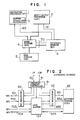
- the requester 62 comprises, as shown in Fig. 5, an MS address register 621 and an MS request controller 622.
- the requester 63 comprises, as shown in Fig. 6, an ES address register 631 and ES request controller 632.
- the requesters 62 and 63 execute the transfer of 256-byte data by being activated by the transfer controller 614.
- the MS requester 62 sets in the register 621 and MS address sent from the selector 613, and operates on its MS request controller 622 to analyze the command from the transfer controller 614.
- the ES requester 63 sets the ES address in the register 631, and operates on its ES request controller 632 to analyze the command.
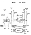
- the data buffer 64 comprises, as shown in Fig. 7, a buffer quantity register 641, an adder/subtracter 642, a buffer quantity controller 643 which controls the requesters 62 and 63 depending on the quantity of buffer, and a buffer 644 which temporarily holds transferred data.
- the data buffer 64 recognizes the data transfer direction based on the command sent over the line 6141.
- the buffer quantity controller 643 controls the requesters 62 and 63 using the lines 6421 and 6431 so that the data transfer source prevents the overflow of buffer 644 when its contents reach a certain level and the data transfer destination holds the issuance of request until a certain amount of data is stacked in the buffer 644.
- the above-mentioned certain level of buffer is controlled depending on the data transfer direction.
- the requester 62 responds to the activation by the transfer controller 614 to send immediately, in case of the data transfer source being MS (accordivelyingly, the destination is ES), the command from the MS request controller 622 together with the MS address in the register 621 to the WS over the line 7011, and issues a read request.
- the requester 63 holds the issuance of request to the ESD 65 until it is informed by the buffer 64 over the line 6431 that a specified amount of data is stacked in the buffer 644.
- the data buffer 64 when readout data is sent from the WS 4 over the line 7042 in response to the read request, writes the readout data in the buffer 644, with an acknowledgement sent over the line 703 in synchronism with the data being a buffer write request.
- the adder/subtracter 642 increments the buffer quantity register 641 by one.
- the buffer quantity controller 643 examines the contents of the updated buffer quantity register 641 to judge whether the specified amount of data is stacked in the buffer 644.
- the buffer 64 repeates the above operations at each reception of readout data.
- the buffer quantity controller 643 When the specified amount of data has been stacked in the buffer 644, the buffer quantity controller 643 indicates it to the requester 63 over the line 6431. In response to this signal, the requester 63 issues a buffer read request to the buffer over the line 6431, sends the command from the ES request controller 632 together with the ES address in the register 631 to the ESD 65, and issues a write request. At this time, the buffer 64 responds to the buffer read request of the requester 63 to read out the transfer data from the buffer 644 and sends it as write data to the ESD 65 over the line 7061. At the same time, the adder/subtracter 642 subtracts by 32 the contents of buffer quantity register 641. The subtrahend "32" is determined on the basis that the write request to the buffer 644 is 8-byte units, whereas the read request is 256-byte units, i.e., 32 fold.
- the requester 63 responds to the activation by the transfer controller 614 to send immediately the ES address and command to the ESD 65, and issues a read request.
- the requester 62 holds the issuance of request to the WS 4 until it is informed by the buffer 64 over the line 6421 that a specified amount of data is stacked in the buffer 644.
- the data buffer 64 when readout data is sent from the ESD 65 over the line 7062 in response to the read request, writes the readout data in the buffer 644, with an acknowledgement sent over the line 653 in synchronism with the data being a buffer write request.
- the buffer quantity register 641 has its contents incremented by one, and the buffer quantity controller 643 examines whether the specified amount of data is stacked in the buffer 644.
- the buffer quantity controller 643 When the specified amount of data has been stacked in the buffer 644, the buffer quantity controller 643 indicates it to the requester 62 over the line 6421. In response to this signal, the requester 62 issues a buffer read request to the buffer over the line 6241, sends the MS address and command to the WS 4, and issues a write request. At this time, the buffer 64 responds to the buffer read request of the requester 62 to read out the transfer data from the buffer 644 and sends it as write data to the WS over the line 7041. At the same time, the adder/subtracter 642 subtracts by 32 the contents of buffer quantity register 641.
- the requesters 62 and 63 In response to the delivery of the termination of requests from the WS 4 and ESD 65 to the requesters 62 and 64 over the lines 702 and 652, respectively, the requesters 62 and 63 indicate the end of data transfers, which have been initiated by the transfer controller 614, to the transfer controller 614 over the lines 6211 and 6311. Receiving the termination signals from both requesters 62 and 63, the transfer controller 614 tests the transfer end on the line 6108 from the selector 613, and, if it is "1" indicative of zero transfer remainder, indicates it to the originating processor over the line 802 or 812. If the line 6108 is "0", the transfer controller 614 activates the requesters 62 and 63 and buffer 64 to execute the data transfer by following the foregoing procedure.
- the WS 4 comprises, as shown in Fig. 8, a command controller 41, an address controller 42, a write data controller 43, a work storage address controller 44, a work storage device 45 (will be termed WSD), an MS requester 46, a buffer memory cancellation controller 47, and a readout data controller 48.
- the WS 4 has a pair of data transfer paths for IP 1 and IOP 2, as in the conventional system, which is added by the third data transfer path for the ES 6, so that it can deal with requests from ES 6 as well as those from the IP 1 and IOP 2.
- the WS 4 shown in Fig. 8 sets the command and MS address sent from the requester 62 over the lines 7011 and 7012 in the command controller 41 and address controller 42, respectively.
- write data from the data buffer 64 is further entered to the data controller 43 over the line 7041.
- the command from the ES 6 entered in the command controller 41 is added to commands from the IP 1 and IOP 2 for selection based on the prescribed rule. If the command from the ES 6 is selected, the WS 4 processes the request from the ES 6 in accordance with this command, the MS address from the requester 62 entered in the address controller 42 and write data from the data buffer 64 entered in the write data controller 43 at the time of write request.
- the WS 4 is assumed to make a copy of MS in a 256-byte unit and generate a request to the MS 5 in a 256-byte unit.
- the WS 4 in case of the request from ES 6 being a read request, first enters the MS address 421 in the work address controller 44 to examine whether it has a copy of data of the MS address. If the data is found copied, the work storage address controller 44 reads out the data from the WSD 45 over the line 441. At this time, the address of the WSD 45 is part of the MS address 421 and on the line 442 for the rest. The data 451 read out of the WSD 45 is sent, together with the acknowledgement from the readout data controller 48 onto the line 703, to the data buffer 64 over the line 7042. In case the line 411 indicates that the invalidation or retardation of copy of the data is specified by the command, the work storage address controller 44, after the above-mentioned examination of copy, resets the copy valid bit to "0".
- the work storage address controller 44 if data of the MS address is not copied, operates on the MS requester 46 over the line 441 to issue a read request to the MS 5. In this case, the MS address 421 is used.
- the MS requester 46 sends the command and MS address to the MS 5 over the lines 4501 and 4502, and issues a read request.
- the MS 5 responds to the read request to send back readout data and acknowledgement in synchronism with the data.
- the work storage address controller 44 makes a new copy of the data as data of the MS address, and the readout data controller 48 sends the data to the data buffer 64 over the line 7042, while at the same time making acknowledgement to the line 703.
- the work storage address controller 44 gets a new storage location in the WSD 45 in accordance with the widely-known LRU (Least Recently Used) algorithm, and writes the readout data 5402 on the line 441 into the WSD 45.
- the address of WSD 45 indicative of the newly established storage location is given as part of the MS address 421 and on the line 442 for the rest.
- the work storage address controller 44 does not make the copy, and accordingly does not execute the writing to the WSD 45.
- the WS 4 enters the MS address 421 to the work storage address controller 44 to examine whether data of the MS address is copied. If the data is copied, the work storage address controller 44 writes write data 431 into the WSD 45 over the line 441. Also in this case, the address of the WSD 45 is given as part of the MS address 421 and the line 442.
- the work storage address controller 44 If the line 411 indicates that the invalidation or retardation of the copy of the data is specified by the command, the work storage address controller 44 resets the copy valid bit to "0", and operates on the MS requester 46 over the line 441 to issue a write request to the MS 5, instead of writing the write data 431 into the WSD 45. In this operation, the MS address 421 and write data 431 are used.
- the MS requester 46 sends the command, MS address and write data to the MS 5 over the lines 4501, 4502 and 4503, and issues a write request.
- the work storage address controller 44 makes a new copy of the write data 431 as data of the MS address, and writes the data 431 over the line 441 into a storage location established newly in the WSD 45 in the same manner as the previous case.
- the address of WSD 45 indicative of the new storage location is given as part of the MS address and line 442 for the rest.
- the work storage address controller 44 does not make the copy, and operates on the MS requester 46 over the line 441 to issue a write request to the MS 5, as in the previous case, instead of writing the write data 431 into the WSD 45.
- the WS 4 further examines with the buffer memory cancellation controller 47 the state of copy of data of the MS address to the BS 3 in parallel to the copy examination for the data to the WS 4 by the work storage address controller 44.
- the buffer memory cancellation controller 47 is provided in advance with a front buffer address array (FAA) which stores the copy state of BS 3.
- FAA front buffer address array
- the MS address 421 is entered to the controller 47 to examine whether data of the MS address is copied in the BS 3.
- the buffer memory cancellation controller 47 requests to the IP 1 over the line 4101 the cancellation of copy of the MS address indicated on the line 4102, thereby preventing the data written in the WSD 45 or MS 5 from becoming much newer than the data copied in the BS 3.
- the hierarchical storage system is organized in three ranks of BS 3, WS 4 and MS 5, the invention is also applicable to the system which further includes a storage of another rank controlled in store-in mode located between the WS 4 and MS 5, or a storage controlled in store-through mode located between the BS 3 and WS 4.
Abstract
Description
- This invention relates to an extended storage system for a data processing system, and particularly to an extended storage system suited to transfer data between hierarchical storages and an extended storage.
- U.S. Patent No. 4,476,524 issued to D.T. Braun et al. on October 9, 1984 discloses a data processing system which includes a data transfer path between a main storage (will be termed MS hereinafter) and an extended storage (or page storage) and performs data transfer between the MS and extended storage using the data transfer path.
- As a prior art for improving the adjustment of difference in the operating speed between the processor and MS in a data processing system, JP-A-52-71138 (corresponding to JP-B-57-57782) dicloses hierarchical storages in which a small-capacity, high-speed high ranking storage, e.g., a buffer storage (will be termed BS hereinafter) is provided on the part of the processor, and an intermediate-rank storage, e.g., a work storage (will be termed WS hereinafter) serving as a second-rank buffer, having an intermediate speed and intermediate capacity as compared with the BS and MS is provided between the BS and MS. In this case, the MS in the lowest-rank storage.
- U.S. Patent No. 4,639,862 issued to H. Wada on January 27, 1987 discloses an addressing system for the extended storage. The contents of the above publication are introduced to the present patent application without mentioning specifically.
- In reading out data such as an instructions or operand stored in three or more hierarchical storages, the data is read out from a storage of as high rank as possible which holds the object data or contains a copy of the data. Only if any storage higher in rank than MS does not contain a copy of data, it is read out from the MS. Control is made to memorize data of much usage at a higher rank storage. The processing speed is thus enhanced.
- In writing data into hierarchical storages, data in storages of all ranks are not rewritten at once, but instead altered data is rewritten in a store-in manner for storages below a certain rank. The processing speed is thus enhanced.
- Among control modes of rewriting data in a storage of a certain rank, rewriting data immediately, after rewriting data in the certain rank storage, to the next lower ranking storage in categorized to be "store-through" mode, while rewriting data by returning the data to the next lower ranking storage when the rewrited data in the active storage is no longer used is categorized to be "store-in" mode. In a hierarchical storage system which controls storing into an intermediate storage in store-in mode, the MS which is the lowest-rank storage does not necessarily have its data always updated to the newest state.
- Recent advanced semiconductor technologies have provided higher operating speeds for processors, year after year, whereas MSs have been rendered little progress in the operating speed although their capacities have been increased and their costs lowered. Therefore, the difference of speed between these devices is further increasing.
- In the data processing system disclosed in the above-mentioned U.S. Patent No. 4,476,524, central processors (CPs) and channel processors (CHs) are connected through a system controller (SC) to main storages (MSs), which are connected with page storages (PSs) through an MS/PS data bus.
- An object of this invention is to provide an extended storage system used suitably for transferring data between hierarchical storages of three ranks or more and an extended storage.
- Another object of this invention is to provide an extended storage system which ensures the latest version of copied data by merely having means which, following a data transfer from an extended storage to hierarchical storages, invalidates the copy of transfer destination data among data copied in a storage higher in rank than at least one intermediate-rank storage.
- A further object of this invention is to prevent improper data transfer to the ES from the MS whose contents would not be yet updated to the latest version due to the presence of an intermediate-rank work storage which is controlled in store-in mode and is higher in rank than the MS.
- A further object of this invention is to solve such a problem that, in case of data transfer from the ES to MS and in case that WS or BS higher in rank than the MS has a copy of data that has been stored in the MS until the transfer, the copied data in the WS or BS is inconsistent with the newly transferred data to the MS and the transferred data solely becomes new data.
- According to this invention, the above objectives are achieved through the provision, between at least one intermediate-rank storage controlled in store-in mode and an ES, of a data transfer path for the data transfer between the intermediate-rank storage and the ES, and means of invalidating transfer destination data of the data to be transferred in the hierarchical storages, i.e., portion corresponding to the data to be cancelled because of change in destinated portion, among data copied in a storage higher in rank than the intermediate-rank storage, and there can be achieved a data transfer from the ES to a hierarchical storage made similarly as the data transfer from a processor to the hierarchical storage.
- Further provided is control means which, following a data transfer between the hierarchical storages and ES, invalidates or retards the transferred data in the intermediate-rank storage and storages excluding MS lower in rank than the intermediate-rank storage (intermediate/lower ranking storages). More specifically, if the WS has a copy of data to be cancelled which is already in the MS destination attributable to the transfer from ES to MS, it is cancelled. If the WS does not have a copy of data of MS destination to be cancelled, which case is not a normal store-in operation, an operation to copy the data into the WS is retarded, namely it is not made valid. The discrimination between "valid" and "invalid" can be made using flag means.
- With a data transfer path being provided between the intermediate-rank storage or WS and ES, when data is transferred from the MS or WS among hierarchical storages to the ES, the intermediate-rank storage is first referenced and, if the WS has a copy of the data to be transferred, the data is read out of the intermediate-rank storage and transferred to the ES, or, if the WS does not have the copy, the data is read out of the MS and transferred to the ES. Since storages higher in rank than the intermediate storage or BS are controlled in store-through mode, the transfer data read out as described above is always in the latest version among the WS and the BS.
- With the control means of invalidating or retarding the copy of data to be transferred from the intermediate-storage being activated, if there is a copy of transfer data, each storage within the intermediate-rank storage which has been referenced at reading of the transfer data invalidates the copy after the data has been read out, or, if the copy is absent, retards the copy in the self storage of the data read out from a lower-rank storage.
- In this way, with the control means being activated, when data transfer takes place between hierarchical storages and ES, the intermediate-rank storage can be placed in a state of having no copy of the transfer data, and accordingly for a data transfer of less urgency the control means is activated so that the intermediate storage can be used more efficiently. For an urgent data transfer between the ES and hierarchical storages, the transfer is accompanied by copying by holding the generation of the command which activates the control means.
-
- Fig. 1 is a block diagram of a data processing system provided with the extended storage system according to the invention;
- Fig. 2 is a block diagram showing the arrangement of the
ES 6 in Fig. 1; - Fig. 3 is a block diagram showing the arrangement of the
transfer command controller 61 in Fig. 2; - Fig. 4 is a block diagram showing the arrangement of the
transfer command register 611 in Fig. 3; - Fig. 5 is a block diagram showing the arrangement of the
requester 62 in Fig. 2; - Fig. 6 is a block diagram showing the arrangement of the
requester 63 in Fig. 2; - Fig. 7 is a block diagram showing the arrangement of the
data buffer 64 in Fig. 2; and - Fig. 8 is a block diagram showing the arrangement of the
WS 4 in Fig. 1. - An embodiment of the inventive extended storage system will be described in detail with reference to the drawings.
- In Fig. 1, the inventive extended storage system comprising hierarchical storages including, from higher to lower ranks, a buffer storage (BS) 3, a work storage (WS) 4 and a main storage (MS) 5, and an extended storage (ES) 6, with a
data transfer path 70 being provided between theWS 4 andES 6. The BS 3 and WS 4 are controlled in store-through mode and store-in mode, respectively. An instruction processor (IP) 1 and input/output processor (IOP) 2 dictate and control the data transfer between the WS 4 and ES 6 using an IPcontrol signal line 80 and IOPcontrol signal line 81, respectively. - The
ES 6 comprises an extended storage device (will be termed ESD) 65 which stores data from theWS 4, atransfer controller 61 which controls the transfer commands from theIP 1 andIOP 2,requesters WS 4 andESD 65, and adata buffer 64 which temporarily holds data from the WS 4 and ESD 65. - The
transfer controller 61 comprises, as shown in Fig. 3,transfer command registers IP 1 andIOP 2, aselector 613 which selects the output of thetransfer command register 611 or 12, and atransfer controller 614 which generally controls data transfer. - The
transfer command register 611 comprise, as shown in Fig. 4, acommand register 6111, atransfer volume register 6112, anMS address register 6113, anES address register 6114, asubtracter 6115,adders 6116 and 6117, and atransfer end tester 6118 which detects that thetransfer volume register 6112 becomes "empty". Thetransfer command register 612 has the same arrangement as 611. - Commands of data transfer between
WS 4 andES 6 are sent to theES 6 over thetransfer command lines IP 1, or depending on the channel command word (CCW) for a command from theIOP 2. The command contains the transfer direction between theWS 4 andES 6, the specification of activation for the control means of copy invalidation/retardation to theWS 4, the MS address and ES address indicative of the starting addresses of the transfer source and transfer destination. - Commands sent from the
IP 1 are set in the respective registers 6111-6114 in thetransfer command register 611, while command sent from theIOP 2 are set in the respective registers in thetransfer command register 612. A command set in thetransfer command register transfer controller 614 overcommand line transfer controller 614 selects one of the command sources based on the prescribed rule and operates on theselector 613 to distribute thetransfer end signal 6108,MS address 6122 andES address 6132 from the selected transfer command register to the respective blocks so that the transfer operation is executed in accordance with the contents of the selected transfer command register. - Initially, the
transfer controller 614 tests thetransfer end signal 6108 and, if it is "1" indicative of "zero transfer remainder", indicates the end of transfer to the originating processor over theline transfer end signal 6108 is "0", thecontroller 614 analyzes the selected command and activates therequesters data buffer 64 using thecommand lines command line 6121 carries such information as transfer direction and copy control, andcommand lines selector 613 delivers the MS address to therequester 62 over theline 6122 and the ES address to therequester 63 over theline 6132. - Following the activation of the
requesters data buffer 64, thetransfer controller 614 directs the transfer command register over theline IP 1 is selected, thetransfer controller 614 instructs thetransfer command register 611 over theline 6101. On receiving the instruction, thetransfer command register 611 operates on thesubtracter 6115 andadders 6116 and 6117 to decrement the contents of thetransfer remainder register 6112 and increment the contents of theMS address register 6113 and ESaddress register 6114, each by one. - The
requester 62 comprises, as shown in Fig. 5, anMS address register 621 and anMS request controller 622. Similarly, the requester 63 comprises, as shown in Fig. 6, an ES address register 631 andES request controller 632. Therequesters transfer controller 614. In response to the activation, the MS requester 62 sets in theregister 621 and MS address sent from theselector 613, and operates on itsMS request controller 622 to analyze the command from thetransfer controller 614. Similarly, the ES requester 63 sets the ES address in the register 631, and operates on itsES request controller 632 to analyze the command. - The
data buffer 64 comprises, as shown in Fig. 7, abuffer quantity register 641, an adder/subtracter 642, abuffer quantity controller 643 which controls therequesters buffer 644 which temporarily holds transferred data. By being activated by thetransfer command controller 61, thedata buffer 64 recognizes the data transfer direction based on the command sent over theline 6141. Thebuffer quantity controller 643 controls therequesters lines buffer 644 when its contents reach a certain level and the data transfer destination holds the issuance of request until a certain amount of data is stacked in thebuffer 644. The above-mentioned certain level of buffer is controlled depending on the data transfer direction. - The requester 62 responds to the activation by the
transfer controller 614 to send immediately, in case of the data transfer source being MS (accordingly, the destination is ES), the command from theMS request controller 622 together with the MS address in theregister 621 to the WS over theline 7011, and issues a read request. The requester 63 holds the issuance of request to theESD 65 until it is informed by thebuffer 64 over theline 6431 that a specified amount of data is stacked in thebuffer 644. Thedata buffer 64, when readout data is sent from theWS 4 over theline 7042 in response to the read request, writes the readout data in thebuffer 644, with an acknowledgement sent over theline 703 in synchronism with the data being a buffer write request. At this time, the adder/subtracter 642 increments thebuffer quantity register 641 by one. Thebuffer quantity controller 643 examines the contents of the updatedbuffer quantity register 641 to judge whether the specified amount of data is stacked in thebuffer 644. Thebuffer 64 repeates the above operations at each reception of readout data. - When the specified amount of data has been stacked in the
buffer 644, thebuffer quantity controller 643 indicates it to the requester 63 over theline 6431. In response to this signal, the requester 63 issues a buffer read request to the buffer over theline 6431, sends the command from theES request controller 632 together with the ES address in the register 631 to theESD 65, and issues a write request. At this time, thebuffer 64 responds to the buffer read request of the requester 63 to read out the transfer data from thebuffer 644 and sends it as write data to theESD 65 over theline 7061. At the same time, the adder/subtracter 642 subtracts by 32 the contents ofbuffer quantity register 641. The subtrahend "32" is determined on the basis that the write request to thebuffer 644 is 8-byte units, whereas the read request is 256-byte units, i.e., 32 fold. - In case of the data transfer source being ES (accordingly, the destination is MS), the requester 63 responds to the activation by the
transfer controller 614 to send immediately the ES address and command to theESD 65, and issues a read request. The requester 62 holds the issuance of request to theWS 4 until it is informed by thebuffer 64 over theline 6421 that a specified amount of data is stacked in thebuffer 644. Thedata buffer 64, when readout data is sent from theESD 65 over theline 7062 in response to the read request, writes the readout data in thebuffer 644, with an acknowledgement sent over theline 653 in synchronism with the data being a buffer write request. Thebuffer quantity register 641 has its contents incremented by one, and thebuffer quantity controller 643 examines whether the specified amount of data is stacked in thebuffer 644. - When the specified amount of data has been stacked in the
buffer 644, thebuffer quantity controller 643 indicates it to the requester 62 over theline 6421. In response to this signal, the requester 62 issues a buffer read request to the buffer over theline 6241, sends the MS address and command to theWS 4, and issues a write request. At this time, thebuffer 64 responds to the buffer read request of the requester 62 to read out the transfer data from thebuffer 644 and sends it as write data to the WS over theline 7041. At the same time, the adder/subtracter 642 subtracts by 32 the contents ofbuffer quantity register 641. - In response to the delivery of the termination of requests from the
WS 4 andESD 65 to therequesters lines requesters transfer controller 614, to thetransfer controller 614 over thelines requesters transfer controller 614 tests the transfer end on theline 6108 from theselector 613, and, if it is "1" indicative of zero transfer remainder, indicates it to the originating processor over theline line 6108 is "0", thetransfer controller 614 activates therequesters buffer 64 to execute the data transfer by following the foregoing procedure. - Next, the operation of the
WS 4 upon receiving a request from the requester 62 will be described. TheWS 4 comprises, as shown in Fig. 8, acommand controller 41, anaddress controller 42, awrite data controller 43, a workstorage address controller 44, a work storage device 45 (will be termed WSD), anMS requester 46, a buffermemory cancellation controller 47, and areadout data controller 48. TheWS 4 has a pair of data transfer paths forIP 1 andIOP 2, as in the conventional system, which is added by the third data transfer path for theES 6, so that it can deal with requests fromES 6 as well as those from theIP 1 andIOP 2. - When the
ES 6 issues a request to theWS 4, theWS 4 shown in Fig. 8 sets the command and MS address sent from the requester 62 over thelines command controller 41 andaddress controller 42, respectively. For a write request, write data from thedata buffer 64 is further entered to thedata controller 43 over theline 7041. The command from theES 6 entered in thecommand controller 41 is added to commands from theIP 1 andIOP 2 for selection based on the prescribed rule. If the command from theES 6 is selected, theWS 4 processes the request from theES 6 in accordance with this command, the MS address from the requester 62 entered in theaddress controller 42 and write data from thedata buffer 64 entered in thewrite data controller 43 at the time of write request. TheWS 4 is assumed to make a copy of MS in a 256-byte unit and generate a request to theMS 5 in a 256-byte unit. - The
WS 4, in case of the request fromES 6 being a read request, first enters theMS address 421 in thework address controller 44 to examine whether it has a copy of data of the MS address. If the data is found copied, the workstorage address controller 44 reads out the data from theWSD 45 over theline 441. At this time, the address of theWSD 45 is part of theMS address 421 and on theline 442 for the rest. Thedata 451 read out of theWSD 45 is sent, together with the acknowledgement from thereadout data controller 48 onto theline 703, to thedata buffer 64 over theline 7042. In case the line 411 indicates that the invalidation or retardation of copy of the data is specified by the command, the workstorage address controller 44, after the above-mentioned examination of copy, resets the copy valid bit to "0". - The work
storage address controller 44, if data of the MS address is not copied, operates on the MS requester 46 over theline 441 to issue a read request to theMS 5. In this case, theMS address 421 is used. The MS requester 46 sends the command and MS address to theMS 5 over thelines MS 5 responds to the read request to send back readout data and acknowledgement in synchronism with the data. Then, the workstorage address controller 44 makes a new copy of the data as data of the MS address, and thereadout data controller 48 sends the data to thedata buffer 64 over theline 7042, while at the same time making acknowledgement to theline 703. At this stage of copying, the workstorage address controller 44 gets a new storage location in theWSD 45 in accordance with the widely-known LRU (Least Recently Used) algorithm, and writes thereadout data 5402 on theline 441 into theWSD 45. The address ofWSD 45 indicative of the newly established storage location is given as part of theMS address 421 and on theline 442 for the rest. However, in case the line 411 indicates that the invalidation or retardation of the copy of the data is specified by the command, the workstorage address controller 44 does not make the copy, and accordingly does not execute the writing to theWSD 45. - Next, the operation of the
WS 4, in case of the request from theES 6 being a write request, will be described. Initially, theWS 4 enters theMS address 421 to the workstorage address controller 44 to examine whether data of the MS address is copied. If the data is copied, the workstorage address controller 44 writes writedata 431 into theWSD 45 over theline 441. Also in this case, the address of theWSD 45 is given as part of theMS address 421 and theline 442. If the line 411 indicates that the invalidation or retardation of the copy of the data is specified by the command, the workstorage address controller 44 resets the copy valid bit to "0", and operates on the MS requester 46 over theline 441 to issue a write request to theMS 5, instead of writing thewrite data 431 into theWSD 45. In this operation, theMS address 421 and writedata 431 are used. The MS requester 46 sends the command, MS address and write data to theMS 5 over thelines - If data of the MS address is not copied, the work
storage address controller 44 makes a new copy of thewrite data 431 as data of the MS address, and writes thedata 431 over theline 441 into a storage location established newly in theWSD 45 in the same manner as the previous case. In this operation, the address ofWSD 45 indicative of the new storage location is given as part of the MS address andline 442 for the rest. However, in case the line 411 indicates that the invalidation or retardation of the copy of the data is specified by the command, the workstorage address controller 44 does not make the copy, and operates on the MS requester 46 over theline 441 to issue a write request to theMS 5, as in the previous case, instead of writing thewrite data 431 into theWSD 45. - In case of the request from the
ES 6 being a write request, theWS 4 further examines with the buffermemory cancellation controller 47 the state of copy of data of the MS address to theBS 3 in parallel to the copy examination for the data to theWS 4 by the workstorage address controller 44. The buffermemory cancellation controller 47 is provided in advance with a front buffer address array (FAA) which stores the copy state ofBS 3. In this case, theMS address 421 is entered to thecontroller 47 to examine whether data of the MS address is copied in theBS 3. If the data is found copied, the buffermemory cancellation controller 47 requests to theIP 1 over theline 4101 the cancellation of copy of the MS address indicated on theline 4102, thereby preventing the data written in theWSD 45 orMS 5 from becoming much newer than the data copied in theBS 3. - Although in the foregoing embodiment of this invention, the hierarchical storage system is organized in three ranks of
BS 3,WS 4 andMS 5, the invention is also applicable to the system which further includes a storage of another rank controlled in store-in mode located between theWS 4 andMS 5, or a storage controlled in store-through mode located between theBS 3 andWS 4.
Claims (7)
valid flag means (44) which is provided for said work storage and adapted to indicate the validity of part of said main storage held in said work storage;
and
a command controller (41) which issues to said flag means a signal (411) indicative of the validity of data in said work storage related to data to be transferred, in accordance with a transfer command for said extended storage issued by said instruction processor.
a buffer storage cancellation controller (47) which is connected to said command controller and adapted to control the cancellation of part of data in said buffer storage; and
a buffer address array (BAA) which is provided in said buffer storage and adapted to control the validity of a copy, from said main storage, of data corresponding to part of address in said buffer storage, on the basis of the output of said buffer storage cancellation controller provided in said buffer storage.
means (6111-6114) of holding the number of words of data transferred to/from said work storage over said transfer path, the starting address of said extended storage, the starting address of said main storage and said transfer command; and
means (6115-6117) of updating said starting addresses and said number of words at a transfer to/from said extended storage.
an extended storage (6); and
a data transfer path (70) provided between said intermediate-rank storage and said extended storage for implementing data transfer between said hierarchical storages and said extended storage in accordance with a command from said instruction processor or said input/output processor.
Applications Claiming Priority (2)
| Application Number | Priority Date | Filing Date | Title |
|---|---|---|---|
| JP37437/88 | 1988-02-22 | ||
| JP63037437A JP2965987B2 (en) | 1988-02-22 | 1988-02-22 | Data processing system |
Publications (3)
| Publication Number | Publication Date |
|---|---|
| EP0330087A2 true EP0330087A2 (en) | 1989-08-30 |
| EP0330087A3 EP0330087A3 (en) | 1991-05-15 |
| EP0330087B1 EP0330087B1 (en) | 1995-11-22 |
Family
ID=12497492
Family Applications (1)
| Application Number | Title | Priority Date | Filing Date |
|---|---|---|---|
| EP89102752A Expired - Lifetime EP0330087B1 (en) | 1988-02-22 | 1989-02-17 | Extended storage system |
Country Status (5)
| Country | Link |
|---|---|
| US (2) | US5307461A (en) |
| EP (1) | EP0330087B1 (en) |
| JP (1) | JP2965987B2 (en) |
| CA (1) | CA1319200C (en) |
| DE (1) | DE68924860T2 (en) |
Cited By (2)
| Publication number | Priority date | Publication date | Assignee | Title |
|---|---|---|---|---|
| WO2001095106A2 (en) * | 2000-06-02 | 2001-12-13 | Sun Microsystems, Inc. | Virtual heap for a virtual machine |
| US6934755B1 (en) | 2000-06-02 | 2005-08-23 | Sun Microsystems, Inc. | System and method for migrating processes on a network |
Families Citing this family (6)
| Publication number | Priority date | Publication date | Assignee | Title |
|---|---|---|---|---|
| JP2965987B2 (en) * | 1988-02-22 | 1999-10-18 | 株式会社日立製作所 | Data processing system |
| JPH04305741A (en) * | 1991-04-02 | 1992-10-28 | Nec Corp | Data base input/output control system |
| US5603046A (en) * | 1993-11-02 | 1997-02-11 | Motorola Inc. | Method for complex data movement in a multi-processor data processing system |
| US20050086430A1 (en) * | 2003-10-17 | 2005-04-21 | International Business Machines Corporation | Method, system, and program for designating a storage group preference order |
| WO2009155463A2 (en) * | 2008-06-20 | 2009-12-23 | Leostream Corp | Management layer method and apparatus for dynamic assignment of users to computer resources |
| US8793449B1 (en) | 2009-10-16 | 2014-07-29 | Netapp, Inc. | Storage subsystem including logic for copy-out and write |
Citations (3)
| Publication number | Priority date | Publication date | Assignee | Title |
|---|---|---|---|---|
| EP0165823A2 (en) * | 1984-06-22 | 1985-12-27 | Fujitsu Limited | Tag control circuit for buffer storage |
| EP0173893A2 (en) * | 1984-08-24 | 1986-03-12 | International Business Machines Corporation | Computing system and method providing working set prefetch for level two caches |
| EP0214870A2 (en) * | 1985-09-12 | 1987-03-18 | Fujitsu Limited | System for controlling a data transfer instruction with an extension storage device |
Family Cites Families (18)
| Publication number | Priority date | Publication date | Assignee | Title |
|---|---|---|---|---|
| US4055851A (en) * | 1976-02-13 | 1977-10-25 | Digital Equipment Corporation | Memory module with means for generating a control signal that inhibits a subsequent overlapped memory cycle during a reading operation portion of a reading memory cycle |
| US4075686A (en) * | 1976-12-30 | 1978-02-21 | Honeywell Information Systems Inc. | Input/output cache system including bypass capability |
| US4521850A (en) * | 1977-12-30 | 1985-06-04 | Honeywell Information Systems Inc. | Instruction buffer associated with a cache memory unit |
| US4189770A (en) * | 1978-03-16 | 1980-02-19 | International Business Machines Corporation | Cache bypass control for operand fetches |
| US4399503A (en) * | 1978-06-30 | 1983-08-16 | Bunker Ramo Corporation | Dynamic disk buffer control unit |
| JPS5757782A (en) * | 1980-09-26 | 1982-04-07 | Nippon Kokan Kk <Nkk> | Quenching furnace of dry-process quenching apparatus for coke |
| US4394732A (en) * | 1980-11-14 | 1983-07-19 | Sperry Corporation | Cache/disk subsystem trickle |
| US4476524A (en) * | 1981-07-02 | 1984-10-09 | International Business Machines Corporation | Page storage control methods and means |
| US4464712A (en) * | 1981-07-06 | 1984-08-07 | International Business Machines Corporation | Second level cache replacement method and apparatus |
| US4429385A (en) * | 1981-12-31 | 1984-01-31 | American Newspaper Publishers Association | Method and apparatus for digital serial scanning with hierarchical and relational access |
| US4442487A (en) * | 1981-12-31 | 1984-04-10 | International Business Machines Corporation | Three level memory hierarchy using write and share flags |
| US4499539A (en) * | 1982-12-20 | 1985-02-12 | International Business Machines Corporation | Method and apparatus for limiting allocated data-storage space in a data-storage unit |
| JPS59167761A (en) * | 1983-03-14 | 1984-09-21 | Hitachi Ltd | Computer system |
| JPS60134953A (en) * | 1983-12-23 | 1985-07-18 | Hitachi Ltd | Data transfer controller |
| JPS62263550A (en) * | 1986-05-09 | 1987-11-16 | Fujitsu Ltd | Cache memory invalidating system |
| JPS6364144A (en) * | 1986-09-04 | 1988-03-22 | Hitachi Ltd | Inter-memory data transfer system |
| JP2965987B2 (en) * | 1988-02-22 | 1999-10-18 | 株式会社日立製作所 | Data processing system |
| US4905188A (en) * | 1988-02-22 | 1990-02-27 | International Business Machines Corporation | Functional cache memory chip architecture for improved cache access |
-
1988
- 1988-02-22 JP JP63037437A patent/JP2965987B2/en not_active Expired - Lifetime
-
1989
- 1989-02-17 DE DE68924860T patent/DE68924860T2/en not_active Expired - Lifetime
- 1989-02-17 EP EP89102752A patent/EP0330087B1/en not_active Expired - Lifetime
- 1989-02-21 CA CA000591582A patent/CA1319200C/en not_active Expired - Lifetime
-
1992
- 1992-09-24 US US07/950,745 patent/US5307461A/en not_active Expired - Lifetime
-
1993
- 1993-12-29 US US08/175,285 patent/US5471582A/en not_active Expired - Lifetime
Patent Citations (3)
| Publication number | Priority date | Publication date | Assignee | Title |
|---|---|---|---|---|
| EP0165823A2 (en) * | 1984-06-22 | 1985-12-27 | Fujitsu Limited | Tag control circuit for buffer storage |
| EP0173893A2 (en) * | 1984-08-24 | 1986-03-12 | International Business Machines Corporation | Computing system and method providing working set prefetch for level two caches |
| EP0214870A2 (en) * | 1985-09-12 | 1987-03-18 | Fujitsu Limited | System for controlling a data transfer instruction with an extension storage device |
Non-Patent Citations (1)
| Title |
|---|
| PROCEEDINGS OF THE IFIP 9TH WORLD COMPUTER CONGRESS, Paris, 19th - 23rd September 1983, pages 693-697, North-Holland, Amsterdam, NL; A. HATTORI et al.: "Three-level hierarchical storage system for FACOM M-380/382" * |
Cited By (3)
| Publication number | Priority date | Publication date | Assignee | Title |
|---|---|---|---|---|
| WO2001095106A2 (en) * | 2000-06-02 | 2001-12-13 | Sun Microsystems, Inc. | Virtual heap for a virtual machine |
| WO2001095106A3 (en) * | 2000-06-02 | 2003-01-30 | Sun Microsystems Inc | Virtual heap for a virtual machine |
| US6934755B1 (en) | 2000-06-02 | 2005-08-23 | Sun Microsystems, Inc. | System and method for migrating processes on a network |
Also Published As
| Publication number | Publication date |
|---|---|
| US5307461A (en) | 1994-04-26 |
| EP0330087A3 (en) | 1991-05-15 |
| JPH01213732A (en) | 1989-08-28 |
| CA1319200C (en) | 1993-06-15 |
| US5471582A (en) | 1995-11-28 |
| EP0330087B1 (en) | 1995-11-22 |
| DE68924860D1 (en) | 1996-01-04 |
| DE68924860T2 (en) | 1996-04-18 |
| JP2965987B2 (en) | 1999-10-18 |
Similar Documents
| Publication | Publication Date | Title |
|---|---|---|
| CA1124888A (en) | Integrated multilevel storage hierarchy for a data processing system with improved channel to memory write capability | |
| US5276836A (en) | Data processing device with common memory connecting mechanism | |
| US6226695B1 (en) | Information handling system including non-disruptive command and data movement between storage and one or more auxiliary processors | |
| US6260117B1 (en) | Method for increasing efficiency in a multi-processor system and multi-processor system with increased efficiency | |
| EP0405882A2 (en) | Move 16 block move and coprocessor interface instruction | |
| US5502825A (en) | Data processing system with an enhanced cache memory control | |
| US6065099A (en) | System and method for updating the data stored in a cache memory attached to an input/output system | |
| US6119150A (en) | Message passing distributed shared memory system that eliminates unnecessary software controlled cache flushes or purges | |
| EP0330087B1 (en) | Extended storage system | |
| KR100505695B1 (en) | Cache memory device having dynamically-allocated or deallocated buffers, digital data processing system comprising it and method thereof | |
| US6507894B1 (en) | Information processing apparatus and process | |
| JP3626609B2 (en) | Multiprocessor system | |
| US6934810B1 (en) | Delayed leaky write system and method for a cache memory | |
| US6401173B1 (en) | Method and apparatus for optimizing bcache tag performance by inferring bcache tag state from internal processor state | |
| EP0631236B1 (en) | A bus-master computer system and method | |
| JP2504323B2 (en) | System bus control method | |
| JP2502406B2 (en) | Storage control system and data processing device | |
| JPH0628258A (en) | Microprocessor | |
| JPS63247852A (en) | Cache memory control method | |
| JPH0816467A (en) | Arithmetic processor with write-back cache memory | |
| KR970004520B1 (en) | High speed memory control method and apparatus | |
| JPS62226348A (en) | Main memory and concurrently main memory control device | |
| JPH05189313A (en) | Cache memory control system | |
| JPH01281545A (en) | Cache memory control system | |
| JPH06274416A (en) | Cache memory device |
Legal Events
| Date | Code | Title | Description |
|---|---|---|---|
| PUAI | Public reference made under article 153(3) epc to a published international application that has entered the european phase |
Free format text: ORIGINAL CODE: 0009012 |
|
| AK | Designated contracting states |
Kind code of ref document: A2 Designated state(s): DE FR GB |
|
| 17P | Request for examination filed |
Effective date: 19901119 |
|
| PUAL | Search report despatched |
Free format text: ORIGINAL CODE: 0009013 |
|
| AK | Designated contracting states |
Kind code of ref document: A3 Designated state(s): DE FR GB |
|
| 17Q | First examination report despatched |
Effective date: 19930705 |
|
| GRAA | (expected) grant |
Free format text: ORIGINAL CODE: 0009210 |
|
| AK | Designated contracting states |
Kind code of ref document: B1 Designated state(s): DE FR GB |
|
| REF | Corresponds to: |
Ref document number: 68924860 Country of ref document: DE Date of ref document: 19960104 |
|
| ET | Fr: translation filed | ||
| PLBE | No opposition filed within time limit |
Free format text: ORIGINAL CODE: 0009261 |
|
| STAA | Information on the status of an ep patent application or granted ep patent |
Free format text: STATUS: NO OPPOSITION FILED WITHIN TIME LIMIT |
|
| 26N | No opposition filed | ||
| REG | Reference to a national code |
Ref country code: GB Ref legal event code: IF02 |
|
| PGFP | Annual fee paid to national office [announced via postgrant information from national office to epo] |
Ref country code: GB Payment date: 20080114 Year of fee payment: 20 |
|
| PGFP | Annual fee paid to national office [announced via postgrant information from national office to epo] |
Ref country code: DE Payment date: 20080307 Year of fee payment: 20 Ref country code: FR Payment date: 20080111 Year of fee payment: 20 |
|
| REG | Reference to a national code |
Ref country code: GB Ref legal event code: PE20 Expiry date: 20090216 |
|
| PG25 | Lapsed in a contracting state [announced via postgrant information from national office to epo] |
Ref country code: GB Free format text: LAPSE BECAUSE OF EXPIRATION OF PROTECTION Effective date: 20090216 |