EP0329140A2 - Exposure control system for full field photolithography using pulsed sources - Google Patents
Exposure control system for full field photolithography using pulsed sources Download PDFInfo
- Publication number
- EP0329140A2 EP0329140A2 EP89102687A EP89102687A EP0329140A2 EP 0329140 A2 EP0329140 A2 EP 0329140A2 EP 89102687 A EP89102687 A EP 89102687A EP 89102687 A EP89102687 A EP 89102687A EP 0329140 A2 EP0329140 A2 EP 0329140A2
- Authority
- EP
- European Patent Office
- Prior art keywords
- exposure
- light source
- attenuation
- control system
- pulsed
- Prior art date
- Legal status (The legal status is an assumption and is not a legal conclusion. Google has not performed a legal analysis and makes no representation as to the accuracy of the status listed.)
- Granted
Links
- 238000000206 photolithography Methods 0.000 title abstract description 5
- 230000001186 cumulative effect Effects 0.000 claims description 11
- 230000002238 attenuated effect Effects 0.000 claims description 8
- 238000005315 distribution function Methods 0.000 claims description 3
- 239000003574 free electron Substances 0.000 claims description 2
- 238000012544 monitoring process Methods 0.000 claims description 2
- 230000004936 stimulating effect Effects 0.000 claims 3
- 238000013459 approach Methods 0.000 claims 2
- 238000004364 calculation method Methods 0.000 claims 2
- 230000000638 stimulation Effects 0.000 claims 1
- 230000005540 biological transmission Effects 0.000 description 7
- 238000000034 method Methods 0.000 description 6
- 238000010304 firing Methods 0.000 description 5
- 230000003287 optical effect Effects 0.000 description 4
- 238000000576 coating method Methods 0.000 description 2
- 230000006870 function Effects 0.000 description 2
- 239000000463 material Substances 0.000 description 2
- 150000001875 compounds Chemical class 0.000 description 1
- 230000007423 decrease Effects 0.000 description 1
- 238000013461 design Methods 0.000 description 1
- 238000010586 diagram Methods 0.000 description 1
- 230000000694 effects Effects 0.000 description 1
- 239000010408 film Substances 0.000 description 1
- 238000009501 film coating Methods 0.000 description 1
- 238000005286 illumination Methods 0.000 description 1
- 238000012986 modification Methods 0.000 description 1
- 230000004048 modification Effects 0.000 description 1
- 230000002093 peripheral effect Effects 0.000 description 1
- 238000001259 photo etching Methods 0.000 description 1
- 238000002256 photodeposition Methods 0.000 description 1
- 229920002120 photoresistant polymer Polymers 0.000 description 1
- 239000000758 substrate Substances 0.000 description 1
- 239000010409 thin film Substances 0.000 description 1
- 238000012546 transfer Methods 0.000 description 1
- 238000001429 visible spectrum Methods 0.000 description 1
Images

Classifications
-
- G—PHYSICS
- G03—PHOTOGRAPHY; CINEMATOGRAPHY; ANALOGOUS TECHNIQUES USING WAVES OTHER THAN OPTICAL WAVES; ELECTROGRAPHY; HOLOGRAPHY
- G03F—PHOTOMECHANICAL PRODUCTION OF TEXTURED OR PATTERNED SURFACES, e.g. FOR PRINTING, FOR PROCESSING OF SEMICONDUCTOR DEVICES; MATERIALS THEREFOR; ORIGINALS THEREFOR; APPARATUS SPECIALLY ADAPTED THEREFOR
- G03F7/00—Photomechanical, e.g. photolithographic, production of textured or patterned surfaces, e.g. printing surfaces; Materials therefor, e.g. comprising photoresists; Apparatus specially adapted therefor
- G03F7/70—Microphotolithographic exposure; Apparatus therefor
- G03F7/70008—Production of exposure light, i.e. light sources
- G03F7/70041—Production of exposure light, i.e. light sources by pulsed sources, e.g. multiplexing, pulse duration, interval control or intensity control
-
- G—PHYSICS
- G03—PHOTOGRAPHY; CINEMATOGRAPHY; ANALOGOUS TECHNIQUES USING WAVES OTHER THAN OPTICAL WAVES; ELECTROGRAPHY; HOLOGRAPHY
- G03F—PHOTOMECHANICAL PRODUCTION OF TEXTURED OR PATTERNED SURFACES, e.g. FOR PRINTING, FOR PROCESSING OF SEMICONDUCTOR DEVICES; MATERIALS THEREFOR; ORIGINALS THEREFOR; APPARATUS SPECIALLY ADAPTED THEREFOR
- G03F7/00—Photomechanical, e.g. photolithographic, production of textured or patterned surfaces, e.g. printing surfaces; Materials therefor, e.g. comprising photoresists; Apparatus specially adapted therefor
- G03F7/70—Microphotolithographic exposure; Apparatus therefor
- G03F7/70483—Information management; Active and passive control; Testing; Wafer monitoring, e.g. pattern monitoring
- G03F7/7055—Exposure light control in all parts of the microlithographic apparatus, e.g. pulse length control or light interruption
- G03F7/70558—Dose control, i.e. achievement of a desired dose
Definitions
- the exposed system 40 can be any one of a number of image transfer systems such as the transferring of an image of a mask or reticle on to a photoresist coated substrate for conventional developing, or the image pattern created by the exposed system may be used for a variety of direct photoetching, photoablation, or photodeposition processes.
- variable attenuator 20 is comprised of a wheel 22 attached to motor 24.
- Motor 24 rotates wheel 22 such that individual attenuators 29 can be selectively positioned in the path of the light pulse generated by the pulsed light source 10.
- a hole 26 is positioned along the peripheral portion of wheel 22 so that sensor 28 can detect its position.
- Sensor 28 can be any type of sensor capable of detecting the position of hole 26, such as a photoemitter-detector pair.
- Sensor 28 then communicates the angular position of wheel 22 to controller 50.
- the controller 50 can then cause the pulsed light source to emit a pulse when one of the selected attenuators 29 is positioned in the path of the light pulse.
- a fixed attenuator 60 is also illustrated in Fig. 2 should the pulsed light source 10 emit a pulse of light that has an exposure dose greater than that needed by the exposed system 40. With the attenuator 60 in the path of the emitted light pulse the exposure dose can be attenuated so that multiple light pulses are needed to obtain the required exposure dose. The attenuator wheel 20 can then be positioned to obtain the desired exposure tolerance with the minimum number of shots.
Abstract
Description
- This invention relates generally to accurately controlling exposure in photolithography, and more particularly to optimizing exposure control when noisy pulsed light sources are used.
- Photolithography is a lithographic technique using an image produced by photography for printing on a print-non-print surface. With this technique pulsed light sources can be used to expose a light sensitive surface. Typically, pulsed light sources have a pulse-to pulse energy fluctuation. This pulse-to-pulse fluctuation makes accurate exposure difficult. Pulsed sources are additionally troublesome because the mean energy per shot may drift with time and other factors. This compounds the difficulty in maintaining the correct exposure. Additionally, the correct exposure may not require an integal number of shots which contributes to the already inaccurate exposure. Therefore, there are problems in maintaining correct exposure when using pulsed light sources.
- A common technique used to control the exposure dose is to increase the number of shots or light pulses needed to expose the light sensitive surface. With a large number of shots the fluctuation in each shot is not as critical in maintaining the proper exposure. But, increasing the number of shots increases the time needed for exposure as well as in most situations requires a large attenuation of the pulsed light source. Increasing the number of shots required for exposure can control exposure to within acceptable limits, but is very inefficient.
- Attempts have also been made to control the average pulse energy of the pulsed light source so that it is an exact sub-multiple of the required dose for exposure. This technique requires a pulsed energy source with little noise or pulse-to-pulse energy fluctuation. Even with a low noise pulsed light source the number of shots required to obtain a reasonably accurate exposure dose is large.
- While the above techniques have greatly increased the use of pulsed sources in photolithography and have achieved some degree of control over the exposure dose they have proven to be inefficient exposure systems. The exposure necessary to obtain a reasonably precise exposure dose is time consuming and shortens the lifetime of the pulsed source which is usually measured by the number of shots fired.
- The present invention is directed to a device for precisely controlling the exposure dose in photolithographic systems using pulsed light sources. The pulsed light source is typically a pulsed laser. The pulsed light is directed through a variable attenuator that controllably attenuates the light pulse before illuminating the system to be exposed. A portion of the light pulse is measured by an exposure dose monitor to determine its fluence. A controller connected to the variable attenuator and the pulsed light source uses the fluence information from the exposure dose monitor to determine the minimum attenuation needed to provide the required exposure dose. The controller can consider the pulse-to pulse energy fluctuation of the source in determining the amount of attenuation needed to provide accurate exposure with a minimum number of shots.
- Accordingly, it is an objective of the present invention to provide accurate exposure with a minimum number of shots.
- It is a further objective of the present invention to provide an exposure system tolerant of noisy light pulse sources.
- It is yet another objective of the present invention to provide the maximum fluence per light pulse while minimizing the probability of overexposure.
- It is an advantage of the present invention that the pulsed light source has a longer life.
- It is a further advantage of the present invention that a simpler power supply can be used to control the light source.
- It is yet a further advantage of the present invention that the overall exposure time is reduced resulting in increased system throughput.
- It is a feature of the present invention that the pulsed light source is controllably variably attenuated.
- It is another feature of the present invention that the light source is controlled by the timing of discharge in relation to the position of a rotating attenuation wheel having constant angular velocity.
- These and other objects, advantages, and features will become readily apparent in view of the following more detailed description.
-
- Fig. 1 is a block diagram illustrating the invention;
- Fig. 2 is a pictorial representation of an embodiment of the present invention;
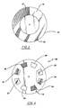
- Fig. 3 is a front elevational view of an attenuation wheel used in one embodiment of the present invention;
- Fig. 4 is a front elevational view of another attenuation wheel used in another embodiment of the present invention.
- Fig. 1 illustrates the present invention. As is shown in Fig. 1, pulsed
light source 10 emits a pulse of light or shot when required. Pulsedlight source 10 is typically a laser, such as an excimer, frequency multiplied, or free-electron laser. The light source can also be a plasma blackbody XUV or an X-ray source. The pulse of light then travels through avariable attenuator 20. Thevariable attenuator 20 can be of any type of material that will predictably attenuate the light pulse or shot. For example, electro-optic modulators, including an acousto-optic and Pockels cell devices, variable spaced Fabry -Perot etalons, partially transmitting meshes and perforated plates, partially transmitting or partially reflecting optical coatings or surfaces, bulk absorbing optical materials, and geometrical measn such as moving blades or shutters. In the case of optical coatings, such as dielectric films, variation of transmission may be obtained by tilting the attenuator elements as well as by interchanging fixed elements or translating elements across the pulsed light which have a transmission gradient. In all of these cases, either step wise attenuation control or continuous variable control is possible. Stepwise attenuation is accomplished by varying portions of theattenuator 20 by discrete intervals of attenuation. These discrete intervals of attenuation can be equal, logarithmic, or any amount that is suitable for the particular application. - After the light pulse passes through the
variable attenuator 20 it entersexposure dose monitor 30. Theexposure dose monitor 30 should not attenuate the transmission of the light pulse more than necessary. The exposure dose monitor 30 detects the fluence leaving thevariable attenuator 20 and being delivered to the exposedsystem 40. A value representative of the fluence transmitted to the exposedsystem 40 is communicated by theexposure dose monitor 30 to thecontroller 50. - The exposed
system 40 can be any one of a number of image transfer systems such as the transferring of an image of a mask or reticle on to a photoresist coated substrate for conventional developing, or the image pattern created by the exposed system may be used for a variety of direct photoetching, photoablation, or photodeposition processes. - The
controller 50 communicates with thepulsed light source 10, thevariable attenuator 20, and the exposure dose monitor 30. Thecontroller 50 uses the information received from theexposure dose monitor 30 to control the cooperation between thevariable attenuator 20 and thepulsed light source 10 to optimize the exposure dose delivered to the exposedsystem 40. Essentially, the controller will select the smallest attenuation available with thevariable attenuator 20 that will, with a high probability, not result in an overexposure by an amount exceeding the exposure tolerance. Thecontroller 50 can also take into account the actual unattenuated pulse energy distribution of the pulsed light source under current conditions. This can be continuously monitored by thecontroller 50 from the information received by theexposure dose monitor 30. - The
controller 50 can be comprised of various well known circuitry. For example, thecontroller 50 can comprise a microprocessor (such as an Intel 80286), together with a numeric co-processor (such as an Intel 80287), program memory, data memory, an analog to digital converter (such as an analog Devices 774 12 bit ADC) for input of data from thepulse energy monitor 30, digital input for monitoring the position of thevariable attenuator 20, digital output for firing thepulsed source 10 and (optionally) for controlling the variable attenuator, and a clock (optionally) for controlling the variable attenuator, and a clock or oscillator among other well known circuitry. - The controller can take the form of a microcomputer, such as an IBM PCAT microcomputer, which can be configured or programmed to perform various functions. Functions that can be accomplished in this way using existing or easily created software and hardware include, but are not limited to; calibrating and storing the degree of attenuation of each attenuating element by comparing mean transmitted energies though the various elements, averaged over many shots of the source; measuring the updating the pulse energy output of the light source (and its pulse energy distribution function) on a continuing basis, and storing same; planning an exposure sequence based on the desired exposure dose, the attenuator calibration, and the stored pulse energy distribution function data; measuring the exposure energy actually delivered to the exposure system on each shot of the pulsed source; computing and storing the cumulative exposure dose following each shot of an exposure sequence; comparing the cumulative dose to the desired total exposure; selecting the attenuation required for the next light source pulse in the exposure sequence; controlling a motor or other means for adjusting or selecting the appropriate attenuation; determining the correct timing the firing the pulsed source so as to achieve the required attenuation, and issuing the firing command at the required time (taking into account the attenuator indexing information from the sensor 28); and finally terminating the exposure sequence when the cumulative exposure reaches the targeted exposure, within specified tolerance bounds.
- For a simple example of how the present invention can reduce the number of shots while maintaining the exposure tolerance consider the following. The pulsed light source operates with a mean unattenuated fluence f with a desired exposure for the system being something greater than f. The pulsed light source is noisy and has a pulse-to-pulse energy fluctuation with a high of 1.1 f and a low of 0.9 f. The
controller 50 begins delivering unattenuated shots or pulses while the exposure dose monitor 30 monitors the cumulative dose. Thecontroller 50 then stops the pulsedlight source 10 from firing when the remaining exposure dose is less than 1.1 f. Thecontroller 50 then positions thevariable attenuator 20 so that it has a transmission value of 1.1 f divided by the remaining exposure dose before instructing the pulsedlight source 10 to deliver a pulse. The exposure does monitor 30 sends information about the last pulse tocontroller 50. A new remaining exposure is calculated and the attenuation is again adjusted to 1.1 f divided by the new remaining exposure dose before thecontroller 50 instructs the pulsedlight source 10 to deliver another pulse. This sequence is repeated until the total exposure is within a specified tolerance band. In the present example, a tolerance of plus or minus 0.5% can be obtained in at most 3 attenuated shots following any unattenuated exposure that might be required. Each additional shot will improve the exposure precision by an order of magnitude. The above example assumes that a continuous variable attenuator is used, but if a stepped attenuator is used a somewhat greater number of shots or pulses is required to reach the same exposure precision. - In Fig. 2 another embodiment of the present invention is illustrated. In Fig. 2 the
variable attenuator 20 is comprised of awheel 22 attached tomotor 24.Motor 24 rotateswheel 22 such thatindividual attenuators 29 can be selectively positioned in the path of the light pulse generated by the pulsedlight source 10. Ahole 26 is positioned along the peripheral portion ofwheel 22 so thatsensor 28 can detect its position.Sensor 28 can be any type of sensor capable of detecting the position ofhole 26, such as a photoemitter-detector pair.Sensor 28 then communicates the angular position ofwheel 22 tocontroller 50. Thecontroller 50 can then cause the pulsed light source to emit a pulse when one of the selectedattenuators 29 is positioned in the path of the light pulse. - Also in Fig. 2 can be seen the
exposure dose monitor 30. Exposure dose monitor 30 comprises abeam splitter 32 anddetector 34. Thebeam splitter 32 redirects a small portion of the light pulse todetector 34 to quantify the energy or exposure dose of that particular light pulse. Ideally, the exposure dose monitor 30 does not affect the exposure dose delivered to the exposedsystem 40. In any event, the small effect that the energy dose monitor could have on the exposure dose delivered to the exposedsystem 40, can be compensated for by thecontroller 50. - A fixed
attenuator 60 is also illustrated in Fig. 2 should the pulsedlight source 10 emit a pulse of light that has an exposure dose greater than that needed by the exposedsystem 40. With theattenuator 60 in the path of the emitted light pulse the exposure dose can be attenuated so that multiple light pulses are needed to obtain the required exposure dose. Theattenuator wheel 20 can then be positioned to obtain the desired exposure tolerance with the minimum number of shots. - Fig. 3 illustrates a type of wheel attenuator that can be used in place of the multiple discrete
step attenuator wheel 22 illustrated in Fig. 2. Thecontinuous attenuator 70 illustrated in Fig. 3 ranges from a high attenuation atportion 72 and continuously decreases in attenuation clockwise around the circumferential portion to a low attenuation atportion 74. This continuously variable transmission attenuator can be used provided that any resulting spatial transmission gradient across the transmitted beam or light pulse is permitted by the optical design of the illumination uniforming optics. The continuously variable transmission attenuator can be fabricated as a multilayer thin film coating. - Fig. 4 illustrates another attenuator wheel that can be used instead of the
wheel 22 illustrated in Fig. 2. Fig. 4 illustrates amultiple cycle wheel 80. The wheel is comprised of two attenuation cycles having three attenuators each.Attenuators 82 have the least attenuation.Attenuators 84 have a larger degree of attenuation thanattenuators 82, and attenuators 85 have the highest degree of attenuation.Non-attenuation portions 88 separate the attenuation cycles onattenuation wheel 80 and do not attenuate the light pulse. The multiple cycles inwheel 80 are used so as not not to unduly restrict the laser firing rate.Wheel 80 permits the laser to fire at least twice for one revolution ofwheel 80. It should be understood that any number of multiple attenuating cycles can be used together with any number of attenuators for each cycle.Holes 26 in Figs. 3 and 4 are used to determine the angular position of the wheels. - While the wheel attenuators in Fig. 3 and 4 have been illustrated with varying degrees of shading this shading is representative of the degree of attenuation of the light pulse at the particular frequency used and need not appear when viewed in the visible spectrum.
- Although the preferred embodiment has been illustrated and described together with other embodiments, it will be obvious to those skilled in the art that various modifications may be made without departing from the spirit and scope of this invention.
Claims (19)
a pulsed light source;
variable attenuation means, placed between said pulsed light source and the system to be exposed, for variably attenuating the light emitted by said pulsed light source;
exposure dose monitor means, placed between said variable attenuation means and the system to be exposed, for monitoring the exposure dose of the attenuated light pulses; and
control means, associated with said exposure dose monitor means, said variable attenuation means, and said pulsed light source, for controlling the attenuation of the light emitted by said pulsed light source by said variable attenuation measn whereby exposure can be accurately controlled with a minimum of light pulses from said pulsed light source.
said pulsed light source is an X-ray source.
said pulsed light source is a plasma blackbody XUV source.
said pulsed light source is a laser.
said laser is an excimer laser.
said laser is a free-electron laser.
said laser is a frequency multiplied laser.
said variable attenuation means comprises a movable continuous attenuation gradient ranging from a high attenuation to a low attenuation.
a wheel,
a plurality of discrete attenuations spaced annularly a predetermined distance apart on said wheel,
means for rotating said wheel; and
means for detecting the angular position of said wheel.
each of said plurality of attenuators have a different attenuation.
each of said plurality of attenuators differ in attenuation by equal logarithmic steps.
said plurality of attenuators are separated into groups of non-attenuating sections.
each of said groups are the same.
a beam splitter; and
a beam detector.
a fixed attenuator positioned in the path of light emitted by said pulsed light source.
said control means further comprises means for determining a cumulative exposure dose delivered by said pulsed light source after being attenuated.
said control means further comprises means for repeatedly calculating the pulsed light source energy distribution function based on recent performance of said pulsed light source.
cumulative dose means, associated with said exposure dose monitor means, for maintaining a cumulative exposure dose of attenuated light pulses emitted by said pulsed light source;
exposure dose calculation means, asociated with said cumulative dose means, for calculating the attenuation needed for next exposure dose in order to fall within a predetermined exposure tolerance;
selection means for selecting an attenuation from said variable attenuation means that most closely approaches the degree of attenuation calculated by said exposure dose calculation means;
attenuation movement means, associated with said variable attenuation means and said selection means, for moving the attenuation selected from said variable attenuation means into the path of light emitted by said pulsed light source; and
pulse stimulation means for controllably stimulating a pulse of light from said pulsed light source.
a pulsed laser light source capable of emitting multiple exposure doses of light which could fluctuate in exposure dose with each pulse;
a wheel having a plurality of openings equally spaced along the circumferential portion, the openings capable of being positioned in the path of light emitted from said pulsed laser light source;
a plurality of attenuators each capable of attenuating differing quantities of the multiple exposure doses, a different one of said plurality of attenuators being placed in each of said plurality of openings;
a motor for rotating said wheel;
sensor means for detecting the angular position of said wheel;
a beam splitter positioned in the path of the multiple exposure doses after being attenuated;
a detector positioned in the path of the portion of the multiple exposure doses diverted by said beam splitter;
cumulative dose means, associated with said detector, for measuring the cumulative exposure dose generated by the attenuated multiple exposure doses;
storage means for storing a pulse energy distribution of a number of prior exposure doses emitted by said pulsed laser light source;
exposure dose calculating means, associated with said cumulative dose means and said storage means, for calculating the attenuation needed for a next exposure dose in order to fall within a predetermined exposure tolerance;
selection means for selecting an attenuator from said plurality of attenuators that most closely approaches the degree of attenuation calculated by said exposure dose calculating means;
motor control means, associated with said selection means and said motor, for positioning the attenuator into the path of light emitted by said pulsed laser light source; and
laser shot stimulating means for stimulating a pulse of light from said pulsed laser light source.
Applications Claiming Priority (2)
| Application Number | Priority Date | Filing Date | Title |
|---|---|---|---|
| US157755 | 1988-02-19 | ||
| US07/157,755 US4804978A (en) | 1988-02-19 | 1988-02-19 | Exposure control system for full field photolithography using pulsed sources |
Publications (3)
| Publication Number | Publication Date |
|---|---|
| EP0329140A2 true EP0329140A2 (en) | 1989-08-23 |
| EP0329140A3 EP0329140A3 (en) | 1989-10-11 |
| EP0329140B1 EP0329140B1 (en) | 1994-06-01 |
Family
ID=22565127
Family Applications (1)
| Application Number | Title | Priority Date | Filing Date |
|---|---|---|---|
| EP89102687A Revoked EP0329140B1 (en) | 1988-02-19 | 1989-02-16 | Exposure control system for full field photolithography using pulsed sources |
Country Status (5)
| Country | Link |
|---|---|
| US (1) | US4804978A (en) |
| EP (1) | EP0329140B1 (en) |
| JP (1) | JPH025063A (en) |
| CA (1) | CA1300717C (en) |
| DE (1) | DE68915564T2 (en) |
Cited By (3)
| Publication number | Priority date | Publication date | Assignee | Title |
|---|---|---|---|---|
| WO2005088382A1 (en) * | 2004-03-16 | 2005-09-22 | Sign-Tronic Ag | Method for establishing a light beam with substantially constant luminous intensity |
| US9823572B2 (en) | 2013-06-18 | 2017-11-21 | Asml Netherlands B.V. | Lithographic method |
| TWI714226B (en) * | 2013-06-18 | 2020-12-21 | 荷蘭商Asml荷蘭公司 | Method of controlling a free electron laser, injector for a free electron laser and related free electron laser, lithographic system and non-transitory computer readable medium |
Families Citing this family (25)
| Publication number | Priority date | Publication date | Assignee | Title |
|---|---|---|---|---|
| DE68927430T2 (en) * | 1988-09-02 | 1997-03-13 | Canon Kk | Exposure device |
| JP2958913B2 (en) * | 1990-05-21 | 1999-10-06 | キヤノン株式会社 | X-ray exposure equipment |
| JPH0620924A (en) * | 1992-07-03 | 1994-01-28 | Nikon Corp | Processing apparatus using laser light source |
| JP2862477B2 (en) * | 1993-06-29 | 1999-03-03 | キヤノン株式会社 | Exposure apparatus and method for manufacturing device using the exposure apparatus |
| JPH08179514A (en) * | 1994-12-22 | 1996-07-12 | Canon Inc | Aligner and exposure method |
| JP3630807B2 (en) * | 1994-12-28 | 2005-03-23 | キヤノン株式会社 | Scanning exposure apparatus and device manufacturing method using the scanning exposure apparatus |
| EP0748009B1 (en) * | 1995-06-05 | 2002-12-04 | Canon Kabushiki Kaisha | Output control method for excimer laser |
| JP3127782B2 (en) * | 1995-06-22 | 2001-01-29 | 双葉電子工業株式会社 | Optical printer |
| JP3391940B2 (en) * | 1995-06-26 | 2003-03-31 | キヤノン株式会社 | Illumination device and exposure device |
| JP3591922B2 (en) * | 1995-07-17 | 2004-11-24 | キヤノン株式会社 | Light intensity measurement device |
| JPH09129550A (en) | 1995-08-30 | 1997-05-16 | Canon Inc | Light exposure and method for manufacturing device using the same |
| KR100210569B1 (en) * | 1995-09-29 | 1999-07-15 | 미따라이 하지메 | Exposure method and exposure apparatus and method for manufacturing device using the same |
| JP3459742B2 (en) * | 1996-01-17 | 2003-10-27 | キヤノン株式会社 | Exposure apparatus and device manufacturing method using the same |
| US6555449B1 (en) * | 1996-05-28 | 2003-04-29 | Trustees Of Columbia University In The City Of New York | Methods for producing uniform large-grained and grain boundary location manipulated polycrystalline thin film semiconductors using sequential lateral solidfication |
| JP4392879B2 (en) | 1998-09-28 | 2010-01-06 | キヤノン株式会社 | Projection exposure apparatus and device manufacturing method |
| JP4065518B2 (en) * | 2002-11-29 | 2008-03-26 | キヤノン株式会社 | Exposure equipment |
| WO2005029551A2 (en) | 2003-09-16 | 2005-03-31 | The Trustees Of Columbia University In The City Of New York | Processes and systems for laser crystallization processing of film regions on a substrate utilizing a line-type beam, and structures of such film regions |
| DE102006038455A1 (en) * | 2006-08-16 | 2008-02-21 | Carl Zeiss Smt Ag | Optical system for semiconductor lithography, has adjusting unit positioning optical component, where contact points of adjusting unit at optical component is selected, such that no moments develop at optical component |
| DE102006060368B3 (en) * | 2006-12-16 | 2008-07-31 | Xtreme Technologies Gmbh | Method and arrangement for stabilizing the mean emitted radiation power of a pulsed operated radiation source |
| WO2011102486A1 (en) | 2010-02-22 | 2011-08-25 | ギガフォトン株式会社 | Laser device for exposure device |
| CN102914945B (en) * | 2011-08-04 | 2015-05-13 | 上海微电子装备有限公司 | Distributed exposure dose control system and method |
| US8563956B1 (en) * | 2012-07-28 | 2013-10-22 | Cymer, Llc | Intracavity loss element for power amplifier |
| NL2015735A (en) * | 2014-12-19 | 2016-09-20 | Asml Netherlands Bv | An Undulator. |
| CN108614396B (en) * | 2018-05-09 | 2021-03-02 | Tcl华星光电技术有限公司 | Slit switching device and method for exposure machine |
| CN110895386B (en) * | 2018-09-13 | 2021-02-26 | 上海微电子装备(集团)股份有限公司 | Light transmittance adjusting device and lighting system |
Citations (4)
| Publication number | Priority date | Publication date | Assignee | Title |
|---|---|---|---|---|
| US4516842A (en) * | 1983-05-02 | 1985-05-14 | Trombert John F | Aperture wheel |
| DE3503273A1 (en) * | 1984-02-01 | 1985-08-08 | Canon K.K., Tokio/Tokyo | EXPOSURE METHOD AND DEVICE |
| DE3504938A1 (en) * | 1984-02-14 | 1985-08-14 | Canon K.K., Tokio/Tokyo | EXPOSURE METHOD AND DEVICE |
| US4711568A (en) * | 1985-03-06 | 1987-12-08 | Canon Kabushiki Kaisha | Exposure apparatus |
Family Cites Families (5)
| Publication number | Priority date | Publication date | Assignee | Title |
|---|---|---|---|---|
| US4264986A (en) * | 1979-03-12 | 1981-04-28 | Willis Craig I | Information-recording process & apparatus |
| GB8425425D0 (en) * | 1984-10-09 | 1984-11-14 | Crosfield Electronics Ltd | Radiation generation apparatus |
| US4613877A (en) * | 1984-11-26 | 1986-09-23 | Data Recording Systems, Inc. | High resolution laser printer |
| US4719474A (en) * | 1985-07-19 | 1988-01-12 | Rudolf Hell Gmbh | Apparatus for imaging text and graphics on photosensitive material |
| JP2524108B2 (en) * | 1986-02-24 | 1996-08-14 | 富士写真フイルム株式会社 | Optical scanning recorder |
-
1988
- 1988-02-19 US US07/157,755 patent/US4804978A/en not_active Expired - Fee Related
-
1989
- 1989-02-07 CA CA000590310A patent/CA1300717C/en not_active Expired - Lifetime
- 1989-02-16 EP EP89102687A patent/EP0329140B1/en not_active Revoked
- 1989-02-16 DE DE68915564T patent/DE68915564T2/en not_active Expired - Lifetime
- 1989-02-20 JP JP1038513A patent/JPH025063A/en active Pending
Patent Citations (4)
| Publication number | Priority date | Publication date | Assignee | Title |
|---|---|---|---|---|
| US4516842A (en) * | 1983-05-02 | 1985-05-14 | Trombert John F | Aperture wheel |
| DE3503273A1 (en) * | 1984-02-01 | 1985-08-08 | Canon K.K., Tokio/Tokyo | EXPOSURE METHOD AND DEVICE |
| DE3504938A1 (en) * | 1984-02-14 | 1985-08-14 | Canon K.K., Tokio/Tokyo | EXPOSURE METHOD AND DEVICE |
| US4711568A (en) * | 1985-03-06 | 1987-12-08 | Canon Kabushiki Kaisha | Exposure apparatus |
Cited By (6)
| Publication number | Priority date | Publication date | Assignee | Title |
|---|---|---|---|---|
| WO2005088382A1 (en) * | 2004-03-16 | 2005-09-22 | Sign-Tronic Ag | Method for establishing a light beam with substantially constant luminous intensity |
| US7922337B2 (en) | 2004-03-16 | 2011-04-12 | Sign-Tronic Ag | Method for establishing a light beam with substantially constant luminous intensity |
| US9823572B2 (en) | 2013-06-18 | 2017-11-21 | Asml Netherlands B.V. | Lithographic method |
| US10437154B2 (en) | 2013-06-18 | 2019-10-08 | Asml Netherlands B.V. | Lithographic method |
| TWI714226B (en) * | 2013-06-18 | 2020-12-21 | 荷蘭商Asml荷蘭公司 | Method of controlling a free electron laser, injector for a free electron laser and related free electron laser, lithographic system and non-transitory computer readable medium |
| US10884339B2 (en) | 2013-06-18 | 2021-01-05 | Asml Netherlands B.V. | Lithographic method |
Also Published As
| Publication number | Publication date |
|---|---|
| EP0329140A3 (en) | 1989-10-11 |
| DE68915564D1 (en) | 1994-07-07 |
| EP0329140B1 (en) | 1994-06-01 |
| US4804978A (en) | 1989-02-14 |
| JPH025063A (en) | 1990-01-09 |
| DE68915564T2 (en) | 1994-09-15 |
| CA1300717C (en) | 1992-05-12 |
Similar Documents
| Publication | Publication Date | Title |
|---|---|---|
| US4804978A (en) | Exposure control system for full field photolithography using pulsed sources | |
| US5250797A (en) | Exposure method and apparatus for controlling light pulse emission using determined exposure quantities and control parameters | |
| JP2731953B2 (en) | Energy control device | |
| US5627627A (en) | Exposure control apparatus and method | |
| US5140600A (en) | Method of controlling the total energy amount of a plurality of laser pulses | |
| US4884101A (en) | Apparatus capable of adjusting the light amount | |
| KR102246304B1 (en) | Online calibration for repetition rate dependent erformance variables | |
| US8165838B2 (en) | Laser system calibration | |
| JPH09148216A (en) | Method of exposure control | |
| JPH02177313A (en) | Exposure controller | |
| JP2019176173A (en) | Compensation for disturbance in optical source | |
| US7480030B2 (en) | Method and device for lithography by extreme ultraviolet radiation | |
| CN109642821A (en) | Adjust the phase dry measure of light beam | |
| US6492649B1 (en) | Projection exposure apparatus, projection exposure method, optical cleaning method and method of fabricating semiconductor device | |
| US6124064A (en) | Light exposure controlling method | |
| JPH0562876A (en) | Exposure apparatus | |
| JPH0469660A (en) | Exposing device | |
| EP1010040B1 (en) | Laser-illuminated stepper or scanner with energy sensor feedback | |
| Tracy et al. | Exposure dose control techniques for excimer laser lithography | |
| US6914920B2 (en) | Method for energy stabilization of gas discharged pumped in selected impulse following driven beam sources | |
| JP2915078B2 (en) | Energy control method and semiconductor device manufacturing method using the same | |
| JP3197486B2 (en) | Exposure control method and apparatus | |
| CN114830036A (en) | Energy correction module for light source device | |
| GB2196132A (en) | Controlled exposure | |
| JPH0689843A (en) | Controlling method for reduction projection aligner |
Legal Events
| Date | Code | Title | Description |
|---|---|---|---|
| PUAI | Public reference made under article 153(3) epc to a published international application that has entered the european phase |
Free format text: ORIGINAL CODE: 0009012 |
|
| AK | Designated contracting states |
Kind code of ref document: A2 Designated state(s): CH DE FR GB IT LI NL |
|
| PUAL | Search report despatched |
Free format text: ORIGINAL CODE: 0009013 |
|
| AK | Designated contracting states |
Kind code of ref document: A3 Designated state(s): CH DE FR GB IT LI NL |
|
| 17P | Request for examination filed |
Effective date: 19900411 |
|
| RAP1 | Party data changed (applicant data changed or rights of an application transferred) |
Owner name: SVG LITHOGRAPHY SYSTEMS, INC. |
|
| 17Q | First examination report despatched |
Effective date: 19920325 |
|
| ITF | It: translation for a ep patent filed |
Owner name: STUDIO INGG. FISCHETTI & WEBER |
|
| GRAA | (expected) grant |
Free format text: ORIGINAL CODE: 0009210 |
|
| AK | Designated contracting states |
Kind code of ref document: B1 Designated state(s): CH DE FR GB IT LI NL |
|
| REF | Corresponds to: |
Ref document number: 68915564 Country of ref document: DE Date of ref document: 19940707 |
|
| ET | Fr: translation filed | ||
| PLBI | Opposition filed |
Free format text: ORIGINAL CODE: 0009260 |
|
| 26 | Opposition filed |
Opponent name: PHILIPS ELECTRONICS N.V. Effective date: 19950313 |
|
| NLR1 | Nl: opposition has been filed with the epo |
Opponent name: PHILIPS ELECTRONICS N.V. |
|
| NLT2 | Nl: modifications (of names), taken from the european patent patent bulletin |
Owner name: SVG LITHOGRAPHY SYSTEMS, INC. |
|
| PGFP | Annual fee paid to national office [announced via postgrant information from national office to epo] |
Ref country code: FR Payment date: 19961128 Year of fee payment: 9 |
|
| PGFP | Annual fee paid to national office [announced via postgrant information from national office to epo] |
Ref country code: CH Payment date: 19970129 Year of fee payment: 9 |
|
| PGFP | Annual fee paid to national office [announced via postgrant information from national office to epo] |
Ref country code: GB Payment date: 19970207 Year of fee payment: 9 |
|
| PGFP | Annual fee paid to national office [announced via postgrant information from national office to epo] |
Ref country code: NL Payment date: 19970228 Year of fee payment: 9 |
|
| PGFP | Annual fee paid to national office [announced via postgrant information from national office to epo] |
Ref country code: DE Payment date: 19970326 Year of fee payment: 9 |
|
| PLAB | Opposition data, opponent's data or that of the opponent's representative modified |
Free format text: ORIGINAL CODE: 0009299OPPO |
|
| PLBF | Reply of patent proprietor to notice(s) of opposition |
Free format text: ORIGINAL CODE: EPIDOS OBSO |
|
| R26 | Opposition filed (corrected) |
Opponent name: PHILIPS ELECTRONICS N.V. Effective date: 19950228 |
|
| NLR1 | Nl: opposition has been filed with the epo |
Opponent name: PHILIPS ELECTRONICS N.V. |
|
| PLBF | Reply of patent proprietor to notice(s) of opposition |
Free format text: ORIGINAL CODE: EPIDOS OBSO |
|
| RDAH | Patent revoked |
Free format text: ORIGINAL CODE: EPIDOS REVO |
|
| RDAG | Patent revoked |
Free format text: ORIGINAL CODE: 0009271 |
|
| STAA | Information on the status of an ep patent application or granted ep patent |
Free format text: STATUS: PATENT REVOKED |
|
| 27W | Patent revoked |
Effective date: 19971127 |
|
| GBPR | Gb: patent revoked under art. 102 of the ep convention designating the uk as contracting state |
Free format text: 971127 |
|
| REG | Reference to a national code |
Ref country code: CH Ref legal event code: PL |
|
| NLR2 | Nl: decision of opposition | ||
| PLAB | Opposition data, opponent's data or that of the opponent's representative modified |
Free format text: ORIGINAL CODE: 0009299OPPO |