EP0326396A2 - Position detecting apparatus - Google Patents
Position detecting apparatus Download PDFInfo
- Publication number
- EP0326396A2 EP0326396A2 EP89300780A EP89300780A EP0326396A2 EP 0326396 A2 EP0326396 A2 EP 0326396A2 EP 89300780 A EP89300780 A EP 89300780A EP 89300780 A EP89300780 A EP 89300780A EP 0326396 A2 EP0326396 A2 EP 0326396A2
- Authority
- EP
- European Patent Office
- Prior art keywords
- coil
- loop coils
- signal
- loop
- coils
- Prior art date
- Legal status (The legal status is an assumption and is not a legal conclusion. Google has not performed a legal analysis and makes no representation as to the accuracy of the status listed.)
- Granted
Links
Images


Classifications
-
- G—PHYSICS
- G06—COMPUTING; CALCULATING OR COUNTING
- G06F—ELECTRIC DIGITAL DATA PROCESSING
- G06F3/00—Input arrangements for transferring data to be processed into a form capable of being handled by the computer; Output arrangements for transferring data from processing unit to output unit, e.g. interface arrangements
- G06F3/01—Input arrangements or combined input and output arrangements for interaction between user and computer
- G06F3/03—Arrangements for converting the position or the displacement of a member into a coded form
- G06F3/041—Digitisers, e.g. for touch screens or touch pads, characterised by the transducing means
- G06F3/046—Digitisers, e.g. for touch screens or touch pads, characterised by the transducing means by electromagnetic means
Definitions
- the present invention relates to a position detecting apparatus for detecting the position of a position detection section pointed by a cordless position pointer and, more particularly, it relates to a position detecting apparatus including a position pointer provided with a tuning circuit and a position detection section provided with loop coils for transmitting electric wave by which a designated position of the position detection section can be detected by using the reflection of the electric wave from the position pointer.
- a position detecting apparatus having a position detection section provided with a large number of signal lines arrayed at predetermined intervals both in the X-direction and in the Y-direction, and a position pointer for pointing a suitable measurement position of the position detection section, in which the position pointed by the position pointer is identified by catching the position as the X-Y co-ordinates by driving the X-direction and Y-direction signal lines successively, has been widely used as a graphic/character input apparatus generally called "tablet” or "digitizer”.
- a graphic information input apparatus is disclosed in Japanese Patent Unexamined Publication No. 58-176933 laid open on May 10, 1983.
- the graphic information input apparatus has a position detection section in which a plurality of driving lines are arranged at intervals in the X-direction and a plurality of detecting lines are arranged at intervals in the Y-direction and perpendicularly to the driving lines, and a position pointer having a magnetic material such as ferrite.
- the driving lines are successively supplied with an electric current and the detecting lines are accessed sequentially so that the position pointed by the position pointer is identified by the position of the detecting line on which the highest voltage is induced.
- the disclosed apparatus has an advantage in that the position pointer is easy to handle, because the position pointer can be provided as a cordless device having nothing but a function of transmitting a magnetic signal.
- the position of the position detection section which can be detected is a rectangular position surrounded by the driving and detecting lines. Accordingly, the resolution of the coordinates position is determined by the pitch of the lines. A higher resolution would be obtained by reducing the pitch of the lines, but such a reduced pitch will undesirably impair the signal-to-noise ratio, S/N, of the detection signal as well as the stability of detection performance, so that improvement in the resolution is limited by itself. In addition, it is rather difficult to detect the position right above each of intersections of the driving lines and the detecting lines. Furthermore, the disclosed apparatus has also a problem in that it is difficult to detect the position if the position pointer cannot be placed in the very close proximity of each driving line.
- the assignee of the present application has already proposed a position detecting apparatus as disclosed in European Patent Application Publication No. 0 259 894 dated March 16, 1988.
- the proposed apparatus has a position detection section in which a plurality of loop coils having rectangular patterns are arranged at predetermined intervals both in the X-direction and in the Y-direction, and a position pointer having a tuning circuit including a coil and a capacitor and adapted to resonate with electric wave produced by the loop coils.
- the proposed apparatus further has a selection circuit for successively selecting the loop coils one by one, a transmission circuit for generating an A.C. signal of a predetermined frequency to be supplied to the loop coils, a receiving circuit for detecting an induced voltage of a frequency substantially the same as that of the A.C. signal of the transmission circuit out of various voltages induced in the loop coils, a connection switching circuit for connecting the selected loop coil to the transmission circuit and the receiving circuit, and a controller means for determining the position pointed by the position pointer on the basis of the levels of voltages induced in the loop coils.
- a loop coil is selected out of a plurality of loop coils by the selection circuit and the transmission circuit is connected to this selected loop coil by means of the connection switching circuit so that an A.C. current is supplied to the loop coil, by which an electric wave is generated by the loop coil.
- the electric wave thus generated excites the coil in the position pointer which points a position on the position detection area, so that a voltage is induced in the coil in synchronization with the A.C. current. If the connection switching circuit is changed over from the transmission circuit side to the receiving circuit side, the electric wave from the selected loop coil will stop. Thereafter, the receiving circuit is connected to the loop coil selected by the connection switching circuit and, at the same time, the supply of the A.C.
- the level of the voltage induced in the loop coil has such a dependency on the distance between the loop coil and the coil of the position pointer that the level of the induced voltage is highest in the loop coil which is closest to the present position pointed by the position pointer and is gradually decreased as the distance between the loop coil and the coil of the position detector is increased.
- the levels of voltages induced in these loop coils are processed by the controller means so that the coordinates of the position pointed by the position pointer can be identified by the position of the loop coil which exhibits the highest level of the induced voltage among the loop coils.
- the precision of position detection can be increased by enhancing the precision of arithmetic operation of the controller means on the levels of induced voltages in the plurality of loop coils.
- a high-resolution position detecting apparatus can be provided.
- An object of the present invention is to provide a position detecting apparatus incorporating a cordless position pointer which is not connected to any part of the stationary portion of the apparatus, thus facilitating the handling while attaining a high degree of precision in position detection and, at the same time, capable of detecting two-dimensional coordinates value of the pointed position in a rectangular coordinate system.
- Another object of the invention is to provide a position detecting apparatus incorporating a position detection section having a plurality of loop coils which are respectively composed of a plurality of coils and are arranged at predetermined intervals, thus attaining a high degree of resolution.
- a further object of the invention is to provide a position detecting apparatus incorporating a few number of switching means for selecting the loop coils, thus attaining a reduction of the number of parts while attaining reduction of the weight of the apparatus.
- a position detecting apparatus which comprises: a position detection section having first and second coil groups provided on a substrate, each of the coil groups being composed of a plurality of loop coils; a position pointer having a tuning circuit including at least one coil and one capacitor and having a predeter mined frequency as a tuning frequency; selection means for successively selecting the loop coils of each of the first and second coil groups of the position detection section one by one; signal generation means for applying an A.C. signal of the predetermined frequency to the loop coils; signal detection means for detecting the A.C.
- Each of the loop coils of each of the first and second coil groups is composed of a plurality of substantially rectangular coil sections formed continuously.
- the loop coils of the first coil group are arranged with displacement from one another by a predetermined pitch d1 along the direction of position detection, and each of the rectangular coil sections of each of the loop coils of the first coil group is composed of a first part extending substantially perpendicularly to the direction of position detection, a second part extending substantially in parallel to the first part at an interval of predetermined pitch P1, and a third part for connection between the forward end of the first part and the starting point of the second part.
- each of the rectangular coil sections of each of the loop coils of the second coil group is composed of a fourth part extending substantially perpendicularly to the direction of position detection, a fifth part extending substantially in parallel to the fourth part at an interval of predetermined pitch P2, and a sixth part for connection between the forward end of the fourth part and the starting point of the fifth part.
- the position pointer requires nothing but a tuning circuit composed of a coil and a capacitor, so that the position pointer can be provided as a cordless device. Further, the position pointer does not require any magnet and any electric source.
- the loop coils of the position detection section are grouped into the first and second coil groups each composed of a plurality of coil sections and arranged to cover substantially the whole surface of the position detection section. Accordingly, the loop coils of this position detection section can be remarkably reduced in number compared with those of the conventional position detection section. Accordingly, the number of selector elements in the selection means can be reduced remarkably.
- each of the first and second coil groups is composed of a plurality of loop coil sections which have the same form and are arranged with displacement by a pitch d1 and by a pitch d2, respectively, so that the levels of voltages coinciding with each other can be detected. Accordingly, as the number of detected voltages increase, the precision of position detection in the position detecting apparatus increases, and, at the same time, the resolution of the apparatus increases.
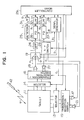
- FIG. 1 there is shown an embodiment of the position detecting apparatus in accordance with the present invention.
- the apparatus is applied to a digitizier for detecting the position pointed in two-dimensional directions, that is, in the X-direction and Y-direction.
- the position to be identified in the position detection section (hereinafter called "tablet") 10 having loop coils arranged on a substrate 75 (Fig. 3) at predetermined intervals in the X- and Y-directions as will be described later, is pointed by a position pointer (hereinafter called "input pen") 11, details of which will be described later.
- input pen position pointer
- Selector means 13 and 14 which may be constituted by known multiplexers and provided for successively switching the X- and Y-direction loop coils, are connected to the tablet 10. These selector means 13 and 14 are respectively connected to transmission/reception switching circuits 15 and 16 for the purposes of transmitting signals to the loop coils and reception signals from the loop coils.
- the receiving sides of the transmission/reception switching circuits 15 and 16 are connected to a reception timing switching means 19 which may be constituted by switches for attaining the timing of reception in the X- and Y-directions through amplifiers 17 and 18.
- the transmission sides of the transmission/reception switching circuits 15 and 16 are connected to an X-Y switching means 23 which may be consti tuted by switches for conducting the switching of transmission in the X- and Y-directions through driving circuits 21 and 22.
- These selector means 13 and 14, transmission/reception switching circuits 15 and 16, reception timing switching means 19 and X-Y switching means 23 constitute a connection switching means.
- the reception timing switching means 19 is connected to a detector 25, a first phase detector (PD) 26 and a second phase detector (PD) 27 through a band-pass filter 24 which constitutes a signal detecting means.
- the first phase detector (PD) 26 and a signal generator 28 are connected to the X-Y switching circuit 23.
- the signal generator 28 is connected also to the reception timing switching circuit 19 so that the reception timing switching means 19 can be controlled so as not to be connected to any one of the amplifiers 17 and 18 when signals from the signal generator 28 are supplied to the transmission/reception switching circuits 15 and 16.
- the operation of the signal generator 28 is controlled by a controller means 29 which may be constituted by a micro-processor.
- the detector 25, the first phase detector 26 and the second phase detector 27 are connected to the controller means 29 through a first low-pass filter (LPF) 31, a second low-pass filter (LPF) 32 and a third low-pass filter (LPF) 33, respectively.
- This controller means 29 is connected to control the switching operations of the selector means 13 and 14, the reception timing switching means 19 and the X-Y switching means 23.
- the X-direction loop coil 41 has a first coil section 43, a second coil section 44, a third coil section 45 and a fourth coil section 46.
- the substantially rectangularly shaped first coil section 43 is composed of a first part 43a extending in the Y-direction from a connection terminal 42, a second part 43b extending substantially perpendicularly to the first part 43a by a length corresponding to the length of a predetermined pitch Px from the ending point of the first part 43a, and a third part 43c extending substantially perpendicularly to the second part 43b from the ending point of the second part 43b so that the direction of an electric current or the direction of magnetic flux can be reversed.
- the second coil section 44 is composed of a first part 44a extending perpendicularly to a connection part 43d extending perpendicularly to the third part 43c of the first coil 43 by a length corresponding to the length of the pitch Px from the ending point thereof, a second part 44b, and a third part 44c.
- the third coil section 45 is composed of a first part 45a provided through a connection part 44d, a second part 45b, and a third part 45c.
- the fourth coil section 46 is composed of a first part 46a provided through a connection part 45d, a second part 46b, and a third part 46c.
- the loop coil 41 further has a fifth coil section 47, a sixth coil section 48 and a seventh coil section 49.
- the fifth coil section 47 is composed of a first part 47a extending perpendicularly to a connection part 46d extending perpendicularly to the third part 46c of the fourth coil section 46 from the ending point thereof so that the first part 47a of the fifth coil section 47 is arranged in parallel to the third part 46a of the fourth part section 46 at a slight distance, a second part 47b extending perpendicularly to the first part 47a by a length corresponding to the length of the pitch Px from the ending point thereof, and a third part 47c extending perpendicularly to the second part 43b from the ending point thereof so that the direction of an electric current or the direction of magnetic flux can be reversed and being arranged in parallel to the third part 45c of the third coil section 45 at a slight distance.
- the six coil section 48 is composed of a first part 48a provided through a connection part 47d, a second part 48b, and a third part 48c.
- the seventh coil section 49 is composed of a first part 49a provided through a connection part 48d, a second part 49b, and a third part 49c.
- the third part 49c of the seventh coil section 49 is connected to a connection terminal 51. Accordingly, a current or flux of the same direction flows in two parts adjacent to each other at a slight distance, for example, in the third parts 43c and 49c of the first and seventh coil sections 43 and 49, so that a high output can be generally attained even if the signal output of the signal generator 28 is low.
- the Y-direction loop coil 52 is distinguished by the dot line from the X-direction loop coil 41.
- the Y-direction loop coil 52 has seven coil sections (a first coil section 53 to a seventh coil section 59) arranged by the same pattern as that of the X-direction loop coil 41.
- the arrangement of the respective coil sections in the Y-direction loop coil 52 is similar to that of the respective coil sections in the X-direction loop coil 41. Details of those coil sections in the Y-direction loop coil 52 will therefore be omitted.
- the Y-direction loop coil 52 is arranged so that the first and third parts of each coil section thereof intersect the first and third parts of each coil section of the X-direction loop coil 41 at an angle of about 90° .
- the Y-direction loop coil 52 is connected between connection terminals 61 and 62.
- the pattern of the loop coils of Fig. 2 is illustrated for the purpose of well understanding the construction of this embodiment.
- eight loop coils are arranged as shown in Fig. 3 to thereby form a tablet 11.
- the X-direction coils are grouped into two coil groups consisting of a first X-direction coil group 67 composed of four loop coils 63, 64, 65 and 66 and a second X-direction coil group 73 composed of four loop coils 68, 69, 71 and 72.
- the reason why each of the coil groups 67 and 73 is composed of four loop coils is to make the resolution high.
- the loop coil 63 is composed of a number, m , of substantially rectangular coil sections 63-1, 63-2, 63-3, ..., and 63-m respectively having long sides which are extended in the Y-direction but reversed in extending direction so that the direction of a current passing therethrough or flux is reversed alternately at every predetermined pitch P1 along the direction of position detection, that is, along the X-direction.
- the loop coils 64, 65 and 66 are composed of m coil sections 64-1, 64-2, 64-3, ..., and 64-m; 65-1, 65-2, 65-3, ..., and 65-m; 66-1, 66-2, 66-3, ..., and 66-m, respectively.
- the coils are numbered from the left of the drawing for the purpose of simplification of description.
- the loop coils 63 and 66 are arranged with displacement from one another by an interval of d1 in the X-direction.
- the loop coil 68 in the second X-direction coil group 73 is composed of a number, (m-1), of substantially rectangular coil sections 68-1, 68-2, 68-3, ..., and 68-(m-1) respectively having long sides which are extended in the X-direction but reversed in extending direction so that the direction of a current passing therethrough or flux is reversed alternately at every predetermined pitch P2 along the X-direction.
- the loop coils 69, 71 and 72 are composed of (m-1) coil sections 69-1, 69-2, 69-3, ..., and 69-(m-1); 71-1, 71-2, 71-3, ..., and 71-(m-1); and 72-1, 72-2, 72-3, ..., and 72-(m-1), respectively.
- the loop coils 68 to 72 are arranged with displacement by an interval of d2 in X-direction.
- the first X-direction coil group 67 and the second X-direction coil group 73 are arranged to overlap each other so that the starting points thereof, that is, one end 63-1a of the coil section 63-1 of the loop coil 63 and one end 68-1a of the coil section 68-1 of the loop coil 68 coincide with each other.
- the coils 63 and 68 are shown separately for the purpose of distinguishing.
- the position detector area is within a range surrounded by the dot-and-dash line designated by the reference numeral 74.
- the loop coils 63 and 72 are used in combination with selec tor elements (not shown) of the selector means 13.
- the loop coils 63 and 68 are used in combination with a first selector element (not shown) of the selector means 13; the loop coils 64 and 69 are used in combination with a second selector element (not shown) of the selector means 13.
- the four pairs of loop coils are successively selected by the selector elements of the selector means 13. Accordingly, the selector elements of the selector means can be simplified in construction.
- the first and second Y-direction coil groups as to the Y-direction of the table 10 are similarly arranged to overlap each other so that the position detection directions thereof intersect each other.
- the X- and Y-direction loop coils are arranged on the substrate 75.
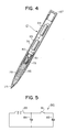
- the input pen 12 has a hollow and tapering casing 76 made of a non-metallic material such as a synthetic resin and shaped like a ball point pen, and a pointing member 77 similar to the core of a ball point pen.
- the pointing member 77 is inserted into the tapering portion of the casing 76 so that one end of the pointing member 77 is movable relative to the top end of the casing 76.
- the pointing member 77 is slidably inserted into a center hole of a ferrite core 78.
- the opposite end of the pointing member 77 touches one end of a coiled spring 79.
- the opposite end of the coiled spring 79 faces a push-button switch 81 at a predetermined distance.
- the switch 81 is mounted to the substrate 82 fixed within the casing 76.
- a tuning circuit 86 is constituted by a coil 83 wound around the ferrite core 78, and capacitors 84 and 85 provided within the casing 76.
- a cap 87 is removably provided in the rear end of the casing 76.
- the tuning circuit 86 is constituted by a coil 83, and capacitors 84 and 85 connected to one end of the coil 83 directly and through the switch 81 respectively.
- the coil 83 is connected in series to the capacitor 84, thus constituting a resonance circuit which is known.
- the reactance and capacitance of the coil 83 and the capacitor 84 are selected so that the tuning circuit can resonate with a predetermined frequency f0.
- the capacitor 85 is connected across the capacitor 84 through the switch 81. The parallel connection of the capacitors serves to reduce or lower the resonance frequency f0 when the switch 81 is turned on.
- the switch 81 When the pointing end of the pointing member 77 is pressed onto the input surface (not shown) of the tablet 11 to be drawn into the casing 76 while the casing 76 is grasped by hand or the like, the switch 81 is pressed by the rear end of the pointing member 77 through the coiled spring 79 so that the switch 81 is turned on. When the pointing member 81 is released, on the contrary, the switch 81 is turned off.
- the controller means 29 controls the signal generator 28, and, at the same time, controls the switching of the loop coils of the tablet 11 through the selector means 13 and 14 in accordance with the flow chart which will be described later. Further, the controller means 29 controls the switching operations of the X-Y switching means 23 and the reception timing switching means 19 in the direction of coordinates detection. In addition, the controller means 29 obtains the coordinates of the position pointed by the input pen 12 by processing signals representing the levels of output voltages from the first, second and third low-pass filters 31, 32 and 33 through A/D conversion and, further, detects the phase of the reception signal to discriminate the state of the switch.
- the selector means 13 successively selects one loop coil from the first and second X-direction coil groups 67 and 73 on the basis of the information given from the controller means 29.
- the selector means 14 successively selects one loop coil from the first and second Y-direction coil groups not shown.
- the transmission/reception switching circuit 15 alternately connects the selected X-direction loop coil to the driving circuit 21 and the amplifier 17.
- the transmission/reception switching circuit 16 alternately connects the selected Y-direction loop coil to the driving circuit 22 and the amplifier 18.
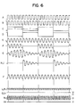
- the signal generator 28 generates a rectangular signal A of a predetermined frequency f0, a signal B having a phase lagged by an angle of 90° from the phase of the rectangular signal A, a transmission/reception switching signal C of a predetermined frequency f k , and a reception timing signal D.
- the rectangular signal A is directly sup plied to the first phase detector 26, converted into a sine-wave signal E by a low-pass filter not shown and then supplied to selected one of the driving circuits 21 and 22 through the X-Y switching means 23.
- the rectangular signal B is supplied to the second phase detector 27.
- the transmission/reception switching signal C is supplied to the transmission/reception switching circuits 15 and 16.
- the reception timing signal D is supplied to the reception timing switching means 19.
- the signal F is supplied to selected one of the X-direction loop coils, for example, the loop coil 63, of the tablet 11 through the selector means 13, so that the loop coil 63 generates an electric wave on the basis of the signal F.
- the afore-mentioned electric wave excites the coil 83 of the input pen 12 so that a voltage G is induced in the tuning circuit 86 in synchronization with the signal F.
- the receiving period begins when the duration of the signal F expires.
- the loop coil 11 is switched to the amplifier 17 side so that the electric wave from the loop coil 11 extinguishes without delay.
- the induced voltage G is progessively attenuated in accordance with the loss in the tuning circuit 86.
- the current flowing in the tuning circuit 86 on the basis of the induced voltage G serves to transmit an electric wave from the coil 83. Because the electric wave is reversely excites the loop coil 63 connected to the amplifier 17, a voltage is induced in the loop coil 63 by the electric wave from the coil 83.
- the induced voltage is supplied to the amplifier through the transmission/reception switching circuit 15 during the receiving period and amplified by the amplifier to form a reception signal H.
- the reception signal H is supplied to the reception timing switching means 19.
- the reception timing switching means 19 receives selected one of the X-direction selector information and the Y-direction selection information. If the X-direction selection information, as well as the reception timing signal D substantially formed by inverting the transmission/reception switching signal C, is supplied to the reception timing switching means 19, a signal I is obtained as the output thereof because the reception signal H is passed when the level of the signal D is high and the reception signal H is not passed when the level of the signal D is low. The signal I is substantially the same as the reception signal H.
- the signal I is supplied to the band-pass filter 24 which is constituted by a ceramic filter having a specific frequency f0.
- the band-pass filter 24 which is constituted by a ceramic filter having a specific frequency f0.
- a signal J (strictly speaking, in the state where several signals I are converged by the band-pass filter 24) having an amplitude corresponding to the energy of a frequency f0 component in the signal I is supplied to the detector 25 and the first and second phase detectors 26 and 27.
- the signal J thus supplied to the detector 25 is detected and rectified so that it is converted into a signal L. Then the signal L is converted, by the first low-pass filter 31 having a sufficiently low cutoff frequency, into a D.C. signal Q having a voltage level (for example, V1) corresponding to about half the amplitude. The thus obtained signal Q is transferred to the controller means 29.
- the voltage level V1 of the signal Q depends on the distance between the input pen 12 and the loop coil 63.
- the loop coil 63 is composed of coil sections 63-1 to 63-m formed substantially over the whole surface of the tablet 11 as described above, the voltage level V1 is, in practice, determined by the position of the input pen 12 relative to the coil sections 63-1 to 63-m. This can be applied to the case where other loop coils 64 to 72 are selected.
- Figs. 7a and 7b show the loop coils 63 to 66 in the first X-direction coil group 67 and the change of detection voltages thereof in the case where the input pen 12 is moved along the X-direction of the tablet 11.
- the loop coils 63 to 66 in the first X-direction coil group 67 are shown; and in Fig. 7b the waveforms of detection voltages corresponding to these loop coils are shown.
- V1 represents the detection voltage of the loop coil 63.
- the voltage V1 is a substantially sine-wave voltage which takes maximum values in the vicinity of the middle of the coil sections 63-1 to 63-m and takes minimum values in the vicinity of the border of the coils.
- V2, V3 and V4 represent the detection voltages of the loop coils 64, 65 and 66, respectively.
- the voltages V2, V3 and V4 change in the same manner as the voltage V1.
- the voltages V1, V2, V3 and V4 are successivelysively delayed by a value corresponding to the distance d1 in the X-direction.
- the portion surrounded by the coil sections 63-1, 64-1,... 66-1 and 63-m, 64-m,... 66-m is designed to locate in the outside of the detection area 74. As these detection voltages depend on the X-direction position of the input pen 12, the levels of voltages detected are not changed even if the input pen 12 is moved in parallel to the Y-direction.
- the distance between adjacent maximum values (or minimum values) of voltage in one loop coil is equal to the pitch P2 of the coils in the loop coil and the phase difference between adjacent voltages in the loop coils 68 to 72 is equal to d2.
- Figs. 8a and 8b show the detection voltages V1 and V5 in one loop coil 63 in the first X-direction coil group 67 and one loop coil 68 in the second X-direction coil group 68.
- the patterns of the loop coils 63 and 68 are shown; and in Fig. 8b the waveforms of the detection voltages corresponding to these loop coils are shown.
- Fig. 8a shows the case where the loop coil 63 has six coil sections and the loop coil 68 has five coil sections, it is to be understood that Fig. 8a shows merely the basic construction of loop coils and that, in fact, each loop coil in the first coil group has a number, m , of coil sections and each loop coil in the second coil group has a number, m-1, of coil sections.
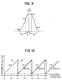
- Fig. 9 is a graph for explaining the calculation of an arbitrary position x0 to be measured.
- the peak point corresponds to the position x0 so that the coordinates d x from the center position x c (the position where the voltages V1 and V2 intersect each other in Fig. 7b) between the voltages V10 and V20 to the peak point is calculated by the following equation (3) using the maximum voltage V20 and the voltages V10 and V30 based on calculus of finite differences.
- d x ⁇
- the equation (3) is generalized as follows.
- V n the maximum voltage
- V n-1 the voltage of a coil in the front of the coil where the voltage V n is detected
- V n+1 the voltage of a coil in the rear of the coil where the voltage V n is detected.
- the coordinates d x is a coordinates value based on the position where the voltages V1 and V2 intersect each other, the coordinates value is reduced by the distance d1 compared with the value of the coordinates ⁇ x.
- the coordinates d x takes a value based on the position where the voltages V4 and V1 intersect each other
- the coordinates d x takes a value based on the position where the voltages V1 and V2 intersect each other or based on the position where the voltages V2 and V3 intersect each other or based on the position where the voltages V3 and V4 intersect each other.
- the coordinates ⁇ x can be obtained as follows.
- ⁇ x d x (4-1)
- the coordinates ⁇ x can be obtained as follows.
- ⁇ x d x + d1 (4-2)
- the coordinates ⁇ x can be obtained as follows.
- ⁇ x d x + 2d1 (4-3)
- the coordinates ⁇ x can be obtained as follows.
- ⁇ x d x + 3d1 (4-4)
- the coordinates ⁇ x′ of the position x0 within the distance of the pitch P2 from a predetermined position for example, a position where the voltage V8 detected from the coil 72 and the voltage V5 detected from the coil 68 intersect each other, can be obtained on the basis of the voltages detected from the loop coils of the second X-direction coil group in the same manner as described above.
- Fig. 10 shows the relation between the coordinates ⁇ x and ⁇ x′ obtained by the first and second X-direction coil groups 67 and 73 and the X-direction real position.
- the solid line 91 shows the coordinates ⁇ x
- the broken line 92 shows the coordinates ⁇ x′.
- the difference between the coordinates ⁇ x and ⁇ x′ is based on the difference between the pitches P1 and P2 in the first and second X-direction coil groups 67 and 73.
- a difference proportional to integral multiples of the difference between the pitches P1 and P2 is produced corresponding to the position of the input pen 12 which exists in any one of coils in the coil group 67.
- the X-direction real position x0 where the input pen 12 exists can be obtained conversely on the basis of this difference.
- the position coordinates x0 can be obtained by the following equation (6).
- x0 KP1 + ⁇ x (6)
- the origin in the X-direction is the position where the voltages V4 and V1 intersect each other. (On the tablet 11, the origin is the position which is less by d1/2 than the middle position of the coil section 63-1).
- the Y-direction position pointed by the input pen 12 can be also obtained in the same manner as described above.
- the first and second phase detectors 26 and 27 receive, as the detecting signals, rectangular signals A and B as shown in Fig. 6. If the phase of the signal J coincides with the phase of the rectangular signal A, the first phase detector 26 produces a signal R1 (being substantially the same as the signal L) which is formed by inverting the signal J to the positive side. The second phase detector 27 produces a signal R2 having a symmetrical waveform with respect to the positive and negative sides.
- the signal R1 is converted, by the second low-pass filter 32, into a D.C. signal U1 (being substantially the same as the signal Q) having a voltage level V1 corresponding to about half the amplitude of the signal J, so that the thus obtained signal U1 is transferred to the controller means 29.
- the signal R2 is also converted into a D.C. signal U2 by the similar low-pass filter 11, so that the thus obtained signal U2 is transferred to the controller means 29. Because the positive-side component of the signals R2 in the second phase detector 27 is the same as the negative-side component thereof, the output voltage level of the low-pass filter 44 becomes zero [V].
- the output signals U1 and U2 of the second and third low-pass filters 32 and 33 are converted into corresponding digital signals and are subjected to arithmetic operation in accordance with the following equation (6) to obtain the phase difference ⁇ between the signals supplied to the first and second phase detectors 26 and 27, that is, the signal J and the rectangular signal A.
- ⁇ -tan ⁇ 1(V q /V p ) (6)
- V p represents a digital value corresponding to the output of the second low-pass filter 32
- V q represents a digital value corresponding to the output of the third low-pass filter 33.
- the phase of the signal J varies corresponding to the tuned frequency in the tuning circuit 86 of the input pen 12.
- a voltage of the frequency f0 is induced both during the signal transmission period and during the signal receiving period.
- an induced current flows in synchronism with the voltage, so that the frequency and phase of the reception signal H (or I) coincide with those of the rectangular signal A, and, consequently, the phase of the signal J coincides with the phase of the rectangular signal A.
- the tuned frequency in the tuning circuit 86 does not coincide with the predetermined frequency f0 and has a frequency f1 slightly lower than the frequency f0, a voltage of the frequency f0 is induced in the tuning circuit 86 in the transmission period. At this time, an induced current having a lagging phase flows in the tuning circuit 83. In the received period, a voltage having a frequency f1 is induced and a current induced in synchronism with the voltage flows in the tuning circuit 96, so that the frequency of the reception signal H (or I) is slightly lower than the frequency of the rectangular signal A as well as the phase of the signal H is slightly lagged.
- the band-pass filter 24 serves to pass only the frequency f0 as described above, the shift of frequency of the input signal into a lower side is sent out as the lagging of phase so that the phase of the signal J more lags than the reception signal H (or I).
- the tuned frequency in the tuning circuit 86 is a frequency f2 slightly higher than the predetermined frequency f0
- an induced current having a leading phase flows in the tuning circuit 86 while a voltage having the frequency f0 is induced in the tuning circuit 86 in the transmission period.
- a voltage substantially having the frequency f2 is induced and an induced current flows in synchronism with the voltage in the tuning circuit 86, so that the frequency of the reception signal H (or I) is slight higher than the frequency of the rectangular signal A as well as the phase of the signal H leads slightly.
- the band-pass filter 24 the shift of frequency of the input signal toward a higher frequency is sent out as a leading phase, so that the phase of the signal J more leads than the reception signal H (or I).
- the tuned frequency in the tuning circuit 86 varies according to the ON/OFF state of the switch 81 of the input pen, so that the phase difference ⁇ obtained by the equation (6) varies according to the ON/OFF state of the switch 81. Accordingly, the ON/OFF state of the switch 81 can be detected by the change in the phase difference ⁇ . The state of ON (or OFF) of the switch 81 thus detected is used as information for designating a value actually to be inputted, of the values of coordinates of the position pointed by the input pen 12.
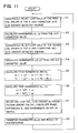
- controller means 29 In the following, the operation of the controller means 29 is described with reference to the flow chart shown in Fig. 11.
- the position detecting operation is commenced as the power supply is turned on the supply electric power to the whole apparatus.
- the controller means 29 supplies both the X-Y switching means 23 and the receiving timing switching means 19 with information for selecting the X-direction.
- the controller means 29 supplies the selection circuit 13 with instructions for enabling the selection circuit 13 to select the first loop coil 63 out of the loop coils 63 to 66 in the first X-direction coil group 67 of the tablet 11, thereby connecting the loop coil 63 to the transmission/receiving switching circuit 15.
- the transmission/receiving switching circuit 15 connects the loop coil 63 alternately to the driving circuit 21 and the amplifier 17 in accordance with the transmission/receiving switching signal C.
- the driving circuit 21 sends 16 sine-wave signals of a frequency f0 to the loop coil 63.
- Fig.6 five ones of those 16 signals are shown for the purpose of explanation.
- the switching between transmission and reception is repeated seven times for each loop coil, for example, for the loop coil 63.
- the total period of those seven cycles of switching between transmission and reception corresponds to the period over which each loop coil is selected.
- the induced voltage is obtained at the output of the amplifier 17 in each of the seven signal-reception periods for every loop coil.
- the induced voltages thus obtained in the seven signal-reception periods for every loop coil are transferred to the band-pass filter 24 through the reception timing switching means 19 as explained before and are averaged by the band-pass filter 24.
- the averaged voltage is delivered to the controller means 29 through the first, second and third low-pass filters 31, 32 and 33.
- the output signal of the low-pass filter 31 is processed by the controller means 29 so as to be converted into the detection voltage V11 corresponding to the distance between the input pen 12 and the loop coil 63.
- the detection voltage V11 is stored temporally.
- the controller means 29 supplies the selection circuit 13 with instructions to make the selection circuit 13 to select the second loop coil 64 so that the loop coil 64 is connected to the transmission/reception switching circuit 15. Consequently, a detection voltage V12 proportional to the distance between the input pen 12 and the loop coil 64 is obtained and stored.
- the foregoing operation is conducted for all the remaining loop coils 65 and 66 by successively connecting the loop coils to the transmission/reception switching circuit 15, whereby the respective detection voltages V11 to V14 corresponding to the X-direction distances between the input pen and the respective loop coils are obtained and stored.
- the controller means 29 supplies both the X-Y switching means 23 and the reception timing switching means 19 with information for selecting the Y-direction.
- the switching between the selection circuit 14 and the transmission/reception switching circuit 16 is conducted, so that detection voltages corresponding to the distances between the input pen and the respective loop coils of the first Y-direction coil group are obtained by A/D conversion of the output of the low-pass filter when electric waves are transmitted and received, and the detec tion voltages are stored temporally (Step S1).
- the controller means 29 executes an arithmetic operation in accordance with the equation (3)′ and selected one of the equations (4-1) to (4-4) on the basis of the stored voltage values, to thereby calculate and store the coordinates ⁇ x and ⁇ y on the basis of the first X- and Y-direction coil groups (Step S2).
- the controller means 29 delivers to the X-Y switching means 23 and the reception timing switching means 19 information for selecting X-direction, so that the switching between the selection circuit and the transmission/reception switching circuit 15 is conducted in the same manner as described above.
- detection voltages corresponding to the distances between the input pen and the respective loop coils 68 to 72 of the second X-direction coil group 73 are obtained by A/D conversion of the output of the first low-pass filter 31 when electric waves are transmitted and received, and the detection voltages are stored temporally.
- the controller means 29 supplies both the X-Y switching means 23 and the reception timing switching means 19 with information for selecting the Y-direction.
- Step S3 the switching between the selection circuit 14 and the transmission/reception switching circuit 16 is conducted, so that detection voltages corresponding to the distances between the input pen 12 and the respective loop coils of the second Y-direction coil group are obtained by A/D conversion of the output of the first low-pass filter 31 when electric waves are transmitted and received, and the detection voltages are stored temporarily (Step S3).
- the controller means 29 executes an arithmetic operation in accordance with the equation (3)′ and selected one of the equations (4-1) to (4-4) on the basis of the stored voltage values, to thereby calculate and store the coordinates ⁇ x′ and ⁇ y′ on the basis of the second X- and Y-direction coil groups (Step S4).
- controller means 29 executes an arithmetic operation in accordance with the equation (5) on the basis of the stored coordinates values ⁇ x, ⁇ x′, ⁇ y and ⁇ y′, to thereby calculate the pitch numbers Kx and Ky (Step S5).
- the controller means 29 executes an arithmetic operation in accordance with the equation (6) on the basis of the pitch numbers, the pitch P1 and the coordinates ⁇ x and ⁇ y, to thereby calculate the true coordinates X0 and y0 (Step S6).
- the controller means 29 supplies instructions to the selection circuit 13 (or 14) to make the selection circuit 13 to select arbitrary one of the X-direction loop coils 63 to 72 (or Y-direction loop coils), so that the transmission and reception of electric waves are repeated several times, for example, seven times. Consequently, the output values obtained from the second and third low-pass filters 32 and 33 are converted into corresponding digital signals, so that the phase difference ⁇ is calculated in the same manner as described above to thereby discriminate the ON/OFF state of the switch 81 (Step S7).
- the coordinates of all the positions pointed by the input pen 12 are transferred to the computer or the like. If the switch 81 is turned on in this condition, the information for discrimination of the ON state of the switch 81 is transferred to the computer or the like so that the computer can recognize the coordinates value at this point of time as a coordinates value to be inputted.
- each of the loop coils is constituted by rectangular coil sections formed in a manner so that a conductor is reversely turned again and again at predetermined pitches from one-end side toward the opposite-end side to form part of the coil sections and then further reversely turned again and again at the predetermined pitches from the opposite-end side to the one-end side to form the remainder coil sections as illustrated in Fig. 2.
- the pattern of the loop coils is not limited to the specific embodiment but may be formed, for example, in such a manner as shown in Fig. 12.
- the coil 93 in the first X-direction coil group may be constructed in a manner so that a conductor is reversely turned again and again at predetermined pitches Px from the one-end side to the opposite-end side to form given number of substantially rectangular coil sections and then the end of the conductor is connected directly to the connection terminal after the coil section reaches the opposite-end side.
- the coil 94 in the first Y-direction coil group may be constructed in a manner so that a conductor is reversely turned again and again at predetermined pitches Py from the one-end side to the opposite-end side to form given number of substantially rectangular coil sections and then the end of the conductor is connected directly to the connection terminal after the coil section reaches the opposite-end side.
- the coils in the second X- and Y-direction coil groups may be formed substantially rectangularly so that the direction of current or flux is inverted alternately at every predetermined pitch Px′, Py′ in the X- and Y-directions as explained before.
- the coil 95 may be provided doubly for the purpose of increasing the output electric wave energy in the detection section in spite of the low level output of the signal generator 28, so that electric wave can be securely generated from the input pen 12 thus to attain reliable position detection.
- the double structure may be formed by overlapping coils so that the coils displace horizontally from each other at a slight distance. It is a matter of course that the coil may have any suitable multi-layer structure of three layers or more.
- the transmission/reception switching circuits 15 and 16 are provided for the purpose of transmitting signals to loop coils and receiving signals from the input pen 12.
- the loop coils are used as an antenna for transmission as well as for reception.
- the aforementioned loop coils 63 to 72 may be used as an antenna only for transmitting signals from the signal generator 28 while a further combination of loop coils hav ing the same pattern of the loop coils 63 to 72 are provided on the loop coils 63 to 72 through insulators as an antenna only for reception.
- Those coils for transmission and those coils for reception may be vertically put one on the other, or alternatively they may be horizontally slightly displaced from each other.
- the transmission/reception switching circuits 15 and 16 can be omitted to simplify the apparatus in construction.
- each of the X- and Y-direction first and second coil groups is constructed by four loop coils for the purpose of increasing the resolution of the apparatus, it is a matter of course that each of the coil groups may be constructed by five or more loop coils for the purpose of further increasing the resolution. If such high resolution is not required, each of the first and second coil groups may be constructed by two loop coils. In this case, the position pointed by the input pen 12 is identified on the basis of two different detection voltages.
- the position detecting apparatus may be constructed in a manner so that a plane-type display unit such as a liquid-crystal display unit is put on the tablet to indicate the input result on the display unit on real time and in combination of input and output. Further, the position detecting apparatus can be used as a terminal device for transmitting information such as handwriting letters/characters between users of the apparatus through modems connected to computers and telephone circuits. Further, the input results can be produced as hard copies through printers.
Abstract
Description
- The present invention relates to a position detecting apparatus for detecting the position of a position detection section pointed by a cordless position pointer and, more particularly, it relates to a position detecting apparatus including a position pointer provided with a tuning circuit and a position detection section provided with loop coils for transmitting electric wave by which a designated position of the position detection section can be detected by using the reflection of the electric wave from the position pointer.
- A position detecting apparatus having a position detection section provided with a large number of signal lines arrayed at predetermined intervals both in the X-direction and in the Y-direction, and a position pointer for pointing a suitable measurement position of the position detection section, in which the position pointed by the position pointer is identified by catching the position as the X-Y co-ordinates by driving the X-direction and Y-direction signal lines successively, has been widely used as a graphic/character input apparatus generally called "tablet" or "digitizer".
- As one of the apparatus of the type described above, a graphic information input apparatus is disclosed in Japanese Patent Unexamined Publication No. 58-176933 laid open on May 10, 1983. The graphic information input apparatus has a position detection section in which a plurality of driving lines are arranged at intervals in the X-direction and a plurality of detecting lines are arranged at intervals in the Y-direction and perpendicularly to the driving lines, and a position pointer having a magnetic material such as ferrite. In the disclosed apparatus, the driving lines are successively supplied with an electric current and the detecting lines are accessed sequentially so that the position pointed by the position pointer is identified by the position of the detecting line on which the highest voltage is induced.
- The disclosed apparatus has an advantage in that the position pointer is easy to handle, because the position pointer can be provided as a cordless device having nothing but a function of transmitting a magnetic signal. The position of the position detection section which can be detected is a rectangular position surrounded by the driving and detecting lines. Accordingly, the resolution of the coordinates position is determined by the pitch of the lines. A higher resolution would be obtained by reducing the pitch of the lines, but such a reduced pitch will undesirably impair the signal-to-noise ratio, S/N, of the detection signal as well as the stability of detection performance, so that improvement in the resolution is limited by itself. In addition, it is rather difficult to detect the position right above each of intersections of the driving lines and the detecting lines. Furthermore, the disclosed apparatus has also a problem in that it is difficult to detect the position if the position pointer cannot be placed in the very close proximity of each driving line.
- Therefore, the assignee of the present application has already proposed a position detecting apparatus as disclosed in European Patent Application Publication No. 0 259 894 dated March 16, 1988. The proposed apparatus has a position detection section in which a plurality of loop coils having rectangular patterns are arranged at predetermined intervals both in the X-direction and in the Y-direction, and a position pointer having a tuning circuit including a coil and a capacitor and adapted to resonate with electric wave produced by the loop coils.
- The proposed apparatus further has a selection circuit for successively selecting the loop coils one by one, a transmission circuit for generating an A.C. signal of a predetermined frequency to be supplied to the loop coils, a receiving circuit for detecting an induced voltage of a frequency substantially the same as that of the A.C. signal of the transmission circuit out of various voltages induced in the loop coils, a connection switching circuit for connecting the selected loop coil to the transmission circuit and the receiving circuit, and a controller means for determining the position pointed by the position pointer on the basis of the levels of voltages induced in the loop coils.
- In the proposed position detecting apparatus, a loop coil is selected out of a plurality of loop coils by the selection circuit and the transmission circuit is connected to this selected loop coil by means of the connection switching circuit so that an A.C. current is supplied to the loop coil, by which an electric wave is generated by the loop coil. The electric wave thus generated excites the coil in the position pointer which points a position on the position detection area, so that a voltage is induced in the coil in synchronization with the A.C. current. If the connection switching circuit is changed over from the transmission circuit side to the receiving circuit side, the electric wave from the selected loop coil will stop. Thereafter, the receiving circuit is connected to the loop coil selected by the connection switching circuit and, at the same time, the supply of the A.C. current is ceased so that the electric wave is extinguished. Meanwhile, a current corresponding to the induced voltage flows in the tuning circuit in the position pointer, so that the coil in the tuning circuit generates an electric wave. This electric wave reversely excites the loop coil which has been selected and connected to the receiving circuit, so that a voltage is induced in the the loop coil. The aforementioned change-over between the electric-wave transmission and reception is conducted successively on all the loop coils. Because this change-over between the electric-wave transmission and reception relies upon resonance between each loop coil and the coil in the position pointer, the level of the voltage induced in the loop coil has such a dependency on the distance between the loop coil and the coil of the position pointer that the level of the induced voltage is highest in the loop coil which is closest to the present position pointed by the position pointer and is gradually decreased as the distance between the loop coil and the coil of the position detector is increased. The levels of voltages induced in these loop coils are processed by the controller means so that the coordinates of the position pointed by the position pointer can be identified by the position of the loop coil which exhibits the highest level of the induced voltage among the loop coils. Because the position pointed by the position pointer is determined by the induced voltage thus detected, the precision of position detection can be increased by enhancing the precision of arithmetic operation of the controller means on the levels of induced voltages in the plurality of loop coils. Thus, a high-resolution position detecting apparatus can be provided.
- An object of the present invention is to provide a position detecting apparatus incorporating a cordless position pointer which is not connected to any part of the stationary portion of the apparatus, thus facilitating the handling while attaining a high degree of precision in position detection and, at the same time, capable of detecting two-dimensional coordinates value of the pointed position in a rectangular coordinate system.
- Another object of the invention is to provide a position detecting apparatus incorporating a position detection section having a plurality of loop coils which are respectively composed of a plurality of coils and are arranged at predetermined intervals, thus attaining a high degree of resolution.
- A further object of the invention is to provide a position detecting apparatus incorporating a few number of switching means for selecting the loop coils, thus attaining a reduction of the number of parts while attaining reduction of the weight of the apparatus.
- To attain the above objects, according to the present invention, there is provided a position detecting apparatus which comprises: a position detection section having first and second coil groups provided on a substrate, each of the coil groups being composed of a plurality of loop coils; a position pointer having a tuning circuit including at least one coil and one capacitor and having a predeter mined frequency as a tuning frequency; selection means for successively selecting the loop coils of each of the first and second coil groups of the position detection section one by one; signal generation means for applying an A.C. signal of the predetermined frequency to the loop coils; signal detection means for detecting the A.C. signal of the predetermined frequency from the loop coils; and controller means for identifying a position pointed by the position pointer on the basis of the A.C. signal detected by the signal detection means from each of the loop coils of each of the first and second coil groups. Each of the loop coils of each of the first and second coil groups is composed of a plurality of substantially rectangular coil sections formed continuously. The loop coils of the first coil group are arranged with displacement from one another by a predetermined pitch d₁ along the direction of position detection, and each of the rectangular coil sections of each of the loop coils of the first coil group is composed of a first part extending substantially perpendicularly to the direction of position detection, a second part extending substantially in parallel to the first part at an interval of predetermined pitch P1, and a third part for connection between the forward end of the first part and the starting point of the second part. Similarly, the loop coils of the second coil group are arranged with displacement from one another by a predetermined pitch d₂ along the direction of position detection, and each of the rectangular coil sections of each of the loop coils of the second coil group is composed of a fourth part extending substantially perpendicularly to the direction of position detection, a fifth part extending substantially in parallel to the fourth part at an interval of predetermined pitch P2, and a sixth part for connection between the forward end of the fourth part and the starting point of the fifth part.
- As described above, the position pointer requires nothing but a tuning circuit composed of a coil and a capacitor, so that the position pointer can be provided as a cordless device. Further, the position pointer does not require any magnet and any electric source. The loop coils of the position detection section are grouped into the first and second coil groups each composed of a plurality of coil sections and arranged to cover substantially the whole surface of the position detection section. Accordingly, the loop coils of this position detection section can be remarkably reduced in number compared with those of the conventional position detection section. Accordingly, the number of selector elements in the selection means can be reduced remarkably. Further, each of the first and second coil groups is composed of a plurality of loop coil sections which have the same form and are arranged with displacement by a pitch d₁ and by a pitch d₂, respectively, so that the levels of voltages coinciding with each other can be detected. Accordingly, as the number of detected voltages increase, the precision of position detection in the position detecting apparatus increases, and, at the same time, the resolution of the apparatus increases.
- Other features and advantages of the present invention will be apparent from the following description taken in connection with the accompanying drawings, in which.
- Fig. 1 is a block diagram showing the basic con struction of an embodiment of the position detecting apparatus according to the present invention;
- Fig. 2 is a diagram for explaining the basic pattern of X- and Y-direction loop coils which form a tablet;
- Fig. 3 is a partly cutaway diagram of the loop coils in the X-direction of the tablet;
- Fig. 4 is a plan view partly in section, showing the internal construction of the input pen;
- Fig. 5 is a circuit diagram showing the electrical construction of the input pen;
- Fig. 6 is a waveform chart showing waveforms of signals obtained in various portions of the embodiment of Fig. 1;
- Figs. 7a and 7b are views showing the respective loop coils in the first coil group and the change of voltages detected from the loop coils, in which Fig. 7a shows the pattern of loop coils in the first coil group and Fig. 7b shows the waveforms of voltages detected corresponding to these patterns;
- Figs. 8a and 8b are views showing loop coils picked up by each one out of the first and second coil groups and the change of voltages detected from the loop coils, in which Fig. 8a shows the patterns of the loop coils, and Fig. 8b shows the waveforms of voltages detected corresponding to these patterns;
- Fig. 9 is a waveform graph for explaining the calculation of a position to be measured;
- Fig. 10 is a waveform graph showing the relation between the coordinates Δx and Δx′ and the true position;
- Fig. 11 is a flow chart showing the operation of the controller means;
- Fig. 12 is a diagram for explaining another embodiment which is different in the form of loop coils; and
- Fig. 13 is a diagram for explaining a further embodiment which is different in the form of loop coils.
- Referring to Fig. 1, there is shown an embodiment of the position detecting apparatus in accordance with the present invention. In this embodiment the apparatus is applied to a digitizier for detecting the position pointed in two-dimensional directions, that is, in the X-direction and Y-direction. The position to be identified in the position detection section (hereinafter called "tablet") 10 having loop coils arranged on a substrate 75 (Fig. 3) at predetermined intervals in the X- and Y-directions as will be described later, is pointed by a position pointer (hereinafter called "input pen") 11, details of which will be described later. Selector means 13 and 14 which may be constituted by known multiplexers and provided for successively switching the X- and Y-direction loop coils, are connected to the tablet 10. These selector means 13 and 14 are respectively connected to transmission/
reception switching circuits reception switching circuits reception switching circuits circuits reception switching circuits - The reception timing switching means 19 is connected to a
detector 25, a first phase detector (PD) 26 and a second phase detector (PD) 27 through a band-pass filter 24 which constitutes a signal detecting means. The first phase detector (PD) 26 and asignal generator 28 are connected to theX-Y switching circuit 23. Thesignal generator 28 is connected also to the receptiontiming switching circuit 19 so that the reception timing switching means 19 can be controlled so as not to be connected to any one of the amplifiers 17 and 18 when signals from thesignal generator 28 are supplied to the transmission/reception switching circuits signal generator 28 is controlled by a controller means 29 which may be constituted by a micro-processor. Thedetector 25, thefirst phase detector 26 and thesecond phase detector 27 are connected to the controller means 29 through a first low-pass filter (LPF) 31, a second low-pass filter (LPF) 32 and a third low-pass filter (LPF) 33, respectively. This controller means 29 is connected to control the switching operations of the selector means 13 and 14, the reception timing switching means 19 and the X-Y switching means 23. - Referring to Fig. 2, there are shown one X-direction loop coil and one Y-direction loop coil which are picked up from the plurality of X- and Y-direction loop coils in the tablet 10, for description of the basic pattern of the loop coils. The
X-direction loop coil 41 has afirst coil section 43, asecond coil section 44, athird coil section 45 and afourth coil section 46. The substantially rectangularly shapedfirst coil section 43 is composed of afirst part 43a extending in the Y-direction from aconnection terminal 42, asecond part 43b extending substantially perpendicularly to thefirst part 43a by a length corresponding to the length of a predetermined pitch Px from the ending point of thefirst part 43a, and athird part 43c extending substantially perpendicularly to thesecond part 43b from the ending point of thesecond part 43b so that the direction of an electric current or the direction of magnetic flux can be reversed. Similarly to this, thesecond coil section 44 is composed of a first part 44a extending perpendicularly to aconnection part 43d extending perpendicularly to thethird part 43c of thefirst coil 43 by a length corresponding to the length of the pitch Px from the ending point thereof, asecond part 44b, and athird part 44c. Similarly, thethird coil section 45 is composed of afirst part 45a provided through aconnection part 44d, asecond part 45b, and athird part 45c. Similarly, thefourth coil section 46 is composed of afirst part 46a provided through aconnection part 45d, asecond part 46b, and athird part 46c. Theloop coil 41 further has afifth coil section 47, asixth coil section 48 and aseventh coil section 49. Thefifth coil section 47 is composed of afirst part 47a extending perpendicularly to aconnection part 46d extending perpendicularly to thethird part 46c of thefourth coil section 46 from the ending point thereof so that thefirst part 47a of thefifth coil section 47 is arranged in parallel to thethird part 46a of thefourth part section 46 at a slight distance, asecond part 47b extending perpendicularly to thefirst part 47a by a length corresponding to the length of the pitch Px from the ending point thereof, and athird part 47c extending perpendicularly to thesecond part 43b from the ending point thereof so that the direction of an electric current or the direction of magnetic flux can be reversed and being arranged in parallel to thethird part 45c of thethird coil section 45 at a slight distance. Similarly, the sixcoil section 48 is composed of afirst part 48a provided through aconnection part 47d, asecond part 48b, and athird part 48c. Similarly, theseventh coil section 49 is composed of afirst part 49a provided through aconnection part 48d, asecond part 49b, and a third part 49c. The third part 49c of theseventh coil section 49 is connected to aconnection terminal 51. Accordingly, a current or flux of the same direction flows in two parts adjacent to each other at a slight distance, for example, in thethird parts 43c and 49c of the first andseventh coil sections signal generator 28 is low. - In Fig. 2, the Y-
direction loop coil 52 is distinguished by the dot line from theX-direction loop coil 41. The Y-direction loop coil 52 has seven coil sections (afirst coil section 53 to a seventh coil section 59) arranged by the same pattern as that of theX-direction loop coil 41. The arrangement of the respective coil sections in the Y-direction loop coil 52 is similar to that of the respective coil sections in theX-direction loop coil 41. Details of those coil sections in the Y-direction loop coil 52 will therefore be omitted. The Y-direction loop coil 52 is arranged so that the first and third parts of each coil section thereof intersect the first and third parts of each coil section of theX-direction loop coil 41 at an angle of about 90° . The Y-direction loop coil 52 is connected between connection terminals 61 and 62. - The pattern of the loop coils of Fig. 2 is illustrated for the purpose of well understanding the construction of this embodiment. In this embodiment, eight loop coils are arranged as shown in Fig. 3 to thereby form a tablet 11. For simplification, only the coils in the X-direction are shown in Fig. 3. The X-direction coils are grouped into two coil groups consisting of a first
X-direction coil group 67 composed of fourloop coils X-direction coil group 73 composed of fourloop coils coil groups - The
loop coil 63 is composed of a number, m, of substantially rectangular coil sections 63-1, 63-2, 63-3, ..., and 63-m respectively having long sides which are extended in the Y-direction but reversed in extending direction so that the direction of a current passing therethrough or flux is reversed alternately at every predetermined pitch P1 along the direction of position detection, that is, along the X-direction. Similarly, the loop coils 64, 65 and 66 are composed of m coil sections 64-1, 64-2, 64-3, ..., and 64-m; 65-1, 65-2, 65-3, ..., and 65-m; 66-1, 66-2, 66-3, ..., and 66-m, respectively. In Fig. 3 and the following description, the coils are numbered from the left of the drawing for the purpose of simplification of description. Further, the loop coils 63 and 66 are arranged with displacement from one another by an interval of d₁ in the X-direction. - On the other hand, the
loop coil 68 in the secondX-direction coil group 73 is composed of a number, (m-1), of substantially rectangular coil sections 68-1, 68-2, 68-3, ..., and 68-(m-1) respectively having long sides which are extended in the X-direction but reversed in extending direction so that the direction of a current passing therethrough or flux is reversed alternately at every predetermined pitch P2 along the X-direction. - Similarly, the loop coils 69, 71 and 72 are composed of (m-1) coil sections 69-1, 69-2, 69-3, ..., and 69-(m-1); 71-1, 71-2, 71-3, ..., and 71-(m-1); and 72-1, 72-2, 72-3, ..., and 72-(m-1), respectively. The loop coils 68 to 72 are arranged with displacement by an interval of d₂ in X-direction.
- In this embodiment the first
X-direction coil group 67 and the secondX-direction coil group 73 are arranged to overlap each other so that the starting points thereof, that is, one end 63-1a of the coil section 63-1 of theloop coil 63 and one end 68-1a of the coil section 68-1 of theloop coil 68 coincide with each other. However, such coincidence is not always required. In the drawing, thecoils reference numeral 74. The loop coils 63 and 72 are used in combination with selec tor elements (not shown) of the selector means 13. For example, the loop coils 63 and 68 are used in combination with a first selector element (not shown) of the selector means 13; the loop coils 64 and 69 are used in combination with a second selector element (not shown) of the selector means 13. As described above, the four pairs of loop coils are successively selected by the selector elements of the selector means 13. Accordingly, the selector elements of the selector means can be simplified in construction. - Though not shown, the first and second Y-direction coil groups as to the Y-direction of the table 10 are similarly arranged to overlap each other so that the position detection directions thereof intersect each other. The X- and Y-direction loop coils are arranged on the
substrate 75. - Referring to Fig. 4, the detailed construction of the
input pen 12 is shown. Theinput pen 12 has a hollow and taperingcasing 76 made of a non-metallic material such as a synthetic resin and shaped like a ball point pen, and a pointingmember 77 similar to the core of a ball point pen. The pointingmember 77 is inserted into the tapering portion of thecasing 76 so that one end of the pointingmember 77 is movable relative to the top end of thecasing 76. The pointingmember 77 is slidably inserted into a center hole of aferrite core 78. The opposite end of the pointingmember 77 touches one end of acoiled spring 79. The opposite end of the coiledspring 79 faces a push-button switch 81 at a predetermined distance. Theswitch 81 is mounted to thesubstrate 82 fixed within thecasing 76. As shown in Fig. 5, atuning circuit 86 is constituted by acoil 83 wound around theferrite core 78, andcapacitors casing 76. Acap 87 is removably provided in the rear end of thecasing 76. - In short, as shown in Fig. 5, the
tuning circuit 86 is constituted by acoil 83, andcapacitors coil 83 directly and through theswitch 81 respectively. As will be understood also from Fig. 5, thecoil 83 is connected in series to thecapacitor 84, thus constituting a resonance circuit which is known. The reactance and capacitance of thecoil 83 and thecapacitor 84 are selected so that the tuning circuit can resonate with a predetermined frequency f₀. On the other hand, thecapacitor 85 is connected across thecapacitor 84 through theswitch 81. The parallel connection of the capacitors serves to reduce or lower the resonance frequency f₀ when theswitch 81 is turned on. When the pointing end of the pointingmember 77 is pressed onto the input surface (not shown) of the tablet 11 to be drawn into thecasing 76 while thecasing 76 is grasped by hand or the like, theswitch 81 is pressed by the rear end of the pointingmember 77 through thecoiled spring 79 so that theswitch 81 is turned on. When the pointingmember 81 is released, on the contrary, theswitch 81 is turned off. - The operation of this embodiment will be described more in detail hereunder. The description will be commenced first in regard to the exchange of electric waves between the tablet 11 and the
input pen 12, as well as signals obtained as a result of the exchange of the electric waves, with reference to Fig. 6. - The controller means 29 controls the
signal generator 28, and, at the same time, controls the switching of the loop coils of the tablet 11 through the selector means 13 and 14 in accordance with the flow chart which will be described later. Further, the controller means 29 controls the switching operations of the X-Y switching means 23 and the reception timing switching means 19 in the direction of coordinates detection. In addition, the controller means 29 obtains the coordinates of the position pointed by theinput pen 12 by processing signals representing the levels of output voltages from the first, second and third low-pass filters - The selector means 13 successively selects one loop coil from the first and second
X-direction coil groups reception switching circuit 15 alternately connects the selected X-direction loop coil to the drivingcircuit 21 and the amplifier 17. On the other hand, the transmission/reception switching circuit 16 alternately connects the selected Y-direction loop coil to the drivingcircuit 22 and the amplifier 18. - The
signal generator 28 generates a rectangular signal A of a predetermined frequency f₀, a signal B having a phase lagged by an angle of 90° from the phase of the rectangular signal A, a transmission/reception switching signal C of a predetermined frequency fk, and a reception timing signal D. The rectangular signal A is directly sup plied to thefirst phase detector 26, converted into a sine-wave signal E by a low-pass filter not shown and then supplied to selected one of the drivingcircuits second phase detector 27. The transmission/reception switching signal C is supplied to the transmission/reception switching circuits - If information for X-direction selection is given to the X-Y switching means 23 and the reception timing switching means 19 from the controller means 29, the sine-wave signal E is supplied to the driving
circuit 21, converted into a balanced signal and then supplied to the transmission/reception switching circuit 15. Because the transmission/reception switching circuit 15 connects selected one of the drivingcircuit 21 and the amplifier 17 on the basis of the transmission/reception switching signal C, the signal supplied from the transmission/reception switching circuit 15 to the selector means 13 is represented by an intermittent signal F having a frequency f₀ and being supplied to the selector means 13 at every other period T (=1/2fk). - The signal F is supplied to selected one of the X-direction loop coils, for example, the
loop coil 63, of the tablet 11 through the selector means 13, so that theloop coil 63 generates an electric wave on the basis of the signal F. - If the
input pen 12 is erected on the tablet 11 or in other words if theinput pen 12 is now in use, the afore-mentioned electric wave excites thecoil 83 of theinput pen 12 so that a voltage G is induced in thetuning circuit 86 in synchronization with the signal F. - The receiving period begins when the duration of the signal F expires. As the receiving period starts, the loop coil 11 is switched to the amplifier 17 side so that the electric wave from the loop coil 11 extinguishes without delay. However, the induced voltage G is progessively attenuated in accordance with the loss in the
tuning circuit 86. - On the other hand, the current flowing in the
tuning circuit 86 on the basis of the induced voltage G serves to transmit an electric wave from thecoil 83. Because the electric wave is reversely excites theloop coil 63 connected to the amplifier 17, a voltage is induced in theloop coil 63 by the electric wave from thecoil 83. The induced voltage is supplied to the amplifier through the transmission/reception switching circuit 15 during the receiving period and amplified by the amplifier to form a reception signal H. The reception signal H is supplied to the reception timing switching means 19. - The reception timing switching means 19 receives selected one of the X-direction selector information and the Y-direction selection information. If the X-direction selection information, as well as the reception timing signal D substantially formed by inverting the transmission/reception switching signal C, is supplied to the reception timing switching means 19, a signal I is obtained as the output thereof because the reception signal H is passed when the level of the signal D is high and the reception signal H is not passed when the level of the signal D is low. The signal I is substantially the same as the reception signal H.
- The signal I is supplied to the band-
pass filter 24 which is constituted by a ceramic filter having a specific frequency f₀. Through thefilter 24, a signal J (strictly speaking, in the state where several signals I are converged by the band-pass filter 24) having an amplitude corresponding to the energy of a frequency f₀ component in the signal I is supplied to thedetector 25 and the first andsecond phase detectors - The signal J thus supplied to the
detector 25 is detected and rectified so that it is converted into a signal L. Then the signal L is converted, by the first low-pass filter 31 having a sufficiently low cutoff frequency, into a D.C. signal Q having a voltage level (for example, V₁) corresponding to about half the amplitude. The thus obtained signal Q is transferred to the controller means 29. - The voltage level V₁ of the signal Q depends on the distance between the
input pen 12 and theloop coil 63. However, because theloop coil 63 is composed of coil sections 63-1 to 63-m formed substantially over the whole surface of the tablet 11 as described above, the voltage level V₁ is, in practice, determined by the position of theinput pen 12 relative to the coil sections 63-1 to 63-m. This can be applied to the case where other loop coils 64 to 72 are selected. - Figs. 7a and 7b show the loop coils 63 to 66 in the first
X-direction coil group 67 and the change of detection voltages thereof in the case where theinput pen 12 is moved along the X-direction of the tablet 11. In Fig. 7a the loop coils 63 to 66 in the firstX-direction coil group 67 are shown; and in Fig. 7b the waveforms of detection voltages corresponding to these loop coils are shown. In Fig. 7b, V₁ represents the detection voltage of theloop coil 63. The voltage V₁ is a substantially sine-wave voltage which takes maximum values in the vicinity of the middle of the coil sections 63-1 to 63-m and takes minimum values in the vicinity of the border of the coils. Similarly, V₂, V₃ and V₄ represent the detection voltages of the loop coils 64, 65 and 66, respectively. The voltages V₂, V₃ and V₄ change in the same manner as the voltage V₁. However, because the loop coils 63 to 66 are arranged at equal distances d₁ in the X-direction, the voltages V₁, V₂, V₃ and V₄ are successively delayed by a value corresponding to the distance d₁ in the X-direction. The portion surrounded by the coil sections 63-1, 64-1,... 66-1 and 63-m, 64-m,... 66-m is designed to locate in the outside of thedetection area 74. As these detection voltages depend on the X-direction position of theinput pen 12, the levels of voltages detected are not changed even if theinput pen 12 is moved in parallel to the Y-direction. - With respect to the loop coils 68 to 72 in the second
X-direction coil group 73, voltages are detected in the same manner as described above. In this case, the distance between adjacent maximum values (or minimum values) of voltage in one loop coil is equal to the pitch P2 of the coils in the loop coil and the phase difference between adjacent voltages in the loop coils 68 to 72 is equal to d₂. - Figs. 8a and 8b show the detection voltages V₁ and V₅ in one
loop coil 63 in the firstX-direction coil group 67 and oneloop coil 68 in the secondX-direction coil group 68. In Fig. 8a the patterns of the loop coils 63 and 68 are shown; and in Fig. 8b the waveforms of the detection voltages corresponding to these loop coils are shown. Although Fig. 8a shows the case where theloop coil 63 has six coil sections and theloop coil 68 has five coil sections, it is to be understood that Fig. 8a shows merely the basic construction of loop coils and that, in fact, each loop coil in the first coil group has a number, m, of coil sections and each loop coil in the second coil group has a number, m-1, of coil sections. - Assuming now that the
input pen 12 is placed on a position x₀ in the X-direction in Fig. 7b, voltages V₁₀, V₂₀, V₃₀ and V₄₀ are detected from the loop coils 63, 64, 65 and 66, respectively. Because the levels of the voltages V₁ to V₄ are repeated at every pitch P1, the voltages V₁₀ to V₄₀ as described above are detected from the loop coils 63 to 66 even when theinput pen 12 is placed on a position (for example, x₀′) where the difference in distance from the position x₀ multiplies integrally as against the pitch P1. However, the position where the voltages V₁₀ to V₄₀ can be detected, within an arbitrary pitch P1 containing the position x₀, is determined unidimensionally. Accordingly, the coordinates Δx of the position x₀ within the distance of the pitch P1 from a predetermined position, for example, a position where the voltages V₄ and V₁ intersect each other, can be obtained from the voltages V₁₀ to V₄₀. - Fig. 9 is a graph for explaining the calculation of an arbitrary position x₀ to be measured. In Fig. 10 the peak point corresponds to the position x₀ so that the coordinates dx from the center position xc (the position where the voltages V₁ and V₂ intersect each other in Fig. 7b) between the voltages V₁₀ and V₂₀ to the peak point is calculated by the following equation (3) using the maximum voltage V₂₀ and the voltages V₁₀ and V₃₀ based on calculus of finite differences.
dx = {|V₂₀ - V₁₀|}/{|V₂₀ - V₁₀| + |V₃₀ - V₂₀|}·d₁ (3)
The equation (3) is generalized as follows.
dx = {|Vn - Vn-1|}/{|Vn - Vn-1| + |Vn+1 - Vn|}·d₁ (3)′
In the equation (3)′, Vn represents the maximum voltage, Vn-₁ represents the voltage of a coil in the front of the coil where the voltage Vnis detected, and Vn+1 represents the voltage of a coil in the rear of the coil where the voltage Vn is detected. - Because the coordinates dx is a coordinates value based on the position where the voltages V₁ and V₂ intersect each other, the coordinates value is reduced by the distance d₁ compared with the value of the coordinates Δx.
- In short, when the maximum voltage is V₁, the coordinates dx takes a value based on the position where the voltages V₄ and V₁ intersect each other, and when the maximum voltage is V₂, V₃ or V₄, the coordinates dx takes a value based on the position where the voltages V₁ and V₂ intersect each other or based on the position where the voltages V₂ and V₃ intersect each other or based on the position where the voltages V₃ and V₄ intersect each other.
- Accordingly, in order to obtain the coordinates Δx based on the position where the voltages V₄ and V₁ intersect each other, it is necessary to add integral (0 to 3) multi ples of the distance d₁ to the coordinates dx on the basis of the judgment as to what is the maximum one of the voltages V₁ to V₄. Accordingly, when the maximum voltage is V₁, the coordinates Δx can be obtained as follows.
Δx = dx (4-1)
When the maximum voltage is V₂, the coordinates Δx can be obtained as follows.
Δx = dx + d₁ (4-2)
When the maximum voltage is V₃, the coordinates Δx can be obtained as follows.
Δx = dx + 2d₁ (4-3)
When the maximum voltage is V₄, the coordinates Δx can be obtained as follows.
Δx = dx + 3d₁ (4-4) - On the other hand, the coordinates Δx′ of the position x₀ within the distance of the pitch P2 from a predetermined position, for example, a position where the voltage V₈ detected from the
coil 72 and the voltage V₅ detected from thecoil 68 intersect each other, can be obtained on the basis of the voltages detected from the loop coils of the second X-direction coil group in the same manner as described above. - Fig. 10 shows the relation between the coordinates Δx and Δx′ obtained by the first and second
X-direction coil groups broken line 92 shows the coordinates Δx′. - The difference between the coordinates Δx and Δx′ is based on the difference between the pitches P1 and P2 in the first and second
X-direction coil groups input pen 12 which exists in any one of coils in thecoil group 67. The X-direction real position x₀ where theinput pen 12 exists can be obtained conversely on the basis of this difference. - When, for example, the
input pen 12 exists in the coil section 63-1 of theloop coil 63 in thecoil group 67, Δx-Δx′ = 0. When, for example, theinput pen 12 exists in the coil section 63-2, Δx - Δx′ = P2 - P1. When, for example, theinput pen 12 exists in the coil section 63-3, Δx - Δx′ = 2(P2 - P1). Accordingly, when the coil sections 63-1, 63-2, ...., 63-m are generically represented by K (K=0, 1, 2,...., m-1) (hereinafter called "pitch number"), the following equation can be obtained.
K = (Δx′ - Δx)/(P2 - P1) (5)
Accordingly, the position coordinates x₀ can be obtained by the following equation (6).
x₀ = KP1 + Δx (6)
In this case, the origin in the X-direction is the position where the voltages V₄ and V₁ intersect each other. (On the tablet 11, the origin is the position which is less by d₁/2 than the middle position of the coil section 63-1). - The Y-direction position pointed by the
input pen 12 can be also obtained in the same manner as described above. - On the other hand, the first and
second phase detectors first phase detector 26 produces a signal R1 (being substantially the same as the signal L) which is formed by inverting the signal J to the positive side. Thesecond phase detector 27 produces a signal R2 having a symmetrical waveform with respect to the positive and negative sides. - The signal R1 is converted, by the second low-
pass filter 32, into a D.C. signal U1 (being substantially the same as the signal Q) having a voltage level V₁ corresponding to about half the amplitude of the signal J, so that the thus obtained signal U1 is transferred to the controller means 29. The signal R2 is also converted into a D.C. signal U2 by the similar low-pass filter 11, so that the thus obtained signal U₂ is transferred to the controller means 29. Because the positive-side component of the signals R2 in thesecond phase detector 27 is the same as the negative-side component thereof, the output voltage level of the low-pass filter 44 becomes zero [V]. - In the controller means 29, the output signals U1 and U2 of the second and third low-
pass filters second phase detectors
ϑ = -tan⁻¹(Vq/Vp) (6)
In the equation (6), Vp represents a digital value corresponding to the output of the second low-pass filter 32 and Vq represents a digital value corresponding to the output of the third low-pass filter 33. For example, in the case of the signal J as described above, the phase difference ϑ becomes 0° because the voltage level of the signal U2 is zero [V], that is, Vq=0, though the voltage level of the signal U1 is V₁. - The phase of the signal J varies corresponding to the tuned frequency in the
tuning circuit 86 of theinput pen 12. In other words, when the tuned frequency in thetuning circuit 86 coincides with the predetermined frequency f₀, a voltage of the frequency f₀ is induced both during the signal transmission period and during the signal receiving period. Further, an induced current flows in synchronism with the voltage, so that the frequency and phase of the reception signal H (or I) coincide with those of the rectangular signal A, and, consequently, the phase of the signal J coincides with the phase of the rectangular signal A. - On the other hand, when the tuned frequency in the
tuning circuit 86 does not coincide with the predetermined frequency f₀ and has a frequency f₁ slightly lower than the frequency f₀, a voltage of the frequency f₀ is induced in thetuning circuit 86 in the transmission period. At this time, an induced current having a lagging phase flows in thetuning circuit 83. In the received period, a voltage having a frequency f₁ is induced and a current induced in synchronism with the voltage flows in the tuning circuit 96, so that the frequency of the reception signal H (or I) is slightly lower than the frequency of the rectangular signal A as well as the phase of the signal H is slightly lagged. Because the band-pass filter 24 serves to pass only the frequency f₀ as described above, the shift of frequency of the input signal into a lower side is sent out as the lagging of phase so that the phase of the signal J more lags than the reception signal H (or I). - Conversely, when the tuned frequency in the
tuning circuit 86 is a frequency f₂ slightly higher than the predetermined frequency f₀, an induced current having a leading phase flows in thetuning circuit 86 while a voltage having the frequency f₀ is induced in thetuning circuit 86 in the transmission period. In the receiving period, on the contrary, a voltage substantially having the frequency f₂ is induced and an induced current flows in synchronism with the voltage in thetuning circuit 86, so that the frequency of the reception signal H (or I) is slight higher than the frequency of the rectangular signal A as well as the phase of the signal H leads slightly. In the band-pass filter 24, the shift of frequency of the input signal toward a higher frequency is sent out as a leading phase, so that the phase of the signal J more leads than the reception signal H (or I). - As described above, the tuned frequency in the
tuning circuit 86 varies according to the ON/OFF state of theswitch 81 of the input pen, so that the phase difference ϑ obtained by the equation (6) varies according to the ON/OFF state of theswitch 81. Accordingly, the ON/OFF state of theswitch 81 can be detected by the change in the phase difference ϑ. The state of ON (or OFF) of theswitch 81 thus detected is used as information for designating a value actually to be inputted, of the values of coordinates of the position pointed by theinput pen 12. - In the following, the operation of the controller means 29 is described with reference to the flow chart shown in Fig. 11.
- The position detecting operation is commenced as the power supply is turned on the supply electric power to the whole apparatus. The controller means 29 supplies both the X-Y switching means 23 and the receiving timing switching means 19 with information for selecting the X-direction. At the same time, the controller means 29 supplies the
selection circuit 13 with instructions for enabling theselection circuit 13 to select thefirst loop coil 63 out of the loop coils 63 to 66 in the firstX-direction coil group 67 of the tablet 11, thereby connecting theloop coil 63 to the transmission/receivingswitching circuit 15. - The transmission/receiving
switching circuit 15 connects theloop coil 63 alternately to the drivingcircuit 21 and the amplifier 17 in accordance with the transmission/receiving switching signal C. In the transmission period of time T, the drivingcircuit 21 sends 16 sine-wave signals of a frequency f₀ to theloop coil 63. In Fig.6, five ones of those 16 signals are shown for the purpose of explanation. - The switching between transmission and reception is repeated seven times for each loop coil, for example, for the
loop coil 63. The total period of those seven cycles of switching between transmission and reception corresponds to the period over which each loop coil is selected. - In consequence, the induced voltage is obtained at the output of the amplifier 17 in each of the seven signal-reception periods for every loop coil. The induced voltages thus obtained in the seven signal-reception periods for every loop coil are transferred to the band-
pass filter 24 through the reception timing switching means 19 as explained before and are averaged by the band-pass filter 24. Then, the averaged voltage is delivered to the controller means 29 through the first, second and third low-pass filters - The output signal of the low-
pass filter 31 is processed by the controller means 29 so as to be converted into the detection voltage V₁₁ corresponding to the distance between theinput pen 12 and theloop coil 63. The detection voltage V₁₁ is stored temporally. - Then, the controller means 29 supplies the
selection circuit 13 with instructions to make theselection circuit 13 to select thesecond loop coil 64 so that theloop coil 64 is connected to the transmission/reception switching circuit 15. Consequently, a detection voltage V₁₂ proportional to the distance between theinput pen 12 and theloop coil 64 is obtained and stored. The foregoing operation is conducted for all the remaining loop coils 65 and 66 by successively connecting the loop coils to the transmission/reception switching circuit 15, whereby the respective detection voltages V₁₁ to V₁₄ corresponding to the X-direction distances between the input pen and the respective loop coils are obtained and stored. - Then, the controller means 29 supplies both the X-Y switching means 23 and the reception timing switching means 19 with information for selecting the Y-direction. As described above, the switching between the
selection circuit 14 and the transmission/reception switching circuit 16 is conducted, so that detection voltages corresponding to the distances between the input pen and the respective loop coils of the first Y-direction coil group are obtained by A/D conversion of the output of the low-pass filter when electric waves are transmitted and received, and the detec tion voltages are stored temporally (Step S1). - Then, the controller means 29 executes an arithmetic operation in accordance with the equation (3)′ and selected one of the equations (4-1) to (4-4) on the basis of the stored voltage values, to thereby calculate and store the coordinates Δx and Δy on the basis of the first X- and Y-direction coil groups (Step S2).
- Then, the controller means 29 delivers to the X-Y switching means 23 and the reception timing switching means 19 information for selecting X-direction, so that the switching between the selection circuit and the transmission/
reception switching circuit 15 is conducted in the same manner as described above. As the result, detection voltages corresponding to the distances between the input pen and the respective loop coils 68 to 72 of the secondX-direction coil group 73 are obtained by A/D conversion of the output of the first low-pass filter 31 when electric waves are transmitted and received, and the detection voltages are stored temporally. Then, the controller means 29 supplies both the X-Y switching means 23 and the reception timing switching means 19 with information for selecting the Y-direction. As described above, the switching between theselection circuit 14 and the transmission/reception switching circuit 16 is conducted, so that detection voltages corresponding to the distances between theinput pen 12 and the respective loop coils of the second Y-direction coil group are obtained by A/D conversion of the output of the first low-pass filter 31 when electric waves are transmitted and received, and the detection voltages are stored temporarily (Step S3). - Then, the controller means 29 executes an arithmetic operation in accordance with the equation (3)′ and selected one of the equations (4-1) to (4-4) on the basis of the stored voltage values, to thereby calculate and store the coordinates Δx′ and Δy′ on the basis of the second X- and Y-direction coil groups (Step S4).
- Further, the controller means 29 executes an arithmetic operation in accordance with the equation (5) on the basis of the stored coordinates values Δx, Δx′, Δy and Δy′, to thereby calculate the pitch numbers Kx and Ky (Step S5).
- Then, the controller means 29 executes an arithmetic operation in accordance with the equation (6) on the basis of the pitch numbers, the pitch P1 and the coordinates Δx and Δy, to thereby calculate the true coordinates X₀ and y₀ (Step S6).
- Further, the controller means 29 supplies instructions to the selection circuit 13 (or 14) to make the
selection circuit 13 to select arbitrary one of the X-direction loop coils 63 to 72 (or Y-direction loop coils), so that the transmission and reception of electric waves are repeated several times, for example, seven times. Consequently, the output values obtained from the second and third low-pass filters - The thus obtained coordinates x₀ and y₀ and the result of discrimination on the
switch 81 are transferred to a computer (not shown) or the like (Step S8). The described operation is repeated. - Accordingly, as the
input pen 12 is handled on the tablet 11, the coordinates of all the positions pointed by theinput pen 12 are transferred to the computer or the like. If theswitch 81 is turned on in this condition, the information for discrimination of the ON state of theswitch 81 is transferred to the computer or the like so that the computer can recognize the coordinates value at this point of time as a coordinates value to be inputted. - The aforementioned embodiment has shown the case where each of the loop coils is constituted by rectangular coil sections formed in a manner so that a conductor is reversely turned again and again at predetermined pitches from one-end side toward the opposite-end side to form part of the coil sections and then further reversely turned again and again at the predetermined pitches from the opposite-end side to the one-end side to form the remainder coil sections as illustrated in Fig. 2. However, it is to be understood that the pattern of the loop coils is not limited to the specific embodiment but may be formed, for example, in such a manner as shown in Fig. 12. In short, the
coil 93 in the first X-direction coil group may be constructed in a manner so that a conductor is reversely turned again and again at predetermined pitches Px from the one-end side to the opposite-end side to form given number of substantially rectangular coil sections and then the end of the conductor is connected directly to the connection terminal after the coil section reaches the opposite-end side. Similarly, thecoil 94 in the first Y-direction coil group may be constructed in a manner so that a conductor is reversely turned again and again at predetermined pitches Py from the one-end side to the opposite-end side to form given number of substantially rectangular coil sections and then the end of the conductor is connected directly to the connection terminal after the coil section reaches the opposite-end side. On the other hand, the coils in the second X- and Y-direction coil groups may be formed substantially rectangularly so that the direction of current or flux is inverted alternately at every predetermined pitch Px′, Py′ in the X- and Y-directions as explained before. - As shown in Fig. 13, the
coil 95 may be provided doubly for the purpose of increasing the output electric wave energy in the detection section in spite of the low level output of thesignal generator 28, so that electric wave can be securely generated from theinput pen 12 thus to attain reliable position detection. In this case, although it is preferable to form such a double structure by vertically putting coils one on one, the double structure may be formed by overlapping coils so that the coils displace horizontally from each other at a slight distance. It is a matter of course that the coil may have any suitable multi-layer structure of three layers or more. - In the aforementioned embodiment, the transmission/
reception switching circuits input pen 12. In short, the loop coils are used as an antenna for transmission as well as for reception. However, the aforementioned loop coils 63 to 72 may be used as an antenna only for transmitting signals from thesignal generator 28 while a further combination of loop coils hav ing the same pattern of the loop coils 63 to 72 are provided on the loop coils 63 to 72 through insulators as an antenna only for reception. Those coils for transmission and those coils for reception may be vertically put one on the other, or alternatively they may be horizontally slightly displaced from each other. In this configuration, the transmission/reception switching circuits - Although the aforementioned embodiment has shown the case where each of the X- and Y-direction first and second coil groups is constructed by four loop coils for the purpose of increasing the resolution of the apparatus, it is a matter of course that each of the coil groups may be constructed by five or more loop coils for the purpose of further increasing the resolution. If such high resolution is not required, each of the first and second coil groups may be constructed by two loop coils. In this case, the position pointed by the
input pen 12 is identified on the basis of two different detection voltages. - The position detecting apparatus according to the present invention may be constructed in a manner so that a plane-type display unit such as a liquid-crystal display unit is put on the tablet to indicate the input result on the display unit on real time and in combination of input and output. Further, the position detecting apparatus can be used as a terminal device for transmitting information such as handwriting letters/characters between users of the apparatus through modems connected to computers and telephone circuits. Further, the input results can be produced as hard copies through printers.
- Having described the present invention as related to the preferred embodiments, it is to be understood that the invention is not limited by any of the details of description and that various modifications may be restored to without departing from the spirit of the invention.
Claims (6)
a position detection section (11) having first and second coil groups (67, 73) provided on a substrate (75), each of said coil groups being composed of a plurality of loop coils (63∼66, 68∼72);
a position pointer (12) having a tuning circuit (86) including at least one coil (83) and one capacitor (84) and having a predetermined frequency as a tuning frequency;
selection means (13, 14) for successively selecting said loop coils of each of said first and second coil groups of said position detection section one by one;
signal generation means (28) for applying an A.C. signal of said predetermined frequency to said loop coils;
signal detection means (24∼27) for detecting said A.C. signal of said predetermined frequency from said loop coils;
controller means (29) for identifying a position pointed by said position pointer on the basis of said A.C. signal detected by said signal detection means from each of said loop coils of each of said first and second coil groups;
each of said loop coils of each of said first and second coil groups being composed of a plurality of substantially rectangular coil sections (63-1∼63-m ∼ 72-1∼72-m) formed continuously;
said loop coils of said first coil group being arranged with displacement from one another by a predetermined pitch d₁ along the direction of position detection;
each of said rectangular coil sections of each of said loop coils of said first coil group being composed of a first part extending substantially perpendicularly to said direction of position detection, a second part extending substantially in parallel to said first part at an interval of predetermined pitch P1, and a third part for connection between the forward end of said first part and the starting point of said second part;
said loop coils of said second coil group being arranged with displacement from one another by a predetermined pitch d₂ along the direction of position detection; and
each of said rectangular coil sections of each of said loop coils of said second coil group being composed of a fourth part extending substantially perpendicularly to said direction of position detection, a fifth part extending substantially in parallel to said fourth part at an interval of predetermined pitch P2, and a sixth part for connection between the forward end of said fourth part and the starting point of said fifth part.
Applications Claiming Priority (2)
| Application Number | Priority Date | Filing Date | Title |
|---|---|---|---|
| JP63017250A JPH01194019A (en) | 1988-01-29 | 1988-01-29 | Position detector |
| JP17250/88 | 1988-01-29 |
Publications (3)
| Publication Number | Publication Date |
|---|---|
| EP0326396A2 true EP0326396A2 (en) | 1989-08-02 |
| EP0326396A3 EP0326396A3 (en) | 1990-06-13 |
| EP0326396B1 EP0326396B1 (en) | 1994-06-08 |
Family
ID=11938705
Family Applications (1)
| Application Number | Title | Priority Date | Filing Date |
|---|---|---|---|
| EP89300780A Expired - Lifetime EP0326396B1 (en) | 1988-01-29 | 1989-01-27 | Position detecting apparatus |
Country Status (6)
| Country | Link |
|---|---|
| US (1) | US4948926A (en) |
| EP (1) | EP0326396B1 (en) |
| JP (1) | JPH01194019A (en) |
| KR (1) | KR970010374B1 (en) |
| CN (1) | CN1016907B (en) |
| DE (1) | DE68915794T2 (en) |
Cited By (9)
| Publication number | Priority date | Publication date | Assignee | Title |
|---|---|---|---|---|
| EP0417921A2 (en) * | 1989-08-24 | 1991-03-20 | Sony Corporation | Electromagnetic input device |
| EP0455985A1 (en) * | 1990-04-06 | 1991-11-13 | Summagraphics Corporation | Digitizer with serpentine conductor grid having non-uniform repeat increment |
| EP0457218A2 (en) * | 1990-05-15 | 1991-11-21 | Seiko Instruments Inc. | Wireless coordinate reading system |
| EP0457219A2 (en) * | 1990-05-15 | 1991-11-21 | Seiko Instruments Inc. | Wireless coordinate reading system |
| EP0511027A2 (en) * | 1991-04-26 | 1992-10-28 | Seiko Instruments Inc. | Coordinate reading system |
| GB2273778A (en) * | 1992-12-22 | 1994-06-29 | Tds Cad Graphics Limited | Cordless digitizer |
| AU706942B2 (en) * | 1996-05-20 | 1999-07-01 | Sensor Technos Co., Ltd. | Visually handicapped person guidance and support system |
| EP3385826A4 (en) * | 2017-02-13 | 2019-01-02 | Guangdong Zonghua Touch Control Technology Co. Ltd. | Handwriting input device |
| EP3543834A4 (en) * | 2017-02-13 | 2019-09-25 | Guangdong Zonghua Touch Control Technology Co. Ltd. | Array coded magnetic signal positioning induction device |
Families Citing this family (34)
| Publication number | Priority date | Publication date | Assignee | Title |
|---|---|---|---|---|
| JPH0637467Y2 (en) * | 1989-09-18 | 1994-09-28 | 株式会社ワコム | Optical coordinate input device and its position indicator |
| US5210380A (en) * | 1990-04-06 | 1993-05-11 | Summagraphics Corporation | Digitizer with serpentine-type conductor grid having uniform conductor repeat increments |
| US5136125A (en) * | 1991-05-06 | 1992-08-04 | International Business Machines Corporation | Sensor grid for an electromagnetic digitizer tablet |
| US5225637A (en) * | 1991-10-01 | 1993-07-06 | Kurta Corporation | Position resolving system |
| US5218174A (en) * | 1991-10-01 | 1993-06-08 | Kurta Corporation | Low power cordless magnetic field digitizer with differential grid sensing and synchronous position demodulation |
| JPH0792722B2 (en) * | 1992-02-21 | 1995-10-09 | グラフテック株式会社 | Digitizer |
| JP3496974B2 (en) * | 1994-04-08 | 2004-02-16 | 株式会社ワコム | Position detecting apparatus and method |
| US5714720A (en) * | 1994-09-15 | 1998-02-03 | Calcomp Inc. | High efficiency passive pointer digitizer system |
| JPH08137602A (en) * | 1994-11-09 | 1996-05-31 | Alps Electric Co Ltd | Stylus pen |
| JP3015276B2 (en) * | 1995-04-11 | 2000-03-06 | 株式会社ワコム | Sensor coil scanning method for coordinate input device |
| US6396005B2 (en) | 1998-06-15 | 2002-05-28 | Rodgers Technology Center, Inc. | Method and apparatus for diminishing grid complexity in a tablet |
| US6787715B2 (en) * | 1999-11-01 | 2004-09-07 | Aiptek International Inc. | N-shaped antenna loops of digitizer tablet for reducing antenna switches and the method for locating the cordless pen |
| JP4540088B2 (en) * | 2001-08-24 | 2010-09-08 | 株式会社ワコム | Position detection device |
| AU2003256039A1 (en) * | 2002-08-29 | 2004-03-19 | N-Trig Ltd. | Transparent digitiser |
| CN2567694Y (en) * | 2002-09-16 | 2003-08-20 | 台均实业有限公司 | Touch control display screen with conductor lattice electromagnetic induction layer in it |
| US20090231299A1 (en) * | 2002-09-16 | 2009-09-17 | Taiguen Technology (Shen Zhen) Co., Ltd. | Touch control display screen apparatus with a built-in electromagnetic induction layer of wire lattice |
| WO2004070396A2 (en) | 2003-02-10 | 2004-08-19 | N-Trig Ltd. | Touch detection for a digitizer |
| JP2005018313A (en) * | 2003-06-25 | 2005-01-20 | Wacom Co Ltd | Input pointing unit and input device |
| JP2005149140A (en) * | 2003-11-14 | 2005-06-09 | Wacom Co Ltd | Position detector and position indicator |
| JP4405247B2 (en) * | 2003-11-28 | 2010-01-27 | 株式会社ワコム | Sense part of coordinate input device |
| US9201556B2 (en) | 2006-11-08 | 2015-12-01 | 3M Innovative Properties Company | Touch location sensing system and method employing sensor data fitting to a predefined curve |
| US8207944B2 (en) * | 2006-12-19 | 2012-06-26 | 3M Innovative Properties Company | Capacitance measuring circuit and method |
| US7956851B2 (en) * | 2006-12-20 | 2011-06-07 | 3M Innovative Properties Company | Self-tuning drive source employing input impedance phase detection |
| US8040329B2 (en) | 2006-12-20 | 2011-10-18 | 3M Innovative Properties Company | Frequency control circuit for tuning a resonant circuit of an untethered device |
| US8243049B2 (en) | 2006-12-20 | 2012-08-14 | 3M Innovative Properties Company | Untethered stylus employing low current power converter |
| US8134542B2 (en) * | 2006-12-20 | 2012-03-13 | 3M Innovative Properties Company | Untethered stylus employing separate communication and power channels |
| US8089474B2 (en) | 2006-12-28 | 2012-01-03 | 3M Innovative Properties Company | Location sensing system and method employing adaptive drive signal adjustment |
| US7787259B2 (en) * | 2006-12-28 | 2010-08-31 | 3M Innovative Properties Company | Magnetic shield for use in a location sensing system |
| US8040330B2 (en) | 2006-12-28 | 2011-10-18 | 3M Innovative Properties Company | Untethered stylus empolying multiple reference frequency communication |
| CN101807135B (en) * | 2009-02-16 | 2011-12-07 | 太瀚科技股份有限公司 | Digital board without marginal area and coordinate computing circuit thereof |
| CN102109912B (en) * | 2011-03-16 | 2013-09-04 | 精元电脑股份有限公司 | Position indicator |
| JP5918919B2 (en) * | 2013-10-15 | 2016-05-18 | レノボ・シンガポール・プライベート・リミテッド | Electromagnetic induction sensor panel and method for reducing indication error |
| TW201530964A (en) * | 2014-01-17 | 2015-08-01 | Raydium Semiconductor Corp | Touch stylus with wireless charging function and operating method thereof |
| US11327596B2 (en) * | 2019-01-24 | 2022-05-10 | Iso-Form Llc | Self-capacitance device for object recognition on capacitance touchscreen |
Citations (5)
| Publication number | Priority date | Publication date | Assignee | Title |
|---|---|---|---|---|
| EP0159191A2 (en) * | 1984-04-19 | 1985-10-23 | Verify Electronics Limited | Position sensing apparatus |
| US4552991A (en) * | 1983-11-03 | 1985-11-12 | Numonics Corporation | Absolute position coordinate determining device employing a single phase difference measurement to determine cursor position |
| US4642786A (en) * | 1984-05-25 | 1987-02-10 | Position Orientation Systems, Ltd. | Method and apparatus for position and orientation measurement using a magnetic field and retransmission |
| EP0228579A2 (en) * | 1985-12-18 | 1987-07-15 | Aristo Graphic Systeme GmbH & Co KG | Digitising tablet method for its control |
| EP0259894A2 (en) * | 1986-09-12 | 1988-03-16 | Wacom Company, Ltd. | Position detecting apparatus |
Family Cites Families (5)
| Publication number | Priority date | Publication date | Assignee | Title |
|---|---|---|---|---|
| US4029899A (en) * | 1974-11-20 | 1977-06-14 | National Research Development Corporation | Position indicator |
| JPH0230525B2 (en) * | 1981-10-30 | 1990-07-06 | Nippon Electric Co | ZUMENJOHONYURYOKUSOCHI |
| US4560830A (en) * | 1983-12-22 | 1985-12-24 | Schlumberger Technology Corporation | Digitizer tablet with coarse and fine position determination |
| EP0253993A3 (en) * | 1986-05-28 | 1990-02-14 | Hitachi, Ltd. | Position coordinate determining apparatus |
| DE254297T1 (en) * | 1986-07-23 | 1991-09-05 | Wacom Co., Ltd., Ageo, Saitama, Jp | COORDINATE INPUT SYSTEM. |
-
1988
- 1988-01-29 JP JP63017250A patent/JPH01194019A/en active Pending
-
1989
- 1989-01-18 KR KR1019890000469A patent/KR970010374B1/en not_active IP Right Cessation
- 1989-01-26 US US07/302,532 patent/US4948926A/en not_active Expired - Lifetime
- 1989-01-27 EP EP89300780A patent/EP0326396B1/en not_active Expired - Lifetime
- 1989-01-27 DE DE68915794T patent/DE68915794T2/en not_active Expired - Fee Related
- 1989-01-28 CN CN89100565A patent/CN1016907B/en not_active Expired
Patent Citations (5)
| Publication number | Priority date | Publication date | Assignee | Title |
|---|---|---|---|---|
| US4552991A (en) * | 1983-11-03 | 1985-11-12 | Numonics Corporation | Absolute position coordinate determining device employing a single phase difference measurement to determine cursor position |
| EP0159191A2 (en) * | 1984-04-19 | 1985-10-23 | Verify Electronics Limited | Position sensing apparatus |
| US4642786A (en) * | 1984-05-25 | 1987-02-10 | Position Orientation Systems, Ltd. | Method and apparatus for position and orientation measurement using a magnetic field and retransmission |
| EP0228579A2 (en) * | 1985-12-18 | 1987-07-15 | Aristo Graphic Systeme GmbH & Co KG | Digitising tablet method for its control |
| EP0259894A2 (en) * | 1986-09-12 | 1988-03-16 | Wacom Company, Ltd. | Position detecting apparatus |
Cited By (16)
| Publication number | Priority date | Publication date | Assignee | Title |
|---|---|---|---|---|
| EP0417921A2 (en) * | 1989-08-24 | 1991-03-20 | Sony Corporation | Electromagnetic input device |
| EP0417921A3 (en) * | 1989-08-24 | 1991-06-12 | Sony Corporation | Electromagnetic input device |
| US5214427A (en) * | 1989-08-24 | 1993-05-25 | Sony Corporation | Input apparatus |
| EP0455985A1 (en) * | 1990-04-06 | 1991-11-13 | Summagraphics Corporation | Digitizer with serpentine conductor grid having non-uniform repeat increment |
| EP0457218A2 (en) * | 1990-05-15 | 1991-11-21 | Seiko Instruments Inc. | Wireless coordinate reading system |
| EP0457219A2 (en) * | 1990-05-15 | 1991-11-21 | Seiko Instruments Inc. | Wireless coordinate reading system |
| EP0457219A3 (en) * | 1990-05-15 | 1992-01-02 | Seiko Instruments Inc. | Wireless coordinate reading system |
| EP0457218A3 (en) * | 1990-05-15 | 1992-05-06 | Seiko Instruments Inc. | Wireless coordinate reading system |
| EP0511027A3 (en) * | 1991-04-26 | 1992-12-30 | Seiko Instruments Inc. | Coordinate reading system |
| EP0511027A2 (en) * | 1991-04-26 | 1992-10-28 | Seiko Instruments Inc. | Coordinate reading system |
| US5313024A (en) * | 1991-04-26 | 1994-05-17 | Seiko Instruments Inc. | Coordinate reading system |
| GB2273778A (en) * | 1992-12-22 | 1994-06-29 | Tds Cad Graphics Limited | Cordless digitizer |
| AU706942B2 (en) * | 1996-05-20 | 1999-07-01 | Sensor Technos Co., Ltd. | Visually handicapped person guidance and support system |
| ES2138527A1 (en) * | 1996-05-20 | 2000-01-01 | Sunny Sealing Co Ltd | Visually handicapped person guidance and support |
| EP3385826A4 (en) * | 2017-02-13 | 2019-01-02 | Guangdong Zonghua Touch Control Technology Co. Ltd. | Handwriting input device |
| EP3543834A4 (en) * | 2017-02-13 | 2019-09-25 | Guangdong Zonghua Touch Control Technology Co. Ltd. | Array coded magnetic signal positioning induction device |
Also Published As
| Publication number | Publication date |
|---|---|
| KR890012171A (en) | 1989-08-24 |
| CN1016907B (en) | 1992-06-03 |
| JPH01194019A (en) | 1989-08-04 |
| CN1035556A (en) | 1989-09-13 |
| DE68915794T2 (en) | 1994-12-01 |
| EP0326396A3 (en) | 1990-06-13 |
| EP0326396B1 (en) | 1994-06-08 |
| US4948926A (en) | 1990-08-14 |
| KR970010374B1 (en) | 1997-06-25 |
| DE68915794D1 (en) | 1994-07-14 |
Similar Documents
| Publication | Publication Date | Title |
|---|---|---|
| EP0326396A2 (en) | Position detecting apparatus | |
| EP0295699B1 (en) | Coordinates input apparatus | |
| EP0259894B1 (en) | Position detecting apparatus | |
| KR960001648B1 (en) | Coordinate input system and the input pen | |
| US8462136B2 (en) | Pointer detection apparatus and pointer detection method | |
| EP0389963B1 (en) | A device for determining position coordinates of points on a surface | |
| AU769964B2 (en) | Position sensor | |
| GB2273778A (en) | Cordless digitizer | |
| US20030021078A1 (en) | Object sensing | |
| US4420682A (en) | Interactive map information exchange system | |
| US6246393B1 (en) | Coordinate reading apparatus and coordinate indicator | |
| KR20110091459A (en) | Pointer, position detection apparatus and position detection method | |
| KR960014163B1 (en) | Optimal scan sequence for rf magnetic digitizers | |
| CN102467305B (en) | Electronic device with capacitive induction circuit carrying phase information, and method for electronic device | |
| JPH0895737A (en) | Operation menu display method by digitizer | |
| EP1236163A2 (en) | Position sensor | |
| JP2608895B2 (en) | Coordinate input method and device | |
| JP2513685B2 (en) | Position detection device | |
| JPH054034Y2 (en) | ||
| US5345044A (en) | Cordless digitizer using electromagnetic locating signals | |
| JP2837858B2 (en) | Coordinate input device | |
| JPS63108425A (en) | Position detector | |
| JPH0253128A (en) | Position detecting device | |
| SU1070426A1 (en) | Device for measuring linear displacements | |
| JPS63108426A (en) | Position detector |
Legal Events
| Date | Code | Title | Description |
|---|---|---|---|
| PUAI | Public reference made under article 153(3) epc to a published international application that has entered the european phase |
Free format text: ORIGINAL CODE: 0009012 |
|
| AK | Designated contracting states |
Kind code of ref document: A2 Designated state(s): DE FR GB IT |
|
| PUAL | Search report despatched |
Free format text: ORIGINAL CODE: 0009013 |
|
| AK | Designated contracting states |
Kind code of ref document: A3 Designated state(s): DE FR GB IT |
|
| 17P | Request for examination filed |
Effective date: 19901102 |
|
| 17Q | First examination report despatched |
Effective date: 19921124 |
|
| GRAA | (expected) grant |
Free format text: ORIGINAL CODE: 0009210 |
|
| AK | Designated contracting states |
Kind code of ref document: B1 Designated state(s): DE FR GB IT |
|
| REF | Corresponds to: |
Ref document number: 68915794 Country of ref document: DE Date of ref document: 19940714 |
|
| ET | Fr: translation filed | ||
| ITF | It: translation for a ep patent filed |
Owner name: MODIANO & ASSOCIATI S.R.L. |
|
| PLBE | No opposition filed within time limit |
Free format text: ORIGINAL CODE: 0009261 |
|
| STAA | Information on the status of an ep patent application or granted ep patent |
Free format text: STATUS: NO OPPOSITION FILED WITHIN TIME LIMIT |
|
| 26N | No opposition filed | ||
| PGFP | Annual fee paid to national office [announced via postgrant information from national office to epo] |
Ref country code: GB Payment date: 19960118 Year of fee payment: 8 |
|
| PGFP | Annual fee paid to national office [announced via postgrant information from national office to epo] |
Ref country code: FR Payment date: 19960125 Year of fee payment: 8 |
|
| PGFP | Annual fee paid to national office [announced via postgrant information from national office to epo] |
Ref country code: DE Payment date: 19960126 Year of fee payment: 8 |
|
| PG25 | Lapsed in a contracting state [announced via postgrant information from national office to epo] |
Ref country code: GB Effective date: 19970127 |
|
| GBPC | Gb: european patent ceased through non-payment of renewal fee |
Effective date: 19970127 |
|
| PG25 | Lapsed in a contracting state [announced via postgrant information from national office to epo] |
Ref country code: FR Effective date: 19970930 |
|
| PG25 | Lapsed in a contracting state [announced via postgrant information from national office to epo] |
Ref country code: DE Effective date: 19971001 |
|
| REG | Reference to a national code |
Ref country code: FR Ref legal event code: ST |
|
| PG25 | Lapsed in a contracting state [announced via postgrant information from national office to epo] |
Ref country code: IT Free format text: LAPSE BECAUSE OF NON-PAYMENT OF DUE FEES;WARNING: LAPSES OF ITALIAN PATENTS WITH EFFECTIVE DATE BEFORE 2007 MAY HAVE OCCURRED AT ANY TIME BEFORE 2007. THE CORRECT EFFECTIVE DATE MAY BE DIFFERENT FROM THE ONE RECORDED. Effective date: 20050127 |