-
The present invention relates to a semi-conductor device suitable for use in apparatus providing input/output functions for characters and graphics, such as facsimile apparatus and a word processor.
-
Information processing apparatus providing the functions of reading characters and graphic information as image data and then printing out such data has been put into practical use both in the form of facsimile apparatus (hereinafter referred to as a fax machine) and in the form of a word processor. Such apparatus usually comprises photo-sensors for converting image data into electrical signals, logic circuits for processing and controlling the output signals of the photo-sensors, printing cells for printing given printing data onto a predetermined recording medium and drive circuits for driving the printing cells in accordance with the printing data, but each of these hardware elements is formed separately and they are subsequently built into a case.
-
With the extensive employment of such apparatus, attention is now focussed on realising smaller and lower cost components.
-
It is an object of the present invention to provide a device, suitable for use in a fax machine and a word processor for example, which enables reductions both in the size and the cost of such apparatus to be realised.
-
In accordance with the present invention, a device comprises a plurality of photo-sensor cells for reading image data, drive means for driving printing cells in printing means, and control means for controlling the drive means in response to received printing data and for processing output signals from the photo-sensor cells, characterised in that the device is a semi-conductor device, in which the photo-sensor cells, the drive means and the control means are formed on a single substrate as integrated circuits.
-
Thus, by means of a semi-conductor device having a single substrate, the image data may be converted into electrical data by the photo-sensor cells, and the converted data may be processed and supplied to external circuits. In addition, the semi-conductor device is adapted to be responsive to the printing data for controlling printing by driving a printing device such as a thermal printing head through the drive means.
-
The invention will be described further, by way of example, with reference to the accompanying drawings, in which:-
- Figure 1 is a schematic diagram of an image sensor embodying the present invention;
- Figure 2 is a circuit diagram showing the structure of a unit block of the sensor illustrated in Figure 1; and
- Figure 3 is a perspective view of a thermal printing head in which the image sensor illustrated in Figure 1 is mounted.
-
According to the present invention, a semi-conductor device comprises, as an integrated circuit on a single substrate, a plurality of photo-sensor cells for reading image data such as characters and figures, a plurality of drive cells for driving respectively a plurality of printing cells to print determined images, and control circuits for controlling the photo-sensor cells and the drive cells.
-
Figure 1 shows a semi-conductor device according to the present invention applied to an image sensor 1 of a fax machine or similar apparatus.
-
The image sensor 1 comprises an n-bit line image sensor 2 forming a part of an integrated circuit semi-conductor device having a single semi-conductor substrate 3. Photo-sensor cells (2₁, 2₂...2n) forming the line image sensor 2 are respectively arranged within unit blocks 3₁, 3₂...3n arranged to form lines on the semi-conductor substrate 3.
-
The unit blocks 3₁, 3₂...3n have almost the same structure and therefore only the unit blocks 3₁, 3₂ are shown in Figure 2 in detail.
-
Referring to Figure 2, the circuit of each unit block, 3₁ for example, is as follows. A Q output terminal of a D type flip-flop 11₁ (hereinafter abbreviated as FF) is connected to a D input terminal of a latch circuit 13₁, while an external latch/terminal 8 is connected to a clock input terminal (CLK) of the latch circuit 13₁. A Q output terminal of the latch circuit 13₁ is connected to one input terminal of an enable gate 14₁ and another input terminal of the enable gate 14₁ is connected to an external enable terminal 9. An output terminal of the enable gate 14₁ is connected to an input terminal of a drive cell 16₁, while an output terminal of the drive cell 16₁ is connected to an external drive output terminal 6₁. The Q output terminal of the FF 11₁ is also connected to one input terminal of an AND gate 12₁, another input terminal of the AND gate 12₁ being connected to a clock input terminal (CLK) of the FF 11₁. An output terminal of the AND gate 12₁ is connected to a control terminal of a transfer gate 15₁ and an output terminal of the photo-sensor cell 2₁ is connected to an input terminal of the transfer gate 15₁. An output terminal of the transfer gate 15₁ is connected to an external terminal 7 through a common output line 17₁.
-
A plurality of such unit blocks are connected to form the circuit of the present invention. Namely, the FF 11₁ is connected so that it corresponds to a single stage of a shift register. The D input of the FF 11₁ of the unit block in the first stage is connected to a data input terminal 4. Moreover, the common output line 17₁, 17₂...17n of each unit block is connected so as to be at the same potential as the external terminal 7. The clock input terminal of each FF 11₁, 11₂...11n is connected to an external clock input terminal 5, while the clock input terminal of each latch circuit 13₁, 13₂...13n is connected to the latch strobe terminal 8 in common and the external enable terminal 9 is connected to one input terminal of each enable gate 14₁, 14₂...14n in common.
-
The drive cells 16₁, 16₂...16n thus form a drive circuit, which although not illustrated drives printing cells, for example in a thermal printing head, and the photo-sensor cells, 2₁, 2₂...2n thus form the line image sensor. The other circuits 11₁, 11₂...11n; 12₁, 12₂...12n; 13₁, 13₂...13n; 14₁, 14₂...14n; 15₁, 15₂...15n respectively form the control circuits.
-
The operation for driving the printing cells will now be explained. The printing data is synchronised with the clock signal of the shift register formed by the FFs 11₁, 11₂...11n connected to the data input terminal 4 and is transferred to each unit block in turn. The printing data transferred to each block appears at the Q output of the respective FF 11i, and application of a control signal "ON" to the latch strobe terminal 8 holds such data in order to supply the printing data from each block to the respective latch circuits. After the latch circuits receive the printing data, a control signal "OFF" is applied to the latch strobe terminal 8, establishing the condition to input the printing data to the FFs.
-
In the case where it is desired to drive an external printing cell, for example a heat generating cell in a thermal printing head, on the basis of the data received by the latch circuit 13i, a control signal "ON" is input to the enable terminal 9 in order to switch the enable gate 14i into an ON condition and operate the drive cell 16i to drive the heat generating cell through the drive output terminal 6i connected to the output terminal of the drive cell 16i. By turning OFF the enable gate 14i and the drive cell 16i, the driving of the heat generating cell can be terminated when printing is complete. New data can then be printed by repeating these operations.
-
Next, operation of the device functioning as the image sensor will be explained. First, the control operation for serially extracting the n-bit parallel data obtained by the line image sensor 2 as an analog signal from the terminal 7 will be explained. N-bit serial data (1000...0) is applied to the terminal 4, which is the data input terminal of the shift register, and is then sequentially read to each stage of the shift register in synchronisation with the clock signal by applying clock pulses continuously to the clock terminal 5. Thereby, the transfer gates 15₁, 15₂...15n are sequentially turned ON and the image data obtained by the photo- sensor cells 2₁, 2₂...2n is sequentially output from the output terminal 7. During operation of the image sensor, it is made certain that the "OFF" signal is applied continuously to both the latch strobe and the enable terminals 8, 9 so that the drive cells for printing are not turned on.
-
Thus, as described, the drive circuits for driving the printing cells and the control circuits for controlling the printing cells are structured on the same substrate, in addition to the image sensor 2, thereby realising a reduction in size. Moreover, since these components all comprise semi-conductor elements, they can be formed as an integrated circuit on a single crystal substrate, thus resulting in a cost reduction through a simplified manufacturing process and providing a low cost device having a small size.
-
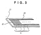
Figure 3 shows an example of the device in which N image sensors 1, of which one is illustrated in Figure 1, are provided in series on a ceramic substrate 21 carrying a heat generating cell array 20 for printing, and in which the drive output terminal 6₁, 6₂...6n of each image sensor 1 are connected to each heat generating cell of the heat generating array 20 by a group of wires 22 on a one to one basis.
-
In the case of this device, heat generated by the heat generating cell array 20 is transmitted to the image sensor 1, raising the temperature higher than the ambient temperature, but in the case where the image sensor does not supply only a binary output representing thick and thin as in an ordinary facsimile machine, problems do not occur even when photo-diodes which result in a heavy leak current under the high temperature condition are used in the image sensor. In the case where the thick and thin conditions of a document are read with output values of several levels to make a multi-level display, distinctive thick and thin images can be read with only an extremely small rise in dark output due to the temperature rise by employing floating base type photo-transistors. More over, a variety of elements may be used as the drive cell, an open drain type n-channel MOS transistor formed on a P type substrate being most suitable.
-
According to the present invention, circuit portions manufactured in the same semi-conductor integrated circuit process are formed on the same substrate as the image sensor. Thereby, not only can the size of the device be reduced, but also only a single manufacturing process is required. Accordingly, the manufacturing cost can be reduced remarkably in comparison with the known manufacturing process, in which the circuit components are produced separately.