EP0318395A2 - An apparatus for metal organic chemical vapor deposition and a method using the same - Google Patents
An apparatus for metal organic chemical vapor deposition and a method using the same Download PDFInfo
- Publication number
- EP0318395A2 EP0318395A2 EP88402977A EP88402977A EP0318395A2 EP 0318395 A2 EP0318395 A2 EP 0318395A2 EP 88402977 A EP88402977 A EP 88402977A EP 88402977 A EP88402977 A EP 88402977A EP 0318395 A2 EP0318395 A2 EP 0318395A2
- Authority
- EP
- European Patent Office
- Prior art keywords
- gas
- substrate
- metal organic
- reactor chamber
- pipes
- Prior art date
- Legal status (The legal status is an assumption and is not a legal conclusion. Google has not performed a legal analysis and makes no representation as to the accuracy of the status listed.)
- Granted
Links
Images


Classifications
-
- H—ELECTRICITY
- H01—ELECTRIC ELEMENTS
- H01L—SEMICONDUCTOR DEVICES NOT COVERED BY CLASS H10
- H01L21/00—Processes or apparatus adapted for the manufacture or treatment of semiconductor or solid state devices or of parts thereof
- H01L21/02—Manufacture or treatment of semiconductor devices or of parts thereof
- H01L21/04—Manufacture or treatment of semiconductor devices or of parts thereof the devices having at least one potential-jump barrier or surface barrier, e.g. PN junction, depletion layer or carrier concentration layer
- H01L21/18—Manufacture or treatment of semiconductor devices or of parts thereof the devices having at least one potential-jump barrier or surface barrier, e.g. PN junction, depletion layer or carrier concentration layer the devices having semiconductor bodies comprising elements of Group IV of the Periodic System or AIIIBV compounds with or without impurities, e.g. doping materials
- H01L21/20—Deposition of semiconductor materials on a substrate, e.g. epitaxial growth solid phase epitaxy
- H01L21/205—Deposition of semiconductor materials on a substrate, e.g. epitaxial growth solid phase epitaxy using reduction or decomposition of a gaseous compound yielding a solid condensate, i.e. chemical deposition
-
- C—CHEMISTRY; METALLURGY
- C23—COATING METALLIC MATERIAL; COATING MATERIAL WITH METALLIC MATERIAL; CHEMICAL SURFACE TREATMENT; DIFFUSION TREATMENT OF METALLIC MATERIAL; COATING BY VACUUM EVAPORATION, BY SPUTTERING, BY ION IMPLANTATION OR BY CHEMICAL VAPOUR DEPOSITION, IN GENERAL; INHIBITING CORROSION OF METALLIC MATERIAL OR INCRUSTATION IN GENERAL
- C23C—COATING METALLIC MATERIAL; COATING MATERIAL WITH METALLIC MATERIAL; SURFACE TREATMENT OF METALLIC MATERIAL BY DIFFUSION INTO THE SURFACE, BY CHEMICAL CONVERSION OR SUBSTITUTION; COATING BY VACUUM EVAPORATION, BY SPUTTERING, BY ION IMPLANTATION OR BY CHEMICAL VAPOUR DEPOSITION, IN GENERAL
- C23C16/00—Chemical coating by decomposition of gaseous compounds, without leaving reaction products of surface material in the coating, i.e. chemical vapour deposition [CVD] processes
- C23C16/44—Chemical coating by decomposition of gaseous compounds, without leaving reaction products of surface material in the coating, i.e. chemical vapour deposition [CVD] processes characterised by the method of coating
- C23C16/455—Chemical coating by decomposition of gaseous compounds, without leaving reaction products of surface material in the coating, i.e. chemical vapour deposition [CVD] processes characterised by the method of coating characterised by the method used for introducing gases into reaction chamber or for modifying gas flows in reaction chamber
-
- Y—GENERAL TAGGING OF NEW TECHNOLOGICAL DEVELOPMENTS; GENERAL TAGGING OF CROSS-SECTIONAL TECHNOLOGIES SPANNING OVER SEVERAL SECTIONS OF THE IPC; TECHNICAL SUBJECTS COVERED BY FORMER USPC CROSS-REFERENCE ART COLLECTIONS [XRACs] AND DIGESTS
- Y10—TECHNICAL SUBJECTS COVERED BY FORMER USPC
- Y10S—TECHNICAL SUBJECTS COVERED BY FORMER USPC CROSS-REFERENCE ART COLLECTIONS [XRACs] AND DIGESTS
- Y10S438/00—Semiconductor device manufacturing: process
- Y10S438/935—Gas flow control
Definitions
- This invention relates to an apparatus used for metal organic chemical vapor deposition (hereinafter, abbreviated as MOCVD) and a method using the same. Particularly, this invention concerns the apparatus and the method for growing a compound semiconductor layer on a substrate.
- This invention has a particular applicability in connection with an apparatus, in which a metal organic gas and a reactive gas therewith are comprised as source material gases and a hydrogen gas is used as a dilution gas.
- MOCVD metal organic vapor phase epitaxy
- a horizontal or vertical type reaction chamber is used in the MOCVD method.
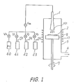
- FIG. 1 an MOCVD apparatus is schematically shown wherein a vertical type reactor chamber is used.
- a horizontal type reactor chamber is more suitable than the vertical type when plural wafers are processed at a time.
- the vertical type MOCVD apparatus has many advantages.
- a plurality of source material gases and a hydrogen dilution gas are mixed and fed into a reactor chamber 5 through a main valve V m and a vent pipe 1.
- Th vent pipe 1 is sealed to an upper wall portion of the reactor chamber 5 and broadens toward its opening 101.
- a wafer or a substrate 2 is loaded on a susceptor 8, facing the opening 101 and the susceptor is rotated about a support axis 7 during operation.
- the vent pipe 1 of a reversed funnel-like shape provides a uniform gas flow onto the surface of the substrate 2.
- the susceptor 8 is made of carbon material and is heated by a high frequency induction coil 17 in order to raise the substrate temperature to a specified value. Used gas is finally discharged through an opening 6.
- Source material gases are provided by a plurality of material gas sources 41 to 43 and mixed through valves V1, V2 and V3.
- three source material gas sources are representatively shown.
- a hydrogen dilution gas source 40 is provided and the hydrogen [H2] gas is supplied through a valve V0 and mixed with source material gases in order to control the gas flow rate and obtain a uniformly mixed gas.
- Each source material gas is provided in either a tank containing a source material gas or in a bubbler containing a metal organic compound source in a liquid or solid phase which is bubbled by a hydrogen gas.
- a ternary semiconductor GaAsP of InGaAs is grown on a binary semiconductor substrate of GaAs or InP respectively, three material gas sources are provided.
- indium gas source trimethylindium [In(CH3) 3] is provided in a bubbler
- gallium gas source trimethylgallium [Ga(CH3)3] is provided in a bubbler.
- arsenic or phosphorus gas source an arsine [ AsH3] or phosphine [ PH3] gas is provided in a tank.
- a bubbler containing the metal organic compound is bubbled with a hydrogen gas.
- the quantity of the metal organic compound output from the bubbler is controlled by the inside temperature of the bubbler and the flow rate of the bubbling hydrogen gas.
- the arsine or phosphine gas from the tank is also mixed with a hydrogen gas in order to increase a flow velocity in the pipe lines.
- the ratio of the V group source material to the III group source material in the mixed gas is maintained at a suitable value in order to obtain a proper growth rate and a proper mixing ratio of the grown mixed semiconductor. These factors change depending on the kinds of the semiconductor layer to be grown.
- the mixed gas of these source material gases is further diluted with a hydrogen gas from the dilution gas source 40 and thereafter fed to the reactor chamber 5.
- the most important objective in growing a compound semiconductor layer on a substrate is to obtain a uniform thickness of the grown layer over the entire surface of the substrate and further, when the grown semiconductor is a mixed compound semiconductor to ensure that the mixing ratio thereof is also as uniform as possible on the substrate surface.
- the latter condition can be expressed in other terms : that the grown semiconductor, for example, In 1-x Ga x As or In 1-x Ga x As y P 1-y has an almost constant x-value or (x, y)-value over the entire substrate surface.
- a vent pipe 1 shown in Fig. 2 has been proposed.
- the vent pipe 1 is provided with a plurality of branched pipes 3 at the spouting end thereof.
- the MOCVD apparatus utilizing the vent pipe such as shown in Fig. 2 is effective to some extent, however, it necessitates a vent pipe 1 having branched pipes 3 of varying diameter and shape.
- vent pipe when a gas flow rate, a growth temperature, etc. or the kinds of gases are changed, another type of the vent pipe must be provided, which has branched pipes of different diameter in order to obtain uniform growth on the substrate. It is difficult if not practically impossible to change the vent pipe during the growing process in order to obtain a different semiconductor layer.
- the above two disclosures relate to an MOCVD apparatus in which two gas sources are separately introduced into a reactor chamber and spouted from a plurality of distribution nozzles or branched vent pipes and mixed in the vicinity of the substrate. These disclosures have for main objective to avoid a mutual reaction between two source material gases before they are spouted into the reactor chamber. However, there still remain problems concerning the rendering of the gas flow rate, mixing ratio of gases, density of the mixed gas, etc. more uniform.
- an MOCVD apparatus in which a semiconductor substrate in a reactor chamber is rotated around its central axis and the substrate surface is arranged perpendicular to a plurality of vent pipes, thereby the diluted source material gas being spouted out in a direction substantially perpendicular to the substrate surface, with the gas flow rate through each vent pipe being adjustable or controllable. Further improvement of the apparatus can be achieved by adding a control mechanism for the dilution rate of the source material gas flowing through each vent pipe.
- Fig. 3 is a schematic gas flow diagram including a cross section of a reactor chamber of the first embodiment according to the present invention.
- a cylindrical body 11 of a reactor chamber 5 is made of quartz glass and has a diameter of, for example, about 100 mm.
- the reactor chamber 5 has a metal cover 10 of stainless steel at an upper end portion of the cylindrical body 11 and the cover 10 is sealed with the body.
- vent pipes are illustrated as if there were a considerable gap between the vent pipes. In an actual structure, however, there is almost no gap, the vent pipes having an inside diameter of 8 mm and being arranged with an axial distance of 10 mm.
- a perspective view of the vent pipes is shown in Fig. 7(a).
- Spouting ends 108 of the vent pipes face the substrate 2 at a distance of about 50 mm therefrom.
- the semiconductor substrate 2, on which a compound semiconductor layer is to be grown, is loaded onto a susceptor 8 of sintered carbon, having a diameter of about 70 mm.
- the lower end portion of the cylindrical body 11 is sealed to a base member 12 of stainless steel using an O -ring (not shown) and an exhaust outlet 6 is provided on a side wall of the base member 12.
- the outlet 6 is connected to an exhaust system 18 when a low pressure MOCVD method is utilized.
- the susceptor 8 is supported by a support rod 7, which penetrates through the bottom portion of the base member 12 and is rotatable airtightly about its axis utilizing an O -ring or a fluid magnetic seal (not shown).
- the support rod 7 is rotated by a driving mechanism 19 during the operation.
- the special feature of the present invention is characterized by the gas supply system for source material gases and a dilution gas to be introduced into the reactor chamber.
- a gas supply system for source material gases and a dilution gas to be introduced into the reactor chamber In Fig. 3, four vent pipes 111 to 114 of quartz glass are arranged colinearly and penetrate through the cover 10 and are sealed thereto.
- a gas flow control valve 13 to 16 is provided upstream, between a main pipe 20 and the inlet end 110 of each vent pipe.
- the main pipe feeds the diluted mixed source material gas, the flow thereof being closed or opened by a main valve V m .
- the main valve V m is connected to a dilution gas source 40 and source material gas sources 41, 42, and 43. In Fig. 3, these gas sources are schematically illustrated.
- a dilution gas source 40 is provided in a tank 50 containing hydrogen [ H2] gas and its flow rate is controlled by a mass flow controller MFC1 (mass flow controller is hereinafter abbreviated MFC).
- An indium gas source 41 is provided in a bubbler 51, containing trimethylindium [ In(CH3)3] , which is bubbled by hydrogen [ H2] gas introduced through a MFC2.
- the hydrogen [ H2] gas transports trimethylindium [ In(CH3)3] vapor and is further mixed with a hydrogen [ H2] gas supplied through a MFC3.
- a phosphorous gas source 42 is provided in a tank 52 containing a phosphine [PH3] gas, and is fed through a MFC4 and further mixed with a hydrogen gas supplied through MFC5.
- a metal organic gas containing vapor such as trimethylindium [In(CH3)3] reacts easily with a metal hydride gas such as phosphine [PH3] , or arsine [AsH3] in a heated atmosphere and deposits a compound on the substrate.
- a metal hydride gas such as phosphine [PH3]
- arsine [AsH3] in a heated atmosphere and deposits a compound on the substrate.
- a hydrogen dilution gas source such as denoted by 40 is provided separately in order to obtain uniformity of the mixed source material gas.
- the introduction of hydrogen gas into each material gas source 41 to 43 such as shown in Figs. 3 and 4 permits bubbling of a metal organic source or mixing of output from the tank in order to obtain a precise flow rate of the source material gas by increasing the gas flow velocity.
- a gallium gas source is prepared in a bubbler containing trimethylgallium [Ga(CH3)3] or triethylgallium [Ga(C2H5)3] bubbled with a hydrogen gas
- an arsenic gas source is prepared in a tank containing an arsine [AsH3] gas.
- the gas source system comprising three material gas sources and the dilution gas source is provided, three material gas sources being selected among the gallium, indium, arsenic and phosphorous gas sources. These source material gases are mixed and diluted with the hydrogen dilution gas before use. While feeding the above diluted mixed source material gas into the reactor chamber, the GaAs of InP substrate loaded onto the susceptor 8 is rotated at a speed of about 60 rpm, and is heated by a high frequency induction coil 17 disposed outside the reactor chamber 5. The substrate temperature is raised to about 650°C.
- the main pipe 20 is branched into four branch pipes 21 to 24, where the diluted and mixed source material gas is divided.
- the gas flow rate through each branch pipe is controlled by a gas flow control valve 13 to 16.
- the gas flow control valve in Fig. 3 is shown by a simplified symbol, however, in an actual application, a combination of a needle valve and a mass flow meter, or a mass flow controller (MFC) is utilized.
- the gas flow rate in each branch pipe is determined such that the grown semiconductor GaAsP or InGaAs layer has as uniform a thickness and alignment composition as possible. Therefore, the gas flow rate changes depending upon the kinds of gases, the temperature of the substrate, the pressure in the reactor chamber, etc.
- the gas flow rate through branch pipes 21 and 24 is maintained at 1500 SCCM (standard cubic centimetres per minute) and the gas flow rate through branch pipes 22 and 23 is maintained at 1000 SCCM. This is because the gas flow rate directed toward the peripheral portion of the circular substrate surface should be larger than that directed toward the central portion thereof for obtaining the uniform thickness.
- FIGs. 5(a) and 5(b) An InGaAs layer having 1 ⁇ m thickness is grown on an InP substrate of 50 mm in diameter.
- Fig. 5(a) shows a thickness fluctuation along the diameter of the substrate and
- Fig. 5(b) shows a fluctuation of composition along the diameter, in which x denotes a mixing ratio of the mixed compound semiconductor InGaAs when it is represented by a formula In 1-x Ga x As.
- the dashed curve shows a test result of the grown InGaAs layer obtained by the prior art method
- the solid curve shows a test result according to the above embodiment.
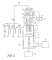
- Fig. 6 is a schematic gas flow diagram including a schematic cross section of a reactor chamber in accordance with the second embodiment of the present invention. Most of the structure is similar to that shown in Fig. 3 except that an automatic gas flow control system is added to the gas flow passages of branch pipes 21 to 24.
- a mass flow meter 25 to 28 and a flow adjustment valve 29 to 32 such as a needle valve, which responds to an electric signal, are inserted into each branch pipe 21 to 24.
- a controller 33 comprising a microprocessor 34 and a memory unit 35, is operatively connected to each of the above mass flow meters and flow adjustment valves.
- the combination of a mass flow meter and a flow adjustment valve can be replaced by an MFC, which serves to control and maintain the gas flow rate at a predetermined value.
- the memory unit 35 stores the necessary data relative to the gas flow rate in each branch pipe, the required growth time in each step, etc. With a start command to the controller 33, the microprocessor 34 begins to read the data stored in the memory unit 35, compares these data with the measured flow rate in each branch pipe and controls the gas flow rate according to the predetermined data.
- all source material gases and the hydrogen dilution gas are mixed and diluted in the gas source system and thereafter divided and fed to each branch pipe.
- the mixed gas is flowing through the main pipe 20 or branch pipes at a very low velocity, which is often the case in a normal pressure MOCVD method, the mixed gases are liable to react mutually even when flowing through the pipe, resulting in the depositing of formed material onto the inside wall of the pipes.
- Fig. 7(a) shows a schematic perspective view of the vent pipes 111 to 114 fixed to the cover 10, which appears in Fig. 3, in a manner which has already been described
- Fig. 7(b) shows a similar view of the third embodiment with an additional set of vent pipes 111a and 114a provided.
- FIG. 8 shows a schematic gas flow diagram of the fourth embodiment of the present invention.
- a gas source system 36 comprises a dilution gas source 40 and a plurality of source material gas sources, which are illustrated simply by a mixed material gas source 37 in Fig. 8.
- an outlet of the dilution gas source 40 is not connected directly to the main pipe as shown in Fig. 3, but connected separately to a dilution gas supply pipe 38.
- the outlet of the mixed material gas source 37 is connected to a material gas supply pipe 39.
- the dilution gas supply pipe 38 is branched into four dilution gas branch pipes 71 to 74.
- the material gas supply pipe 39 is also branched into four material branch pipes 61 to 64.
- a mass flow controller denoted as MFC61 to MFC64 and MFC71 to MFC74 is inserted.
- each end of the dilution gas branch pipes 71 to 74 is connected with each respective outlet side of MFC61 to MFC64 of the material gas branch pipes 61 to 64.
- the material gas branch pipes 61 to 64 are finally connected to respective vent pipes 111 to 114.
- the mixed material gas source 37 supplies a mixed gas of trimethylindium [In(CH3)3] and phosphine [PH3], having a mixing ratio of 1:100.
- the dilution gas source 40 supplies a hydrogen [H2] dilution gas.
- the growth rate of InP layer on the substrate is proportional to a concentration of the source material gas, in this case, trimethylindium [In(CH3)3] and a square root of the velocity of gas flow on the substrate surface.
- the source material gas in this case, trimethylindium [In(CH3)3] and a square root of the velocity of gas flow on the substrate surface.
- Fig. 9 illustrates the path of the gas flow schematically in the region from the spouting ends of the vent pipes 111 to 114 onto the substrate 2.
- the concentration of trimethylindium [In(CH3)3] in the diluted mixed gas through two vent pipes 111 and 114 disposed on either side is chosen to be higher than the concentration through vent pipes 112 and 113 disposed in the center.
- the growth rate of the semiconductor InP on the substrate is schematically shown by the curves 81 and 82 in Fig. 10.
- the direction A-A in Fig. 10 corresponds to the direction A-A in Fig. 9.
- the growth rate on the peripheral portion of the substrate is higher than that on the central portion thereof.
- the growth rate on the peripheral portion is lower than that on the central portion.
- Test results for growing the InP layer having a thickness of 2 ⁇ m show that a thickness fluctuation within a 2 ⁇ m ⁇ 0.02 ⁇ m range can be obtained, a remarkable improvement compared with the results of the order of 2 ⁇ m ⁇ 0.06 ⁇ m of the prior art.
- vent pipes are aligned perpendicular to the substrate, spouting ends thereof facing toward the substrate and disposed symmetrically with regard to the center of the substrate.
- vent pipes and branch pipes are not limited to any specific number, such as four ; and, moreover, vent pipes are not limited to colinear arrangement. Spouting ends of vent pipes may be arranged two-dimensionally, or asymmetrically with regard to the center of the substrate surface.
Abstract
Description
- This invention relates to an apparatus used for metal organic chemical vapor deposition (hereinafter, abbreviated as MOCVD) and a method using the same. Particularly, this invention concerns the apparatus and the method for growing a compound semiconductor layer on a substrate. This invention has a particular applicability in connection with an apparatus, in which a metal organic gas and a reactive gas therewith are comprised as source material gases and a hydrogen gas is used as a dilution gas.
- An MOCVD method is widely used when a compound semiconductor such as a group III-V or II-VI binary, ternary, or quaternary semiconductor is grown on a semiconductor substrate. In the MOCVD method, a compound gas composed of metal and methyl (or ethyl) group is used as one of source material gases, and is fed to a reactor chamber bubbled with a hydrogen gas. Although the process is sometimes called MOVPE (metal organic vapor phase epitaxy), the word "MOCVD" is used hereinafter in relation to the present invention.
- A horizontal or vertical type reaction chamber is used in the MOCVD method. In Fig. 1, an MOCVD apparatus is schematically shown wherein a vertical type reactor chamber is used. A horizontal type reactor chamber is more suitable than the vertical type when plural wafers are processed at a time. However, when uniformity in the thickness or composition of a grown compound semiconductor layer is important, the vertical type MOCVD apparatus has many advantages.
- In Fig. 1, a plurality of source material gases and a hydrogen dilution gas are mixed and fed into a
reactor chamber 5 through a main valve Vm and avent pipe 1.Th vent pipe 1 is sealed to an upper wall portion of thereactor chamber 5 and broadens toward itsopening 101. A wafer or asubstrate 2 is loaded on asusceptor 8, facing theopening 101 and the susceptor is rotated about asupport axis 7 during operation. Thevent pipe 1 of a reversed funnel-like shape provides a uniform gas flow onto the surface of thesubstrate 2. Thesusceptor 8 is made of carbon material and is heated by a highfrequency induction coil 17 in order to raise the substrate temperature to a specified value. Used gas is finally discharged through anopening 6. - Source material gases are provided by a plurality of
material gas sources 41 to 43 and mixed through valves V₁, V₂ and V₃. In Fig. 1, three source material gas sources are representatively shown. Generally, a hydrogendilution gas source 40 is provided and the hydrogen [H₂] gas is supplied through a valve V₀ and mixed with source material gases in order to control the gas flow rate and obtain a uniformly mixed gas. Each source material gas is provided in either a tank containing a source material gas or in a bubbler containing a metal organic compound source in a liquid or solid phase which is bubbled by a hydrogen gas. For example, when a ternary semiconductor GaAsP of InGaAs is grown on a binary semiconductor substrate of GaAs or InP respectively, three material gas sources are provided. As an indium gas source, trimethylindium [In(CH₃) ₃] is provided in a bubbler, and as a gallium gas source, trimethylgallium [Ga(CH₃)₃] is provided in a bubbler. As an arsenic or phosphorus gas source, an arsine [ AsH₃] or phosphine [ PH₃] gas is provided in a tank. - In order to use these metal organic gas sources, a bubbler containing the metal organic compound is bubbled with a hydrogen gas. The quantity of the metal organic compound output from the bubbler is controlled by the inside temperature of the bubbler and the flow rate of the bubbling hydrogen gas. On the other hand, the arsine or phosphine gas from the tank is also mixed with a hydrogen gas in order to increase a flow velocity in the pipe lines. In growing a III-V group semiconductor layer, the ratio of the V group source material to the III group source material in the mixed gas is maintained at a suitable value in order to obtain a proper growth rate and a proper mixing ratio of the grown mixed semiconductor. These factors change depending on the kinds of the semiconductor layer to be grown. In order to control the growth process easily and obtain a uniform mixture of source material gases, the mixed gas of these source material gases is further diluted with a hydrogen gas from the
dilution gas source 40 and thereafter fed to thereactor chamber 5. - The most important objective in growing a compound semiconductor layer on a substrate is to obtain a uniform thickness of the grown layer over the entire surface of the substrate and further, when the grown semiconductor is a mixed compound semiconductor to ensure that the mixing ratio thereof is also as uniform as possible on the substrate surface. The latter condition can be expressed in other terms : that the grown semiconductor, for example, In1-xGaxAs or In1-xGaxAsyP1-y has an almost constant x-value or (x, y)-value over the entire substrate surface.
- However in an application of the MOCVD apparatus shown in Fig. 1, though it has the vent pipe1 which has the enlarged
end opening 101 from which gas is spouted into the reactor chamber in order to provide a more uniform gas flow onto the substrate surface, it is a difficult matter to obtain a uniform thickness of the grown layer over the entire substrate surface as well as a uniform composition thereof. To improve the uniformity of the gas flow, avent pipe 1 shown in Fig. 2 has been proposed. Thevent pipe 1 is provided with a plurality ofbranched pipes 3 at the spouting end thereof. The MOCVD apparatus utilizing the vent pipe such as shown in Fig. 2 is effective to some extent, however, it necessitates avent pipe 1 having branchedpipes 3 of varying diameter and shape. And moreover, when a gas flow rate, a growth temperature, etc. or the kinds of gases are changed, another type of the vent pipe must be provided, which has branched pipes of different diameter in order to obtain uniform growth on the substrate. It is difficult if not practically impossible to change the vent pipe during the growing process in order to obtain a different semiconductor layer. - Other improvements for obtaining uniformity of the grown semiconductor layer, especially, with regard to the vertical type MOCVD apparatus are disclosed in the following Japnese Unexamined Patent Publications :
- SHO-58-176196 dated October 15, 1983, by A. Takamori etal.
- SHO-60-189928 dated September 27, 1985, by Y. Shiotani.
- The above two disclosures relate to an MOCVD apparatus in which two gas sources are separately introduced into a reactor chamber and spouted from a plurality of distribution nozzles or branched vent pipes and mixed in the vicinity of the substrate. These disclosures have for main objective to avoid a mutual reaction between two source material gases before they are spouted into the reactor chamber. However, there still remain problems concerning the rendering of the gas flow rate, mixing ratio of gases, density of the mixed gas, etc. more uniform.
- It is a general object of the invention to provide an MOCVD apparatus for growing a compound semiconductor layer on a substrate with a hitherto unobtainable degree of uniformity.
- It is a more specific object of the invention to provide an MOCVD apparatus for growing a compound semiconductor layer with a superior degree of uniformity in thickness of the grown compound semiconductor layer over an entire surface of the substrate.
- It is another object of the invention to provide an MOCVD apparatus for growing a compound semiconductor layer with a superior degree of uniformity in composition of the grown compound semiconductor layer over an entire surface of the substrate.
- It is still another object of the invention to provide a method of growing a semiconductor layer utilizing the above-described MOCVD apparatus for obtaining a superior uniformity in thickness and composition of the grown semiconductor layer.
- It is further object of the invention to provide the above method of growing a compound semiconductor layer, in which the growing process is automatically controlled.
- According to the present invention, these and other objects and advantages are achieved by an MOCVD apparatus, in which a semiconductor substrate in a reactor chamber is rotated around its central axis and the substrate surface is arranged perpendicular to a plurality of vent pipes, thereby the diluted source material gas being spouted out in a direction substantially perpendicular to the substrate surface, with the gas flow rate through each vent pipe being adjustable or controllable. Further improvement of the apparatus can be achieved by adding a control mechanism for the dilution rate of the source material gas flowing through each vent pipe.
- Further objects and advantages of the present invention will be apparent from the following description, reference being made to the accompanying drawing wherein preferred embodiments of the present invention are clearly shown.
-
- Figs. 1 and 2 show schematically a cross section of a reactor chamber and a gas flow diagram of an MOCVD apparatus of the prior art, wherein two different vent pipe structures are shown respectively,
- Fig. 3 shows schematically a cross section of a reactor chamber and a gas flow diagram of an MOCVD apparatus in accordance with the first embodiment of the present invention,
- Fig. 4 shows a schematic diagram of a gas source system used in the present invention,
- Figs. 5(a) and 5(b) show a comparison test result on a thickness and an x-value respectively in growing a GaAsP layer on a substrate, wherein a solid curve shows the data obtained by the present invention and a dashed curve, by the prior art technology,
- Fig. 6 shows the second embodiment of the present invention, in which each gas flow through the vent pipes is automatically controlled by a controller,
- Figs. 7(a) and 7(b) show a perspective view of the vent pipes of the first and second embodiments respectively,
- Fig. 8 shows a gas flow diagram of the fourth embodiment of the present invention,
- Fig. 9 illustrates gas flow paths from the vent pipes onto the substrate, and
- Fig. 10 illustrates schematically a thickness distribution of the grown semiconductor on the substrate according to the present invention assuming that the substrate is stationary with regard to the reactor chamber.
- In the following explanation of the embodiments, same or like reference numerals designate same or corresponding parts previously referenced in Figs. 1 and 2.
- Fig. 3 is a schematic gas flow diagram including a cross section of a reactor chamber of the first embodiment according to the present invention. A
cylindrical body 11 of areactor chamber 5 is made of quartz glass and has a diameter of, for example, about 100 mm. Thereactor chamber 5 has ametal cover 10 of stainless steel at an upper end portion of thecylindrical body 11 and thecover 10 is sealed with the body. A plurality ofvent pipes 111 to 114 sealed with thecover 10 using O-rings (not shown), penetrate vertically therethrough, the seal position being aligned in the diametrical direction of thecover 10. In Fig. 3, vent pipes are illustrated as if there were a considerable gap between the vent pipes. In an actual structure, however, there is almost no gap, the vent pipes having an inside diameter of 8 mm and being arranged with an axial distance of 10 mm. A perspective view of the vent pipes is shown in Fig. 7(a). - Spouting ends 108 of the vent pipes face the
substrate 2 at a distance of about 50 mm therefrom. Thesemiconductor substrate 2, on which a compound semiconductor layer is to be grown, is loaded onto asusceptor 8 of sintered carbon, having a diameter of about 70 mm. - The lower end portion of the
cylindrical body 11 is sealed to abase member 12 of stainless steel using an O-ring (not shown) and anexhaust outlet 6 is provided on a side wall of thebase member 12. Theoutlet 6 is connected to anexhaust system 18 when a low pressure MOCVD method is utilized. Thesusceptor 8 is supported by asupport rod 7, which penetrates through the bottom portion of thebase member 12 and is rotatable airtightly about its axis utilizing an O-ring or a fluid magnetic seal (not shown). Thesupport rod 7 is rotated by adriving mechanism 19 during the operation. - The special feature of the present invention is characterized by the gas supply system for source material gases and a dilution gas to be introduced into the reactor chamber. In Fig. 3, four
vent pipes 111 to 114 of quartz glass are arranged colinearly and penetrate through thecover 10 and are sealed thereto. A gasflow control valve 13 to 16 is provided upstream, between amain pipe 20 and the inlet end 110 of each vent pipe. The main pipe feeds the diluted mixed source material gas, the flow thereof being closed or opened by a main valve Vm. The main valve Vm is connected to adilution gas source 40 and sourcematerial gas sources - An actual gas source system is shown in Fig. 4. for the simple case of InP grown on a binary substrate InP. A
dilution gas source 40 is provided in atank 50 containing hydrogen [ H₂] gas and its flow rate is controlled by a mass flow controller MFC₁ (mass flow controller is hereinafter abbreviated MFC). Anindium gas source 41 is provided in a bubbler 51, containing trimethylindium [ In(CH₃)₃] , which is bubbled by hydrogen [ H₂] gas introduced through a MFC₂. The hydrogen [ H₂] gas transports trimethylindium [ In(CH₃)₃] vapor and is further mixed with a hydrogen [ H₂] gas supplied through a MFC₃. Aphosphorous gas source 42 is provided in atank 52 containing a phosphine [PH₃] gas, and is fed through a MFC₄ and further mixed with a hydrogen gas supplied through MFC₅. - A metal organic gas containing vapor such as trimethylindium [In(CH₃)₃] reacts easily with a metal hydride gas such as phosphine [PH₃] , or arsine [AsH₃] in a heated atmosphere and deposits a compound on the substrate. However, in order to deposit a compound semiconductor layer having a uniform thickness and composition, the method of introducing these gases into a reactor chamber is an important problem. Generally, a hydrogen dilution gas source such as denoted by 40 is provided separately in order to obtain uniformity of the mixed source material gas. On the other hand, the introduction of hydrogen gas into each
material gas source 41 to 43 such as shown in Figs. 3 and 4 permits bubbling of a metal organic source or mixing of output from the tank in order to obtain a precise flow rate of the source material gas by increasing the gas flow velocity. - Though only three gas sources are illustrated in Fig. 4, other source material gases are added into the gas source system when necessary. For example, a gallium gas source is prepared in a bubbler containing trimethylgallium [Ga(CH₃)₃] or triethylgallium [Ga(C₂H₅)₃] bubbled with a hydrogen gas, and an arsenic gas source is prepared in a tank containing an arsine [AsH₃] gas.
- When a InGaP or InGaAs layer is grown on a GaAs or InP substrate respectively, the gas source system comprising three material gas sources and the dilution gas source is provided, three material gas sources being selected among the gallium, indium, arsenic and phosphorous gas sources. These source material gases are mixed and diluted with the hydrogen dilution gas before use. While feeding the above diluted mixed source material gas into the reactor chamber, the GaAs of InP substrate loaded onto the
susceptor 8 is rotated at a speed of about 60 rpm, and is heated by a highfrequency induction coil 17 disposed outside thereactor chamber 5. The substrate temperature is raised to about 650°C. - In the first embodiment, the
main pipe 20 is branched into fourbranch pipes 21 to 24, where the diluted and mixed source material gas is divided. The gas flow rate through each branch pipe is controlled by a gasflow control valve 13 to 16. The gas flow control valve in Fig. 3 is shown by a simplified symbol, however, in an actual application, a combination of a needle valve and a mass flow meter, or a mass flow controller (MFC) is utilized. The gas flow rate in each branch pipe is determined such that the grown semiconductor GaAsP or InGaAs layer has as uniform a thickness and alignment composition as possible. Therefore, the gas flow rate changes depending upon the kinds of gases, the temperature of the substrate, the pressure in the reactor chamber, etc. For example, the gas flow rate throughbranch pipes branch pipes - One test result is shown in Figs. 5(a) and 5(b). An InGaAs layer having 1 µm thickness is grown on an InP substrate of 50 mm in diameter. Fig. 5(a) shows a thickness fluctuation along the diameter of the substrate and Fig. 5(b) shows a fluctuation of composition along the diameter, in which x denotes a mixing ratio of the mixed compound semiconductor InGaAs when it is represented by a formula In1-xGaxAs. In the two figures, the dashed curve shows a test result of the grown InGaAs layer obtained by the prior art method, and the solid curve shows a test result according to the above embodiment.
- As shown in Fig. 5(a), the fluctuation in thickness, ranging from +10 % to -10 % in the prior art is reduced to within a ±
range 3% range by utilizing the MOCVD apparatus of the first embodiment. Furthermore, as shown in Fig. 5(b), when the In1-xGaxAs layer is grown with the aim of obtaining x = 0.53, the fluctuation of x-valve is improved from about a ± 10 % range to a ± 3 % range. Thus figure 5(b) shows that a remarkable improvement is achieved in uniformity of the composition. - Fig. 6 is a schematic gas flow diagram including a schematic cross section of a reactor chamber in accordance with the second embodiment of the present invention. Most of the structure is similar to that shown in Fig. 3 except that an automatic gas flow control system is added to the gas flow passages of
branch pipes 21 to 24. In Fig. 6, amass flow meter 25 to 28 and a flow adjustment valve 29 to 32 such as a needle valve, which responds to an electric signal, are inserted into eachbranch pipe 21 to 24. Moreover, acontroller 33 comprising amicroprocessor 34 and amemory unit 35, is operatively connected to each of the above mass flow meters and flow adjustment valves. The combination of a mass flow meter and a flow adjustment valve can be replaced by an MFC, which serves to control and maintain the gas flow rate at a predetermined value. Thememory unit 35 stores the necessary data relative to the gas flow rate in each branch pipe, the required growth time in each step, etc. With a start command to thecontroller 33, themicroprocessor 34 begins to read the data stored in thememory unit 35, compares these data with the measured flow rate in each branch pipe and controls the gas flow rate according to the predetermined data. - In the above first and second embodiment, all source material gases and the hydrogen dilution gas are mixed and diluted in the gas source system and thereafter divided and fed to each branch pipe. However, when the mixed gas is flowing through the
main pipe 20 or branch pipes at a very low velocity, which is often the case in a normal pressure MOCVD method, the mixed gases are liable to react mutually even when flowing through the pipe, resulting in the depositing of formed material onto the inside wall of the pipes. - In the third embodiment which prevents the above reaction of the mixed gases within the gas supply system, one source material gas, which reacts readily with other source material gases, is supplied separately in another gas supply system. In this case, the above reactive source material gas is spouted out separately from another set of vent pipes into the reactor chamber. Fig. 7(a) shows a schematic perspective view of the
vent pipes 111 to 114 fixed to thecover 10, which appears in Fig. 3, in a manner which has already been described, and Fig. 7(b) shows a similar view of the third embodiment with an additional set of vent pipes 111a and 114a provided. - Fig. 8 shows a schematic gas flow diagram of the fourth embodiment of the present invention. There is no change in the other parts of the MOCVD apparatus with the exception of the gas supply system, hence only the gas flow diagram is shown in the figure. A
gas source system 36 comprises adilution gas source 40 and a plurality of source material gas sources, which are illustrated simply by a mixedmaterial gas source 37 in Fig. 8. However, an outlet of thedilution gas source 40 is not connected directly to the main pipe as shown in Fig. 3, but connected separately to a dilutiongas supply pipe 38. The outlet of the mixedmaterial gas source 37 is connected to a materialgas supply pipe 39. The dilutiongas supply pipe 38 is branched into four dilutiongas branch pipes 71 to 74. The materialgas supply pipe 39 is also branched into fourmaterial branch pipes 61 to 64. In eachbranch pipe line 61 to 64 and 71 to 74, a mass flow controller denoted as MFC₆₁ to MFC₆₄ and MFC₇₁ to MFC₇₄ is inserted. Furthermore, each end of the dilutiongas branch pipes 71 to 74 is connected with each respective outlet side of MFC₆₁ to MFC₆₄ of the materialgas branch pipes 61 to 64. The materialgas branch pipes 61 to 64 are finally connected torespective vent pipes 111 to 114. - When an InP layer, for example, is grown on a substrate, the mixed
material gas source 37 supplies a mixed gas of trimethylindium [In(CH₃)₃] and phosphine [PH₃], having a mixing ratio of 1:100. Thedilution gas source 40 supplies a hydrogen [H₂] dilution gas. These two gases flow separately through the dilutiongas supply pipe 38 and materialgas supply pipe 39, and each gas flow is branched into four branch pipes. The flow rate in each branch pipe is precisely controlled by the MFC inserted in the branch pipe. It is known that the growth rate of InP layer on the substrate is proportional to a concentration of the source material gas, in this case, trimethylindium [In(CH₃)₃] and a square root of the velocity of gas flow on the substrate surface. In this embodiment, it becomes possible to control these two factors individually and more precisely. - Fig. 9 illustrates the path of the gas flow schematically in the region from the spouting ends of the
vent pipes 111 to 114 onto thesubstrate 2. The concentration of trimethylindium [In(CH₃)₃] in the diluted mixed gas through twovent pipes vent pipes substrate 2 is made stationary with regard to thevent pipes 111 to 114, the growth rate of the semiconductor InP on the substrate is schematically shown by thecurves substrate 2 is rotated about its central axis, while the gas flow rates through the twovent pipes vent pipes - Throughout the explanation of the preferred embodiments, four branch pipes and four vent pipes are used and illustrated, and vent pipes are aligned perpendicular to the substrate, spouting ends thereof facing toward the substrate and disposed symmetrically with regard to the center of the substrate.
- However, the present invention may be embodied in other specific forms of the gas supply system without departing from the spirit or essential characteristics thereof. The number of branch pipes and vent pipes is not limited to any specific number, such as four ; and, moreover, vent pipes are not limited to colinear arrangement. Spouting ends of vent pipes may be arranged two-dimensionally, or asymmetrically with regard to the center of the substrate surface.
Claims (18)
a reactor chamber (5) having an exhaust outlet (6) and a plurality of vent pipes (111, 112, 113, 114) of which one end protrudes into the reactor chamber (5) for spouting a mixed gas onto said substrate (2), and the direction of the gas spouting being arranged perpendicular to a surface of said substrate (2),
means (7, 8) for supporting and rotating said substrate (2) enclosed in said reactor chamber (5),
means (17) for heating said substrate disposed outside the reactor chamber (5),
a gas source means (40, 41, 42, 43) for supplying said mixed gas to a main pipe (20), said mixed gas comprising at least a metal organic gas and a reactive gas with said metal organic gas,
a plurality of branch pipes (21, 22, 23, 24) for feeding said mixed gas from said main pipe (20) to each of said vent pipes (111, 112, 113, 114), and
means (13, 14, 15, 16) for controlling a gas flow through said branch pipes.
a reactor chamber (5) having an exhaust outlet (6) and a first and a second group of vent pipes (111, 112, 113, 114) of which one end protrudes into the reactor chamber (5), the first group of said vent pipes being provided for spouting a first kind of gas comprising a metal organic gas onto said substrate (2) and the second group of said vent pipes for spouting a second kind of gas comprising a reactive gas with the said metal organic gas onto said substrate (2), both directions of the gas spouting being arranged perpendicular to a surface of said substrate (2), each of said first and second groups having substantially the same number of vent pipes, said number of vent pipes in each of said groups being at least two, and each vent pipe of the first group being arranged adjacent to respective vent pipe of the second group,
means (7, 8) for supporting and rotating said substrate (2) enclosed in said reactor chamber (5),
means (17) for heating said substrate disposed outside the reactor chamber (5),
a gas source means (40, 41, 42, 43) for supplying said first and second kinds of gas to a first and a second main pipe respectively,
two sets of branch pipes (21, 22, 23, 24) for feeding said first and second kinds of gas from said first and second main pipes to said first and second groups of vent pipes respectively, and
means (13, 14, 15, 16) for controlling a gas flow through said branch pipes.
a reactor chamber (5) having an exhaust outlet (6) and a plurality of vent pipes (111, 112, 113, 114) of which one end protrudes into the reactor (5) for spouting a diluted mixed gas onto said substrate (2), and the direction of the gas spouting being arranged perpendicular to a surface of said substrate (2),
means (7, 8) for supporting and rotating said substrate enclosed in said reactor chamber (5),
means (17) for heating said substrate disposed outside the reactor chamber (5),
a gas source means (37, 49) for supplying a mixed gas to a first main pipe (39) and a dilution gas to a second main pipe 38, said mixed gas comprising a metal organic gas and a reactive gas with said metal organic gas,
a first and a second set of branch pipes (61 to 64, 71 to 74), each set of the branch pipes having the same number of branch pipes as the said plurality of said vent pipes, one end of each of said first set of branch pipes (61 to 64) being connected to said first main pipe (39), and one end of each of said second set of branch pipes (71 to 74) being connected to said second main pipe (38), and the opposite end of each of said first set of branch pipes (61 to 64) being connected to a respective opposite end of each of said second set of branch pipes (71 to 74) and further connected to a respective inlet of said vent pipes (11 to 14), whereby said diluted mixed gas is supplied to each of said vent pipes, and
means (MFC 61 to 64, MFC 71 to 74) for controlling a gas flow through said branch pipes.
disposing said substrate (2) in a reactor chamber (5), said substrate being loaded on a support (8) and rotated about the center of said substrate,
heating said substrate by a heating means (17) disposed outside the reactor chamber (5),
flowing a mixed gas into the reactor chamber (5) through a plurality of vent pipes (111 to 114) and releasing the used mixed gas through an exhaust outlet (6) to the outside of the reactor chamber (5), and said mixed gas being spouted out onto the substrate surface substantially perpendicular thereto, wherein said mixed gas comprises at least a metal organic gas, and
controlling each gas flow rate through said vent pipes (111 to 114).
disposing said substrate (2) in a reactor chamber (5), said substrate being loaded on a support (8) and rotated about the center of said substrate,
heating said substrate by a heating means (17) disposed outside the reactor chamber (5),
flowing a first and a second kind of gas into the reactor chamber through a first and a second group of vent pipes (111 to 114, 111a to 114a) respectively and releasing the used gases through an exhaust outlet (6) to the outside of the reactor chamber (5), both said first and second kinds of gas being spouted out onto the substrate (2) substantially perpendicular thereto, wherein the first kind of gas comprises a metal organic gas and the second kind of gas comprises a reactive gas with said metal organic gas, and both said first and second groups of vent pipes having substantially the same number of vent pipes, said number of vent pipes in each of said groups being at least two, each vent pipe (111 to 114) of the first group being arranged adjacent to a respective vent pipe (111a to 114a) of the second group, and
controlling each gas flow rate through said vent pipes and thereby a mixing ratio of the first kind of gas to the second kind of gas spouted onto the substrate (2).
disposing said substrate in a reactor chamber (5), said substrate being loaded on a support (8) and rotated about the center of said substrate,
heating said substrate by a heating means (17) disposed outside the reactor chamber (5),
flowing a diluted mixed gas into the reactor chamber (5) through a plurality of vent pipes (111 to 114) and releasing the used gases through an exhaust outlet (6) to the outside of the reactor chamber (5), said diluted mixed gas being spouted out from the vent pipes substantially perpendicular to the substrate surface, wherein said diluted mixed gas is formed by mixing a mixed gas (27) and a dilution gas (40) supplied through a first and a second set of branch pipes (61 to 64, 71 to 74) respectively, both sets having the same number of branch pipes as that of said vent pipes (111 to 114), and said mixed gas comprises a metal organic gas and a reactive gas with said metal organic gas, and
controlling each gas flow rate through said branch pipes and thereby the concentration of the mixed gas in the diluted mixed gas.
Applications Claiming Priority (4)
| Application Number | Priority Date | Filing Date | Title |
|---|---|---|---|
| JP299158/87 | 1987-11-27 | ||
| JP62299158A JP2668687B2 (en) | 1987-11-27 | 1987-11-27 | CVD device |
| JP63248311A JPH0296324A (en) | 1988-09-30 | 1988-09-30 | Manufacture of semiconductor device and vapor growth device used for it |
| JP248311/88 | 1988-09-30 |
Publications (3)
| Publication Number | Publication Date |
|---|---|
| EP0318395A2 true EP0318395A2 (en) | 1989-05-31 |
| EP0318395A3 EP0318395A3 (en) | 1990-05-02 |
| EP0318395B1 EP0318395B1 (en) | 1993-10-06 |
Family
ID=26538710
Family Applications (1)
| Application Number | Title | Priority Date | Filing Date |
|---|---|---|---|
| EP88402977A Expired - Lifetime EP0318395B1 (en) | 1987-11-27 | 1988-11-25 | An apparatus for metal organic chemical vapor deposition and a method using the same |
Country Status (4)
| Country | Link |
|---|---|
| US (1) | US4980204A (en) |
| EP (1) | EP0318395B1 (en) |
| KR (1) | KR920010690B1 (en) |
| DE (1) | DE3884763T2 (en) |
Cited By (9)
| Publication number | Priority date | Publication date | Assignee | Title |
|---|---|---|---|---|
| EP0418554A2 (en) * | 1989-08-18 | 1991-03-27 | Fujitsu Limited | Chemical vapor deposition apparatus |
| EP0502209A1 (en) * | 1990-09-21 | 1992-09-09 | Fujitsu Limited | Method and apparatus for growing compound semiconductor crystals |
| EP0505251A2 (en) * | 1991-03-19 | 1992-09-23 | Fujitsu Limited | A method of growing group II-VI mixed compound semiconductor and an apparatus used therefor |
| EP0510791A2 (en) * | 1991-04-22 | 1992-10-28 | Applied Materials, Inc. | Flow verification for process gas in a wafer processing system, apparatus and method |
| EP0550058A2 (en) * | 1991-12-30 | 1993-07-07 | Texas Instruments Incorporated | A programmable multizone gas injector for single-wafer semiconductor processing equipment |
| EP0606737A1 (en) * | 1992-12-11 | 1994-07-20 | Shin-Etsu Handotai Company Limited | Process and apparatus for growing a silicon epitaxial layer, with a control of the mass flows of the reactive gases |
| US5453124A (en) * | 1992-12-30 | 1995-09-26 | Texas Instruments Incorporated | Programmable multizone gas injector for single-wafer semiconductor processing equipment |
| CN103966573A (en) * | 2013-01-29 | 2014-08-06 | 无锡华润上华科技有限公司 | Gas reaction device and method for PECVD thin film deposition |
| WO2023191939A1 (en) * | 2022-03-30 | 2023-10-05 | Applied Materials, Inc. | Packaging for a sensor and methods of manufacturing thereof |
Families Citing this family (88)
| Publication number | Priority date | Publication date | Assignee | Title |
|---|---|---|---|---|
| CA2008946C (en) * | 1989-01-30 | 1999-02-23 | Takayoshi Maeda | Vapor-phase epitaxial growth method |
| US5070813A (en) * | 1989-02-10 | 1991-12-10 | Tokyo Electron Limited | Coating apparatus |
| KR940011005B1 (en) * | 1989-09-09 | 1994-11-22 | 캐논 가부시끼가이샤 | Process for forming deposited film by use of alkyl aluminum hydride |
| CA2016970A1 (en) * | 1990-05-16 | 1991-11-16 | Prasad N. Gadgil | Inverted diffusion stagnation point flow reactor for vapor deposition of thin films |
| JP2626925B2 (en) * | 1990-05-23 | 1997-07-02 | 三菱電機株式会社 | Substrate processing apparatus and substrate processing method |
| US5148714A (en) * | 1990-10-24 | 1992-09-22 | Ag Processing Technology, Inc. | Rotary/linear actuator for closed chamber, and reaction chamber utilizing same |
| JP2583152B2 (en) * | 1990-11-06 | 1997-02-19 | 大日本スクリーン製造株式会社 | Substrate rotating surface treatment method |
| US5316793A (en) * | 1992-07-27 | 1994-05-31 | Texas Instruments Incorporated | Directed effusive beam atomic layer epitaxy system and method |
| JP3222518B2 (en) * | 1991-12-26 | 2001-10-29 | キヤノン株式会社 | Liquid source vaporizer and thin film forming device |
| US5262199A (en) * | 1992-04-17 | 1993-11-16 | Center For Innovative Technology | Coating porous materials with metal oxides and other ceramics by MOCVD |
| JP2797233B2 (en) * | 1992-07-01 | 1998-09-17 | 富士通株式会社 | Thin film growth equipment |
| JPH06295862A (en) * | 1992-11-20 | 1994-10-21 | Mitsubishi Electric Corp | Compound semiconductor fabrication system and organic metal material vessel |
| US6500734B2 (en) | 1993-07-30 | 2002-12-31 | Applied Materials, Inc. | Gas inlets for wafer processing chamber |
| US5916369A (en) * | 1995-06-07 | 1999-06-29 | Applied Materials, Inc. | Gas inlets for wafer processing chamber |
| JPH0758036A (en) * | 1993-08-16 | 1995-03-03 | Ebara Corp | Thin film fabrication apparatus |
| GB9410567D0 (en) * | 1994-05-26 | 1994-07-13 | Philips Electronics Uk Ltd | Plasma treatment and apparatus in electronic device manufacture |
| US5516722A (en) * | 1994-10-31 | 1996-05-14 | Texas Instruments Inc. | Method for increasing doping uniformity in a flow flange reactor |
| US5702532A (en) * | 1995-05-31 | 1997-12-30 | Hughes Aircraft Company | MOCVD reactor system for indium antimonide epitaxial material |
| JP3380091B2 (en) * | 1995-06-09 | 2003-02-24 | 株式会社荏原製作所 | Reactive gas injection head and thin film vapor phase growth apparatus |
| US6093252A (en) | 1995-08-03 | 2000-07-25 | Asm America, Inc. | Process chamber with inner support |
| KR100201386B1 (en) * | 1995-10-28 | 1999-06-15 | 구본준 | Reaction gas injecting apparatus of chemical vapor deposition apparatus |
| US6013155A (en) * | 1996-06-28 | 2000-01-11 | Lam Research Corporation | Gas injection system for plasma processing |
| WO1998000576A1 (en) | 1996-06-28 | 1998-01-08 | Lam Research Corporation | Apparatus and method for high density plasma chemical vapor deposition |
| US5862223A (en) | 1996-07-24 | 1999-01-19 | Walker Asset Management Limited Partnership | Method and apparatus for a cryptographically-assisted commercial network system designed to facilitate and support expert-based commerce |
| US6184158B1 (en) | 1996-12-23 | 2001-02-06 | Lam Research Corporation | Inductively coupled plasma CVD |
| KR100428877B1 (en) * | 1997-05-02 | 2004-07-27 | 주식회사 하이닉스반도체 | Method of manufacturing insulating layer of semiconductor device using en solution |
| US6042687A (en) * | 1997-06-30 | 2000-03-28 | Lam Research Corporation | Method and apparatus for improving etch and deposition uniformity in plasma semiconductor processing |
| US6080446A (en) * | 1997-08-21 | 2000-06-27 | Anelva Corporation | Method of depositing titanium nitride thin film and CVD deposition apparatus |
| US6217937B1 (en) | 1998-07-15 | 2001-04-17 | Cornell Research Foundation, Inc. | High throughput OMVPE apparatus |
| US6080241A (en) * | 1998-09-02 | 2000-06-27 | Emcore Corporation | Chemical vapor deposition chamber having an adjustable flow flange |
| US6230651B1 (en) * | 1998-12-30 | 2001-05-15 | Lam Research Corporation | Gas injection system for plasma processing |
| JP2000286267A (en) * | 1999-03-31 | 2000-10-13 | Tokyo Electron Ltd | Heat treatment method |
| US6692574B1 (en) * | 1999-08-30 | 2004-02-17 | Si Diamond Technology, Inc. | Gas dispersion apparatus for use in a hot filament chemical vapor deposition chamber |
| US6383330B1 (en) | 1999-09-10 | 2002-05-07 | Asm America, Inc. | Quartz wafer processing chamber |
| US20030155079A1 (en) * | 1999-11-15 | 2003-08-21 | Andrew D. Bailey | Plasma processing system with dynamic gas distribution control |
| DE60038811D1 (en) * | 1999-11-15 | 2008-06-19 | Lam Res Corp | TREATMENT DEVICES |
| KR100332313B1 (en) * | 2000-06-24 | 2002-04-12 | 서성기 | Apparatus and method for depositing thin film on wafer |
| US6632322B1 (en) * | 2000-06-30 | 2003-10-14 | Lam Research Corporation | Switched uniformity control |
| US6896737B1 (en) * | 2000-08-28 | 2005-05-24 | Micron Technology, Inc. | Gas delivery device for improved deposition of dielectric material |
| US6797639B2 (en) | 2000-11-01 | 2004-09-28 | Applied Materials Inc. | Dielectric etch chamber with expanded process window |
| US6905547B1 (en) * | 2000-12-21 | 2005-06-14 | Genus, Inc. | Method and apparatus for flexible atomic layer deposition |
| US20020122896A1 (en) * | 2001-03-02 | 2002-09-05 | Skion Corporation | Capillary discharge plasma apparatus and method for surface treatment using the same |
| JP3886424B2 (en) * | 2001-08-28 | 2007-02-28 | 鹿児島日本電気株式会社 | Substrate processing apparatus and method |
| US20030070620A1 (en) * | 2001-10-15 | 2003-04-17 | Cooperberg David J. | Tunable multi-zone gas injection system |
| US6887341B2 (en) * | 2001-11-13 | 2005-05-03 | Tokyo Electron Limited | Plasma processing apparatus for spatial control of dissociation and ionization |
| KR100863782B1 (en) * | 2002-03-08 | 2008-10-16 | 도쿄엘렉트론가부시키가이샤 | Substrate processing apparatus and substrate processing method |
| DE10239083B4 (en) * | 2002-08-26 | 2009-09-03 | Schott Ag | Device for supplying a process chamber with fluid media and their use |
| US20040040502A1 (en) * | 2002-08-29 | 2004-03-04 | Micron Technology, Inc. | Micromachines for delivering precursors and gases for film deposition |
| US20040040503A1 (en) * | 2002-08-29 | 2004-03-04 | Micron Technology, Inc. | Micromachines for delivering precursors and gases for film deposition |
| US7169231B2 (en) * | 2002-12-13 | 2007-01-30 | Lam Research Corporation | Gas distribution system with tuning gas |
| US7534363B2 (en) * | 2002-12-13 | 2009-05-19 | Lam Research Corporation | Method for providing uniform removal of organic material |
| US20040112540A1 (en) * | 2002-12-13 | 2004-06-17 | Lam Research Corporation | Uniform etch system |
| JP4195837B2 (en) | 2003-06-20 | 2008-12-17 | 東京エレクトロン株式会社 | Gas diversion supply apparatus and gas diversion supply method |
| US20050011459A1 (en) * | 2003-07-15 | 2005-01-20 | Heng Liu | Chemical vapor deposition reactor |
| US20050178336A1 (en) * | 2003-07-15 | 2005-08-18 | Heng Liu | Chemical vapor deposition reactor having multiple inlets |
| KR100541050B1 (en) * | 2003-07-22 | 2006-01-11 | 삼성전자주식회사 | Gas supply apparatus and semiconductor device manufacturing equipment using the same |
| ATE554196T1 (en) * | 2003-08-20 | 2012-05-15 | Veeco Instr Inc | VERTICALLY FLOWED TURNTABLE DISK REACTORS AND TREATMENT METHODS THEREWITH |
| US6829056B1 (en) | 2003-08-21 | 2004-12-07 | Michael Barnes | Monitoring dimensions of features at different locations in the processing of substrates |
| JP2005134333A (en) * | 2003-10-31 | 2005-05-26 | Espec Corp | Method and instrument for measuring gas flow rate |
| US7282158B2 (en) * | 2004-03-26 | 2007-10-16 | Aviza Technology Limited | Method of processing a workpiece |
| US20070066038A1 (en) * | 2004-04-30 | 2007-03-22 | Lam Research Corporation | Fast gas switching plasma processing apparatus |
| US7708859B2 (en) | 2004-04-30 | 2010-05-04 | Lam Research Corporation | Gas distribution system having fast gas switching capabilities |
| JP4550507B2 (en) * | 2004-07-26 | 2010-09-22 | 株式会社日立ハイテクノロジーズ | Plasma processing equipment |
| JP5519105B2 (en) * | 2004-08-02 | 2014-06-11 | ビーコ・インストゥルメンツ・インコーポレイテッド | Chemical vapor deposition method and gas supply system for chemical vapor deposition reactor |
| JP4428175B2 (en) * | 2004-09-14 | 2010-03-10 | 株式会社Sumco | Vapor phase epitaxial growth apparatus and semiconductor wafer manufacturing method |
| JP4560394B2 (en) * | 2004-12-13 | 2010-10-13 | 長州産業株式会社 | Molecule supply equipment for thin film formation |
| US8088223B2 (en) * | 2005-03-10 | 2012-01-03 | Asm America, Inc. | System for control of gas injectors |
| CN100527362C (en) * | 2005-03-16 | 2009-08-12 | 学校法人同志社 | Film forming apparatus and film forming method |
| WO2006100953A1 (en) * | 2005-03-18 | 2006-09-28 | Horiba, Ltd. | Method of film formation and apparatus for film formation |
| JP4760516B2 (en) * | 2005-12-15 | 2011-08-31 | 東京エレクトロン株式会社 | Coating apparatus and coating method |
| JP2008007838A (en) * | 2006-06-30 | 2008-01-17 | Horiba Ltd | Film deposition apparatus, and film deposition method |
| US20090096349A1 (en) * | 2007-04-26 | 2009-04-16 | Moshtagh Vahid S | Cross flow cvd reactor |
| US8216419B2 (en) * | 2008-03-28 | 2012-07-10 | Bridgelux, Inc. | Drilled CVD shower head |
| US8067061B2 (en) * | 2007-10-25 | 2011-11-29 | Asm America, Inc. | Reaction apparatus having multiple adjustable exhaust ports |
| US8668775B2 (en) * | 2007-10-31 | 2014-03-11 | Toshiba Techno Center Inc. | Machine CVD shower head |
| KR101431197B1 (en) * | 2008-01-24 | 2014-09-17 | 삼성전자주식회사 | Equipment for depositing atomic layer |
| US20090236447A1 (en) * | 2008-03-21 | 2009-09-24 | Applied Materials, Inc. | Method and apparatus for controlling gas injection in process chamber |
| US8931431B2 (en) * | 2009-03-25 | 2015-01-13 | The Regents Of The University Of Michigan | Nozzle geometry for organic vapor jet printing |
| US8486191B2 (en) | 2009-04-07 | 2013-07-16 | Asm America, Inc. | Substrate reactor with adjustable injectors for mixing gases within reaction chamber |
| WO2011082179A1 (en) * | 2009-12-28 | 2011-07-07 | Global Solar Energy, Inc. | Apparatus and methods of mixing and depositing thin film photovoltaic compositions |
| US8133349B1 (en) | 2010-11-03 | 2012-03-13 | Lam Research Corporation | Rapid and uniform gas switching for a plasma etch process |
| US9303319B2 (en) | 2010-12-17 | 2016-04-05 | Veeco Instruments Inc. | Gas injection system for chemical vapor deposition using sequenced valves |
| CN102222734B (en) * | 2011-07-07 | 2012-11-14 | 厦门市三安光电科技有限公司 | Method for manufacturing inverted solar cell |
| US8728239B2 (en) * | 2011-07-29 | 2014-05-20 | Asm America, Inc. | Methods and apparatus for a gas panel with constant gas flow |
| US9941100B2 (en) * | 2011-12-16 | 2018-04-10 | Taiwan Semiconductor Manufacturing Company, Ltd. | Adjustable nozzle for plasma deposition and a method of controlling the adjustable nozzle |
| US20130255784A1 (en) * | 2012-03-30 | 2013-10-03 | Applied Materials, Inc. | Gas delivery systems and methods of use thereof |
| US9840778B2 (en) | 2012-06-01 | 2017-12-12 | Taiwan Semiconductor Manufacturing Company, Ltd. | Plasma chamber having an upper electrode having controllable valves and a method of using the same |
| CN106876299B (en) * | 2015-12-11 | 2019-08-23 | 北京北方华创微电子装备有限公司 | Semiconductor processing equipment |
Citations (3)
| Publication number | Priority date | Publication date | Assignee | Title |
|---|---|---|---|---|
| JPS58176196A (en) * | 1982-04-06 | 1983-10-15 | Matsushita Electric Ind Co Ltd | Apparatus for growing crystal from compound |
| JPS5955343A (en) * | 1982-09-21 | 1984-03-30 | Seiko Epson Corp | Plasma cvd device |
| JPS60189928A (en) * | 1984-03-12 | 1985-09-27 | Fujitsu Ltd | Vapor growth device under reduced pressure |
Family Cites Families (11)
| Publication number | Priority date | Publication date | Assignee | Title |
|---|---|---|---|---|
| US3511703A (en) * | 1963-09-20 | 1970-05-12 | Motorola Inc | Method for depositing mixed oxide films containing aluminum oxide |
| JPS51144183A (en) * | 1975-06-06 | 1976-12-10 | Hitachi Ltd | Semiconductor element containing surface protection film |
| CH640571A5 (en) * | 1981-03-06 | 1984-01-13 | Battelle Memorial Institute | METHOD AND DEVICE FOR DEPOSITING A LAYER OF MINERAL MATERIAL ONTO A SUBSTRATE. |
| US4369031A (en) * | 1981-09-15 | 1983-01-18 | Thermco Products Corporation | Gas control system for chemical vapor deposition system |
| US4673799A (en) * | 1985-03-01 | 1987-06-16 | Focus Semiconductor Systems, Inc. | Fluidized bed heater for semiconductor processing |
| JPS62133070A (en) * | 1985-12-03 | 1987-06-16 | Hitachi Electronics Eng Co Ltd | Device for forming cvd (chemical vapor deposited) thin film |
| JPH0645890B2 (en) * | 1985-12-18 | 1994-06-15 | キヤノン株式会社 | Deposited film formation method |
| JPS62262419A (en) * | 1986-05-09 | 1987-11-14 | Fuji Electric Co Ltd | Plasma cvd equipment |
| JPS6357775A (en) * | 1986-08-27 | 1988-03-12 | Hitachi Electronics Eng Co Ltd | Cvd thin film forming device |
| US4838201A (en) * | 1986-12-12 | 1989-06-13 | Daido Sanso K. K. | Apparatus and process for vacuum chemical epitaxy |
| JPS63257232A (en) * | 1987-04-15 | 1988-10-25 | Hitachi Ltd | Treatment apparatus |
-
1988
- 1988-11-15 US US07/271,278 patent/US4980204A/en not_active Expired - Lifetime
- 1988-11-25 DE DE88402977T patent/DE3884763T2/en not_active Expired - Lifetime
- 1988-11-25 EP EP88402977A patent/EP0318395B1/en not_active Expired - Lifetime
- 1988-11-26 KR KR1019880015627A patent/KR920010690B1/en not_active IP Right Cessation
Patent Citations (3)
| Publication number | Priority date | Publication date | Assignee | Title |
|---|---|---|---|---|
| JPS58176196A (en) * | 1982-04-06 | 1983-10-15 | Matsushita Electric Ind Co Ltd | Apparatus for growing crystal from compound |
| JPS5955343A (en) * | 1982-09-21 | 1984-03-30 | Seiko Epson Corp | Plasma cvd device |
| JPS60189928A (en) * | 1984-03-12 | 1985-09-27 | Fujitsu Ltd | Vapor growth device under reduced pressure |
Non-Patent Citations (4)
| Title |
|---|
| PATENT ABSTRACTS OF JAPAN, vol. 10, no. 32 (E-379)[2089], 07 February 1986; & JP-A-60 189 928 (FUJITSU) 27-09-1985 * |
| PATENT ABSTRACTS OF JAPAN, vol. 10, no. 32 (E-379)[2089], 7th February 1986; & JP-A-60 189 928 (FUJITSU) 27-09-1985 * |
| PATENT ABSTRACTS OF JAPAN, vol. 8, no. 150 (C-233)[1587], 12th July 1984; & JP-A-59 55 343 (SUWA SEIKOSHA) 30-03-1984 * |
| PATENT ABSTRACTS OF JAPAN, vol. 8, no. 7 (C-204)[1444], 12th January 1984; & JP-A-58 176 196 (MATSUSHITA DENKI SANGYO) 15-10-1983 * |
Cited By (21)
| Publication number | Priority date | Publication date | Assignee | Title |
|---|---|---|---|---|
| EP0418554A3 (en) * | 1989-08-18 | 1991-07-17 | Fujitsu Limited | Chemical vapor deposition system |
| EP0418554A2 (en) * | 1989-08-18 | 1991-03-27 | Fujitsu Limited | Chemical vapor deposition apparatus |
| EP0502209A4 (en) * | 1990-09-21 | 1993-06-16 | Fujitsu Limited | Method and apparatus for growing compound semiconductor crystals |
| EP0502209A1 (en) * | 1990-09-21 | 1992-09-09 | Fujitsu Limited | Method and apparatus for growing compound semiconductor crystals |
| US5392730A (en) * | 1990-09-21 | 1995-02-28 | Fujitsu Limited | Method for depositing compound semiconductor crystal |
| US5304247A (en) * | 1990-09-21 | 1994-04-19 | Fujitsu Limited | Apparatus for depositing compound semiconductor crystal |
| US5431738A (en) * | 1991-03-19 | 1995-07-11 | Fujitsu Limited | Apparatus for growing group II-VI mixed compound semiconductor |
| US5324386A (en) * | 1991-03-19 | 1994-06-28 | Fujitsu Limited | Method of growing group II-IV mixed compound semiconductor and an apparatus used therefor |
| EP0505251A2 (en) * | 1991-03-19 | 1992-09-23 | Fujitsu Limited | A method of growing group II-VI mixed compound semiconductor and an apparatus used therefor |
| EP0505251A3 (en) * | 1991-03-19 | 1993-05-26 | Fujitsu Limited | A method of growing group ii-vi mixed compound semiconductor and an apparatus used therefor |
| EP0510791A2 (en) * | 1991-04-22 | 1992-10-28 | Applied Materials, Inc. | Flow verification for process gas in a wafer processing system, apparatus and method |
| EP0510791A3 (en) * | 1991-04-22 | 1992-11-25 | Applied Materials, Inc. | Flow verification for process gas in a wafer processing system, apparatus and method |
| EP0550058A3 (en) * | 1991-12-30 | 1993-09-01 | Texas Instruments Incorporated | A programmable multizone gas injector for single-wafer semiconductor processing equipment |
| EP0550058A2 (en) * | 1991-12-30 | 1993-07-07 | Texas Instruments Incorporated | A programmable multizone gas injector for single-wafer semiconductor processing equipment |
| US5487358A (en) * | 1992-12-09 | 1996-01-30 | Shin-Etsu Handotai Co., Ltd. | Apparatus for growing silicon epitaxial layer |
| EP0606737A1 (en) * | 1992-12-11 | 1994-07-20 | Shin-Etsu Handotai Company Limited | Process and apparatus for growing a silicon epitaxial layer, with a control of the mass flows of the reactive gases |
| US5421288A (en) * | 1992-12-11 | 1995-06-06 | Shin-Etsu Handotai Co., Ltd. | Process for growing silicon epitaxial layer |
| US5453124A (en) * | 1992-12-30 | 1995-09-26 | Texas Instruments Incorporated | Programmable multizone gas injector for single-wafer semiconductor processing equipment |
| CN103966573A (en) * | 2013-01-29 | 2014-08-06 | 无锡华润上华科技有限公司 | Gas reaction device and method for PECVD thin film deposition |
| CN103966573B (en) * | 2013-01-29 | 2016-12-28 | 无锡华润上华科技有限公司 | Gas reaction device and method for PECVD thin film deposition |
| WO2023191939A1 (en) * | 2022-03-30 | 2023-10-05 | Applied Materials, Inc. | Packaging for a sensor and methods of manufacturing thereof |
Also Published As
| Publication number | Publication date |
|---|---|
| DE3884763D1 (en) | 1993-11-11 |
| EP0318395A3 (en) | 1990-05-02 |
| DE3884763T2 (en) | 1994-01-27 |
| KR890008936A (en) | 1989-07-13 |
| US4980204A (en) | 1990-12-25 |
| KR920010690B1 (en) | 1992-12-12 |
| EP0318395B1 (en) | 1993-10-06 |
Similar Documents
| Publication | Publication Date | Title |
|---|---|---|
| EP0318395B1 (en) | An apparatus for metal organic chemical vapor deposition and a method using the same | |
| US10364509B2 (en) | Alkyl push flow for vertical flow rotating disk reactors | |
| US4761269A (en) | Apparatus for depositing material on a substrate | |
| US5496408A (en) | Apparatus for producing compound semiconductor devices | |
| US4747367A (en) | Method and apparatus for producing a constant flow, constant pressure chemical vapor deposition | |
| US6218212B1 (en) | Apparatus for growing mixed compound semiconductor and growth method using the same | |
| KR20040047874A (en) | Apparatus for inverted cvd | |
| JPH04364024A (en) | Manufacture of semiconductor device | |
| US5288327A (en) | Deflected flow in chemical vapor deposition cell | |
| JP2668687B2 (en) | CVD device | |
| EP0175030A2 (en) | Growth of semiconductors and apparatus for use therein | |
| EP0378543A4 (en) | Gas injector apparatus for chemical vapor deposition reactors | |
| CA1325160C (en) | Apparatus for producing compound semiconductor | |
| EP0386190B1 (en) | Elemental mercury source for metal-organic chemical vapor deposition | |
| EP0555614A1 (en) | Metal-organic gas supply for MOVPE and MOMBE | |
| JPH04338636A (en) | Semiconductor vapor growth device | |
| EP0757117B1 (en) | Method and apparatus for deposition of material on a semiconductor wafer | |
| JP2753009B2 (en) | Compound semiconductor growth method | |
| EP0477374B1 (en) | Process for growing semiconductor crystal | |
| JP3071591U (en) | Vapor phase epitaxial growth equipment | |
| JP3010739B2 (en) | Method and apparatus for growing compound semiconductor crystal | |
| JPH0517286A (en) | Vapor growth device | |
| JPS60176992A (en) | Device for gaseous phase epitaxial growth of organometallic compound | |
| JPS60176991A (en) | Device for growing crystal of organometallic thermal decomposition | |
| JPH0665209B2 (en) | Semiconductor manufacturing equipment by vapor phase growth |
Legal Events
| Date | Code | Title | Description |
|---|---|---|---|
| PUAI | Public reference made under article 153(3) epc to a published international application that has entered the european phase |
Free format text: ORIGINAL CODE: 0009012 |
|
| AK | Designated contracting states |
Kind code of ref document: A2 Designated state(s): DE FR GB |
|
| PUAL | Search report despatched |
Free format text: ORIGINAL CODE: 0009013 |
|
| AK | Designated contracting states |
Kind code of ref document: A3 Designated state(s): DE FR GB |
|
| 17P | Request for examination filed |
Effective date: 19901016 |
|
| 17Q | First examination report despatched |
Effective date: 19920218 |
|
| GRAA | (expected) grant |
Free format text: ORIGINAL CODE: 0009210 |
|
| AK | Designated contracting states |
Kind code of ref document: B1 Designated state(s): DE FR GB |
|
| REF | Corresponds to: |
Ref document number: 3884763 Country of ref document: DE Date of ref document: 19931111 |
|
| ET | Fr: translation filed | ||
| PLBE | No opposition filed within time limit |
Free format text: ORIGINAL CODE: 0009261 |
|
| STAA | Information on the status of an ep patent application or granted ep patent |
Free format text: STATUS: NO OPPOSITION FILED WITHIN TIME LIMIT |
|
| 26N | No opposition filed | ||
| REG | Reference to a national code |
Ref country code: GB Ref legal event code: IF02 |
|
| PGFP | Annual fee paid to national office [announced via postgrant information from national office to epo] |
Ref country code: DE Payment date: 20071122 Year of fee payment: 20 |
|
| PGFP | Annual fee paid to national office [announced via postgrant information from national office to epo] |
Ref country code: FR Payment date: 20071108 Year of fee payment: 20 Ref country code: GB Payment date: 20071121 Year of fee payment: 20 |
|
| REG | Reference to a national code |
Ref country code: GB Ref legal event code: PE20 Expiry date: 20081124 |
|
| PG25 | Lapsed in a contracting state [announced via postgrant information from national office to epo] |
Ref country code: GB Free format text: LAPSE BECAUSE OF EXPIRATION OF PROTECTION Effective date: 20081124 |