EP0318018A2 - Level shift circuit for converting a signal in an ecl level into a signal in a CMOS logic level - Google Patents
Level shift circuit for converting a signal in an ecl level into a signal in a CMOS logic level Download PDFInfo
- Publication number
- EP0318018A2 EP0318018A2 EP88119622A EP88119622A EP0318018A2 EP 0318018 A2 EP0318018 A2 EP 0318018A2 EP 88119622 A EP88119622 A EP 88119622A EP 88119622 A EP88119622 A EP 88119622A EP 0318018 A2 EP0318018 A2 EP 0318018A2
- Authority
- EP
- European Patent Office
- Prior art keywords
- level shift
- shift circuit
- mos transistor
- circuit according
- inverter
- Prior art date
- Legal status (The legal status is an assumption and is not a legal conclusion. Google has not performed a legal analysis and makes no representation as to the accuracy of the status listed.)
- Withdrawn
Links
Images


Classifications
-
- H—ELECTRICITY
- H03—ELECTRONIC CIRCUITRY
- H03K—PULSE TECHNIQUE
- H03K19/00—Logic circuits, i.e. having at least two inputs acting on one output; Inverting circuits
-
- H—ELECTRICITY
- H03—ELECTRONIC CIRCUITRY
- H03K—PULSE TECHNIQUE
- H03K19/00—Logic circuits, i.e. having at least two inputs acting on one output; Inverting circuits
- H03K19/0175—Coupling arrangements; Interface arrangements
- H03K19/0185—Coupling arrangements; Interface arrangements using field effect transistors only
- H03K19/018507—Interface arrangements
- H03K19/018521—Interface arrangements of complementary type, e.g. CMOS
-
- H—ELECTRICITY
- H03—ELECTRONIC CIRCUITRY
- H03K—PULSE TECHNIQUE
- H03K19/00—Logic circuits, i.e. having at least two inputs acting on one output; Inverting circuits
- H03K19/02—Logic circuits, i.e. having at least two inputs acting on one output; Inverting circuits using specified components
- H03K19/08—Logic circuits, i.e. having at least two inputs acting on one output; Inverting circuits using specified components using semiconductor devices
- H03K19/082—Logic circuits, i.e. having at least two inputs acting on one output; Inverting circuits using specified components using semiconductor devices using bipolar transistors
- H03K19/09—Resistor-transistor logic
Definitions
- the present invention relates to a level shift circuit, which is used for an FM frequency band prescaler in a radio receiver of the digital tuning type, for example, and shifts an output level of an ECL (Emitter Coupled Logic) into an input level of a CMOS (Complementary Metal Oxide Semiconductor) circuit.
- ECL emitter Coupled Logic
- CMOS Complementary Metal Oxide Semiconductor
- the gate bias voltage range is determined depending on resistance of resistors R1 and R2 of the ECL receiver and current IA of constant current source 10.
- the resistance and current IA also are inevitably influenced by the parameter variance and the power voltage variation.
- the character varying factors exist not only in the level shifter but also in the ECL receiver. This fact makes the design of the ECL receiver intricate and difficult.
- an object of the present invention is to provide a level shift circuit which stably operates against the parameter variance and the power voltage variation, with a high production yield.
- Another object of the present invention is to provide a level shift circuit which allows an easy design of the output stage of an ECL circuit.
- a further object of the present invention is to provide a level shift circuit which requires a reduced number of circuit elements and a small power dissipation.
- a level shift circuit comprising a capacitor coupled at one electrode with an output stage of an ECL circuit, a MOS inverter connected at an input node to the other electrode of the capacitor and at an output node to an input stage of a CMOS circuit, and a bias circuit for applying a bias voltage to the input node of the MOS inverter.
- the ECL circuit is capacitively coupled with the CMOS circuit. Since the capacitor blocks flow of a voltage variation like DC, it blocks transfer of the DC like voltage variation due to the parameter variance and the power voltage variation. Further, since a bias voltage is applied to the input node of the MOS inverter, the output signal of the ECL circuit is superposed on the bias voltage and transferred to the input node of the MOS inverter. The bias voltage is set at a value near a circuit threshold voltage of the MOS inverter. Therefore, if the threshold voltage of the transistors making up the MOS inverter and the power voltage vary within a small range, the level shift circuit is stably operable.
- the present invention provides a level shift circuit which stably operates against the parameter variance and the power voltage variation, with a high production yield.
- the circuit In designing the circuit, there is no need for allowing for the parameter variance and the power voltage variation. Accordingly, design of the output stage of the ECL circuit is easy. Since the capacitor and the MOS inverter make up the level shift circuit, the required number of circuit elements is smaller than that of the level shift circuit shown in Fig. 1, with a subsequent decrease of the power dissipation in the circuit.
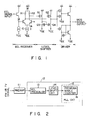
- Fig. 2 shows a circuit incorporating a level shift circuit according to an embodiment of the present invention.
- An FM signal or a TV signal is applied to preamplifier 11.
- the signal amplified by this preamplifier 11 is applied to LSI 12.
- LSI 12 is made up of prescaler 13 constructed with an ECL circuit, level shift circuit 14 for shifting an ECL level of the received signal into a CMOS logic level, and PLL circuit constructed with a CMOS circuit.
- the signal amplified by preamplifier 11 is supplied to ECL prescaler 13 in LSI 12.
- the output signal of this ECL prescaler 13 is supplied to level shift circuit 14.
- a signal in an ECL level e.g., with an amplitude of approximately 0.4V, for example, into a signal in a CMOS logic level, e.g., with an amplitude of approximately 4.4V.
- the output signal of level shift circuit 14 is supplied to programmable counter 16 formed in PLL circuit 15.
- Fig.3 for explaining a configuration of a level shift circuit according to an embodiment of the present invention, there are illustrated in detail the output stage of ECL prescaler 13, level shift circuit 14, and the input stage of programmable counter 16, which make up the circuit shown in Fig. 2.
- the output stage of ECL prescaler 13 contains a differential amplifier made up of resistors R3 and R4, NPN bipolar transistors T1 and T2, and constant current source 17. First ends of resistors R3 and R4 are coupled with power source Vcc, while the second ends of these resistors are respectively coupled with the collectors of bipolar transistors T1 and T2.
- the emitters of bipolar transistors T1 and T2 are connected together, and constant current source 17 is connected between the interconnection point and a ground point.
- Level shift circuit 14 is made up of capacitor (MOS capacitor) 19, CMOS inverter 20 made up of P and N channel MOS transistors Q5 and Q6, and a bias circuit for applying a bias voltage to the input node of CMOS inverter 20, and resistor R5 or a load element serving as a bias circuit for applying a bias voltage to the input node.
- a first electrode of capacitor 19 is connected to the collector of bipolar transistor T1.
- a second electrode of this capacitor 19 is connected to the input node of CMOS inverter 20.
- Resistor R5 is connected to between the input node and the output node of CMOS inverter 20.
- the output node of CMOS inverter 20 is connected the input stage of programmable counter (CMOS circuit) 16. In this instance, CMOS inverter 21 is used for that input stage.
- the output signal of ECL prescaler 13, which derived from the collector of transistor T1 has an amplitude of approximately 0.4V.
- this signal is applied to the first electrode of capacitor 19, it is applied to the second electrode of the capacitor through its capacitive coupling path, and in turn to the input node of CMOS inverter 20.
- Bias resistor R5 is connected between the input node and the output node of CMOS inverter 20, and provides a predetermined bias voltage to the input node.
- the ECL level signal which has been transferred through the capacitive coupling path, by CMOS inverter 20, the signal in an ECL level is converted into a signal in a CMOS logic level or of an amplitude of approximately of 4.4V.
- the level shifted signal is then supply to the input node of CMOS inverter 21 contained in the input stage of programmable counter 16.
- Fig.4 shows a relationship of input voltage V1 and output voltage V2 of the CMOS inverter 20 in the circuit shown in Fig. 3.
- Input voltage V1 is a potential formed by superposing the bias voltage generated across resistor R5 onto the output signal of ECL prescaler 13.
- the input voltage is a potential varying of an amplitude ⁇ V with respect to the bias voltage generated across resistor R5, in response to the output signal level of ECL prescaler 13.
- the voltage as the sum of voltage ⁇ V and bias voltage VR is set at a value near the circuit threshold voltage of CMOS inverter 20. Therefore, if the threshold voltage of MOS transistors Q5 and Q6 varies within a tolerable range due to the parameter variance caused in the manufacturing stage or the power voltage varies with a tolerable range, CMOS inverter 20 stably operates. Thus, the CMOS inverter is stable against the parameter variances and the power voltage variation. The fact that the CMOS inverter is stable against such situations implies that the production yield of the device will be improved.
- the ECL circuit and the CMOS inverter are coupled with each other so that the output signal of the ECL circuit is superposed on the bias voltage generated within the CMOS inverter.
- the capacitor shuts off the flow a DC-like voltage variation.
- Use of such a coupling capacitor ensures a stable operation of the CMOS inverter against the parameter variance and the power voltage variation, and consequently improves the production yield.
- the level shift circuit is made up of only capacitor 19, CMOS inverter 20 and the bias circuit or resistor R5.
- the level shifter in Fig. 3 requires a less number of circuit elements, and hence a less amount of current dissipation.
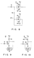
- CMOS inverter 20 To apply the input bias voltage to CMOS inverter 20, the embodiment shown in Fig. 3 uses resistor R5 connected between the input node and the output node of this CMOS inverter 20.
- a current path of N channel MOS transistor Q7 is connected between the input node and output node of CMOS inverter 20.
- Power voltage Vcc is applied to the gate of MOS transistor Q7, to set up a conduction state of the transistor.
- a modification as shown in Fig. 6 is also allowed.
- P channel MOS transistor Q8 is placed in the same place, with the gate being grounded for setting up a conduction state.
- Fig. 6 P channel MOS transistor Q8 is placed in the same place, with the gate being grounded for setting up a conduction state.
- the bias circuit is made up of N channel MOS transistor Q7 and P channel MOS transistor Q8.
- the current paths of these transistors are connected in parallel.
- the gates of transistors Q7 and Q8 are coupled with power source Vcc and a ground point, respectively.
- Fig. 8 shows another arrangement of the bias circuit for applying the bias voltage to the input node of CMOS inverter 20 in the circuit shown in Fig. 3.
- a first end of resistor R6 is connected to the input node of CMOS inverter 20.
- a second end of resistor R6 is connected to both the input and output nodes of CMOS inverter 22 containing P channel MOS transistor Q9 and N channel MOS transistor Q10.
- Bias circuit 23 is operable like the above bias circuits, and has the effects as those of the latter.
- CMOS inverter 20 While the above-mentioned embodiment employs CMOS inverter 20, other types of MOS inverter may of course be employed. Some specific examples of the MOS inverter are illustrated in Figs. 9 through 13.
- a MOS inverter is made up of current source 24 and N channel drive MOS transistor Q6.
- Bias circuit 25 is placed between the gate of MOS transistor Q6 and the output node.
- the bias circuit may be any of resistor R5 as shown in Fig. 3, MOS transistors Q7 and Q8 being set in a conductive state as shown in Figs. 5 and 6, and a transfer gate as shown in Fig. 7.
- the bias circuit may be replaced by the bias circuit 23 consisting of resistor R6 and MOS inverter 22, as shown in Fig. 8.
- MOS inverter thus arranged is substantially the same as CMOS inverter 20 in the basic operation, and the attained effects.
- constant current source 24 Some specific examples of constant current source 24 are illustrated in Figs. 10 to 13.
- the constant current source in Fig. 10 consists of N channel load MOS transistor Q11.
- the transistor is biased by voltage VB, to be in a conductive state.
- the example of Fig. 11 uses N channel load MOS transistor Q12 being conductive with its gate being biased by power voltage Vcc.
- the Fig. 12 example uses P channel load MOS transistor Q13 with the gate being connected to the output node for securing its conductive state.
- Resistor R7 may be used for the constant current source, as is shown in Fig. 13.
- the present invention has succeeded in providing a level shift circuit which is insensitive to the parameter variances caused in the manufacturing stage and the power voltage variation, and hence is stably operable, and has a good production yield. Additionally, a level shift circuit according to the present invention requires a simple circuit design for the output stage of the ECL circuit, and a less number of circuit elements, and a consequent reduction of current dissipation.
Abstract
Description
- The present invention relates to a level shift circuit, which is used for an FM frequency band prescaler in a radio receiver of the digital tuning type, for example, and shifts an output level of an ECL (Emitter Coupled Logic) into an input level of a CMOS (Complementary Metal Oxide Semiconductor) circuit.
- There has been known an ECL-CMOS level shift circuit of this type as shown in Fig. 1. The level shift circuit is described in "IEEE JOURNAL OF SOLID-STATE CIRCUITS, VOL. SC-21, NO. 5, OCTOBER 1986, 13-ns, 500-mW, 64Kbit, ECL RAM Using HI-BICMOS Technology" KATSUMI OGIUE et al., Fig. 6.
- To secure a normal operation of the circuit shown in Fig. 1, all of the MOS transistors Ql to Q4 making up a level shifter must operate in a saturation region. In an actual integrated circuit, however, those transistors Q1 to Q4 sometimes operate outside the saturation region due to a variance of circuit element parameters caused in the manufacturing stage, and a variation in the power voltage, and the like. When those transistors operate outside the saturation region, the level shift circuit operation is instable, and a production yield of the IC containing the level shift circuit is degraded. In designing the level shift circuit which is stable against the parameter variance and the power voltage variation, it is a key point how a voltage range of the gate bias voltage to amplifier (input) MOS transistors Ql and Q2 is set. The gate bias voltage range is determined depending on resistance of resistors R1 and R2 of the ECL receiver and current IA of constant
current source 10. The resistance and current IA also are inevitably influenced by the parameter variance and the power voltage variation. Thus, the character varying factors exist not only in the level shifter but also in the ECL receiver. This fact makes the design of the ECL receiver intricate and difficult. - Accordingly, an object of the present invention is to provide a level shift circuit which stably operates against the parameter variance and the power voltage variation, with a high production yield.
- Another object of the present invention is to provide a level shift circuit which allows an easy design of the output stage of an ECL circuit.
- A further object of the present invention is to provide a level shift circuit which requires a reduced number of circuit elements and a small power dissipation.
- According to one aspect of the present invention, there is provided a level shift circuit comprising a capacitor coupled at one electrode with an output stage of an ECL circuit, a MOS inverter connected at an input node to the other electrode of the capacitor and at an output node to an input stage of a CMOS circuit, and a bias circuit for applying a bias voltage to the input node of the MOS inverter.
- With such an arrangement, the ECL circuit is capacitively coupled with the CMOS circuit. Since the capacitor blocks flow of a voltage variation like DC, it blocks transfer of the DC like voltage variation due to the parameter variance and the power voltage variation. Further, since a bias voltage is applied to the input node of the MOS inverter, the output signal of the ECL circuit is superposed on the bias voltage and transferred to the input node of the MOS inverter. The bias voltage is set at a value near a circuit threshold voltage of the MOS inverter. Therefore, if the threshold voltage of the transistors making up the MOS inverter and the power voltage vary within a small range, the level shift circuit is stably operable.
- For the above reasons, the present invention provides a level shift circuit which stably operates against the parameter variance and the power voltage variation, with a high production yield. In designing the circuit, there is no need for allowing for the parameter variance and the power voltage variation. Accordingly, design of the output stage of the ECL circuit is easy. Since the capacitor and the MOS inverter make up the level shift circuit, the required number of circuit elements is smaller than that of the level shift circuit shown in Fig. 1, with a subsequent decrease of the power dissipation in the circuit.
- This invention can be more fully understood from the following detailed description when taken in conjunction with the accompanying drawings, in which:
- Fig. 1 is a circuit diagram showing a circuit for explaining a conventional ECL-CMOS level shift circuit;
- Fig. 2 is a block diagram showing a circuit to which a level shift circuit according to the present invention is applied;
- Fig. 3 is a circuit diagram showing a circuit for explaining a level shift circuit according to an embodiment of the present invention, the circuit made up of the output input stage of a programmable counter;
- Fig. 4 shows a graph showing an input voltage output voltage characteristic, which is for explaining the input/output characteristic of the MOS inverter in the level shift circuit shown in Fig. 3;
- Figs. 5 through 8 are circuit diagrams showing bias circuits each for applying a bias voltage to the input node of a MOS inverter in the circuit of Fig. 3; and
- Figs. 9 through 13 are circuit diagrams of other modifications of the MOS inverter in the circuit of Fig. 3.
- Fig. 2 shows a circuit incorporating a level shift circuit according to an embodiment of the present invention. An FM signal or a TV signal is applied to preamplifier 11. The signal amplified by this preamplifier 11 is applied to
LSI 12.LSI 12 is made up ofprescaler 13 constructed with an ECL circuit,level shift circuit 14 for shifting an ECL level of the received signal into a CMOS logic level, and PLL circuit constructed with a CMOS circuit. The signal amplified by preamplifier 11 is supplied toECL prescaler 13 inLSI 12. The output signal of thisECL prescaler 13 is supplied tolevel shift circuit 14. In this level shifter, a signal in an ECL level, e.g., with an amplitude of approximately 0.4V, for example, into a signal in a CMOS logic level, e.g., with an amplitude of approximately 4.4V. The output signal oflevel shift circuit 14 is supplied toprogrammable counter 16 formed inPLL circuit 15. - In Fig.3 for explaining a configuration of a level shift circuit according to an embodiment of the present invention, there are illustrated in detail the output stage of
ECL prescaler 13,level shift circuit 14, and the input stage ofprogrammable counter 16, which make up the circuit shown in Fig. 2. The output stage ofECL prescaler 13 contains a differential amplifier made up of resistors R3 and R4, NPN bipolar transistors T1 and T2, and constantcurrent source 17. First ends of resistors R3 and R4 are coupled with power source Vcc, while the second ends of these resistors are respectively coupled with the collectors of bipolar transistors T1 and T2. The emitters of bipolar transistors T1 and T2 are connected together, and constantcurrent source 17 is connected between the interconnection point and a ground point. The bases of bipolar transistors T1 and T2 are coupled for reception with the output signal ofinternal logic circuit 18.Level shift circuit 14 is made up of capacitor (MOS capacitor) 19,CMOS inverter 20 made up of P and N channel MOS transistors Q5 and Q6, and a bias circuit for applying a bias voltage to the input node ofCMOS inverter 20, and resistor R5 or a load element serving as a bias circuit for applying a bias voltage to the input node. A first electrode ofcapacitor 19 is connected to the collector of bipolar transistor T1. A second electrode of thiscapacitor 19 is connected to the input node ofCMOS inverter 20. Resistor R5 is connected to between the input node and the output node ofCMOS inverter 20. The output node ofCMOS inverter 20 is connected the input stage of programmable counter (CMOS circuit) 16. In this instance,CMOS inverter 21 is used for that input stage. - The operation of the circuit shown in Fig. 3 will be described. The output signal of
ECL prescaler 13, which derived from the collector of transistor T1, has an amplitude of approximately 0.4V. When this signal is applied to the first electrode ofcapacitor 19, it is applied to the second electrode of the capacitor through its capacitive coupling path, and in turn to the input node ofCMOS inverter 20. Bias resistor R5 is connected between the input node and the output node ofCMOS inverter 20, and provides a predetermined bias voltage to the input node. The ECL level signal, which has been transferred through the capacitive coupling path, byCMOS inverter 20, the signal in an ECL level is converted into a signal in a CMOS logic level or of an amplitude of approximately of 4.4V. The level shifted signal is then supply to the input node ofCMOS inverter 21 contained in the input stage ofprogrammable counter 16. - Fig.4 shows a relationship of input voltage V1 and output voltage V2 of the
CMOS inverter 20 in the circuit shown in Fig. 3. Input voltage V1 is a potential formed by superposing the bias voltage generated across resistor R5 onto the output signal ofECL prescaler 13. In other words, the input voltage is a potential varying of an amplitude Δ V with respect to the bias voltage generated across resistor R5, in response to the output signal level ofECL prescaler 13. The amplitude Δ V of the output signal ofECL prescaler 13 is expressed by the product "IB = R" of resistance R of resistor R3 and current IB flowing through constantcurrent source 17. The voltage as the sum of voltage Δ V and bias voltage VR is set at a value near the circuit threshold voltage ofCMOS inverter 20. Therefore, if the threshold voltage of MOS transistors Q5 and Q6 varies within a tolerable range due to the parameter variance caused in the manufacturing stage or the power voltage varies with a tolerable range,CMOS inverter 20 stably operates. Thus, the CMOS inverter is stable against the parameter variances and the power voltage variation. The fact that the CMOS inverter is stable against such situations implies that the production yield of the device will be improved. - The ECL circuit and the CMOS inverter are coupled with each other so that the output signal of the ECL circuit is superposed on the bias voltage generated within the CMOS inverter. With the nature of a capacitor to prohibit a DC like voltage variation from passing therethrough, the capacitor shuts off the flow a DC-like voltage variation. Use of such a coupling capacitor ensures a stable operation of the CMOS inverter against the parameter variance and the power voltage variation, and consequently improves the production yield. Thus, according to the present invention, in designing the output stage of the ECL circuit, there is no need for allowing for the parameter variance caused in the device manufacturing stage and the power voltage variation. In this respect, the circuit design is simplified. It is noted here that the level shift circuit is made up of
only capacitor 19,CMOS inverter 20 and the bias circuit or resistor R5. When comparing with the level shifter shown in Fig. 1, the level shifter in Fig. 3 requires a less number of circuit elements, and hence a less amount of current dissipation. - To apply the input bias voltage to
CMOS inverter 20, the embodiment shown in Fig. 3 uses resistor R5 connected between the input node and the output node of thisCMOS inverter 20. Alternatively, as shown in Fig. 5, a current path of N channel MOS transistor Q7 is connected between the input node and output node ofCMOS inverter 20. Power voltage Vcc is applied to the gate of MOS transistor Q7, to set up a conduction state of the transistor. A modification as shown in Fig. 6 is also allowed. As is shown in Fig. 6, P channel MOS transistor Q8 is placed in the same place, with the gate being grounded for setting up a conduction state. In Fig. 7, the bias circuit is made up of N channel MOS transistor Q7 and P channel MOS transistor Q8. The current paths of these transistors are connected in parallel. To render these transistors conductive, the gates of transistors Q7 and Q8 are coupled with power source Vcc and a ground point, respectively. - Fig. 8 shows another arrangement of the bias circuit for applying the bias voltage to the input node of
CMOS inverter 20 in the circuit shown in Fig. 3. In this bias circuit, a first end of resistor R6 is connected to the input node ofCMOS inverter 20. A second end of resistor R6 is connected to both the input and output nodes ofCMOS inverter 22 containing P channel MOS transistor Q9 and N channel MOS transistor Q10. Bias circuit 23 is operable like the above bias circuits, and has the effects as those of the latter. - While the above-mentioned embodiment employs
CMOS inverter 20, other types of MOS inverter may of course be employed. Some specific examples of the MOS inverter are illustrated in Figs. 9 through 13. In the example of Fig. 9, a MOS inverter is made up ofcurrent source 24 and N channel drive MOS transistor Q6.Bias circuit 25 is placed between the gate of MOS transistor Q6 and the output node. The bias circuit may be any of resistor R5 as shown in Fig. 3, MOS transistors Q7 and Q8 being set in a conductive state as shown in Figs. 5 and 6, and a transfer gate as shown in Fig. 7. The bias circuit may be replaced by the bias circuit 23 consisting of resistor R6 andMOS inverter 22, as shown in Fig. 8. - The MOS inverter thus arranged is substantially the same as
CMOS inverter 20 in the basic operation, and the attained effects. - Some specific examples of constant
current source 24 are illustrated in Figs. 10 to 13. The constant current source in Fig. 10 consists of N channel load MOS transistor Q11. The transistor is biased by voltage VB, to be in a conductive state. The example of Fig. 11 uses N channel load MOS transistor Q12 being conductive with its gate being biased by power voltage Vcc. The Fig. 12 example uses P channel load MOS transistor Q13 with the gate being connected to the output node for securing its conductive state. Resistor R7 may be used for the constant current source, as is shown in Fig. 13. - As seen from the foregoing description, the present invention has succeeded in providing a level shift circuit which is insensitive to the parameter variances caused in the manufacturing stage and the power voltage variation, and hence is stably operable, and has a good production yield. Additionally, a level shift circuit according to the present invention requires a simple circuit design for the output stage of the ECL circuit, and a less number of circuit elements, and a consequent reduction of current dissipation.
Claims (17)
Applications Claiming Priority (2)
| Application Number | Priority Date | Filing Date | Title |
|---|---|---|---|
| JP297961/87 | 1987-11-26 | ||
| JP62297961A JPH01138813A (en) | 1987-11-26 | 1987-11-26 | Level conversion circuit |
Publications (2)
| Publication Number | Publication Date |
|---|---|
| EP0318018A2 true EP0318018A2 (en) | 1989-05-31 |
| EP0318018A3 EP0318018A3 (en) | 1990-05-02 |
Family
ID=17853330
Family Applications (1)
| Application Number | Title | Priority Date | Filing Date |
|---|---|---|---|
| EP88119622A Withdrawn EP0318018A3 (en) | 1987-11-26 | 1988-11-24 | Level shift circuit for converting a signal in an ecl level into a signal in a CMOS logic level |
Country Status (4)
| Country | Link |
|---|---|
| US (1) | US4906871A (en) |
| EP (1) | EP0318018A3 (en) |
| JP (1) | JPH01138813A (en) |
| KR (1) | KR920003597B1 (en) |
Cited By (8)
| Publication number | Priority date | Publication date | Assignee | Title |
|---|---|---|---|---|
| EP0353508A2 (en) * | 1988-07-22 | 1990-02-07 | Siemens Aktiengesellschaft | ECL-MOS converter |
| EP0397335A2 (en) * | 1989-05-09 | 1990-11-14 | Advanced Micro Devices, Inc. | Complementary metal-oxide semiconductor translator |
| EP0438706A2 (en) * | 1990-01-26 | 1991-07-31 | International Business Machines Corporation | High speed cmos drive circuit |
| GB2328570A (en) * | 1997-08-20 | 1999-02-24 | Advantest Corp | Low amplitude CMOS logic signal transmission |
| EP0936526A2 (en) * | 1998-01-20 | 1999-08-18 | Siemens Aktiengesellschaft | Reference voltage generator |
| WO2001047111A2 (en) * | 1999-12-21 | 2001-06-28 | Teradyne, Inc. | Capacitively coupled re-referencing circuit with positive feedback |
| EP1164699A1 (en) * | 2000-06-14 | 2001-12-19 | Infineon Technologies AG | Logic level converting circuit |
| WO2002082636A2 (en) * | 2001-04-05 | 2002-10-17 | Koninklijke Philips Electronics N.V. | Data receiver gain enhancement |
Families Citing this family (35)
| Publication number | Priority date | Publication date | Assignee | Title |
|---|---|---|---|---|
| JPH0738580B2 (en) * | 1988-09-30 | 1995-04-26 | 日本電気株式会社 | Emitter-coupled logic circuit |
| US5051625B1 (en) * | 1988-10-28 | 1993-11-16 | Nissan Motor Co.,Ltd. | Output buffer circuits for reducing noise |
| DE3904901A1 (en) * | 1989-02-17 | 1990-08-23 | Texas Instruments Deutschland | INTEGRATED PULL-OUT LEVEL |
| US4968905A (en) * | 1989-08-25 | 1990-11-06 | Ncr Corporation | Temperature compensated high speed ECL-to-CMOS logic level translator |
| US5036226A (en) * | 1989-10-23 | 1991-07-30 | Ncr Corporation | Signal converting circuit |
| US5164616A (en) * | 1989-12-29 | 1992-11-17 | Xerox Corporation | Integrated sample and hold circuit with feedback circuit to increase storage time |
| US5038057A (en) * | 1990-05-29 | 1991-08-06 | Motorola, Inc. | ECL to CMOS logic translator |
| US5182473A (en) * | 1990-07-31 | 1993-01-26 | Cray Research, Inc. | Emitter emitter logic (EEL) and emitter collector dotted logic (ECDL) families |
| US5148059A (en) * | 1991-04-02 | 1992-09-15 | International Business Machines Corporation | CMOS and ECL logic circuit requiring no interface circuitry |
| US5254887A (en) * | 1991-06-27 | 1993-10-19 | Nec Corporation | ECL to BiCMIS level converter |
| KR940001816B1 (en) * | 1991-07-26 | 1994-03-09 | 삼성전자 주식회사 | Slew rate speed up circuit |
| US5202594A (en) * | 1992-02-04 | 1993-04-13 | Motorola, Inc. | Low power level converter |
| US5319252A (en) * | 1992-11-05 | 1994-06-07 | Xilinx, Inc. | Load programmable output buffer |
| JPH0746098A (en) * | 1993-08-03 | 1995-02-14 | Nec Corp | Delay circuit |
| US5682108A (en) * | 1995-05-17 | 1997-10-28 | Integrated Device Technology, Inc. | High speed level translator |
| CN1183587C (en) | 1996-04-08 | 2005-01-05 | 德克萨斯仪器股份有限公司 | Method and apparatus for galvanically isolating two integrated circuits from each others |
| US5754059A (en) * | 1997-01-14 | 1998-05-19 | International Business Machines Corporation | Multi-stage ECL-to-CMOS converter with wide dynamic range and high symmetry |
| US5973508A (en) * | 1997-05-21 | 1999-10-26 | International Business Machines Corp. | Voltage translation circuit for mixed voltage applications |
| US6252421B1 (en) * | 1998-07-27 | 2001-06-26 | Texas Instruments Incorporated | Differential, high speed, ECL to CMOS converter |
| JP3609977B2 (en) * | 1999-07-15 | 2005-01-12 | シャープ株式会社 | Level shift circuit and image display device |
| DE19949843C2 (en) * | 1999-10-15 | 2002-03-21 | Siemens Ag | Arrangement for level conversion of high-frequency low-voltage signals |
| JP3596540B2 (en) * | 2001-06-26 | 2004-12-02 | セイコーエプソン株式会社 | Level shifter and electro-optical device using the same |
| US6507220B1 (en) * | 2001-09-28 | 2003-01-14 | Xilinx, Inc. | Correction of duty-cycle distortion in communications and other circuits |
| KR100487947B1 (en) * | 2002-11-22 | 2005-05-06 | 삼성전자주식회사 | Clock squarer |
| US7176720B1 (en) * | 2003-03-14 | 2007-02-13 | Cypress Semiconductor Corp. | Low duty cycle distortion differential to CMOS translator |
| JP2005266043A (en) * | 2004-03-17 | 2005-09-29 | Hitachi Displays Ltd | Image display panel and level shift circuit |
| US7064598B2 (en) * | 2004-03-25 | 2006-06-20 | Silicon Laboratories, Inc. | Radio frequency CMOS buffer circuit and method |
| JP4560552B2 (en) * | 2004-12-30 | 2010-10-13 | エージェンシー フォー サイエンス,テクノロジー アンド リサーチ | Fully integrated ultra wideband transmitter circuit and system |
| TW200715092A (en) * | 2005-10-06 | 2007-04-16 | Denmos Technology Inc | Current bias circuit and current bias start-up circuit thereof |
| JP2007259122A (en) * | 2006-03-23 | 2007-10-04 | Renesas Technology Corp | Semiconductor integrated circuit for communication |
| US8729954B2 (en) * | 2011-08-31 | 2014-05-20 | Freescale Semiconductor, Inc. | MOFSET mismatch characterization circuit |
| US9111894B2 (en) | 2011-08-31 | 2015-08-18 | Freescale Semiconductor, Inc. | MOFSET mismatch characterization circuit |
| US9270273B2 (en) * | 2011-10-28 | 2016-02-23 | Texas Instruments Incorporated | Level shifter |
| US8680901B2 (en) * | 2012-08-06 | 2014-03-25 | Texas Instruments Incorporated | Power on reset generation circuits in integrated circuits |
| US9312858B2 (en) | 2014-06-02 | 2016-04-12 | International Business Machines Corporation | Level shifter for a time-varying input |
Citations (3)
| Publication number | Priority date | Publication date | Assignee | Title |
|---|---|---|---|---|
| EP0142167A2 (en) * | 1983-11-14 | 1985-05-22 | Nec Corporation | Level shifting circuit |
| US4645951A (en) * | 1983-08-31 | 1987-02-24 | Hitachi, Ltd. | Semiconductor integrated circuit having a C-MOS internal logic block and an output buffer for providing ECL level signals |
| EP0218747A1 (en) * | 1985-10-15 | 1987-04-22 | International Business Machines Corporation | Sense amplifier for amplifying signals on a biased line |
Family Cites Families (8)
| Publication number | Priority date | Publication date | Assignee | Title |
|---|---|---|---|---|
| US4029971A (en) * | 1976-02-13 | 1977-06-14 | Rca Corporation | Tri-state logic circuit |
| GB1564671A (en) * | 1978-04-12 | 1980-04-10 | Hughes Microelectronics Ltd | Comparator |
| DE3360366D1 (en) * | 1982-02-26 | 1985-08-14 | Toshiba Kk | Mos switch circuit |
| JPH0773205B2 (en) * | 1983-12-20 | 1995-08-02 | 株式会社日立製作所 | Level conversion circuit |
| JPS60194614A (en) * | 1984-03-16 | 1985-10-03 | Hitachi Ltd | Interface circuit |
| JPS6119226A (en) * | 1984-07-05 | 1986-01-28 | Hitachi Ltd | Level converting circuit |
| US4703198A (en) * | 1986-07-07 | 1987-10-27 | Ford Motor Company | Bi-directional data transfer circuit that is directionally responsive to the impedance condition of an associated input/output port of a microcomputer |
| US4754165A (en) * | 1986-07-29 | 1988-06-28 | Hewlett-Packard Company | Static MOS super buffer latch |
-
1987
- 1987-11-26 JP JP62297961A patent/JPH01138813A/en active Pending
-
1988
- 1988-11-22 KR KR1019880015349A patent/KR920003597B1/en not_active IP Right Cessation
- 1988-11-24 EP EP88119622A patent/EP0318018A3/en not_active Withdrawn
- 1988-11-25 US US07/275,867 patent/US4906871A/en not_active Expired - Lifetime
Patent Citations (3)
| Publication number | Priority date | Publication date | Assignee | Title |
|---|---|---|---|---|
| US4645951A (en) * | 1983-08-31 | 1987-02-24 | Hitachi, Ltd. | Semiconductor integrated circuit having a C-MOS internal logic block and an output buffer for providing ECL level signals |
| EP0142167A2 (en) * | 1983-11-14 | 1985-05-22 | Nec Corporation | Level shifting circuit |
| EP0218747A1 (en) * | 1985-10-15 | 1987-04-22 | International Business Machines Corporation | Sense amplifier for amplifying signals on a biased line |
Non-Patent Citations (1)
| Title |
|---|
| P.R. GRAY et al.: "ANALYSIS AND DESIGN OF ANALOG INTEGRATED CIRCUITS", 2nd edition, 1984, pages 145-148, JOHN WILEY & SONS, New York, US; * |
Cited By (18)
| Publication number | Priority date | Publication date | Assignee | Title |
|---|---|---|---|---|
| EP0353508A2 (en) * | 1988-07-22 | 1990-02-07 | Siemens Aktiengesellschaft | ECL-MOS converter |
| EP0353508A3 (en) * | 1988-07-22 | 1990-05-16 | Siemens Aktiengesellschaft | Ecl-mos converter |
| EP0397335A2 (en) * | 1989-05-09 | 1990-11-14 | Advanced Micro Devices, Inc. | Complementary metal-oxide semiconductor translator |
| EP0397335A3 (en) * | 1989-05-09 | 1991-05-29 | Advanced Micro Devices, Inc. | Complementary metal-oxide semiconductor translator |
| EP0438706A2 (en) * | 1990-01-26 | 1991-07-31 | International Business Machines Corporation | High speed cmos drive circuit |
| EP0438706A3 (en) * | 1990-01-26 | 1992-01-29 | International Business Machines Corporation | High speed cmos drive circuit |
| US6166575A (en) * | 1997-08-20 | 2000-12-26 | Advantest Corporation | Signal transmission circuit achieving significantly improved response time of a driven circuit, CMOS semiconductor device and circuit board therefor |
| GB2328570A (en) * | 1997-08-20 | 1999-02-24 | Advantest Corp | Low amplitude CMOS logic signal transmission |
| GB2328570B (en) * | 1997-08-20 | 2001-07-04 | Advantest Corp | Signal transmission circuit,cmos semiconductor device,and circuit board |
| US6313677B1 (en) | 1997-08-20 | 2001-11-06 | Advantest Corporation | Signal transmission circuit, CMOS semiconductor device, and circuit board |
| KR100452912B1 (en) * | 1997-08-20 | 2005-05-13 | 가부시키가이샤 아드반테스트 | Signal transmission circuit, cmos semiconductor device, and circuit board |
| EP0936526A2 (en) * | 1998-01-20 | 1999-08-18 | Siemens Aktiengesellschaft | Reference voltage generator |
| EP0936526A3 (en) * | 1998-01-20 | 2001-10-17 | Siemens Aktiengesellschaft | Reference voltage generator |
| WO2001047111A2 (en) * | 1999-12-21 | 2001-06-28 | Teradyne, Inc. | Capacitively coupled re-referencing circuit with positive feedback |
| WO2001047111A3 (en) * | 1999-12-21 | 2002-02-14 | Teradyne Inc | Capacitively coupled re-referencing circuit with positive feedback |
| EP1164699A1 (en) * | 2000-06-14 | 2001-12-19 | Infineon Technologies AG | Logic level converting circuit |
| WO2002082636A2 (en) * | 2001-04-05 | 2002-10-17 | Koninklijke Philips Electronics N.V. | Data receiver gain enhancement |
| WO2002082636A3 (en) * | 2001-04-05 | 2004-07-29 | Koninkl Philips Electronics Nv | Data receiver gain enhancement |
Also Published As
| Publication number | Publication date |
|---|---|
| JPH01138813A (en) | 1989-05-31 |
| KR890009068A (en) | 1989-07-15 |
| EP0318018A3 (en) | 1990-05-02 |
| KR920003597B1 (en) | 1992-05-04 |
| US4906871A (en) | 1990-03-06 |
Similar Documents
| Publication | Publication Date | Title |
|---|---|---|
| EP0318018A2 (en) | Level shift circuit for converting a signal in an ecl level into a signal in a CMOS logic level | |
| JPH0119294B2 (en) | ||
| US5365127A (en) | Circuit for conversion from CMOS voltage levels to shifted ECL voltage levels with process compensation | |
| US3816765A (en) | Digital interface circuit for a random noise generator | |
| EP0293833A2 (en) | Output circuit having wide range frequency response characteristic | |
| US5994744A (en) | Analog switching circuit | |
| US4357548A (en) | Circuit arrangement using emitter coupled logic and integrated injection logic | |
| US4607177A (en) | Circuit arrangement for conversion TTL logic signals to ECL logic signals | |
| JPH0645878A (en) | Perfect differential relaxation-type voltage-controlled transmitter and its method | |
| US4620115A (en) | Voltage-temperature compensated threshold for hysteresis line receiver at TTL supply voltage | |
| EP0417786B1 (en) | A level shift circuit for achieving a high-speed processing and an improved output current capability | |
| JPH05291887A (en) | Schmitt trigger circuit | |
| JPH114164A (en) | Charge pump circuit where use of frequency synthesizer in frequency control loop is intended, integrated circuit and radio wave receiver | |
| US3509362A (en) | Switching circuit | |
| EP1137184A1 (en) | Voltage level shifting circuit | |
| US4383224A (en) | NMOS Crystal oscillator | |
| JPH09130218A (en) | Operational amplifier and digital signal transmission circuit | |
| JP2728013B2 (en) | BiCMOS logic gate circuit | |
| EP0266112B1 (en) | Cml bias generator | |
| JPH1155145A (en) | Integrated circuit for transmitter-receiver | |
| US4771190A (en) | Emitter coupled logic circuit provided with pull-down resistors at respective bases of input transistors | |
| US5066876A (en) | Circuit for converting ecl level signals to mos level signals | |
| US4996499A (en) | Amplitude stabilized oscillator amplifier | |
| KR100247367B1 (en) | Voltage controlled oscillator | |
| US5945843A (en) | Semiconductor integrated circuit |
Legal Events
| Date | Code | Title | Description |
|---|---|---|---|
| PUAI | Public reference made under article 153(3) epc to a published international application that has entered the european phase |
Free format text: ORIGINAL CODE: 0009012 |
|
| 17P | Request for examination filed |
Effective date: 19881221 |
|
| AK | Designated contracting states |
Kind code of ref document: A2 Designated state(s): DE FR GB |
|
| PUAL | Search report despatched |
Free format text: ORIGINAL CODE: 0009013 |
|
| AK | Designated contracting states |
Kind code of ref document: A3 Designated state(s): DE FR GB |
|
| 17Q | First examination report despatched |
Effective date: 19911206 |
|
| STAA | Information on the status of an ep patent application or granted ep patent |
Free format text: STATUS: THE APPLICATION IS DEEMED TO BE WITHDRAWN |
|
| 18D | Application deemed to be withdrawn |
Effective date: 19930921 |