EP0314277A2 - Simd array processor - Google Patents
Simd array processor Download PDFInfo
- Publication number
- EP0314277A2 EP0314277A2 EP88307885A EP88307885A EP0314277A2 EP 0314277 A2 EP0314277 A2 EP 0314277A2 EP 88307885 A EP88307885 A EP 88307885A EP 88307885 A EP88307885 A EP 88307885A EP 0314277 A2 EP0314277 A2 EP 0314277A2
- Authority
- EP
- European Patent Office
- Prior art keywords
- array
- global
- programmable
- instruction
- data
- Prior art date
- Legal status (The legal status is an assumption and is not a legal conclusion. Google has not performed a legal analysis and makes no representation as to the accuracy of the status listed.)
- Granted
Links
- 238000012545 processing Methods 0.000 claims abstract description 141
- 238000012986 modification Methods 0.000 claims abstract description 27
- 230000004048 modification Effects 0.000 claims abstract description 27
- 238000003860 storage Methods 0.000 claims abstract description 17
- 230000004044 response Effects 0.000 claims abstract description 8
- 230000001419 dependent effect Effects 0.000 claims 1
- 238000012546 transfer Methods 0.000 abstract description 2
- 238000004422 calculation algorithm Methods 0.000 description 25
- 230000002457 bidirectional effect Effects 0.000 description 8
- 238000010586 diagram Methods 0.000 description 8
- 230000006870 function Effects 0.000 description 3
- 230000001154 acute effect Effects 0.000 description 2
- 230000008859 change Effects 0.000 description 2
- 229910052729 chemical element Inorganic materials 0.000 description 2
- 239000011159 matrix material Substances 0.000 description 2
- 238000000034 method Methods 0.000 description 2
- 239000003607 modifier Substances 0.000 description 2
- 230000008569 process Effects 0.000 description 2
- 238000012163 sequencing technique Methods 0.000 description 2
- 238000012360 testing method Methods 0.000 description 2
- 238000004364 calculation method Methods 0.000 description 1
- 230000014759 maintenance of location Effects 0.000 description 1
- 238000013507 mapping Methods 0.000 description 1
- 238000002360 preparation method Methods 0.000 description 1
Images


Classifications
-
- G—PHYSICS
- G06—COMPUTING; CALCULATING OR COUNTING
- G06F—ELECTRIC DIGITAL DATA PROCESSING
- G06F9/00—Arrangements for program control, e.g. control units
- G06F9/06—Arrangements for program control, e.g. control units using stored programs, i.e. using an internal store of processing equipment to receive or retain programs
- G06F9/30—Arrangements for executing machine instructions, e.g. instruction decode
- G06F9/38—Concurrent instruction execution, e.g. pipeline, look ahead
- G06F9/3885—Concurrent instruction execution, e.g. pipeline, look ahead using a plurality of independent parallel functional units
-
- G—PHYSICS
- G06—COMPUTING; CALCULATING OR COUNTING
- G06F—ELECTRIC DIGITAL DATA PROCESSING
- G06F15/00—Digital computers in general; Data processing equipment in general
- G06F15/76—Architectures of general purpose stored program computers
- G06F15/80—Architectures of general purpose stored program computers comprising an array of processing units with common control, e.g. single instruction multiple data processors
- G06F15/8007—Architectures of general purpose stored program computers comprising an array of processing units with common control, e.g. single instruction multiple data processors single instruction multiple data [SIMD] multiprocessors
- G06F15/8023—Two dimensional arrays, e.g. mesh, torus
-
- G—PHYSICS
- G06—COMPUTING; CALCULATING OR COUNTING
- G06F—ELECTRIC DIGITAL DATA PROCESSING
- G06F9/00—Arrangements for program control, e.g. control units
- G06F9/06—Arrangements for program control, e.g. control units using stored programs, i.e. using an internal store of processing equipment to receive or retain programs
- G06F9/30—Arrangements for executing machine instructions, e.g. instruction decode
- G06F9/30181—Instruction operation extension or modification
- G06F9/30196—Instruction operation extension or modification using decoder, e.g. decoder per instruction set, adaptable or programmable decoders
-
- G—PHYSICS
- G06—COMPUTING; CALCULATING OR COUNTING
- G06F—ELECTRIC DIGITAL DATA PROCESSING
- G06F9/00—Arrangements for program control, e.g. control units
- G06F9/06—Arrangements for program control, e.g. control units using stored programs, i.e. using an internal store of processing equipment to receive or retain programs
- G06F9/30—Arrangements for executing machine instructions, e.g. instruction decode
- G06F9/38—Concurrent instruction execution, e.g. pipeline, look ahead
- G06F9/3885—Concurrent instruction execution, e.g. pipeline, look ahead using a plurality of independent parallel functional units
- G06F9/3887—Concurrent instruction execution, e.g. pipeline, look ahead using a plurality of independent parallel functional units controlled by a single instruction for multiple data lanes [SIMD]
Definitions
- the present invention relates to a single-instruction-multiple-data (SIMD) array processor comprising a multidimensional array of interconnected processors.
- SIMD single-instruction-multiple-data
- MIMD multiple-instruction-multiple-data
- SIMD single-instruction- multiple-data
- MIMD array processor each of the processing elements in the array executes its own unique instruction stream with its own data.
- an array processor of the type to which the present invention is directed that is a SIMD array processor, in that the individual processing elements operate instead under the control of a common, or global instruction stream from a single control unit.
- a SIMD machine is less flexible and can execute a more limited range of functions in parallel than a MIMD machine.
- the parallel processing elements of a SIMD machine are typically simpler and more numerous than in a MIMD processor.
- SIMD array processors consist of a two dimensional array of processing elements, each processing element being connected to its nearest neighbours to form a so-called NEWS (North, East, West, South) network.
- array processors of this type are the ICL Distriheaded Array Processor (DAP), and the "Connection Machine” which are described in “Parallel Computers” by Hockney & Jesshope, Adam Hilger Ltd. 1981, pp 182-184 and "The Connection Machine” by W. Daniel Hillis, MIT Press 1986, pp 74-76 respectively.
- UK -A- 1445714 is also illustrative of a prior art SIMD array processor.
- the object of the present invention is to provide a SIMD array processor comprising a multi-dimensional array of processing elements which has an enhanced degree of flexibility to enable the potential for parallel processing to be better exploited without resorting to the expense and complexity of a MIMD processor.
- a SIMD array processor comprising a multi-dimensional array of processing elements and control logic for issuing global instructions to said array, characterised in that a processing element includes programmable decoding means for the individual decoding for execution by that processing element of a global instruction, the programmable decoding means of respective processing elements being programmable in response to a global load instruction from the control logic.
- the programmable decoding means comprises programmable modifying means for locally modifying selected bits of the global instruction to form locally modified bits and fixed decoding means for decoding bits of the global instruction as received and said locally modified bits.
- the processing elements in the array are each associated with storage for control information and data and, in response to a global load instruction, the fixed decoding means in a processing element causes modification information to be loaded from selected locations in said storage into the programmable modifying means of that processing element, whereby the programmable modifying means of respective processing elements may be programmed.
- the processing elements in that embodiment are each associated with a corresponding block of said storage for control information and data and means are provided for the control logic to access said storage for storing appropriate modification information for the programmable decoding means in corresponding locations in each said block of storage.
- the programmable modifying means comprises a look-up table having a serial write port for receiving said modification information serially from storage and a parallel read port for receiving said selected bits of a global instruction in parallel.
- the programmable decoding means are adapted to be programmed to locally modify a global shift instruction, whereby data distributed throughout the array may be shifted at one time in a plurality of locally determined directions within the array.
- the processing elements in this processor are interconnected in a plurality of orthogonal directions. Each processing element comprises a plurality of output registers and a multi-way input multiplexer such that multiple simultaneous shift operations can be performed in each of a plurality of orthogonal directions by a processing element.
- SIMD array processor in accordance with the present invention gives rise to a family of algorithms which it has not been possible to perform in parallel on prior SIMD array processors. Some of these are described later.
- a SIMD array processor in accordance with the present invention is particularly suitable for image processing applications and accordingly it may be implemented as part of a display system.
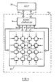
- FIG. 1 illustrates a typical structure for a SIMD array processor 10.
- the processor 10 comprises an array 12 of processing elements P(i,j), and an array controller 14 for issuing a stream of global instructions to the processing elements P(i,j).
- Each of the processing elements operates on a single bit at any one time and has associated therewith a block of storage (not shown).
- the processing elements are connected by a so called NEWS (North, East, West, South) network to their respective neighbours by bidirectional bit lines.
- NEWS North, East, West, South
- processing element P(i,j) is connected to the processing elements P(i-1,j), P(i,j+1) P(i,j-1) and P(i+1,j) in the Northern, Eastern, Western and Southern directions respectively.
- the NEWS network is also connected toroidally at its edges so that the Northern and Southern edges are bidirectionally interconnected and the Western and Eastern edges are similarly interconnected.
- a controller-array data bus 26 is connected to the NEWS network. As shown it is connected to the East-West boundary of the array. It could equally be connected instead, or additionally, to the North-South boundary, or indeed to each processing element. It is connected to the East-West boundary by means of bidirectional tristate drivers which are connected to the toroidal East-West NEWS connections. It will be apparent to the skilled person that this is only one of many possible means of connection of the data bus 26.
- the number of processing elements in the array can be chosen as required.
- a typical number, as is used in a specific embodiment of the present invention to be described later, is 32 X 32 1024 individual processing elements.
- 16 individual processing elements are shown.
- Figure 1 a double line connecting functional elements is used to represent a plurality of connection lines or a bus, a single line indicates a single bit line.
- the lines may be uni- or bidirectional as appropriate as indicated by the arrows in the Figures.
- the array controller issues instructions in parallel to the processing elements via an instruction bus 18 and issues row select and column select signals via row select lines 20 and column select lines 22, respectively. These instructions cause the processing elements to load data from storage, to process the data and then to store the data once more in storage.
- Each processing element has access to a bit slice of main memory.
- the main memory of the array processor is separativelyed into 1024 slices for a 1024 processing element array. This means that up to thirty two 32-bit words can be transferred in or out of storage at one time.
- the memory is addressed in terms of an index address which is supplied to the memory address lines via an address bus 24 and a read or write instruction is supplied to each of the processing elements in parallel.
- the row and column select signals on the row and column select lines identify which of the processing elements are to perform the operation.
- a host processor 28 is also shown in Figure 1. This processor is used to load microcode programs into the array controller 14, to exchange data with it and to monitor its status via a host-controller data bus 30 and an address and control bus 31.
- the host processor can be any suitable general purpose computer such as a mainframe computer or a personal computer. No further description of the host processor is necessary as this does not form part of the present invention.
- SIMD array processor in accordance with the present invention, which also has the overall structure shown in Figure 1, will be described. It will be apparent from the following, however, that the present invention is not limited to the structure illustrated in Figure 1.
- the array of processors could be organised on a 3-D, 4-D (using clusters), etc basis rather than on a 2-D basis.
- a SIMD array processor in accordance with the present invention may form an integral part of, for example, a display system such as a workstation with a display adapter.
- a SIMD array processor in accordance with the present invention is particularly suitable for image processing applications.
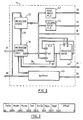
- Figure 2 illustrates how the array controller shown in Figure 1 is structured in the specific embodiment of a SIMD array processor in accordance with the present invention. Neither the detailed structure of the array controller shown in Figure 2, nor specific details of its operation are essential to the present invention. Consequently, the structure and operation of the controller will only be briefly described in the following.
- the array controller 14 comprises a microcode store 32 into which microcode defining the processing to be performed by the array processor is loaded by the host 28 using the data bus 30 and the address and control bus 31. Once the operation of the array controller 14 has been initiated by the host 28, the sequencing of the microcode is controlled by the microcode control unit 34 which is connected to the microcode store by bus 36.
- An ALU 38 and register bank 40 are used in the generation of array memory addresses which are output on the address bus 24, loop counting, jump address calculation and miscellaneous general purpose register operations.
- a flag line 39 is provided for conditional branching.
- a row mask PLA (Programmed Logic Array) 42 and a column mask PLA 44 are used for decoding row and column mask codes in a microinstruction being executed to generate signals on individual row select lines 20 and column select lines 22. Operation codes forming the instructions to the processing elements P(i,j) are fed onto the instruction bus 18.
- a data buffer 46 is shown between the host-controller data bus 30 and the controller-array data bus 26. This allows data from the host which is to be written into the array of processors to be rapidly down-loaded into the array controller 14. The data can then be loaded, under control of the microcode, into the array of processors. Similarly, the buffer can be used for transferring data between the array and the host. For this purpose the buffer is arranged as a bidirectional FIFO buffer under control of the microcode control unit.
- FIG. 3 The instruction format used in the specific embodiment of the present invention is illustrated in Figure 3. It should be noted that the format shown in Figure 3 is merely that used in the specific example of a SIMD array processor described herein. In other embodiments of the invention another format might well be used depending on the form of the controller for the processor array, the complexity of the individual processing elements and so on as will be apparent from the following description to one skilled in the art.
- the fields of the instruction which relate to the control of the processor array are the processing element operation code "PeOP", bits 63 to 56, the row mask code “Maskr”, bits 55 to 48, and the column mask code “Maskc”, bits 47 to 40.
- the "PeOP” field forms the operation code, or instruction, which is issued globally in parallel to processing elements in the array.
- the purpose of the row and column masks is to enable the instruction specified by the "PeOP" code to be executed by selected processing elements only. This enables memory read operations, inter-processor element shifts and intra-processor element register operations to be performed by selected processing elements only.
- the contents of the "Maskr" and “Maskc” fields are decoded by the row mask PLA 42 and the column mask PLA 44, respectively, for setting appropriate individual row select lines 20 and column select lines 22.
- the further fields shown in Figure 3 are all concerned with the sequencing of the array controller and array memory address generation in a conventional manner.
- the "Test” field, bits 39 to 36, defines the instruction flow within the array controller and is fed to "test” input of the microcode control unit, so that jumps, etc. are possible.
- the field “Aluop”, bits 35 to 32, defines the general operation of the controller ALU 38 and is fed to its Fsel input.
- the fields "Regs”, bits 31 to 28, and “Regd”, bits 27 to 24, are used for selecting source and destination registers in the controller's register bank 40 and are fed for this purpose to R and W control inputs, respectively, of the register bank.
- bits 23 to 0 defines an argument for ALU operation and array memory address generation and is fed to the input A of the ALU 38.
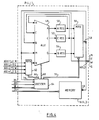
- FIG. 4 illustrates the principle components of one of the individual processing elements P(i,j) from the processor array 12. It should be understood that each processing element operates on a single bit of data at a time.
- the processing element comprises an ALU 48, which in the specific example of a processing element shown, comprises inputs labelled A, C, Q, M, and N and outputs A,C and Q.
- the outputs A, C, and Q are connected to an A, or result register 50, a C, or carry register 52 and a Q, or NEWS output register 54, each of which is able to store a single bit of information.
- the outputs of these registers are connected back to the corresponding A, C and Q inputs to the ALU and also to a multiplexer 56.
- the multiplexer 56 enables the output of a selectable one of the A, C and Q registers to be passed to its output 58.
- the output 58 of the multiplexer 56 is connected to the M input of the ALU and also to bidirectional data port 59 of the slice of memory 16(i,j) associated with the processing element P(i,j).
- Each processing element is associated with a slice, or block, of memory 16(i,j) one bit wide. Although this slice or block memory is logically included within the processing element it may in fact be physically separate therefrom.
- the 32 X 32 blocks of memory of the array can be thought of as an array memory, comprising a plurality of planes, each of which comprises 32 32-bit words. Each plane comprises a bit from each of the processing elements at a corresponding index address. By supplying a single index address to the array memory via the address bus 24, one of the planes of bits can be accessed.
- the output of the Q register also forms the NEWS output 60(i,j) of the processing element P(i,j) which is connected to the adjacent processing elements in the North (P(i-1,j)), East (P(i,j+1)), West P(i,j-1)) and South (P(i+1,j)) directions.
- Data to be shifted into the processing element P(i,j) from an adjacent element in the NEWS network is selected by means of an input multiplexer 62 which is connected to the NEWS outputs 60 (i-1,j), 60(i,j+1), 60(i,j-1) and 60(i+1,j) of the adjacent processing elements in the North, East, West and South directions respectively.
- the output of the input multiplexer 62 is connected to the N input of the ALU 48.
- the operation of the processing element is controlled by instructions, or operation codes, received from the array controller 14 over the instruction bus 18.
- the operation codes "PeOP" from the array controller are received in parallel on the instruction bus 18 from the array controller at the decoder 64 in each of the processing elements.
- the status of the row and column select lines 20i and 22j for the processing element in question will determine whether the instruction is performed by that processing element or not.
- the decoder in each processing element is connected to the column and row select lines appropriate for the position of the processing element in the array. For the processing element P(i,j) on the ith row and the jth column this will be the ith row select line 20i and jth column select line 22j.
- the decoder When both the row and the column select lines to a particular decoder 64 are selected, the decoder will decode the received operation code and thereby cause the processor to carry out the specified instruction by issuing control signals over control buses 66, 68 and 70 to the input multiplexer 62, the ALU 48 and the output multiplexer 56.
- the first type of operation is a routing operation in which a bit of input data is simply passed from the input of the ALU to the output. For example, a bit of data can be passed from a selected one of the NEWS inputs to the multiplexer 62 via that input multiplexer 62, the input N of the ALU and the Q output of the ALU to the Q register 54 which forms the NEWS output register. From there the information is output onto the NEWS network. Similarly a bit of data can be routed from a location in memory 16 specified by an address on the memory address bus 24 via the bidirectional data port 59 of the memory, the M input and the Q output of the ALU to the Q register.
- a second basic type of operation is an arithmetic one.
- the result register 50 and the carry register 52 are used principally for such operations.
- the actual operations which can be performed by the ALU will depend on the internal structure of the unit. This will not be described in detail as it is not essential to an understanding of the present invention.
- the ALU is implemented in a conventional manner as will be evident to one skilled in the art.
- the decoder has been hard-wired, usually in the form of a plurality of hard-wired logic gates.
- the decoder in a SIMD array processor in accordance with the present invention is, in contrast, programmable.
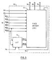
- the decoder is programmable by the provision of a look-up table which operates as an instruction modifier. Further, in this embodiment of the invention, only selected bits of the operation code input to the decoder 64 are modified by the look-up table.
- Figure 5 illustrates the decoder 64 of this specific embodiment of the present invention in more detail. It comprises a first part 72 in the form of conventional fixed decoder logic such as hard-wired gates and a second, programmable part in the form of a look-up table (LUT) 74.
- the bits of the operation code on lines 18(i) to 18(vi) and the row and column select lines are input directly to the PLA as usual, but two of the bits 18(v) and 18(vi) of the operation code are also used to address the look-up table in parallel.
- the two-bit output of the look-up table location accessed by these bits forms modified operation bit lines 18(vii) and 18(viii) which are also input to the fixed decoder logic 72.
- the fixed decoder logic 72 logically combines the input data on lines 18(i)-(viii) to form the output control information on the control buses 66, 68 and 70.
- the look-up table shown in Figure 5 comprises four words of two bits each. These eight bits of data are loaded in series over a data line 76 from memory 16(i,j) (see also Figure 4) in response to global "load look-up table" instruction from the array controller. As the look-up tables of the processing elements will contain indeterminate information before being initialised, the "load look-up table” instruction only uses unmodified bits 18(i) to (vi) of the operation code as received , that is the bits that do not go through the look-up table.
- the decoder in each of the processing elements produces the control signals on the buses 66, 68, 70 and on the control line 78 internal to the decoder when this instruction is received irrespective of the value of the lines 18(v) and 18(vi).
- the control line 78 is a write enable line for the look-up table.
- Appropriate control, or modification, data for the look-up table of each of the respective processing elements would have been previously loaded via the data bus 26 and the Q register 54 into corresponding locations in the slice of memory 16(i,j) associated with each processing element P(i,j) so that the control data may be accessed and read into the look-up tables of each of the processing elements using global instructions and memory addresses.
- the storing of the control information is carried out by operating the array in a prior art manner using global unmodified instructions.
- a SIMD array processor there are essentially two sorts of global instructions defined by the "PeOP" operation codes. These are global instructions which cannot be modified locally and global instructions which can be modified locally.
- the first sort are global instructions which are used for initially loading data into the processor array, for shifting the data through the array for storing that data in the array memory and for subsequently loading modification data into the look-up tables. All other instructions can, in principle be modified locally, but they can only be used when appropriate modification information has been loaded into the look-up tables.
- the fixed decoder logic 72 logically combines the input data on lines 18(i) to 18(vi) (ie the unmodified instruction bits) in such a manner that it recognises whether the instruction being decoded is locally modifiable and whether the input data on lines 18(vii) and 18(viii) (ie the modified instruction bits) are to be used to determine the operation actually performed by the processing element.
- the programmable decoder is used to specify a different shift direction for different processing elements despite the restriction of the global instructions.
- the actual direction in which data is shifted is the result of the selection of one of the NEWS inputs to the input multiplexer 62.
- two bits of the instruction code eg. the bits 18(v) and 18(vi)
- a look-up table for local modification of those two bits means that it is possible to individually specify a local direction of shift in each processing element in response to a given global shift instruction.
- Successive 32-bit words of data are read into the Western edge of the array of processors via the bidirectional tri-state drivers in the toroidal East-West NEWS connections and are shifted across the array using global unmodified shift East instructions.
- respective bits of the first 32 words of data are written into corresponding memory locations in the blocks of memory associated with each processing element using a global unmodified write instruction. These steps are repeated until all the necessary information has been loaded into memory.
- modification data is read into the look-up tables of the processing elements using a global unmodified "load look-up table" instruction. Once this step has been performed, the array of processors can be used to perform algorithms using locally modifiable instructions.
- a SIMD array processor in accordance with the present invention is particularly suitable for image processing applications.
- a high bandwidth data bus could additionally be connected to the processor array of a SIMD array processor in accordance with the present invention.
- Data could be input to the array from a video camera or video store and output to a video store or video display device via such a high bandwidth bus instead of over the controller-array data bus 26.
- the high bandwidth data bus could be connected to the array in a similar manner to the controller-array data bus.
- a separate video input (not shown) to the input multiplexer 62 and a separate video output register (not shown) from the ALU 48 of processing elements such as that shown in Figure 4 could be provided for such a high bandwidth data bus.
- the provision of a high bandwidth data bus is not, however, essential to the present invention.
- the first algorithm takes data held in the processor array and rotates it by 90 degrees. For a four by four array of bits the matrix of data before and after rotation would look as indicated below:
- the algorithm essentially comprises a series of shift operations which allow data to be moved around the array of processing elements on one of a set of closed, non-overlapping "paths", or “loops" such that, starting at any processing element, exactly M steps along the path leads to the correct processing element for the mapping.
- the North West quadrant of one possible way of setting out the set of loops for a 32 by 32 processor array is illustrated in Figure 6. The remaining quadrants can be inferred by rotational symmetry.
- the second algorithm concerns a reflection in the X axis.
- the second algorithm takes data held in the processor array and reflects it in the "X-axis". For a four by four array of bits the matrix of data before and after rotation will look as indicated below:
- the algorithm is shown for an 8 by 8 processor array in Figures 7a and 7b. It can easily be developed for a 32 by 32 processor array.
- the algorithm runs in two steps. The first runs for 4 cycles and has the NEWS setting shown in Figure 7a. The second step runs in one cycle and is simply a global shift west. This has the NEWS setting shown in Figure 7b.
- the algorithm takes 1+n/2 cycles to implement X-axis reflect on an n by n array (n even).
- Figure 8 illustrates modifications to a processor element which further enhance the flexibility of a SIMD array processor in accordance with the present invention.
- the input multiplexer 62′ is a multi-way multiplexer which separately selects two of the NEWS inputs to the processing element P′(i,j) at one time and supplies them to respective inputs Nns and New to the ALU 48′.
- a multiplexer function is provided within the ALU 48′ to select between the outputs of the Qns and the Qew registers.
- the Qns register outputs data to the North and South neighbours, and the Qew register passes data to the East and West neighbours.
- Each of the Q registers may sample data from any of the four NEWS inputs via the input multiplexer 62′ and the ALU 48′.
- a typical cycle might consist of Qns taking data from the West, and Qew taking data from the South. Two such cycles would cause the two sets of data held in the Qns and Qew registers each to move diagonally North-East one position. With only one output register Q, four cycles would be required to achieve these shifts. In this way it is possible for a processing element to shift two bits of data simultaneously.
- FIG. 9 This figure represents a North-West shift over the whole array.
- the arrow labelled 86 at the processing element 82 represents the use of the Qns output register 54ns in Figure 8 for receiving data via the input multiplexer 62′ from the Eastern NEWS connection to that processing element.
- the arrow labelled 84 at that processing element in Figure 9a represents the use of the Qew output register 54ew in Figure 8 for receiving data from the Southern NEWS connection via the input multiplexer 62′ to that processing element.
- the global shift instruction is decoded in the same way for each of the processors.
- the obtuse diagonal line through the circles representing the processing elements indicates how the flow of information along different paths is separated.
- the thicker lines joining certain processing elements indicate one such path 88. It can be seen how an item of data is shifted in a north-westerly direction in two steps. As each processing element handles two bits at once, only one step per North-West bit shift is required.
- the second algorithm is illustrated in Figure 10.
- the processing elements are programmed to decode a global shift instruction in two different ways.
- Processing elements such as the processing elements 90 and 92 which are represented by a circle crossed by an obtuse diagonal line decode a global shift instruction in the same way as the element 82 in Figure 9, and the data is handled as represented by the arrows 84 and 86.
- Processing elements such as the element 94, which are represented by a simple circle, are programmed such that data is selected from the South and East NEWS inputs by the input multiplexer 62′ and loaded into the Qns and Qew registers respectively.
- Two data paths one 96 represented by heavy lines and one 98 represented by dotted lines are shown, illustrating how the paths change direction at the processing elements shown with a diagonal line and cross over at the other processing elements.
- the third algorithm which performs a rotation by 180°, is illustrated in Figure 11.
- the processing elements are programmed to decode a global shift instruction in two different ways in each quadrant making a total of eight ways in all. These are set out in the following table.
- Quadrant Processing Element Representation Data For Qns Register Data Source For Qew Register NW Circle (eg 100) South West NW Circle and acute diagonal (eg 102) West South NE Circle (eg 104) North West NE Circle and obtuse diagonal (eg 106) West North SE Circle (eg 108) North East SE Circle and acute diagonal (eg 110) East North SW Circle (eg 112) South East SW Circle and obtuse diagonal (eg 114) East South
- a data bit can be rotated by 180° within the 8 by 8 processor array (eg from element 114 to element 106) in eight shifts or steps (ie along path 118). As each processing element handles two bits simultaneously, the average number of steps per 180° rotation is only four.
- This algorithm like the others shown in Figures 9 and 10, can easily be generalised to an n by n array where n is even (eg a 32 by 32 array).
- the programmable decoder is described herein as comprising a first part in the form of conventional fixed decoder logic such as hard-wired gates and a second, programmable part in the form of a look-up table. It will be apparent to one skilled in the art however, that alternative programmable decoder means, in which part of the array is fixed and part is programmable during processing, can be used instead.
Abstract
Description
- The present invention relates to a single-instruction-multiple-data (SIMD) array processor comprising a multidimensional array of interconnected processors.
- There are essentially two types of array processors - MIMD (multiple-instruction-multiple-data) and SIMD (single-instruction- multiple-data). In a MIMD array processor each of the processing elements in the array executes its own unique instruction stream with its own data. This contrasts with an array processor of the type to which the present invention is directed, that is a SIMD array processor, in that the individual processing elements operate instead under the control of a common, or global instruction stream from a single control unit. As the individual processing elements operate under the control of the common instruction stream, this means that a SIMD machine is less flexible and can execute a more limited range of functions in parallel than a MIMD machine. However, the parallel processing elements of a SIMD machine are typically simpler and more numerous than in a MIMD processor.
- Many SIMD array processors consist of a two dimensional array of processing elements, each processing element being connected to its nearest neighbours to form a so-called NEWS (North, East, West, South) network. Examples of array processors of this type are the ICL Distributed Array Processor (DAP), and the "Connection Machine" which are described in "Parallel Computers" by Hockney & Jesshope, Adam Hilger Ltd. 1981, pp 182-184 and "The Connection Machine" by W. Daniel Hillis, MIT Press 1986, pp 74-76 respectively. UK -A- 1445714 is also illustrative of a prior art SIMD array processor.
- An example of the lack of flexibility of a SIMD machine arranged as a NEWS network can be seen with regard to a shift instruction. In a conventional NEWS networks all processing elements will receive data from their
neighbour 1 place away in a given direction e.g. South. The direction of shift for each processing element in a conventional NEWS network is globally and uniformly determined as a parameter of the global machine instruction being executed with the result that all processing elements shift data in the same direction. A typical instruction would be to shift thedata 3 places North. Some machines are able to selectively enable the processing elements in the NEWS network using a mask function so that the processing elements which have been enabled receive the global instructions. Also, in European Patent Application EP-A-208 457, a processor array is described on which each processing element in the array is able to select the element from which it takes its input. - The object of the present invention is to provide a SIMD array processor comprising a multi-dimensional array of processing elements which has an enhanced degree of flexibility to enable the potential for parallel processing to be better exploited without resorting to the expense and complexity of a MIMD processor.
- In accordance with the present invention there is provided a SIMD array processor comprising a multi-dimensional array of processing elements and control logic for issuing global instructions to said array, characterised in that a processing element includes programmable decoding means for the individual decoding for execution by that processing element of a global instruction, the programmable decoding means of respective processing elements being programmable in response to a global load instruction from the control logic.
- In a particular embodiment of a SIMD array processor in accordance with the invention, which embodiment is to be described hereinafter, the programmable decoding means comprises programmable modifying means for locally modifying selected bits of the global instruction to form locally modified bits and fixed decoding means for decoding bits of the global instruction as received and said locally modified bits.
- In that particular embodiment, the processing elements in the array are each associated with storage for control information and data and, in response to a global load instruction, the fixed decoding means in a processing element causes modification information to be loaded from selected locations in said storage into the programmable modifying means of that processing element, whereby the programmable modifying means of respective processing elements may be programmed. Moreover, the processing elements in that embodiment are each associated with a corresponding block of said storage for control information and data and means are provided for the control logic to access said storage for storing appropriate modification information for the programmable decoding means in corresponding locations in each said block of storage.
- In the particular embodiment to be described hereinafter the programmable modifying means comprises a look-up table having a serial write port for receiving said modification information serially from storage and a parallel read port for receiving said selected bits of a global instruction in parallel.
- Also, in the particular SIMD array processor to be described hereinafter the programmable decoding means are adapted to be programmed to locally modify a global shift instruction, whereby data distributed throughout the array may be shifted at one time in a plurality of locally determined directions within the array. The processing elements in this processor are interconnected in a plurality of orthogonal directions. Each processing element comprises a plurality of output registers and a multi-way input multiplexer such that multiple simultaneous shift operations can be performed in each of a plurality of orthogonal directions by a processing element.
- The extra freedom for control of a SIMD array processor in accordance with the present invention gives rise to a family of algorithms which it has not been possible to perform in parallel on prior SIMD array processors. Some of these are described later. A SIMD array processor in accordance with the present invention is particularly suitable for image processing applications and accordingly it may be implemented as part of a display system.
- There follows a description of a specific embodiment of the present invention with reference to the accompanying drawings in which:
- Figure 1 is a schematic block diagram illustrating the overall structure of a typical SIMD array processor;
- Figure 2 is a schematic block diagram illustrating the principle components of the array controller of an embodiment of a SIMD array processor in accordance with the present invention;
- Figure 3 illustrates the instruction format used in the array controller of Figure 2;
- Figure 4 is a schematic block diagram illustrating the principle components of an individual processing element from the processor array of an embodiment of the present invention.
- Figure 5 is a schematic block diagram illustrating, in more detail, the decoder in the processing element of Figure 4.
- Figure 6 is a diagram illustrating an algorithm which can be implemented on a SIMD array processor in accordance with the present invention.
- Figures 7a and 7b are diagrams illustrating a further algorithm which can be implemented on a SIMD array processor in accordance with the present invention.
- Figure 8 is a schematic block diagram illustrating modifications to the processing element of Figure 4;
- Figures 9, 10 and 11 are diagrams illustrating algorithms which can be implemented on a SIMD array processor in accordance with the present invention, with the modifications to the processing elements shown in Figure 8.
- Figure 1 illustrates a typical structure for a SIMD array processor 10. The processor 10 comprises an
array 12 of processing elements P(i,j), and anarray controller 14 for issuing a stream of global instructions to the processing elements P(i,j). Each of the processing elements operates on a single bit at any one time and has associated therewith a block of storage (not shown). The processing elements are connected by a so called NEWS (North, East, West, South) network to their respective neighbours by bidirectional bit lines. Thus processing element P(i,j) is connected to the processing elements P(i-1,j), P(i,j+1) P(i,j-1) and P(i+1,j) in the Northern, Eastern, Western and Southern directions respectively. The NEWS network is also connected toroidally at its edges so that the Northern and Southern edges are bidirectionally interconnected and the Western and Eastern edges are similarly interconnected. In order that data may be input to and output from the array of processors, a controller-array data bus 26 is connected to the NEWS network. As shown it is connected to the East-West boundary of the array. It could equally be connected instead, or additionally, to the North-South boundary, or indeed to each processing element. It is connected to the East-West boundary by means of bidirectional tristate drivers which are connected to the toroidal East-West NEWS connections. It will be apparent to the skilled person that this is only one of many possible means of connection of thedata bus 26. - The number of processing elements in the array can be chosen as required. A typical number, as is used in a specific embodiment of the present invention to be described later, is 32
X 32 = 1024 individual processing elements. For ease of illustration however, only 16 individual processing elements are shown. Also, for reasons of ease of illustration, only the principle connections which are necessary for an understanding of the operation of the processor are indicated in Figure 1. In Figure 1, as in the remainder of the Figures, a double line connecting functional elements is used to represent a plurality of connection lines or a bus, a single line indicates a single bit line. The lines may be uni- or bidirectional as appropriate as indicated by the arrows in the Figures. - The array controller issues instructions in parallel to the processing elements via an
instruction bus 18 and issues row select and column select signals via rowselect lines 20 and columnselect lines 22, respectively. These instructions cause the processing elements to load data from storage, to process the data and then to store the data once more in storage. - Each processing element has access to a bit slice of main memory. Logically therefore, the main memory of the array processor is separated into 1024 slices for a 1024 processing element array. This means that up to thirty two 32-bit words can be transferred in or out of storage at one time. To perform a read or write operation, the memory is addressed in terms of an index address which is supplied to the memory address lines via an
address bus 24 and a read or write instruction is supplied to each of the processing elements in parallel. During a read operation, the row and column select signals on the row and column select lines identify which of the processing elements are to perform the operation. Thus it is possible, for example to read a single 32 bit word from memory into the 32 processing elements in a selected row. - A
host processor 28 is also shown in Figure 1. This processor is used to load microcode programs into thearray controller 14, to exchange data with it and to monitor its status via a host-controller data bus 30 and an address andcontrol bus 31. The host processor can be any suitable general purpose computer such as a mainframe computer or a personal computer. No further description of the host processor is necessary as this does not form part of the present invention. - The structure as described above is typical for prior art SIMD array processors. A processor of this type is described in UK-A-1 445 714.
- In the following, a specific embodiment of a SIMD array processor in accordance with the present invention, which also has the overall structure shown in Figure 1, will be described. It will be apparent from the following, however, that the present invention is not limited to the structure illustrated in Figure 1. For example, the array of processors could be organised on a 3-D, 4-D (using clusters), etc basis rather than on a 2-D basis. Also, instead of being configured as an item separate from a host processor, a SIMD array processor in accordance with the present invention may form an integral part of, for example, a display system such as a workstation with a display adapter. As will be clear from examples of algorithms which are described hereinafter, a SIMD array processor in accordance with the present invention is particularly suitable for image processing applications.
- Figure 2 illustrates how the array controller shown in Figure 1 is structured in the specific embodiment of a SIMD array processor in accordance with the present invention. Neither the detailed structure of the array controller shown in Figure 2, nor specific details of its operation are essential to the present invention. Consequently, the structure and operation of the controller will only be briefly described in the following.
- The
array controller 14 comprises amicrocode store 32 into which microcode defining the processing to be performed by the array processor is loaded by thehost 28 using thedata bus 30 and the address and controlbus 31. Once the operation of thearray controller 14 has been initiated by thehost 28, the sequencing of the microcode is controlled by themicrocode control unit 34 which is connected to the microcode store bybus 36. AnALU 38 and registerbank 40 are used in the generation of array memory addresses which are output on theaddress bus 24, loop counting, jump address calculation and miscellaneous general purpose register operations. Aflag line 39 is provided for conditional branching. A row mask PLA (Programmed Logic Array) 42 and acolumn mask PLA 44 are used for decoding row and column mask codes in a microinstruction being executed to generate signals on individual rowselect lines 20 and columnselect lines 22. Operation codes forming the instructions to the processing elements P(i,j) are fed onto theinstruction bus 18. A data buffer 46 is shown between the host-controller data bus 30 and the controller-array data bus 26. This allows data from the host which is to be written into the array of processors to be rapidly down-loaded into thearray controller 14. The data can then be loaded, under control of the microcode, into the array of processors. Similarly, the buffer can be used for transferring data between the array and the host. For this purpose the buffer is arranged as a bidirectional FIFO buffer under control of the microcode control unit. - The instruction format used in the specific embodiment of the present invention is illustrated in Figure 3. It should be noted that the format shown in Figure 3 is merely that used in the specific example of a SIMD array processor described herein. In other embodiments of the invention another format might well be used depending on the form of the controller for the processor array, the complexity of the individual processing elements and so on as will be apparent from the following description to one skilled in the art.
- The fields of the instruction which relate to the control of the processor array are the processing element operation code "PeOP", bits 63 to 56, the row mask code "Maskr",
bits 55 to 48, and the column mask code "Maskc", bits 47 to 40. The "PeOP" field forms the operation code, or instruction, which is issued globally in parallel to processing elements in the array. The purpose of the row and column masks is to enable the instruction specified by the "PeOP" code to be executed by selected processing elements only. This enables memory read operations, inter-processor element shifts and intra-processor element register operations to be performed by selected processing elements only. The contents of the "Maskr" and "Maskc" fields are decoded by therow mask PLA 42 and thecolumn mask PLA 44, respectively, for setting appropriate individual rowselect lines 20 and columnselect lines 22. - The further fields shown in Figure 3 are all concerned with the sequencing of the array controller and array memory address generation in a conventional manner. The "Test" field,
bits 39 to 36, defines the instruction flow within the array controller and is fed to "test" input of the microcode control unit, so that jumps, etc. are possible. The field "Aluop",bits 35 to 32, defines the general operation of thecontroller ALU 38 and is fed to its Fsel input. The fields "Regs",bits 31 to 28, and "Regd",bits 27 to 24, are used for selecting source and destination registers in the controller'sregister bank 40 and are fed for this purpose to R and W control inputs, respectively, of the register bank. - The field "Offset",
bits 23 to 0, defines an argument for ALU operation and array memory address generation and is fed to the input A of theALU 38. - Figure 4 illustrates the principle components of one of the individual processing elements P(i,j) from the
processor array 12. It should be understood that each processing element operates on a single bit of data at a time. - The processing element comprises an
ALU 48, which in the specific example of a processing element shown, comprises inputs labelled A, C, Q, M, and N and outputs A,C and Q. The outputs A, C, and Q are connected to an A, or resultregister 50, a C, or carryregister 52 and a Q, or NEWS output register 54, each of which is able to store a single bit of information. The outputs of these registers are connected back to the corresponding A, C and Q inputs to the ALU and also to amultiplexer 56. Themultiplexer 56 enables the output of a selectable one of the A, C and Q registers to be passed to itsoutput 58. Theoutput 58 of themultiplexer 56 is connected to the M input of the ALU and also tobidirectional data port 59 of the slice of memory 16(i,j) associated with the processing element P(i,j). - Each processing element is associated with a slice, or block, of memory 16(i,j) one bit wide. Although this slice or block memory is logically included within the processing element it may in fact be physically separate therefrom. As each of the processing elements has a similar block of memory, the 32 X 32 blocks of memory of the array can be thought of as an array memory, comprising a plurality of planes, each of which comprises 32 32-bit words. Each plane comprises a bit from each of the processing elements at a corresponding index address. By supplying a single index address to the array memory via the
address bus 24, one of the planes of bits can be accessed. - The output of the Q register also forms the NEWS output 60(i,j) of the processing element P(i,j) which is connected to the adjacent processing elements in the North (P(i-1,j)), East (P(i,j+1)), West P(i,j-1)) and South (P(i+1,j)) directions. Data to be shifted into the processing element P(i,j) from an adjacent element in the NEWS network is selected by means of an
input multiplexer 62 which is connected to the NEWS outputs 60 (i-1,j), 60(i,j+1), 60(i,j-1) and 60(i+1,j) of the adjacent processing elements in the North, East, West and South directions respectively. The output of theinput multiplexer 62 is connected to the N input of theALU 48. - The operation of the processing element is controlled by instructions, or operation codes, received from the
array controller 14 over theinstruction bus 18. The operation codes "PeOP" from the array controller are received in parallel on theinstruction bus 18 from the array controller at thedecoder 64 in each of the processing elements. As in prior art SIMD array processors, the status of the row and columnselect lines 20i and 22j for the processing element in question will determine whether the instruction is performed by that processing element or not. The decoder in each processing element is connected to the column and row select lines appropriate for the position of the processing element in the array. For the processing element P(i,j) on the ith row and the jth column this will be the ith row select line 20i and jth columnselect line 22j. When both the row and the column select lines to aparticular decoder 64 are selected, the decoder will decode the received operation code and thereby cause the processor to carry out the specified instruction by issuing control signals overcontrol buses input multiplexer 62, theALU 48 and theoutput multiplexer 56. - Two basic types of operation are performed in the
ALU 48. The first type of operation is a routing operation in which a bit of input data is simply passed from the input of the ALU to the output. For example, a bit of data can be passed from a selected one of the NEWS inputs to themultiplexer 62 via thatinput multiplexer 62, the input N of the ALU and the Q output of the ALU to the Q register 54 which forms the NEWS output register. From there the information is output onto the NEWS network. Similarly a bit of data can be routed from a location inmemory 16 specified by an address on thememory address bus 24 via thebidirectional data port 59 of the memory, the M input and the Q output of the ALU to the Q register. A second basic type of operation is an arithmetic one. In the processing element shown, theresult register 50 and thecarry register 52 are used principally for such operations. The actual operations which can be performed by the ALU will depend on the internal structure of the unit. This will not be described in detail as it is not essential to an understanding of the present invention. Typically the ALU is implemented in a conventional manner as will be evident to one skilled in the art. - In prior art SIMD array processors the decoder has been hard-wired, usually in the form of a plurality of hard-wired logic gates. The decoder in a SIMD array processor in accordance with the present invention is, in contrast, programmable. In a particular embodiment of the invention, the decoder is programmable by the provision of a look-up table which operates as an instruction modifier. Further, in this embodiment of the invention, only selected bits of the operation code input to the
decoder 64 are modified by the look-up table. - Figure 5 illustrates the
decoder 64 of this specific embodiment of the present invention in more detail. It comprises afirst part 72 in the form of conventional fixed decoder logic such as hard-wired gates and a second, programmable part in the form of a look-up table (LUT) 74. The bits of the operation code on lines 18(i) to 18(vi) and the row and column select lines are input directly to the PLA as usual, but two of the bits 18(v) and 18(vi) of the operation code are also used to address the look-up table in parallel. The two-bit output of the look-up table location accessed by these bits forms modified operation bit lines 18(vii) and 18(viii) which are also input to the fixeddecoder logic 72. The fixeddecoder logic 72 logically combines the input data on lines 18(i)-(viii) to form the output control information on thecontrol buses - The look-up table shown in Figure 5 comprises four words of two bits each. These eight bits of data are loaded in series over a
data line 76 from memory 16(i,j) (see also Figure 4) in response to global "load look-up table" instruction from the array controller. As the look-up tables of the processing elements will contain indeterminate information before being initialised, the "load look-up table" instruction only uses unmodified bits 18(i) to (vi) of the operation code as received , that is the bits that do not go through the look-up table. The decoder in each of the processing elements produces the control signals on thebuses control line 78 internal to the decoder when this instruction is received irrespective of the value of the lines 18(v) and 18(vi). Thecontrol line 78 is a write enable line for the look-up table. Appropriate control, or modification, data for the look-up table of each of the respective processing elements would have been previously loaded via thedata bus 26 and the Q register 54 into corresponding locations in the slice of memory 16(i,j) associated with each processing element P(i,j) so that the control data may be accessed and read into the look-up tables of each of the processing elements using global instructions and memory addresses. The storing of the control information is carried out by operating the array in a prior art manner using global unmodified instructions. - In a SIMD array processor according to the present invention there are essentially two sorts of global instructions defined by the "PeOP" operation codes. These are global instructions which cannot be modified locally and global instructions which can be modified locally. The first sort are global instructions which are used for initially loading data into the processor array, for shifting the data through the array for storing that data in the array memory and for subsequently loading modification data into the look-up tables. All other instructions can, in principle be modified locally, but they can only be used when appropriate modification information has been loaded into the look-up tables. The fixed
decoder logic 72 logically combines the input data on lines 18(i) to 18(vi) (ie the unmodified instruction bits) in such a manner that it recognises whether the instruction being decoded is locally modifiable and whether the input data on lines 18(vii) and 18(viii) (ie the modified instruction bits) are to be used to determine the operation actually performed by the processing element. - In the present example of a SIMD array processor in accordance with the present invention, the programmable decoder is used to specify a different shift direction for different processing elements despite the restriction of the global instructions. The actual direction in which data is shifted is the result of the selection of one of the NEWS inputs to the
input multiplexer 62. Given that two bits of the instruction code (eg. the bits 18(v) and 18(vi)) are used to specify the global direction of shift in the NEWS network, a look-up table for local modification of those two bits means that it is possible to individually specify a local direction of shift in each processing element in response to a given global shift instruction. - The preparation of the SIMD array processor shown for performing an algorithm which exploits the local modification of shift instructions can be summarised as follows.
- Successive 32-bit words of data are read into the Western edge of the array of processors via the bidirectional tri-state drivers in the toroidal East-West NEWS connections and are shifted across the array using global unmodified shift East instructions. When the first word of data has migrated across the array of processors, respective bits of the first 32 words of data are written into corresponding memory locations in the blocks of memory associated with each processing element using a global unmodified write instruction. These steps are repeated until all the necessary information has been loaded into memory. During or after the above sequence, modification data is read into the look-up tables of the processing elements using a global unmodified "load look-up table" instruction. Once this step has been performed, the array of processors can be used to perform algorithms using locally modifiable instructions.
- As mentioned above, a SIMD array processor in accordance with the present invention is particularly suitable for image processing applications. In order to expediate the input of image data to, and the output of image data from the array of processors, a high bandwidth data bus could additionally be connected to the processor array of a SIMD array processor in accordance with the present invention. Data could be input to the array from a video camera or video store and output to a video store or video display device via such a high bandwidth bus instead of over the controller-
array data bus 26. The high bandwidth data bus could be connected to the array in a similar manner to the controller-array data bus. Alternatively a separate video input (not shown) to theinput multiplexer 62 and a separate video output register (not shown) from theALU 48 of processing elements such as that shown in Figure 4 could be provided for such a high bandwidth data bus. The provision of a high bandwidth data bus is not, however, essential to the present invention. - Two algorithms will now be described which are of particular application in image processing and exploit the flexibility of an embodiment of a SIMD array processor in accordance with the present invention with the example of a programmable decoder unit shown in Figure 5.
- The first algorithm takes data held in the processor array and rotates it by 90 degrees. For a four by four array of bits the matrix of data before and after rotation would look as indicated below:

- The algorithm essentially comprises a series of shift operations which allow data to be moved around the array of processing elements on one of a set of closed, non-overlapping "paths", or "loops" such that, starting at any processing element, exactly M steps along the path leads to the correct processing element for the mapping. The North West quadrant of one possible way of setting out the set of loops for a 32 by 32 processor array is illustrated in Figure 6. The remaining quadrants can be inferred by rotational symmetry.
- It will be noticed that some loops are shorter than others and some have a clockwise and some an anti-clockwise direction of shift as indicated by the arrows. However, the common factor for each of the loops is that a bit which is shifted 33 times along the loop on which it is located will end up in the corresponding position in the adjacent quadrant. In other words, in 33 steps, the whole array is rotated by 90 degrees.
- By allowing the individual specification of data shifts between processing elements, it is possible to transfer data in different directions within the network in one instruction cycle. It must be remembered that in prior SIMD array processors, it was only possible to shift in one direction within the array at any one time because of the constraint of having global shift operations. The provision of a programmable decoder in a SIMD array processor according to the invention for local instruction modification means the data can be shifted in different directions despite the constraint of the global instructions. For the algorithm shown in Figure 6, the modification data contained in the location accessed in the look-up tables will vary from processor element to processor element to define the loops shown.
- The second algorithm concerns a reflection in the X axis.
- The second algorithm takes data held in the processor array and reflects it in the "X-axis". For a four by four array of bits the matrix of data before and after rotation will look as indicated below:

- For ease of illustration the algorithm is shown for an 8 by 8 processor array in Figures 7a and 7b. It can easily be developed for a 32 by 32 processor array. The algorithm runs in two steps. The first runs for 4 cycles and has the NEWS setting shown in Figure 7a. The second step runs in one cycle and is simply a global shift west. This has the NEWS setting shown in Figure 7b. The algorithm takes 1+n/2 cycles to implement X-axis reflect on an n by n array (n even).
- For the algorithm shown it is only necessary to set the look-up tables once at the beginning of the reflection operation. Four first global shift instructions are issued which are locally modified to give the pattern shown in Figure 7a which cause any bit to be moved four steps along the path in which it is located. Then a single second global shift instruction (a global shift West) is issued which does not need to be locally modified and gives the NEWS pattern shown in Figure 7b. This causes any bit to be moved one step Westwards. It can be seen that each bit ends up in a position which forms the reflection in the X axis with respect to its original position. The change in the shift directions of Figure 7b with respect to Figure 7a is caused merely by the use of two different global shift instructions. In the case of Figure 7a the global instruction is modified by modifier bits which vary from processor element to processor element. In the case of Figure 7b, the global instruction is not modified.
- Figure 8 illustrates modifications to a processor element which further enhance the flexibility of a SIMD array processor in accordance with the present invention.
- In a typical operating cycle in a SIMD array processor a processing element in the array selects data from a single neighbour in the NEWS network. This does not, however, make optimal use of the network connections because only one of the input connections to each cell is used in any one shift cycle. It would appear that 75% of the NEWS connections are idle. In practice however, the NEWS connections are bidirectional, and as one of the "input "connections for a given processing element is in fact used for the output from that element, only 50% of the network is in fact idle. Nevertheless, even this 50% represents an underutilisation of the network. The principle modification to the processing elements shown in Figure 8 is to provide two NEWS output registers Qns 54ns and Qew 54ew. The provision of these two registers provides the basis for allowing shift operations in two directions per cycle e.g. one item North, and one item East. This represents more efficient use of the NEWS wiring. In addition to the above modifications, some additional modifications of the processing elements are necessary.
- As shown in Figure 8, the
input multiplexer 62′ is a multi-way multiplexer which separately selects two of the NEWS inputs to the processing element P′(i,j) at one time and supplies them to respective inputs Nns and New to theALU 48′. In addition, a multiplexer function is provided within theALU 48′ to select between the outputs of the Qns and the Qew registers. The Qns register outputs data to the North and South neighbours, and the Qew register passes data to the East and West neighbours. Each of the Q registers may sample data from any of the four NEWS inputs via theinput multiplexer 62′ and theALU 48′. A typical cycle might consist of Qns taking data from the West, and Qew taking data from the South. Two such cycles would cause the two sets of data held in the Qns and Qew registers each to move diagonally North-East one position. With only one output register Q, four cycles would be required to achieve these shifts. In this way it is possible for a processing element to shift two bits of data simultaneously. - Further details of the modifications to these components or of the changes to the
control lines 66′, 68′,70′ and to the logic in thedecoder 64′ need not be given here as they are merely a matter of routine to implement. Also, as will be apparent to the one skilled in the art, other modifications of the processing element are possible which will support the duplication of the Q register. - Although the resulting processing element of Figure 8 is more complex than that shown in Figure 4, it does increase further the flexibility and efficiency of the NEWS network. This is achieved, moreover, without additional NEWS connections for each processing element if the input and output lines to processing elements are bidirectional, as the input and output NEWS connections of the processing elements are shared. Also, it is possible for a processing element as shown in Figure 8 to process two bits of data simultaneously.
- In the following, three algorithms which exploit the modifications in Figure 8 are described with reference to Figures 9, 10 and 11. For ease of illustration, the algorithms are shown for an 8 by 8 array only, with each processing element P′(i,j) represented, as before, by a small circle. When interpreting the Figures, it should be remembered that the array is toroidally connected.
- The first of these algorithms illustrated in Figure 9. This figure represents a North-West shift over the whole array. In Figure 9 the arrow labelled 86 at the
processing element 82 represents the use of the Qns output register 54ns in Figure 8 for receiving data via theinput multiplexer 62′ from the Eastern NEWS connection to that processing element. Similarly, the arrow labelled 84 at that processing element in Figure 9a represents the use of the Qew output register 54ew in Figure 8 for receiving data from the Southern NEWS connection via theinput multiplexer 62′ to that processing element. Thus two transfers are being performed in the processing element at that node. - For this algorithm the global shift instruction is decoded in the same way for each of the processors. The obtuse diagonal line through the circles representing the processing elements indicates how the flow of information along different paths is separated. When reading the Figure it is useful to think of the diagonal line as a mirror reflecting the data flow. The thicker lines joining certain processing elements indicate one
such path 88. It can be seen how an item of data is shifted in a north-westerly direction in two steps. As each processing element handles two bits at once, only one step per North-West bit shift is required. - The second algorithm is illustrated in Figure 10. For this algorithm, which transposes the array, the processing elements are programmed to decode a global shift instruction in two different ways. Processing elements such as the
processing elements element 82 in Figure 9, and the data is handled as represented by thearrows element 94, which are represented by a simple circle, are programmed such that data is selected from the South and East NEWS inputs by theinput multiplexer 62′ and loaded into the Qns and Qew registers respectively. - Two data paths, one 96 represented by heavy lines and one 98 represented by dotted lines are shown, illustrating how the paths change direction at the processing elements shown with a diagonal line and cross over at the other processing elements.
- The third algorithm, which performs a rotation by 180°, is illustrated in Figure 11. As will be apparent on studying this Figure, and in particular the two data paths represented by the
heavy line 116 and the dashedline 118, the processing elements are programmed to decode a global shift instruction in two different ways in each quadrant making a total of eight ways in all. These are set out in the following table.Quadrant Processing Element Representation Data Source For Qns Register Data Source For Qew Register NW Circle (eg 100) South West NW Circle and acute diagonal (eg 102) West South NE Circle (eg 104) North West NE Circle and obtuse diagonal (eg 106) West North SE Circle (eg 108) North East SE Circle and acute diagonal (eg 110) East North SW Circle (eg 112) South East SW Circle and obtuse diagonal (eg 114) East South - It can be seen from the
data paths element 114 to element 106) in eight shifts or steps (ie along path 118). As each processing element handles two bits simultaneously, the average number of steps per 180° rotation is only four. This algorithm, like the others shown in Figures 9 and 10, can easily be generalised to an n by n array where n is even (eg a 32 by 32 array). - A specific example of a SIMD array processor in accordance with the present invention with possible modifications thereto has been described herein. It will be apparent to the skilled person however, that many other modifications and alternatives are possible within the scope of the appended claims. For example, although the look-up table is only described for modifying two bits of the of the instruction code, it will be apparent that a look-up table can be provided for modifying a different number of bits and different types of instructions (ie. not just shift instructions). In an alternative embodiment, the row and column select lines could also be wired to form part of the input to the look-up table so that the select signals on those lines could also be used for specifying local modifications to the global instruction through the use of the look-up table. The programmable decoder is described herein as comprising a first part in the form of conventional fixed decoder logic such as hard-wired gates and a second, programmable part in the form of a look-up table. It will be apparent to one skilled in the art however, that alternative programmable decoder means, in which part of the array is fixed and part is programmable during processing, can be used instead.
Claims (10)
Applications Claiming Priority (2)
| Application Number | Priority Date | Filing Date | Title |
|---|---|---|---|
| GB8725116A GB2211638A (en) | 1987-10-27 | 1987-10-27 | Simd array processor |
| GB8725116 | 1987-10-27 |
Publications (3)
| Publication Number | Publication Date |
|---|---|
| EP0314277A2 true EP0314277A2 (en) | 1989-05-03 |
| EP0314277A3 EP0314277A3 (en) | 1990-07-04 |
| EP0314277B1 EP0314277B1 (en) | 1995-10-11 |
Family
ID=10625947
Family Applications (1)
| Application Number | Title | Priority Date | Filing Date |
|---|---|---|---|
| EP88307885A Expired - Lifetime EP0314277B1 (en) | 1987-10-27 | 1988-08-25 | Simd array processor |
Country Status (5)
| Country | Link |
|---|---|
| US (1) | US4992933A (en) |
| EP (1) | EP0314277B1 (en) |
| JP (1) | JPH0727516B2 (en) |
| DE (1) | DE3854568T2 (en) |
| GB (1) | GB2211638A (en) |
Cited By (26)
| Publication number | Priority date | Publication date | Assignee | Title |
|---|---|---|---|---|
| DE4017132A1 (en) * | 1990-05-28 | 1991-12-05 | Oliver Bartels | Data processing unit - has series of coupled processing units for high-speed operation |
| EP0723220A2 (en) * | 1995-01-17 | 1996-07-24 | International Business Machines Corporation | Parallel processing system amd method using surrogate instructions |
| EP0729091A1 (en) * | 1995-02-23 | 1996-08-28 | France Telecom | Method and apparatus for simultaneously controlling the control states of the execution units of a programmable processor |
| EP0724221A3 (en) * | 1995-01-26 | 1997-03-12 | Ibm | Method and apparatus for executing dissimilar seq. of instructions in the processor of a single-instruction-multiple data (SIMD) computer |
| EP0690370A3 (en) * | 1994-06-30 | 1997-04-23 | Softchip Israel Ltd | Microprocessor device and peripherals |
| FR2757973A1 (en) * | 1996-12-27 | 1998-07-03 | Sgs Thomson Microelectronics | Matrix processor for image recognition processing |
| GB2348973A (en) * | 1999-04-09 | 2000-10-18 | Pixelfusion Ltd | SIMD array with array controller |
| GB2348972A (en) * | 1999-04-09 | 2000-10-18 | Pixelfusion Ltd | Array controller for array of processing elements |
| EP0574986B1 (en) * | 1992-06-17 | 2001-10-31 | Koninklijke Philips Electronics N.V. | Data processing apparatus with a single instruction and multiple data architecture |
| GB2393277A (en) * | 2002-09-17 | 2004-03-24 | Micron Europe Ltd | Generating the reflection of data in a plurality of processing elements |
| US6732253B1 (en) | 2000-11-13 | 2004-05-04 | Chipwrights Design, Inc. | Loop handling for single instruction multiple datapath processor architectures |
| US6931518B1 (en) | 2000-11-28 | 2005-08-16 | Chipwrights Design, Inc. | Branching around conditional processing if states of all single instruction multiple datapaths are disabled and the computer program is non-deterministic |
| US7506136B2 (en) | 1999-04-09 | 2009-03-17 | Clearspeed Technology Plc | Parallel data processing apparatus |
| US7526630B2 (en) | 1999-04-09 | 2009-04-28 | Clearspeed Technology, Plc | Parallel data processing apparatus |
| US7581080B2 (en) | 2003-04-23 | 2009-08-25 | Micron Technology, Inc. | Method for manipulating data in a group of processing elements according to locally maintained counts |
| US7596678B2 (en) | 2003-04-23 | 2009-09-29 | Micron Technology, Inc. | Method of shifting data along diagonals in a group of processing elements to transpose the data |
| US7627736B2 (en) | 1999-04-09 | 2009-12-01 | Clearspeed Technology Plc | Thread manager to control an array of processing elements |
| US7676648B2 (en) | 2003-04-23 | 2010-03-09 | Micron Technology, Inc. | Method for manipulating data in a group of processing elements to perform a reflection of the data |
| US7802079B2 (en) | 1999-04-09 | 2010-09-21 | Clearspeed Technology Limited | Parallel data processing apparatus |
| EP2254057A1 (en) * | 2008-03-04 | 2010-11-24 | NEC Corporation | Simd processor array system and data transfer method thereof |
| US7913062B2 (en) | 2003-04-23 | 2011-03-22 | Micron Technology, Inc. | Method of rotating data in a plurality of processing elements |
| US9235393B2 (en) | 2002-07-09 | 2016-01-12 | Iii Holdings 2, Llc | Statically speculative compilation and execution |
| US9569186B2 (en) | 2003-10-29 | 2017-02-14 | Iii Holdings 2, Llc | Energy-focused re-compilation of executables and hardware mechanisms based on compiler-architecture interaction and compiler-inserted control |
| US9582650B2 (en) * | 2003-11-17 | 2017-02-28 | Bluerisc, Inc. | Security of program executables and microprocessors based on compiler-architecture interaction |
| US9697000B2 (en) | 2004-02-04 | 2017-07-04 | Iii Holdings 2, Llc | Energy-focused compiler-assisted branch prediction |
| US9940445B2 (en) | 2006-11-03 | 2018-04-10 | Bluerisc, Inc. | Securing microprocessors against information leakage and physical tampering |
Families Citing this family (145)
| Publication number | Priority date | Publication date | Assignee | Title |
|---|---|---|---|---|
| US5729757A (en) * | 1985-05-20 | 1998-03-17 | Shekels; Howard D. | Super-computer system architectures using status memory to alter program |
| US4965717A (en) * | 1988-12-09 | 1990-10-23 | Tandem Computers Incorporated | Multiple processor system having shared memory with private-write capability |
| US5689647A (en) * | 1989-03-14 | 1997-11-18 | Sanyo Electric Co., Ltd. | Parallel computing system with processing element number setting mode and shortest route determination with matrix size information |
| US5212777A (en) * | 1989-11-17 | 1993-05-18 | Texas Instruments Incorporated | Multi-processor reconfigurable in single instruction multiple data (SIMD) and multiple instruction multiple data (MIMD) modes and method of operation |
| EP0444368B1 (en) * | 1990-02-28 | 1997-12-29 | Texas Instruments France | Digital Filtering with SIMD-processor |
| US5157785A (en) * | 1990-05-29 | 1992-10-20 | Wavetracer, Inc. | Process cell for an n-dimensional processor array having a single input element with 2n data inputs, memory, and full function arithmetic logic unit |
| SE9002558D0 (en) * | 1990-08-02 | 1990-08-02 | Carlstedt Elektronik Ab | PROCESSOR |
| US5418915A (en) * | 1990-08-08 | 1995-05-23 | Sumitomo Metal Industries, Ltd. | Arithmetic unit for SIMD type parallel computer |
| US5546343A (en) * | 1990-10-18 | 1996-08-13 | Elliott; Duncan G. | Method and apparatus for a single instruction operating multiple processors on a memory chip |
| US5815723A (en) * | 1990-11-13 | 1998-09-29 | International Business Machines Corporation | Picket autonomy on a SIMD machine |
| US5828894A (en) * | 1990-11-13 | 1998-10-27 | International Business Machines Corporation | Array processor having grouping of SIMD pickets |
| US5588152A (en) * | 1990-11-13 | 1996-12-24 | International Business Machines Corporation | Advanced parallel processor including advanced support hardware |
| DE69131272T2 (en) * | 1990-11-13 | 1999-12-09 | Ibm | Parallel associative processor system |
| US5966528A (en) * | 1990-11-13 | 1999-10-12 | International Business Machines Corporation | SIMD/MIMD array processor with vector processing |
| US5630162A (en) * | 1990-11-13 | 1997-05-13 | International Business Machines Corporation | Array processor dotted communication network based on H-DOTs |
| US5617577A (en) * | 1990-11-13 | 1997-04-01 | International Business Machines Corporation | Advanced parallel array processor I/O connection |
| US5765011A (en) * | 1990-11-13 | 1998-06-09 | International Business Machines Corporation | Parallel processing system having a synchronous SIMD processing with processing elements emulating SIMD operation using individual instruction streams |
| US5963745A (en) * | 1990-11-13 | 1999-10-05 | International Business Machines Corporation | APAP I/O programmable router |
| US5963746A (en) * | 1990-11-13 | 1999-10-05 | International Business Machines Corporation | Fully distributed processing memory element |
| US5765015A (en) * | 1990-11-13 | 1998-06-09 | International Business Machines Corporation | Slide network for an array processor |
| US5809292A (en) * | 1990-11-13 | 1998-09-15 | International Business Machines Corporation | Floating point for simid array machine |
| US5734921A (en) * | 1990-11-13 | 1998-03-31 | International Business Machines Corporation | Advanced parallel array processor computer package |
| US5625836A (en) * | 1990-11-13 | 1997-04-29 | International Business Machines Corporation | SIMD/MIMD processing memory element (PME) |
| US5590345A (en) * | 1990-11-13 | 1996-12-31 | International Business Machines Corporation | Advanced parallel array processor(APAP) |
| US5752067A (en) * | 1990-11-13 | 1998-05-12 | International Business Machines Corporation | Fully scalable parallel processing system having asynchronous SIMD processing |
| US5765012A (en) * | 1990-11-13 | 1998-06-09 | International Business Machines Corporation | Controller for a SIMD/MIMD array having an instruction sequencer utilizing a canned routine library |
| US5794059A (en) * | 1990-11-13 | 1998-08-11 | International Business Machines Corporation | N-dimensional modified hypercube |
| US5594918A (en) * | 1991-05-13 | 1997-01-14 | International Business Machines Corporation | Parallel computer system providing multi-ported intelligent memory |
| US5689719A (en) * | 1991-06-28 | 1997-11-18 | Sanyo Electric O., Ltd. | Parallel computer system including processing elements |
| US5487153A (en) * | 1991-08-30 | 1996-01-23 | Adaptive Solutions, Inc. | Neural network sequencer and interface apparatus |
| CA2073516A1 (en) * | 1991-11-27 | 1993-05-28 | Peter Michael Kogge | Dynamic multi-mode parallel processor array architecture computer system |
| EP0562251A2 (en) * | 1992-03-24 | 1993-09-29 | Universities Research Association, Inc. | Parallel data transfer network controlled by a dynamically reconfigurable serial network |
| JP2642039B2 (en) * | 1992-05-22 | 1997-08-20 | インターナショナル・ビジネス・マシーンズ・コーポレイション | Array processor |
| US5331315A (en) * | 1992-06-12 | 1994-07-19 | Universities Research Association, Inc. | Switch for serial or parallel communication networks |
| JPH0612253A (en) * | 1992-06-25 | 1994-01-21 | Rohm Co Ltd | Microcomputer |
| US5495618A (en) * | 1992-08-26 | 1996-02-27 | Eastman Kodak Company | System for augmenting two dimensional data sets in a two dimensional parallel computer system |
| US5493651A (en) * | 1993-02-16 | 1996-02-20 | International Business Machines Corporation | Method and system for dequeuing connection requests in a simplex switch |
| US5499376A (en) * | 1993-12-06 | 1996-03-12 | Cpu Technology, Inc. | High speed mask and logical combination operations for parallel processor units |
| US5809322A (en) * | 1993-12-12 | 1998-09-15 | Associative Computing Ltd. | Apparatus and method for signal processing |
| US5553272A (en) * | 1994-09-30 | 1996-09-03 | The University Of South Florida | VLSI circuit structure for determining the edit distance between strings |
| US6128720A (en) * | 1994-12-29 | 2000-10-03 | International Business Machines Corporation | Distributed processing array with component processors performing customized interpretation of instructions |
| US6052773A (en) * | 1995-02-10 | 2000-04-18 | Massachusetts Institute Of Technology | DPGA-coupled microprocessors |
| US5742180A (en) * | 1995-02-10 | 1998-04-21 | Massachusetts Institute Of Technology | Dynamically programmable gate array with multiple contexts |
| JPH08235130A (en) * | 1995-02-24 | 1996-09-13 | Sony Corp | Parallel processor |
| US5649179A (en) * | 1995-05-19 | 1997-07-15 | Motorola, Inc. | Dynamic instruction allocation for a SIMD processor |
| US7266725B2 (en) | 2001-09-03 | 2007-09-04 | Pact Xpp Technologies Ag | Method for debugging reconfigurable architectures |
| US6317819B1 (en) | 1996-01-11 | 2001-11-13 | Steven G. Morton | Digital signal processor containing scalar processor and a plurality of vector processors operating from a single instruction |
| US6088783A (en) * | 1996-02-16 | 2000-07-11 | Morton; Steven G | DPS having a plurality of like processors controlled in parallel by an instruction word, and a control processor also controlled by the instruction word |
| DE19629130A1 (en) * | 1996-07-19 | 1998-05-14 | Philips Patentverwaltung | Signal processor |
| DE19651075A1 (en) * | 1996-12-09 | 1998-06-10 | Pact Inf Tech Gmbh | Unit for processing numerical and logical operations, for use in processors (CPU's), multi-computer systems, data flow processors (DFP's), digital signal processors (DSP's) or the like |
| DE19654595A1 (en) | 1996-12-20 | 1998-07-02 | Pact Inf Tech Gmbh | I0 and memory bus system for DFPs as well as building blocks with two- or multi-dimensional programmable cell structures |
| DE19654846A1 (en) * | 1996-12-27 | 1998-07-09 | Pact Inf Tech Gmbh | Process for the independent dynamic reloading of data flow processors (DFPs) as well as modules with two- or multi-dimensional programmable cell structures (FPGAs, DPGAs, etc.) |
| EP1329816B1 (en) * | 1996-12-27 | 2011-06-22 | Richter, Thomas | Method for automatic dynamic unloading of data flow processors (dfp) as well as modules with bidimensional or multidimensional programmable cell structures (fpgas, dpgas or the like) |
| US6542998B1 (en) | 1997-02-08 | 2003-04-01 | Pact Gmbh | Method of self-synchronization of configurable elements of a programmable module |
| US8686549B2 (en) | 2001-09-03 | 2014-04-01 | Martin Vorbach | Reconfigurable elements |
| DE19756591B4 (en) * | 1997-12-18 | 2004-03-04 | Sp3D Chip Design Gmbh | Device for hierarchically connecting a plurality of functional units in a processor |
| DE19861088A1 (en) * | 1997-12-22 | 2000-02-10 | Pact Inf Tech Gmbh | Repairing integrated circuits by replacing subassemblies with substitutes |
| US6079008A (en) * | 1998-04-03 | 2000-06-20 | Patton Electronics Co. | Multiple thread multiple data predictive coded parallel processing system and method |
| US6839728B2 (en) * | 1998-10-09 | 2005-01-04 | Pts Corporation | Efficient complex multiplication and fast fourier transform (FFT) implementation on the manarray architecture |
| US20070294510A1 (en) * | 1999-04-09 | 2007-12-20 | Dave Stuttard | Parallel data processing apparatus |
| US8171263B2 (en) * | 1999-04-09 | 2012-05-01 | Rambus Inc. | Data processing apparatus comprising an array controller for separating an instruction stream processing instructions and data transfer instructions |
| WO2000077652A2 (en) | 1999-06-10 | 2000-12-21 | Pact Informationstechnologie Gmbh | Sequence partitioning in cell structures |
| AU2471001A (en) | 1999-10-26 | 2001-05-08 | Arthur D. Little, Inc. | Multiplexing n-dimensional mesh connections onto (n + 1) data paths |
| US6728863B1 (en) | 1999-10-26 | 2004-04-27 | Assabet Ventures | Wide connections for transferring data between PE's of an N-dimensional mesh-connected SIMD array while transferring operands from memory |
| US6816593B1 (en) * | 1999-12-23 | 2004-11-09 | Ati International Srl | Method and apparatus for transposing bits |
| US6578133B1 (en) * | 2000-02-24 | 2003-06-10 | Stanley M. Hyduke | MIMD array of single bit processors for processing logic equations in strict sequential order |
| US6792529B1 (en) * | 2000-04-11 | 2004-09-14 | Microsoft Corporation | Common feature mode for microprocessors in a multiple microprocessor system |
| US7249247B2 (en) * | 2000-04-11 | 2007-07-24 | Microsoft Corporation | Common feature mode for microprocessors in a multiple microprocessor system |
| EP2226732A3 (en) | 2000-06-13 | 2016-04-06 | PACT XPP Technologies AG | Cache hierarchy for a multicore processor |
| AU2001296604A1 (en) * | 2000-10-04 | 2002-04-15 | Pyxsys Corporation | Simd system and method |
| US8058899B2 (en) | 2000-10-06 | 2011-11-15 | Martin Vorbach | Logic cell array and bus system |
| US7003450B2 (en) * | 2000-10-20 | 2006-02-21 | Pts Corporation | Methods and apparatus for efficient vocoder implementations |
| DE01988453T1 (en) * | 2000-11-28 | 2004-04-22 | Chipwrights Design, Inc., Newton | DEVELOPING CONDITIONAL PROCESSING IN A PROCESSOR ARCHITECTURE WITH A COMMAND AND SEVERAL DATA WAYS |
| GB2370380B (en) | 2000-12-19 | 2003-12-31 | Picochip Designs Ltd | Processor architecture |
| US20020133688A1 (en) * | 2001-01-29 | 2002-09-19 | Ming-Hau Lee | SIMD/MIMD processing on a reconfigurable array |
| US7844796B2 (en) | 2001-03-05 | 2010-11-30 | Martin Vorbach | Data processing device and method |
| US7444531B2 (en) * | 2001-03-05 | 2008-10-28 | Pact Xpp Technologies Ag | Methods and devices for treating and processing data |
| WO2005045692A2 (en) * | 2003-08-28 | 2005-05-19 | Pact Xpp Technologies Ag | Data processing device and method |
| US20090300262A1 (en) * | 2001-03-05 | 2009-12-03 | Martin Vorbach | Methods and devices for treating and/or processing data |
| US20070299993A1 (en) * | 2001-03-05 | 2007-12-27 | Pact Xpp Technologies Ag | Method and Device for Treating and Processing Data |
| US9037807B2 (en) * | 2001-03-05 | 2015-05-19 | Pact Xpp Technologies Ag | Processor arrangement on a chip including data processing, memory, and interface elements |
| US7127593B2 (en) * | 2001-06-11 | 2006-10-24 | Broadcom Corporation | Conditional execution with multiple destination stores |
| US7657877B2 (en) * | 2001-06-20 | 2010-02-02 | Pact Xpp Technologies Ag | Method for processing data |
| US7383421B2 (en) * | 2002-12-05 | 2008-06-03 | Brightscale, Inc. | Cellular engine for a data processing system |
| US7996827B2 (en) * | 2001-08-16 | 2011-08-09 | Martin Vorbach | Method for the translation of programs for reconfigurable architectures |
| US7434191B2 (en) * | 2001-09-03 | 2008-10-07 | Pact Xpp Technologies Ag | Router |
| US8686475B2 (en) * | 2001-09-19 | 2014-04-01 | Pact Xpp Technologies Ag | Reconfigurable elements |
| AU2003208266A1 (en) * | 2002-01-19 | 2003-07-30 | Pact Xpp Technologies Ag | Reconfigurable processor |
| AU2003214003A1 (en) * | 2002-02-18 | 2003-09-09 | Pact Xpp Technologies Ag | Bus systems and method for reconfiguration |
| WO2004088502A2 (en) * | 2003-04-04 | 2004-10-14 | Pact Xpp Technologies Ag | Method and device for data processing |
| US8914590B2 (en) * | 2002-08-07 | 2014-12-16 | Pact Xpp Technologies Ag | Data processing method and device |
| WO2003081454A2 (en) * | 2002-03-21 | 2003-10-02 | Pact Xpp Technologies Ag | Method and device for data processing |
| WO2004021176A2 (en) * | 2002-08-07 | 2004-03-11 | Pact Xpp Technologies Ag | Method and device for processing data |
| US20110238948A1 (en) * | 2002-08-07 | 2011-09-29 | Martin Vorbach | Method and device for coupling a data processing unit and a data processing array |
| US7657861B2 (en) * | 2002-08-07 | 2010-02-02 | Pact Xpp Technologies Ag | Method and device for processing data |
| US7394284B2 (en) * | 2002-09-06 | 2008-07-01 | Pact Xpp Technologies Ag | Reconfigurable sequencer structure |
| GB2395299B (en) * | 2002-09-17 | 2006-06-21 | Micron Technology Inc | Control of processing elements in parallel processors |
| GB2397668B (en) * | 2003-01-27 | 2005-12-07 | Picochip Designs Ltd | Processor array |
| US7437726B2 (en) * | 2003-04-23 | 2008-10-14 | Micron Technology, Inc. | Method for rounding values for a plurality of parallel processing elements |
| US7430742B2 (en) * | 2003-04-23 | 2008-09-30 | Micron Technology, Inc. | Method for load balancing a line of parallel processing elements |
| US7437729B2 (en) * | 2003-04-23 | 2008-10-14 | Micron Technology, Inc. | Method for load balancing a loop of parallel processing elements |
| US7448038B2 (en) * | 2003-04-23 | 2008-11-04 | Micron Technology, Inc. | Method for using filtering to load balance a loop of parallel processing elements |
| US7472392B2 (en) * | 2003-04-23 | 2008-12-30 | Micron Technology, Inc. | Method for load balancing an n-dimensional array of parallel processing elements |
| US20040252547A1 (en) * | 2003-06-06 | 2004-12-16 | Chengpu Wang | Concurrent Processing Memory |
| JP4423953B2 (en) * | 2003-07-09 | 2010-03-03 | 株式会社日立製作所 | Semiconductor integrated circuit |
| US20100235608A1 (en) * | 2004-03-25 | 2010-09-16 | Aiseek Ltd. | Method and apparatus for game physics concurrent computations |
| US20050226337A1 (en) * | 2004-03-31 | 2005-10-13 | Mikhail Dorojevets | 2D block processing architecture |
| JP4477959B2 (en) * | 2004-07-26 | 2010-06-09 | 独立行政法人理化学研究所 | Arithmetic processing device for broadcast parallel processing |
| JP2006099232A (en) * | 2004-09-28 | 2006-04-13 | Renesas Technology Corp | Semiconductor signal processor |
| US7555630B2 (en) * | 2004-12-21 | 2009-06-30 | Intel Corporation | Method and apparatus to provide efficient communication between multi-threaded processing elements in a processor unit |
| US7725691B2 (en) * | 2005-01-28 | 2010-05-25 | Analog Devices, Inc. | Method and apparatus for accelerating processing of a non-sequential instruction stream on a processor with multiple compute units |
| EP1849095B1 (en) * | 2005-02-07 | 2013-01-02 | Richter, Thomas | Low latency massive parallel data processing device |
| JP2009507292A (en) * | 2005-09-05 | 2009-02-19 | コーニンクレッカ フィリップス エレクトロニクス エヌ ヴィ | Processor array with separate serial module |
| US7516301B1 (en) * | 2005-12-16 | 2009-04-07 | Nvidia Corporation | Multiprocessor computing systems with heterogeneous processors |
| US7451293B2 (en) * | 2005-10-21 | 2008-11-11 | Brightscale Inc. | Array of Boolean logic controlled processing elements with concurrent I/O processing and instruction sequencing |
| JP2009523292A (en) * | 2006-01-10 | 2009-06-18 | ブライトスケール インコーポレイテッド | Method and apparatus for scheduling multimedia data processing in parallel processing systems |
| WO2007082730A1 (en) * | 2006-01-18 | 2007-07-26 | Pact Xpp Technologies Ag | Hardware definition method |
| US20070294181A1 (en) * | 2006-05-22 | 2007-12-20 | Saurabh Chheda | Flexible digital rights management with secure snippets |
| WO2008027567A2 (en) * | 2006-09-01 | 2008-03-06 | Brightscale, Inc. | Integral parallel machine |
| US20080059763A1 (en) * | 2006-09-01 | 2008-03-06 | Lazar Bivolarski | System and method for fine-grain instruction parallelism for increased efficiency of processing compressed multimedia data |
| US7441099B2 (en) * | 2006-10-03 | 2008-10-21 | Hong Kong Applied Science and Technology Research Institute Company Limited | Configurable SIMD processor instruction specifying index to LUT storing information for different operation and memory location for each processing unit |
| US20080154379A1 (en) * | 2006-12-22 | 2008-06-26 | Musculoskeletal Transplant Foundation | Interbody fusion hybrid graft |
| US7941641B1 (en) * | 2007-10-01 | 2011-05-10 | Yong-Kyu Jung | Retargetable instruction decoder for a computer processor |
| GB2454865B (en) * | 2007-11-05 | 2012-06-13 | Picochip Designs Ltd | Power control |
| US8261047B2 (en) * | 2008-03-17 | 2012-09-04 | Freescale Semiconductor, Inc. | Qualification of conditional debug instructions based on address |
| US20090240928A1 (en) * | 2008-03-18 | 2009-09-24 | Freescale Semiconductor, Inc. | Change in instruction behavior within code block based on program action external thereto |
| WO2010035173A1 (en) * | 2008-09-29 | 2010-04-01 | Nxp B.V. | Visual prosthesis implant |
| US20100146241A1 (en) * | 2008-12-09 | 2010-06-10 | Novafora, Inc. | Modified-SIMD Data Processing Architecture |
| GB2466661B (en) * | 2009-01-05 | 2014-11-26 | Intel Corp | Rake receiver |
| GB2470037B (en) | 2009-05-07 | 2013-07-10 | Picochip Designs Ltd | Methods and devices for reducing interference in an uplink |
| GB2470771B (en) | 2009-06-05 | 2012-07-18 | Picochip Designs Ltd | A method and device in a communication network |
| GB2470891B (en) | 2009-06-05 | 2013-11-27 | Picochip Designs Ltd | A method and device in a communication network |
| GB2474071B (en) | 2009-10-05 | 2013-08-07 | Picochip Designs Ltd | Femtocell base station |
| GB2482869B (en) | 2010-08-16 | 2013-11-06 | Picochip Designs Ltd | Femtocell access control |
| US9552206B2 (en) * | 2010-11-18 | 2017-01-24 | Texas Instruments Incorporated | Integrated circuit with control node circuitry and processing circuitry |
| GB2489716B (en) | 2011-04-05 | 2015-06-24 | Intel Corp | Multimode base system |
| GB2489919B (en) | 2011-04-05 | 2018-02-14 | Intel Corp | Filter |
| GB2491098B (en) | 2011-05-16 | 2015-05-20 | Intel Corp | Accessing a base station |
| JP2011192305A (en) * | 2011-06-01 | 2011-09-29 | Renesas Electronics Corp | Semiconductor signal processor |
| FR2984556B1 (en) * | 2011-12-20 | 2014-09-26 | Commissariat Energie Atomique | SYSTEM AND METHOD FOR COMMUNICATION BETWEEN ACQUISITION CIRCUIT AND DATA PROCESSING CIRCUIT |
| WO2013106210A1 (en) * | 2012-01-10 | 2013-07-18 | Intel Corporation | Electronic apparatus having parallel memory banks |
| US10313641B2 (en) | 2015-12-04 | 2019-06-04 | Google Llc | Shift register with reduced wiring complexity |
| FR3082331B1 (en) | 2018-06-08 | 2020-09-18 | Commissariat Energie Atomique | MIMD PROCESSOR EMULATED ON SIMD ARCHITECTURE |
| US11921559B2 (en) * | 2021-05-03 | 2024-03-05 | Groq, Inc. | Power grid distribution for tensor streaming processors |
| US11940945B2 (en) * | 2021-12-31 | 2024-03-26 | Ceremorphic, Inc. | Reconfigurable SIMD engine |
Citations (5)
| Publication number | Priority date | Publication date | Assignee | Title |
|---|---|---|---|---|
| EP0121763A2 (en) * | 1983-03-08 | 1984-10-17 | Alcatel N.V. | Associative array processor |
| DE3500040A1 (en) * | 1984-01-24 | 1985-07-25 | International Computers Ltd., London | DATA PROCESSING DEVICE |
| WO1986007174A1 (en) * | 1985-05-20 | 1986-12-04 | Shekels Howard D | Super-computer system architectures |
| EP0208457A2 (en) * | 1985-07-09 | 1987-01-14 | National Research Development Corporation | A processor array |
| EP0237013A2 (en) * | 1986-03-13 | 1987-09-16 | International Business Machines Corporation | Adaptive instruction processing by array processor having processor identification and data dependent status registers in each processing element |
Family Cites Families (7)
| Publication number | Priority date | Publication date | Assignee | Title |
|---|---|---|---|---|
| JPS5144847A (en) * | 1974-10-16 | 1976-04-16 | Hitachi Ltd | MAIKUROPUROGURAMUSEIGYOSOCHI |
| JPS59132070A (en) * | 1983-01-18 | 1984-07-30 | Mitsubishi Electric Corp | Data processing device for array operation |
| US4580215A (en) * | 1983-03-08 | 1986-04-01 | Itt Corporation | Associative array with five arithmetic paths |
| GB2177526B (en) * | 1985-06-24 | 1990-02-14 | Pixar | Selective operation of processing elements in a single instruction, multiple data stream (simd)computer system |
| GB8521672D0 (en) * | 1985-08-30 | 1985-10-02 | Univ Southampton | Data processing device |
| US4720780A (en) * | 1985-09-17 | 1988-01-19 | The Johns Hopkins University | Memory-linked wavefront array processor |
| CN1012297B (en) * | 1985-11-13 | 1991-04-03 | 奥尔凯托N·V公司 | Array recognization with internal cellular control and processing |
-
1987
- 1987-10-27 GB GB8725116A patent/GB2211638A/en not_active Withdrawn
-
1988
- 1988-08-19 JP JP63204859A patent/JPH0727516B2/en not_active Expired - Lifetime
- 1988-08-25 DE DE3854568T patent/DE3854568T2/en not_active Expired - Fee Related
- 1988-08-25 EP EP88307885A patent/EP0314277B1/en not_active Expired - Lifetime
-
1990
- 1990-05-04 US US07/519,332 patent/US4992933A/en not_active Expired - Fee Related
Patent Citations (5)
| Publication number | Priority date | Publication date | Assignee | Title |
|---|---|---|---|---|
| EP0121763A2 (en) * | 1983-03-08 | 1984-10-17 | Alcatel N.V. | Associative array processor |
| DE3500040A1 (en) * | 1984-01-24 | 1985-07-25 | International Computers Ltd., London | DATA PROCESSING DEVICE |
| WO1986007174A1 (en) * | 1985-05-20 | 1986-12-04 | Shekels Howard D | Super-computer system architectures |
| EP0208457A2 (en) * | 1985-07-09 | 1987-01-14 | National Research Development Corporation | A processor array |
| EP0237013A2 (en) * | 1986-03-13 | 1987-09-16 | International Business Machines Corporation | Adaptive instruction processing by array processor having processor identification and data dependent status registers in each processing element |
Non-Patent Citations (1)
| Title |
|---|
| IBM TECHNICAL DISCLOSURE BULLETIN, vol. 27, no. 7A, December 1984, pages 4001-4009, New York, US; J.T. BRADY: "Move and process (MAP) instruction" * |
Cited By (43)
| Publication number | Priority date | Publication date | Assignee | Title |
|---|---|---|---|---|
| DE4017132A1 (en) * | 1990-05-28 | 1991-12-05 | Oliver Bartels | Data processing unit - has series of coupled processing units for high-speed operation |
| EP0574986B1 (en) * | 1992-06-17 | 2001-10-31 | Koninklijke Philips Electronics N.V. | Data processing apparatus with a single instruction and multiple data architecture |
| EP0690370A3 (en) * | 1994-06-30 | 1997-04-23 | Softchip Israel Ltd | Microprocessor device and peripherals |
| US5729766A (en) * | 1994-06-30 | 1998-03-17 | Softchip Israel Ltd. | System for memory unit receiving pseudo-random delay signal operative to access memory after delay and additional delay signal extending from termination of memory access |
| EP0723220A2 (en) * | 1995-01-17 | 1996-07-24 | International Business Machines Corporation | Parallel processing system amd method using surrogate instructions |
| EP0723220A3 (en) * | 1995-01-17 | 1997-10-01 | Ibm | Parallel processing system amd method using surrogate instructions |
| EP0724221A3 (en) * | 1995-01-26 | 1997-03-12 | Ibm | Method and apparatus for executing dissimilar seq. of instructions in the processor of a single-instruction-multiple data (SIMD) computer |
| US5680597A (en) * | 1995-01-26 | 1997-10-21 | International Business Machines Corporation | System with flexible local control for modifying same instruction partially in different processor of a SIMD computer system to execute dissimilar sequences of instructions |
| EP0729091A1 (en) * | 1995-02-23 | 1996-08-28 | France Telecom | Method and apparatus for simultaneously controlling the control states of the execution units of a programmable processor |
| FR2731094A1 (en) * | 1995-02-23 | 1996-08-30 | Dufal Frederic | METHOD AND DEVICE FOR SIMULTANEOUSLY CONTROLLING THE CONTROL STATES OF THE EXECUTION UNITS OF A PROGRAMMABLE PROCESSOR |
| FR2757973A1 (en) * | 1996-12-27 | 1998-07-03 | Sgs Thomson Microelectronics | Matrix processor for image recognition processing |
| US5987488A (en) * | 1996-12-27 | 1999-11-16 | Sgs-Thomson Microelectronics S.A. | Matrix processor |
| US7526630B2 (en) | 1999-04-09 | 2009-04-28 | Clearspeed Technology, Plc | Parallel data processing apparatus |
| US7802079B2 (en) | 1999-04-09 | 2010-09-21 | Clearspeed Technology Limited | Parallel data processing apparatus |
| GB2348973B (en) * | 1999-04-09 | 2004-03-10 | Pixelfusion Ltd | Parallel data processing systems |
| US7506136B2 (en) | 1999-04-09 | 2009-03-17 | Clearspeed Technology Plc | Parallel data processing apparatus |
| GB2348973A (en) * | 1999-04-09 | 2000-10-18 | Pixelfusion Ltd | SIMD array with array controller |
| US7627736B2 (en) | 1999-04-09 | 2009-12-01 | Clearspeed Technology Plc | Thread manager to control an array of processing elements |
| GB2348972A (en) * | 1999-04-09 | 2000-10-18 | Pixelfusion Ltd | Array controller for array of processing elements |
| US6732253B1 (en) | 2000-11-13 | 2004-05-04 | Chipwrights Design, Inc. | Loop handling for single instruction multiple datapath processor architectures |
| US6931518B1 (en) | 2000-11-28 | 2005-08-16 | Chipwrights Design, Inc. | Branching around conditional processing if states of all single instruction multiple datapaths are disabled and the computer program is non-deterministic |
| US10101978B2 (en) | 2002-07-09 | 2018-10-16 | Iii Holdings 2, Llc | Statically speculative compilation and execution |
| US9235393B2 (en) | 2002-07-09 | 2016-01-12 | Iii Holdings 2, Llc | Statically speculative compilation and execution |
| GB2393277A (en) * | 2002-09-17 | 2004-03-24 | Micron Europe Ltd | Generating the reflection of data in a plurality of processing elements |
| GB2393277B (en) * | 2002-09-17 | 2006-01-18 | Micron Europe Ltd | Method for manipulating data in a group of processing elements to perform a reflection of the data |
| US7913062B2 (en) | 2003-04-23 | 2011-03-22 | Micron Technology, Inc. | Method of rotating data in a plurality of processing elements |
| US7581080B2 (en) | 2003-04-23 | 2009-08-25 | Micron Technology, Inc. | Method for manipulating data in a group of processing elements according to locally maintained counts |
| US7676648B2 (en) | 2003-04-23 | 2010-03-09 | Micron Technology, Inc. | Method for manipulating data in a group of processing elements to perform a reflection of the data |
| US7930518B2 (en) | 2003-04-23 | 2011-04-19 | Micron Technology, Inc. | Method for manipulating data in a group of processing elements to perform a reflection of the data |
| US7596678B2 (en) | 2003-04-23 | 2009-09-29 | Micron Technology, Inc. | Method of shifting data along diagonals in a group of processing elements to transpose the data |
| US8135940B2 (en) | 2003-04-23 | 2012-03-13 | Micron Technologies, Inc. | Method of rotating data in a plurality of processing elements |
| US8856493B2 (en) | 2003-04-23 | 2014-10-07 | Micron Technology, Inc. | System of rotating data in a plurality of processing elements |
| US9569186B2 (en) | 2003-10-29 | 2017-02-14 | Iii Holdings 2, Llc | Energy-focused re-compilation of executables and hardware mechanisms based on compiler-architecture interaction and compiler-inserted control |
| US10248395B2 (en) | 2003-10-29 | 2019-04-02 | Iii Holdings 2, Llc | Energy-focused re-compilation of executables and hardware mechanisms based on compiler-architecture interaction and compiler-inserted control |
| US9582650B2 (en) * | 2003-11-17 | 2017-02-28 | Bluerisc, Inc. | Security of program executables and microprocessors based on compiler-architecture interaction |
| US9697000B2 (en) | 2004-02-04 | 2017-07-04 | Iii Holdings 2, Llc | Energy-focused compiler-assisted branch prediction |
| US10268480B2 (en) | 2004-02-04 | 2019-04-23 | Iii Holdings 2, Llc | Energy-focused compiler-assisted branch prediction |
| US9940445B2 (en) | 2006-11-03 | 2018-04-10 | Bluerisc, Inc. | Securing microprocessors against information leakage and physical tampering |
| US10430565B2 (en) | 2006-11-03 | 2019-10-01 | Bluerisc, Inc. | Securing microprocessors against information leakage and physical tampering |
| US11163857B2 (en) | 2006-11-03 | 2021-11-02 | Bluerisc, Inc. | Securing microprocessors against information leakage and physical tampering |
| US8635432B2 (en) | 2008-03-04 | 2014-01-21 | Nec Corporation | SIMD processor array system and data transfer method thereof |
| EP2254057A4 (en) * | 2008-03-04 | 2011-10-05 | Nec Corp | Simd processor array system and data transfer method thereof |
| EP2254057A1 (en) * | 2008-03-04 | 2010-11-24 | NEC Corporation | Simd processor array system and data transfer method thereof |
Also Published As
| Publication number | Publication date |
|---|---|
| GB2211638A (en) | 1989-07-05 |
| EP0314277B1 (en) | 1995-10-11 |
| JPH0727516B2 (en) | 1995-03-29 |
| US4992933A (en) | 1991-02-12 |
| JPH01114982A (en) | 1989-05-08 |
| GB8725116D0 (en) | 1987-12-02 |
| EP0314277A3 (en) | 1990-07-04 |
| DE3854568T2 (en) | 1996-06-05 |
| DE3854568D1 (en) | 1995-11-16 |
Similar Documents
| Publication | Publication Date | Title |
|---|---|---|
| EP0314277B1 (en) | Simd array processor | |
| EP1038253B1 (en) | Multiprocessor computer architecture incorporating a plurality of memory algorithm processors in the memory subsystem | |
| US6816961B2 (en) | Processing architecture having field swapping capability | |
| US5968167A (en) | Multi-threaded data processing management system | |
| US5175862A (en) | Method and apparatus for a special purpose arithmetic boolean unit | |
| EP0539595A1 (en) | Data processor and data processing method | |
| US7100026B2 (en) | System and method for performing efficient conditional vector operations for data parallel architectures involving both input and conditional vector values | |
| US6366998B1 (en) | Reconfigurable functional units for implementing a hybrid VLIW-SIMD programming model | |
| US5513366A (en) | Method and system for dynamically reconfiguring a register file in a vector processor | |
| USRE41703E1 (en) | Methods and apparatus for efficient synchronous MIMD operations with IVLIW PE-TO-PE communication | |
| US6446190B1 (en) | Register file indexing methods and apparatus for providing indirect control of register addressing in a VLIW processor | |
| EP0237013A2 (en) | Adaptive instruction processing by array processor having processor identification and data dependent status registers in each processing element | |
| EP0911725B1 (en) | Data processing system with a plurality of processors using a shared register bank | |
| JPH07152722A (en) | Dynamically reconstitutable switching device for simd multiprocessor | |
| WO2001090915A2 (en) | Processor array and parallel data processing methods | |
| US6269435B1 (en) | System and method for implementing conditional vector operations in which an input vector containing multiple operands to be used in conditional operations is divided into two or more output vectors based on a condition vector | |
| EP0588341A2 (en) | Data processor | |
| US7558816B2 (en) | Methods and apparatus for performing pixel average operations | |
| US5890009A (en) | VLIW architecture and method for expanding a parcel | |
| WO2000079395A1 (en) | Methods and apparatus for establishing port priority functions in a vliw processor | |
| USRE41012E1 (en) | Register file indexing methods and apparatus for providing indirect control of register addressing in a VLIW processor | |
| US5473774A (en) | Method for conflict detection in parallel processing system | |
| Abuhamdeh | The GAM II pyramid |
Legal Events
| Date | Code | Title | Description |
|---|---|---|---|
| PUAI | Public reference made under article 153(3) epc to a published international application that has entered the european phase |
Free format text: ORIGINAL CODE: 0009012 |
|
| AK | Designated contracting states |
Kind code of ref document: A2 Designated state(s): DE FR GB |
|
| 17P | Request for examination filed |
Effective date: 19900120 |
|
| PUAL | Search report despatched |
Free format text: ORIGINAL CODE: 0009013 |
|
| AK | Designated contracting states |
Kind code of ref document: A3 Designated state(s): DE FR GB |
|
| 17Q | First examination report despatched |
Effective date: 19930209 |
|
| GRAA | (expected) grant |
Free format text: ORIGINAL CODE: 0009210 |
|
| AK | Designated contracting states |
Kind code of ref document: B1 Designated state(s): DE FR GB |
|
| REF | Corresponds to: |
Ref document number: 3854568 Country of ref document: DE Date of ref document: 19951116 |
|
| ET | Fr: translation filed | ||
| PGFP | Annual fee paid to national office [announced via postgrant information from national office to epo] |
Ref country code: GB Payment date: 19960724 Year of fee payment: 9 |
|
| PGFP | Annual fee paid to national office [announced via postgrant information from national office to epo] |
Ref country code: FR Payment date: 19960806 Year of fee payment: 9 |
|
| PLBE | No opposition filed within time limit |
Free format text: ORIGINAL CODE: 0009261 |
|
| STAA | Information on the status of an ep patent application or granted ep patent |
Free format text: STATUS: NO OPPOSITION FILED WITHIN TIME LIMIT |
|
| 26N | No opposition filed | ||
| PG25 | Lapsed in a contracting state [announced via postgrant information from national office to epo] |
Ref country code: GB Free format text: LAPSE BECAUSE OF NON-PAYMENT OF DUE FEES Effective date: 19970825 |
|
| GBPC | Gb: european patent ceased through non-payment of renewal fee |
Effective date: 19970825 |
|
| PG25 | Lapsed in a contracting state [announced via postgrant information from national office to epo] |
Ref country code: FR Free format text: LAPSE BECAUSE OF NON-PAYMENT OF DUE FEES Effective date: 19980430 |
|
| REG | Reference to a national code |
Ref country code: FR Ref legal event code: ST |
|
| PGFP | Annual fee paid to national office [announced via postgrant information from national office to epo] |
Ref country code: DE Payment date: 20020906 Year of fee payment: 15 |
|
| PG25 | Lapsed in a contracting state [announced via postgrant information from national office to epo] |
Ref country code: DE Free format text: LAPSE BECAUSE OF NON-PAYMENT OF DUE FEES Effective date: 20040302 |