EP0308075A2 - Imaging apparatus - Google Patents
Imaging apparatus Download PDFInfo
- Publication number
- EP0308075A2 EP0308075A2 EP88307664A EP88307664A EP0308075A2 EP 0308075 A2 EP0308075 A2 EP 0308075A2 EP 88307664 A EP88307664 A EP 88307664A EP 88307664 A EP88307664 A EP 88307664A EP 0308075 A2 EP0308075 A2 EP 0308075A2
- Authority
- EP
- European Patent Office
- Prior art keywords
- image sensor
- signals
- interface
- imaging apparatus
- readout
- Prior art date
- Legal status (The legal status is an assumption and is not a legal conclusion. Google has not performed a legal analysis and makes no representation as to the accuracy of the status listed.)
- Withdrawn
Links
Images


Classifications
-
- H—ELECTRICITY
- H04—ELECTRIC COMMUNICATION TECHNIQUE
- H04N—PICTORIAL COMMUNICATION, e.g. TELEVISION
- H04N25/00—Circuitry of solid-state image sensors [SSIS]; Control thereof
Definitions
- This invention relates to imaging apparatus, and more particularly to an interface between an image sensor and a computer or computer frame store.
- line and field sync pulses are generated to initiate readout of picture information from the image sensor.
- the field sync pulse initiates readout of each field of picture information and the line sync pulse initiates readout of each horizontal line.
- the analogue picture information from each horizontal line is sampled, and converted into a sequence of digital numbers which are stored in the computer, or frame store, memory. The rate of sampling is determined by the computer or frame store circuitry. If the image sensor is of the type in which a field of view is imaged onto a continuous surface which is scanned to produce a continuous analogue signal, this approach is acceptable.
- the line of picture information is a series of discrete analogue levels which correspond to individual picture elements of the array. Unless there is exact matching between the sample rate and the picture element rate, some elements may be sampled twice or samples may be taken during the period between the readout of adjacent picture elements. This introduces inaccuracies and reduces the benefits potentially available when using precise image sensor geometry.
- the present invention seeks to provide improved imaging apparatus.
- imaging apparatus comprising an image sensor, a device arranged to receive an output from the image sensor and an interface between them, the interface being arranged to apply a plurality of signals to the image sensor to produce the output, the sequence in which signals are applied being determined by control signals applied to the interface.
- the device will be a computer or a frame store of a computer.
- Imaging apparatus in accordance with the invention is particularly advantageous since, by varying the sequence in which the plurality of signals are applied to the image sensor by the interface, a number of different types of image sensor may be employed using the same device and interface. The inventor has realised that, although considerable differences exist between different types of image sensor, certain operations or processes must be performed to all of them to obtain the readout.
- the first of these processes is integration, which is the period during which photogenerated charge accumulates at the optically sensitive surface of the image sensor. Also, frame initialisation is required to ready the image sensor for readout of the charge present at the photosensitive surface. Another operation which must be performed is that of line initialisation by which the image sensor is readied for readout of a new line of photogenerated charge.
- the image sensor comprises an array of detector elements, particularly when these are solid state elements.
- the image sensor comprises an array of detector elements, particularly when these are solid state elements.
- one of the plurality of signals applied to the image sensor is arranged to read out the content of each element individually. This may be termed picture element readout.
- the signal controlling picture element read out may be derived from a sampling signal of the device to ensure that elements are sampled only once, thus enabling the accuracy available with such an array to be fully utilised.
- control signals are derived from the device arranged to receive the output, although a separate external control means could be employed.
- the signals required to operate an image sensor can normally be derived without difficulty from a computer for example with which the image sensor is interfaced.
- the plurality of signals is arranged to control the integration time, and the line readout of the image sensor.
- the interface comprises a plurality of lines on which respective ones of the plurality of signals are transmitted and a line arranged to receive the output of the image sensor. Lines could also be included of course for supplying power or biasing to the image sensor.
- the interface includes means for reverse clocking of the image sensor. This enables the integration time to be reduced by dumping some of the accumulated charge from sensor elements. This is advantageous in reducing picture blurr when fast moving objects are within the field of view of the image sensor, and can also enable adjustments to be made to suit the mean illumination level of the scene which is viewed.
- the plurality of signals may of course be of any type capable of transmitting information, but preferably they comprise pulses, rising and falling edges of which are arranged to control the production of the output of the image sensor.
- an interface for use in imaging apparatus in accordance with the invention comprises input means at which control signals are applied and output means at which the plurality of signals are taken.
- the interface may thus comprise circuitry which is wholly or partly controlled by the control signals to obtain the plurality of signals to be applied to the image sensor in the desired sequence.
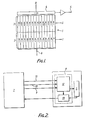
- a frame transfer image sensor 1 comprises an imaging area 2 which consists of an array of solid state photosensitive elements, a storage area 3 and a readout area 4.
- the I and S electrodes which control the movement of charge in the imaging and storage areas 2 and 3 repectively, are pulsed to cause a frame of charge from the imaging area 2 to be transfered to the storage area 3, in the direction illustrated by the arrows.
- each S electrode pulse cycle shifting a line of charge from the storage area 3 to the readout area 4.
- Readout electrodes R are controlled to transfer the charge from the readout area 4 to the output 5. If it is desired to have a short integration period, charge may be dumped in a diode drain 6 by reverse clocking.
- the image sensor 1 of Figure 1 is connected to a computer, or frame store, 7 via an interface 8.
- the interface 8 has three control line inputs 9, 10 and 11 which are arranged to carry the field control signal, the line readout control signal and the picture element control signal respectively.
- the interface 8 is such that signals applied on lines 9, 10 and 11 control the sequence and timing of signals applied to the image sensor 1 to control it, as described in greater detail with reference to Figure 3, and comprises a logic section 12 and video processing circuitry 13.
- the video processing circuitry 13 is arranged to receive the output of the image sensor 1 and convert it into a video signal which is then transmitted to the computer 7.
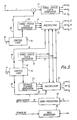
- FIG. 3 is a schematic block diagram of the interface 8 shown in Figure 2, the field control signal on control line 9 is aplied to control logic 14.
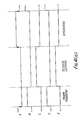
- the field control signal is shown at A on Figure 4a.
- the control logic 14 is constructed such that the falling edge of a field control pulse causes a three phase clock generator 15 to be enabled for a set number of clock pulses, the enable signal being applied on line 16 to the generator 15.
- the clock pulses are applied to two switching multiplexors 17 and 18, which are set to accept the clock pulses by signals on lines 19 and 20 respectively.
- the multiplexor 17 is set by a signal derived from the falling edge of the field control pulse, as shown at B on Figure 4a, and the multiplexor 18 is set to receive the clock pulses from generator 15 by the previous rising edge of that pulse, as shown at C.
- the multiplexors 17 and 18 pass the clock pulses to the S and I electrodes of the image sensor 1.
- the falling edge of the field control signal pulse causes the storage and image area electrodes S and I to be clocked, the number of clock pulses being sufficient to transfer a frame of charge from the image area 2 to the storage area 3.
- the frame transfer occurs over the period indicated in Figure 4a until the set number of clock pulses from clock generator 15 have been transmitted.
- the switching multiplexors 17 and 18 are switched by control signals B and C on lines 19 and 20 to cease accepting signals from the generator 15 and to receive signals on their other input lines 21 and 22 respectively.
- Reverse clocking is then initiated by enabling a reverse clocking generator 23, the duration of its output being shown at E, for a set number of pulses, to cause the image electrodes I to transfer charge contained in the elements of the image area 2 to the diode drain 6.
- This process continues until the rising edge of the field control signal is received at the control logic 14 and is arranged to stop the reverse clocking generator 23 and set the multiplexor 18 to its state in which it is able to receive clock pulses from generator 15. Integration then begins at the rising edge of the field control signal, as shown on Figure 4a.
- the line readout control signal is applied on line 10 to control logic 24 and is indicated at line F of Figure 4b.
- the control logic 24 causes a three phase clock generator 24 to be enabled for one cycle, the resulting clock pulse being applied via the multiplexer 17 to storage electrodes S1, S2, S3 as shown at lines G, H, and I of Figure 4b. This causes the transfer of a line of charge from the storage area 3 to the readout area 4.
- the line readout control signal also initiates readout of dark reference elements via line 26 to enable another three phase clock generator 27 which controls the readout electrodes R.
- the dark reference enable signal is shown at line J of Figure 4b, and the corresponding output from the readout area 4 is illustrated at line K of Figure 4b which shows the signal at the output 5 of the image sensor 1.
- the dark reference element enable signal is stopped at the rising edge of the line readout signal which also is arranged to initiate the readout of the first active picture element.
- the picture element control signal on control line 11, shown at L on Figure 4b, is applied to the clock generator 27. After each rising edge of the picture element control signal, the clock generator 27 applies a pulse to readout electrodes R and the output register of the readout area 4 is clocked to output the contents of the next picture element.
- the first rising edge of the picture element control signal causes the second active picture element to be output at 5, and subsequent rising edges cause contents of the remaining active picture elements to be read out.
- the output of the image sensor is then applied to the conventional video processing circuitry 13 to produce a video signal M. Line readout of charge contained in the storage area 3 is carried out during the integration period.
- the picture element control signal is derived from the computer store sampling signal, and is arranged to be at the same rate as it.
- the video processing circuitry 13 may be included in the interface 8 as may conventional circuitry 28 required to produce bias levels for the image sensor 1.
- the frame transfer image sensor of Figure 1 is arranged to operate normally.
- the interface 8 may also be employed with a frame transfer image sensor in full frame operation.
- Such an image sensor is illustrated in Figure 5 from which it can be seen that there is no storage area, the imaging area extending completely across the device.
- the interface 8 is used in connection with a device such as that illustrated in Figure 5, it is necessary only to set the clock generator 15 so that it runs for sufficient cycles to enable the whole of the charge stored in the imaging area to be transferred to the readout area.
- the clock generator 15 must be set to run for twice as many cycles.
- the multiplexor 18 is always set so as to receive signals from the clock generator 15, since reverse clocking is not desirable in this mode of operation.
- the signal on line 10 is only necessary to enable the dark reference elements on line 26.
- the clock generator 25 is still enabled by the falling edges of the pulses of the line readout control signal, these are not applied to the electrodes because multiplexor 17 is set to receive from the clock generator 15.
- the imaging area is covered to prevent blurring of the image. Control of the cover may be derived from the field control signal.
- the picture element control signal on line 11 operates in the same manner as described in relation to the image sensor of Figure 1.
- FIG. 6 Another form of image sensor is that known as the interline transfer type, as illustrated in Figure 6.
- the photosensitive areas 29 are interleaved with storage areas 30.
- the storage electrodes S are controlled to transfer the stored charge line by line to a readout area 31, and readout electrodes R are arranged to clock the contents of the readout area of 31 to the output.
- Readout of the stored charge normally occurs simultaneously with integration at the imaging areas 29. It is also possible to use this type of device with the interface 8 described previously.
- the control signals on the input lines 9 and 10 are arranged to produce one clock pulse from generator 15 at the end of the integration period and then sufficient clock pulses from generator 25 to transfer the charge in storage areas 30 to the readout area 31.
- TG transfer gates
- storage electrodes S storage electrodes S.
- TG transfer gates
- an interface may be devised in which the image electrodes I may be operated in the forward direction independantly of the storage electrodes S. The circuitry of the interface is then more complex but even greater flexibility is then available.
- the interface 8 may also be used with other types of image sensor, for example it may be used with an MOS imager device.
Abstract
Description
- This invention relates to imaging apparatus, and more particularly to an interface between an image sensor and a computer or computer frame store.
- There are a number of different types of image sensor available, such as, for example frame transfer image sensors, interline transfer sensors and MOS imager devices. As these operate in different manners, it has previously been necessary to build a specific interface for a particular combination of image sensor and device into which the readout of the sensor is fed. Such dedicated circuitry is known as "genlock".
- When genlock is used, line and field sync pulses are generated to initiate readout of picture information from the image sensor. The field sync pulse initiates readout of each field of picture information and the line sync pulse initiates readout of each horizontal line. After each line sync pulse, the analogue picture information from each horizontal line is sampled, and converted into a sequence of digital numbers which are stored in the computer, or frame store, memory. The rate of sampling is determined by the computer or frame store circuitry. If the image sensor is of the type in which a field of view is imaged onto a continuous surface which is scanned to produce a continuous analogue signal, this approach is acceptable. However, where the image sensor comprises an array of solid state sensors, the line of picture information is a series of discrete analogue levels which correspond to individual picture elements of the array. Unless there is exact matching between the sample rate and the picture element rate, some elements may be sampled twice or samples may be taken during the period between the readout of adjacent picture elements. This introduces inaccuracies and reduces the benefits potentially available when using precise image sensor geometry.
- The present invention seeks to provide improved imaging apparatus.
- According to the invention there is provided imaging apparatus comprising an image sensor, a device arranged to receive an output from the image sensor and an interface between them, the interface being arranged to apply a plurality of signals to the image sensor to produce the output, the sequence in which signals are applied being determined by control signals applied to the interface. Usually the device will be a computer or a frame store of a computer. Imaging apparatus in accordance with the invention is particularly advantageous since, by varying the sequence in which the plurality of signals are applied to the image sensor by the interface, a number of different types of image sensor may be employed using the same device and interface. The inventor has realised that, although considerable differences exist between different types of image sensor, certain operations or processes must be performed to all of them to obtain the readout. The first of these processes is integration, which is the period during which photogenerated charge accumulates at the optically sensitive surface of the image sensor. Also, frame initialisation is required to ready the image sensor for readout of the charge present at the photosensitive surface. Another operation which must be performed is that of line initialisation by which the image sensor is readied for readout of a new line of photogenerated charge.
- The invention is particularly advantageously employed where the image sensor comprises an array of detector elements, particularly when these are solid state elements. Where an array of discrete detector elements is employed, preferably one of the plurality of signals applied to the image sensor is arranged to read out the content of each element individually. This may be termed picture element readout. This is particularly useful since the signal controlling picture element read out may be derived from a sampling signal of the device to ensure that elements are sampled only once, thus enabling the accuracy available with such an array to be fully utilised.
- Preferably, the control signals are derived from the device arranged to receive the output, although a separate external control means could be employed. The signals required to operate an image sensor can normally be derived without difficulty from a computer for example with which the image sensor is interfaced. Preferably the plurality of signals is arranged to control the integration time, and the line readout of the image sensor.
- Advantageously, the interface comprises a plurality of lines on which respective ones of the plurality of signals are transmitted and a line arranged to receive the output of the image sensor. Lines could also be included of course for supplying power or biasing to the image sensor.
- It is preferred that the interface includes means for reverse clocking of the image sensor. This enables the integration time to be reduced by dumping some of the accumulated charge from sensor elements. This is advantageous in reducing picture blurr when fast moving objects are within the field of view of the image sensor, and can also enable adjustments to be made to suit the mean illumination level of the scene which is viewed.
- The plurality of signals may of course be of any type capable of transmitting information, but preferably they comprise pulses, rising and falling edges of which are arranged to control the production of the output of the image sensor.
- According to a feature of the invention, an interface for use in imaging apparatus in accordance with the invention comprises input means at which control signals are applied and output means at which the plurality of signals are taken.
- The interface may thus comprise circuitry which is wholly or partly controlled by the control signals to obtain the plurality of signals to be applied to the image sensor in the desired sequence.
- Some ways in which the invention may be performed are now described with reference to the accompany drawings, in which:
- Figure 1 is a schematic diagram of a frame transfer image sensor;
- Figure 2 is a schematic diagram illustrating imaging apparatus in accordance with the invention;
- Figure 3 is a schematic block diagram of the interface of Figure 2;
- Figures 4A and 4B are schematic pulse diagrams illustrating the operation of the imaging apparatus;
- Figure 5 is a schematic diagram of a frame transfer image sensor arranged to operate in a full frame mode; and
- Figure 6 illustrates schematically an interline transfer image sensor.
- With reference to Figure 1, a frame
transfer image sensor 1 comprises animaging area 2 which consists of an array of solid state photosensitive elements, astorage area 3 and a readout area 4. During the integration period, charge is allowed to accumulate in the elements of theimaging area 2. When integration is complete, the I and S electrodes, which control the movement of charge in the imaging andstorage areas imaging area 2 to be transfered to thestorage area 3, in the direction illustrated by the arrows. Then integration occurs again, during which time line initialisation also takes place, each S electrode pulse cycle shifting a line of charge from thestorage area 3 to the readout area 4. Readout electrodes R are controlled to transfer the charge from the readout area 4 to theoutput 5. If it is desired to have a short integration period, charge may be dumped in a diode drain 6 by reverse clocking. - With reference to Figure 2, the
image sensor 1 of Figure 1 is connected to a computer, or frame store, 7 via aninterface 8. Theinterface 8 has threecontrol line inputs interface 8 is such that signals applied onlines image sensor 1 to control it, as described in greater detail with reference to Figure 3, and comprises alogic section 12 andvideo processing circuitry 13. Thevideo processing circuitry 13 is arranged to receive the output of theimage sensor 1 and convert it into a video signal which is then transmitted to the computer 7. - With reference to Figure 3, which is a schematic block diagram of the
interface 8 shown in Figure 2, the field control signal oncontrol line 9 is aplied to controllogic 14. The field control signal is shown at A on Figure 4a. Thecontrol logic 14 is constructed such that the falling edge of a field control pulse causes a threephase clock generator 15 to be enabled for a set number of clock pulses, the enable signal being applied online 16 to thegenerator 15. The clock pulses are applied to twoswitching multiplexors lines multiplexor 17 is set by a signal derived from the falling edge of the field control pulse, as shown at B on Figure 4a, and themultiplexor 18 is set to receive the clock pulses fromgenerator 15 by the previous rising edge of that pulse, as shown at C. Themultiplexors image sensor 1. Thus, the falling edge of the field control signal pulse causes the storage and image area electrodes S and I to be clocked, the number of clock pulses being sufficient to transfer a frame of charge from theimage area 2 to thestorage area 3. The frame transfer occurs over the period indicated in Figure 4a until the set number of clock pulses fromclock generator 15 have been transmitted. Theswitching multiplexors lines generator 15 and to receive signals on theirother input lines - Reverse clocking is then initiated by enabling a
reverse clocking generator 23, the duration of its output being shown at E, for a set number of pulses, to cause the image electrodes I to transfer charge contained in the elements of theimage area 2 to the diode drain 6. This process continues until the rising edge of the field control signal is received at thecontrol logic 14 and is arranged to stop thereverse clocking generator 23 and set themultiplexor 18 to its state in which it is able to receive clock pulses fromgenerator 15. Integration then begins at the rising edge of the field control signal, as shown on Figure 4a. Although in this particular embodiment of the invention, it is necessary to pre-set theclock generator 15 to generate the required number of pulses to control the frame transfer and reverse clocking periods, it is of course possible to arrange the logic such that this can be controlled externally using the field control signal. - The line readout control signal is applied on
line 10 to controllogic 24 and is indicated at line F of Figure 4b. On the falling edge of the line readout control signal pulse, thecontrol logic 24 causes a threephase clock generator 24 to be enabled for one cycle, the resulting clock pulse being applied via themultiplexer 17 to storage electrodes S1, S2, S3 as shown at lines G, H, and I of Figure 4b. This causes the transfer of a line of charge from thestorage area 3 to the readout area 4. The line readout control signal also initiates readout of dark reference elements vialine 26 to enable another threephase clock generator 27 which controls the readout electrodes R. The dark reference enable signal is shown at line J of Figure 4b, and the corresponding output from the readout area 4 is illustrated at line K of Figure 4b which shows the signal at theoutput 5 of theimage sensor 1. The dark reference element enable signal is stopped at the rising edge of the line readout signal which also is arranged to initiate the readout of the first active picture element. - The picture element control signal on
control line 11, shown at L on Figure 4b, is applied to theclock generator 27. After each rising edge of the picture element control signal, theclock generator 27 applies a pulse to readout electrodes R and the output register of the readout area 4 is clocked to output the contents of the next picture element. Thus, as shown in Figure 4b, the first rising edge of the picture element control signal causes the second active picture element to be output at 5, and subsequent rising edges cause contents of the remaining active picture elements to be read out. The output of the image sensor is then applied to the conventionalvideo processing circuitry 13 to produce a video signal M. Line readout of charge contained in thestorage area 3 is carried out during the integration period. The picture element control signal is derived from the computer store sampling signal, and is arranged to be at the same rate as it. Thevideo processing circuitry 13 may be included in theinterface 8 as mayconventional circuitry 28 required to produce bias levels for theimage sensor 1. - The frame transfer image sensor of Figure 1 is arranged to operate normally. However, the
interface 8 may also be employed with a frame transfer image sensor in full frame operation. Such an image sensor is illustrated in Figure 5 from which it can be seen that there is no storage area, the imaging area extending completely across the device. When theinterface 8 is used in connection with a device such as that illustrated in Figure 5, it is necessary only to set theclock generator 15 so that it runs for sufficient cycles to enable the whole of the charge stored in the imaging area to be transferred to the readout area. Thus, where the imaging area of the full frame transfer device is comparable to that of the storage and imaging areas of the frame transfer device of Figure 1 taken together, theclock generator 15 must be set to run for twice as many cycles. Also, it is necessary to ensure that themultiplexor 18 is always set so as to receive signals from theclock generator 15, since reverse clocking is not desirable in this mode of operation. Asline 9, the signal online 10 is only necessary to enable the dark reference elements online 26. Although theclock generator 25 is still enabled by the falling edges of the pulses of the line readout control signal, these are not applied to the electrodes becausemultiplexor 17 is set to receive from theclock generator 15. During line readout, the imaging area is covered to prevent blurring of the image. Control of the cover may be derived from the field control signal. The picture element control signal online 11 operates in the same manner as described in relation to the image sensor of Figure 1. - Another form of image sensor is that known as the interline transfer type, as illustrated in Figure 6. In this device the
photosensitive areas 29 are interleaved withstorage areas 30. In operation, during integration the storage electrodes S are controlled to transfer the stored charge line by line to areadout area 31, and readout electrodes R are arranged to clock the contents of the readout area of 31 to the output. Readout of the stored charge normally occurs simultaneously with integration at theimaging areas 29. It is also possible to use this type of device with theinterface 8 described previously. The control signals on theinput lines generator 15 at the end of the integration period and then sufficient clock pulses fromgenerator 25 to transfer the charge instorage areas 30 to thereadout area 31. It may not be acceptable in some applications to have simultaneous operation of the image electrodes, which in this device are termed transfer gates (TG), and the storage electrodes S. This may be avoided by including, for example a delay line between the output of themultiplexor 17 and the storage electrodes S. Of course, an interface may be devised in which the image electrodes I may be operated in the forward direction independantly of the storage electrodes S. The circuitry of the interface is then more complex but even greater flexibility is then available. Theinterface 8 may also be used with other types of image sensor, for example it may be used with an MOS imager device.
Claims (10)
Applications Claiming Priority (2)
| Application Number | Priority Date | Filing Date | Title |
|---|---|---|---|
| GB8721977 | 1987-09-18 | ||
| GB8721977A GB2210228B (en) | 1987-09-18 | 1987-09-18 | Imaging apparatus |
Publications (2)
| Publication Number | Publication Date |
|---|---|
| EP0308075A2 true EP0308075A2 (en) | 1989-03-22 |
| EP0308075A3 EP0308075A3 (en) | 1990-05-30 |
Family
ID=10623993
Family Applications (1)
| Application Number | Title | Priority Date | Filing Date |
|---|---|---|---|
| EP88307664A Withdrawn EP0308075A3 (en) | 1987-09-18 | 1988-08-18 | Imaging apparatus |
Country Status (3)
| Country | Link |
|---|---|
| US (1) | US4896215A (en) |
| EP (1) | EP0308075A3 (en) |
| GB (1) | GB2210228B (en) |
Cited By (6)
| Publication number | Priority date | Publication date | Assignee | Title |
|---|---|---|---|---|
| WO1991010320A1 (en) * | 1989-12-28 | 1991-07-11 | Eastman Kodak Company | Electronic imaging apparatus with interchangeable pickup units |
| EP0567390A1 (en) * | 1992-04-24 | 1993-10-27 | Thomson-Csf | Digital signal processing device from optical sensors and videotransformer equipped with such a device |
| FR2695530A1 (en) * | 1992-09-10 | 1994-03-11 | Sopro Sa | Image sensor integrated into data processing system - uses video camera of which image pick=up is distant from control system, with remote sensor control unit and interface combined in extension card, and camera operated from computer system |
| EP0660617A2 (en) * | 1993-12-24 | 1995-06-28 | Canon Kabushiki Kaisha | Image pickup device |
| EP0740475A2 (en) * | 1995-04-28 | 1996-10-30 | Sony Corporation | Image pick-up apparatus |
| EP0698865A3 (en) * | 1994-07-29 | 1998-11-25 | Pitney Bowes Inc. | Charge coupled device control module |
Families Citing this family (6)
| Publication number | Priority date | Publication date | Assignee | Title |
|---|---|---|---|---|
| US5440342A (en) * | 1993-01-15 | 1995-08-08 | Eastman Kodak Company | Logic system and method for controlling any one of different charge coupled device image sensors to provide video image signals in accordance with a television standard |
| JPH0888785A (en) * | 1994-09-16 | 1996-04-02 | Toshiba Corp | Image input device |
| US5568192A (en) * | 1995-08-30 | 1996-10-22 | Intel Corporation | Method and apparatus for processing digital video camera signals |
| US7391437B2 (en) | 2002-12-18 | 2008-06-24 | Marvell International Ltd. | Image sensor interface |
| US8197231B2 (en) | 2005-07-13 | 2012-06-12 | Purity Solutions Llc | Diaphragm pump and related methods |
| US9610392B2 (en) | 2012-06-08 | 2017-04-04 | Fresenius Medical Care Holdings, Inc. | Medical fluid cassettes and related systems and methods |
Citations (2)
| Publication number | Priority date | Publication date | Assignee | Title |
|---|---|---|---|---|
| US4570184A (en) * | 1984-11-09 | 1986-02-11 | North American Philips Corporation | Optimization of vidicon bias lighting |
| EP0195270A2 (en) * | 1985-02-20 | 1986-09-24 | Matsushita Electric Industrial Co., Ltd. | Video camera apparatus |
Family Cites Families (6)
| Publication number | Priority date | Publication date | Assignee | Title |
|---|---|---|---|---|
| US4170024A (en) * | 1977-05-24 | 1979-10-02 | Rca Corporation | Television control system |
| US4740828A (en) * | 1983-12-24 | 1988-04-26 | Canon Kabushiki Kaisha | Image sensing apparatus having a low-resolution monitor, means for reducing the amount of information in an image signal, and switching means for reducing power consumption in various operating modes |
| GB2190812B (en) * | 1986-05-16 | 1990-01-17 | Gen Electric Plc | Image sensors |
| US4714963A (en) * | 1986-07-03 | 1987-12-22 | Eastman Kodak Company | Asynchronous still timing for a video camera producing movie or still images |
| US4750041A (en) * | 1986-08-21 | 1988-06-07 | Eastman Kodak Company | Apparatus for merged field operation of an image sensor in a still video camera |
| JPS6386974A (en) * | 1986-09-30 | 1988-04-18 | Nec Corp | Charge transfer image pickup element and its driving method |
-
1987
- 1987-09-18 GB GB8721977A patent/GB2210228B/en not_active Expired - Lifetime
-
1988
- 1988-08-18 EP EP88307664A patent/EP0308075A3/en not_active Withdrawn
- 1988-09-15 US US07/245,111 patent/US4896215A/en not_active Expired - Fee Related
Patent Citations (2)
| Publication number | Priority date | Publication date | Assignee | Title |
|---|---|---|---|---|
| US4570184A (en) * | 1984-11-09 | 1986-02-11 | North American Philips Corporation | Optimization of vidicon bias lighting |
| EP0195270A2 (en) * | 1985-02-20 | 1986-09-24 | Matsushita Electric Industrial Co., Ltd. | Video camera apparatus |
Cited By (12)
| Publication number | Priority date | Publication date | Assignee | Title |
|---|---|---|---|---|
| WO1991010320A1 (en) * | 1989-12-28 | 1991-07-11 | Eastman Kodak Company | Electronic imaging apparatus with interchangeable pickup units |
| EP0567390A1 (en) * | 1992-04-24 | 1993-10-27 | Thomson-Csf | Digital signal processing device from optical sensors and videotransformer equipped with such a device |
| FR2690590A1 (en) * | 1992-04-24 | 1993-10-29 | Thomson Csf | Digital signal processing device from optical sensors and video transformer equipped with at least one such device. |
| US5394186A (en) * | 1992-04-24 | 1995-02-28 | Thomson-Csf | Device for the processing of digital signals coming from optical sensors |
| FR2695530A1 (en) * | 1992-09-10 | 1994-03-11 | Sopro Sa | Image sensor integrated into data processing system - uses video camera of which image pick=up is distant from control system, with remote sensor control unit and interface combined in extension card, and camera operated from computer system |
| EP0660617A2 (en) * | 1993-12-24 | 1995-06-28 | Canon Kabushiki Kaisha | Image pickup device |
| EP0660617A3 (en) * | 1993-12-24 | 1996-04-17 | Canon Kk | Image pickup device. |
| US5712680A (en) * | 1993-12-24 | 1998-01-27 | Canon Kabushiki Kaisha | Image pickup device for obtaining both moving and still images |
| EP0698865A3 (en) * | 1994-07-29 | 1998-11-25 | Pitney Bowes Inc. | Charge coupled device control module |
| EP0740475A2 (en) * | 1995-04-28 | 1996-10-30 | Sony Corporation | Image pick-up apparatus |
| EP0740475A3 (en) * | 1995-04-28 | 1998-11-25 | Sony Corporation | Image pick-up apparatus |
| US6219096B1 (en) | 1995-04-28 | 2001-04-17 | Sony Corporation | Image signal generating and converting device |
Also Published As
| Publication number | Publication date |
|---|---|
| US4896215A (en) | 1990-01-23 |
| GB2210228A (en) | 1989-06-01 |
| GB2210228B (en) | 1991-11-13 |
| EP0308075A3 (en) | 1990-05-30 |
| GB8721977D0 (en) | 1987-10-28 |
Similar Documents
| Publication | Publication Date | Title |
|---|---|---|
| US4896215A (en) | Imaging apparatus with flexible interface for controlling different image sensor types | |
| US6608647B1 (en) | Methods and apparatus for charge coupled device image acquisition with independent integration and readout | |
| EP0748111B1 (en) | Solid image pickup unit and video camera employing same | |
| JP3817294B2 (en) | Solid-state imaging device | |
| JP3239087B2 (en) | Imaging device | |
| US6441851B1 (en) | Solid state image pickup device, signal processing method and camera therefor | |
| US5777671A (en) | Solid state imager having high frequency transfer mode | |
| US6603512B2 (en) | Imaging apparatus and control device therefor technical field | |
| US4661854A (en) | Transfer smear reduction for charge sweep device imagers | |
| JPH0442870B2 (en) | ||
| JPH06319080A (en) | Push bloom scanning type image pickup device | |
| KR20060103216A (en) | Driving controlling method for image sensing device, and imaging device | |
| WO2001063910A1 (en) | Frame shuttering scheme for increased frame rate | |
| JP3172359B2 (en) | Imaging device | |
| JP3057898B2 (en) | Solid-state imaging device and driving method thereof | |
| JP2877675B2 (en) | Solid-state imaging device | |
| JP2939997B2 (en) | Solid-state imaging device | |
| JPH079480Y2 (en) | CCD line sensor | |
| JPH0370277A (en) | Solid-state image pickup element | |
| JPH0614270A (en) | Television camera device | |
| JP2001309119A (en) | Line ccd camera | |
| JPH0965213A (en) | Image pickup device | |
| Litwiller | High-speed 6000-element digital line scan camera for machine vision | |
| JPS6436260A (en) | Picture reader | |
| JPH0787401A (en) | Solid-state image pickup device |
Legal Events
| Date | Code | Title | Description |
|---|---|---|---|
| PUAI | Public reference made under article 153(3) epc to a published international application that has entered the european phase |
Free format text: ORIGINAL CODE: 0009012 |
|
| AK | Designated contracting states |
Kind code of ref document: A2 Designated state(s): AT BE CH DE ES FR GR IT LI LU NL SE |
|
| PUAL | Search report despatched |
Free format text: ORIGINAL CODE: 0009013 |
|
| AK | Designated contracting states |
Kind code of ref document: A3 Designated state(s): AT BE CH DE ES FR GR IT LI LU NL SE |
|
| 17P | Request for examination filed |
Effective date: 19901012 |
|
| 17Q | First examination report despatched |
Effective date: 19921009 |
|
| STAA | Information on the status of an ep patent application or granted ep patent |
Free format text: STATUS: THE APPLICATION IS DEEMED TO BE WITHDRAWN |
|
| 18D | Application deemed to be withdrawn |
Effective date: 19931113 |