EP0307109A1 - Method for forming semiconductor crystal and semiconductor crystal article obtained by said method - Google Patents
Method for forming semiconductor crystal and semiconductor crystal article obtained by said method Download PDFInfo
- Publication number
- EP0307109A1 EP0307109A1 EP88307842A EP88307842A EP0307109A1 EP 0307109 A1 EP0307109 A1 EP 0307109A1 EP 88307842 A EP88307842 A EP 88307842A EP 88307842 A EP88307842 A EP 88307842A EP 0307109 A1 EP0307109 A1 EP 0307109A1
- Authority
- EP
- European Patent Office
- Prior art keywords
- ndl
- crystal
- forming
- nucleation
- semiconductor
- Prior art date
- Legal status (The legal status is an assumption and is not a legal conclusion. Google has not performed a legal analysis and makes no representation as to the accuracy of the status listed.)
- Withdrawn
Links
- 239000013078 crystal Substances 0.000 title claims abstract description 289
- 239000004065 semiconductor Substances 0.000 title claims abstract description 168
- 238000000034 method Methods 0.000 title claims description 96
- 230000006911 nucleation Effects 0.000 claims abstract description 192
- 238000010899 nucleation Methods 0.000 claims abstract description 192
- 230000008021 deposition Effects 0.000 claims abstract description 80
- 239000000758 substrate Substances 0.000 claims abstract description 70
- 229910052751 metal Inorganic materials 0.000 claims abstract description 44
- 239000002184 metal Substances 0.000 claims abstract description 44
- 239000000463 material Substances 0.000 claims description 100
- 238000000151 deposition Methods 0.000 claims description 83
- VYPSYNLAJGMNEJ-UHFFFAOYSA-N Silicium dioxide Chemical compound O=[Si]=O VYPSYNLAJGMNEJ-UHFFFAOYSA-N 0.000 claims description 57
- 239000010409 thin film Substances 0.000 claims description 57
- 229910052681 coesite Inorganic materials 0.000 claims description 27
- 229910052906 cristobalite Inorganic materials 0.000 claims description 27
- 239000000377 silicon dioxide Substances 0.000 claims description 27
- 235000012239 silicon dioxide Nutrition 0.000 claims description 27
- 229910052682 stishovite Inorganic materials 0.000 claims description 27
- 229910052905 tridymite Inorganic materials 0.000 claims description 27
- 230000015572 biosynthetic process Effects 0.000 claims description 24
- 238000005229 chemical vapour deposition Methods 0.000 claims description 6
- 229910052750 molybdenum Inorganic materials 0.000 claims description 6
- ZOKXTWBITQBERF-UHFFFAOYSA-N Molybdenum Chemical compound [Mo] ZOKXTWBITQBERF-UHFFFAOYSA-N 0.000 claims description 4
- 208000012868 Overgrowth Diseases 0.000 claims description 4
- 150000002500 ions Chemical class 0.000 claims description 4
- 239000007769 metal material Substances 0.000 claims description 4
- 239000011733 molybdenum Substances 0.000 claims description 4
- 238000000059 patterning Methods 0.000 claims description 4
- 229910052814 silicon oxide Inorganic materials 0.000 claims description 3
- 238000005468 ion implantation Methods 0.000 claims 2
- 238000012986 modification Methods 0.000 claims 1
- 230000004048 modification Effects 0.000 claims 1
- 238000009740 moulding (composite fabrication) Methods 0.000 description 71
- 229910052710 silicon Inorganic materials 0.000 description 35
- 239000010703 silicon Substances 0.000 description 31
- 239000010408 film Substances 0.000 description 24
- XUIMIQQOPSSXEZ-UHFFFAOYSA-N Silicon Chemical compound [Si] XUIMIQQOPSSXEZ-UHFFFAOYSA-N 0.000 description 19
- 239000007789 gas Substances 0.000 description 16
- 229910052782 aluminium Inorganic materials 0.000 description 9
- 229910001218 Gallium arsenide Inorganic materials 0.000 description 8
- 229910052581 Si3N4 Inorganic materials 0.000 description 8
- HQVNEWCFYHHQES-UHFFFAOYSA-N silicon nitride Chemical compound N12[Si]34N5[Si]62N3[Si]51N64 HQVNEWCFYHHQES-UHFFFAOYSA-N 0.000 description 8
- 229910052802 copper Inorganic materials 0.000 description 7
- 229910003460 diamond Inorganic materials 0.000 description 7
- 239000010432 diamond Substances 0.000 description 7
- 238000005530 etching Methods 0.000 description 7
- 229910021420 polycrystalline silicon Inorganic materials 0.000 description 5
- 239000002019 doping agent Substances 0.000 description 4
- 239000011521 glass Substances 0.000 description 4
- 239000011810 insulating material Substances 0.000 description 4
- 230000003287 optical effect Effects 0.000 description 4
- 238000005498 polishing Methods 0.000 description 4
- 230000008569 process Effects 0.000 description 4
- 229910052721 tungsten Inorganic materials 0.000 description 4
- 229910003818 SiH2Cl2 Inorganic materials 0.000 description 3
- 229910021417 amorphous silicon Inorganic materials 0.000 description 3
- 238000011161 development Methods 0.000 description 3
- 230000018109 developmental process Effects 0.000 description 3
- 238000009792 diffusion process Methods 0.000 description 3
- 238000009826 distribution Methods 0.000 description 3
- 238000004519 manufacturing process Methods 0.000 description 3
- 238000002844 melting Methods 0.000 description 3
- 230000008018 melting Effects 0.000 description 3
- 238000001020 plasma etching Methods 0.000 description 3
- 229910052594 sapphire Inorganic materials 0.000 description 3
- 239000010980 sapphire Substances 0.000 description 3
- XAGFODPZIPBFFR-UHFFFAOYSA-N aluminium Chemical compound [Al] XAGFODPZIPBFFR-UHFFFAOYSA-N 0.000 description 2
- PNEYBMLMFCGWSK-UHFFFAOYSA-N aluminium oxide Inorganic materials [O-2].[O-2].[O-2].[Al+3].[Al+3] PNEYBMLMFCGWSK-UHFFFAOYSA-N 0.000 description 2
- 238000006243 chemical reaction Methods 0.000 description 2
- 238000004581 coalescence Methods 0.000 description 2
- 230000001276 controlling effect Effects 0.000 description 2
- 230000000875 corresponding effect Effects 0.000 description 2
- 230000007547 defect Effects 0.000 description 2
- 230000000694 effects Effects 0.000 description 2
- 229910052732 germanium Inorganic materials 0.000 description 2
- 230000010354 integration Effects 0.000 description 2
- 238000001459 lithography Methods 0.000 description 2
- 229910021645 metal ion Inorganic materials 0.000 description 2
- 150000002739 metals Chemical class 0.000 description 2
- 239000000203 mixture Substances 0.000 description 2
- 238000001451 molecular beam epitaxy Methods 0.000 description 2
- 239000012495 reaction gas Substances 0.000 description 2
- 238000011160 research Methods 0.000 description 2
- 229920006395 saturated elastomer Polymers 0.000 description 2
- 239000007790 solid phase Substances 0.000 description 2
- 238000007711 solidification Methods 0.000 description 2
- 230000008023 solidification Effects 0.000 description 2
- 229910016570 AlCu Inorganic materials 0.000 description 1
- ZOXJGFHDIHLPTG-UHFFFAOYSA-N Boron Chemical compound [B] ZOXJGFHDIHLPTG-UHFFFAOYSA-N 0.000 description 1
- 239000004215 Carbon black (E152) Substances 0.000 description 1
- 244000126211 Hericium coralloides Species 0.000 description 1
- 229910003910 SiCl4 Inorganic materials 0.000 description 1
- 229910004014 SiF4 Inorganic materials 0.000 description 1
- 229910003822 SiHCl3 Inorganic materials 0.000 description 1
- BLRPTPMANUNPDV-UHFFFAOYSA-N Silane Chemical compound [SiH4] BLRPTPMANUNPDV-UHFFFAOYSA-N 0.000 description 1
- 238000010521 absorption reaction Methods 0.000 description 1
- 229910045601 alloy Inorganic materials 0.000 description 1
- 239000000956 alloy Substances 0.000 description 1
- 229910052796 boron Inorganic materials 0.000 description 1
- 239000013590 bulk material Substances 0.000 description 1
- 239000012159 carrier gas Substances 0.000 description 1
- 239000000919 ceramic Substances 0.000 description 1
- 238000002109 crystal growth method Methods 0.000 description 1
- 229910021419 crystalline silicon Inorganic materials 0.000 description 1
- 230000001419 dependent effect Effects 0.000 description 1
- 238000005137 deposition process Methods 0.000 description 1
- 238000010894 electron beam technology Methods 0.000 description 1
- 230000005284 excitation Effects 0.000 description 1
- 230000008570 general process Effects 0.000 description 1
- 230000020169 heat generation Effects 0.000 description 1
- 229930195733 hydrocarbon Natural products 0.000 description 1
- 150000002430 hydrocarbons Chemical class 0.000 description 1
- 230000000977 initiatory effect Effects 0.000 description 1
- 238000002347 injection Methods 0.000 description 1
- 239000007924 injection Substances 0.000 description 1
- 239000012212 insulator Substances 0.000 description 1
- 230000003993 interaction Effects 0.000 description 1
- 238000010030 laminating Methods 0.000 description 1
- 239000004973 liquid crystal related substance Substances 0.000 description 1
- 239000007791 liquid phase Substances 0.000 description 1
- 239000011159 matrix material Substances 0.000 description 1
- 238000005259 measurement Methods 0.000 description 1
- 239000005300 metallic glass Substances 0.000 description 1
- 229910021421 monocrystalline silicon Inorganic materials 0.000 description 1
- 125000002524 organometallic group Chemical group 0.000 description 1
- 239000012071 phase Substances 0.000 description 1
- 238000002360 preparation method Methods 0.000 description 1
- LIVNPJMFVYWSIS-UHFFFAOYSA-N silicon monoxide Chemical compound [Si-]#[O+] LIVNPJMFVYWSIS-UHFFFAOYSA-N 0.000 description 1
- FDNAPBUWERUEDA-UHFFFAOYSA-N silicon tetrachloride Chemical compound Cl[Si](Cl)(Cl)Cl FDNAPBUWERUEDA-UHFFFAOYSA-N 0.000 description 1
- ABTOQLMXBSRXSM-UHFFFAOYSA-N silicon tetrafluoride Chemical compound F[Si](F)(F)F ABTOQLMXBSRXSM-UHFFFAOYSA-N 0.000 description 1
- 239000000243 solution Substances 0.000 description 1
- 238000004544 sputter deposition Methods 0.000 description 1
- 238000002230 thermal chemical vapour deposition Methods 0.000 description 1
- WFKWXMTUELFFGS-UHFFFAOYSA-N tungsten Chemical compound [W] WFKWXMTUELFFGS-UHFFFAOYSA-N 0.000 description 1
- 239000010937 tungsten Substances 0.000 description 1
- 238000007740 vapor deposition Methods 0.000 description 1
- 238000001947 vapour-phase growth Methods 0.000 description 1
Images


Classifications
-
- H—ELECTRICITY
- H01—ELECTRIC ELEMENTS
- H01L—SEMICONDUCTOR DEVICES NOT COVERED BY CLASS H10
- H01L31/00—Semiconductor devices sensitive to infrared radiation, light, electromagnetic radiation of shorter wavelength or corpuscular radiation and specially adapted either for the conversion of the energy of such radiation into electrical energy or for the control of electrical energy by such radiation; Processes or apparatus specially adapted for the manufacture or treatment thereof or of parts thereof; Details thereof
- H01L31/18—Processes or apparatus specially adapted for the manufacture or treatment of these devices or of parts thereof
- H01L31/1804—Processes or apparatus specially adapted for the manufacture or treatment of these devices or of parts thereof comprising only elements of Group IV of the Periodic System
-
- C—CHEMISTRY; METALLURGY
- C30—CRYSTAL GROWTH
- C30B—SINGLE-CRYSTAL GROWTH; UNIDIRECTIONAL SOLIDIFICATION OF EUTECTIC MATERIAL OR UNIDIRECTIONAL DEMIXING OF EUTECTOID MATERIAL; REFINING BY ZONE-MELTING OF MATERIAL; PRODUCTION OF A HOMOGENEOUS POLYCRYSTALLINE MATERIAL WITH DEFINED STRUCTURE; SINGLE CRYSTALS OR HOMOGENEOUS POLYCRYSTALLINE MATERIAL WITH DEFINED STRUCTURE; AFTER-TREATMENT OF SINGLE CRYSTALS OR A HOMOGENEOUS POLYCRYSTALLINE MATERIAL WITH DEFINED STRUCTURE; APPARATUS THEREFOR
- C30B25/00—Single-crystal growth by chemical reaction of reactive gases, e.g. chemical vapour-deposition growth
- C30B25/02—Epitaxial-layer growth
- C30B25/18—Epitaxial-layer growth characterised by the substrate
-
- H—ELECTRICITY
- H01—ELECTRIC ELEMENTS
- H01L—SEMICONDUCTOR DEVICES NOT COVERED BY CLASS H10
- H01L21/00—Processes or apparatus adapted for the manufacture or treatment of semiconductor or solid state devices or of parts thereof
- H01L21/02—Manufacture or treatment of semiconductor devices or of parts thereof
- H01L21/02104—Forming layers
- H01L21/02365—Forming inorganic semiconducting materials on a substrate
- H01L21/02367—Substrates
- H01L21/0237—Materials
- H01L21/02422—Non-crystalline insulating materials, e.g. glass, polymers
-
- H—ELECTRICITY
- H01—ELECTRIC ELEMENTS
- H01L—SEMICONDUCTOR DEVICES NOT COVERED BY CLASS H10
- H01L21/00—Processes or apparatus adapted for the manufacture or treatment of semiconductor or solid state devices or of parts thereof
- H01L21/02—Manufacture or treatment of semiconductor devices or of parts thereof
- H01L21/02104—Forming layers
- H01L21/02365—Forming inorganic semiconducting materials on a substrate
- H01L21/02436—Intermediate layers between substrates and deposited layers
- H01L21/02439—Materials
- H01L21/02441—Group 14 semiconducting materials
- H01L21/0245—Silicon, silicon germanium, germanium
-
- H—ELECTRICITY
- H01—ELECTRIC ELEMENTS
- H01L—SEMICONDUCTOR DEVICES NOT COVERED BY CLASS H10
- H01L21/00—Processes or apparatus adapted for the manufacture or treatment of semiconductor or solid state devices or of parts thereof
- H01L21/02—Manufacture or treatment of semiconductor devices or of parts thereof
- H01L21/02104—Forming layers
- H01L21/02365—Forming inorganic semiconducting materials on a substrate
- H01L21/02436—Intermediate layers between substrates and deposited layers
- H01L21/02439—Materials
- H01L21/02455—Group 13/15 materials
- H01L21/02463—Arsenides
-
- H—ELECTRICITY
- H01—ELECTRIC ELEMENTS
- H01L—SEMICONDUCTOR DEVICES NOT COVERED BY CLASS H10
- H01L21/00—Processes or apparatus adapted for the manufacture or treatment of semiconductor or solid state devices or of parts thereof
- H01L21/02—Manufacture or treatment of semiconductor devices or of parts thereof
- H01L21/02104—Forming layers
- H01L21/02365—Forming inorganic semiconducting materials on a substrate
- H01L21/02518—Deposited layers
- H01L21/02521—Materials
- H01L21/02524—Group 14 semiconducting materials
- H01L21/02532—Silicon, silicon germanium, germanium
-
- H—ELECTRICITY
- H01—ELECTRIC ELEMENTS
- H01L—SEMICONDUCTOR DEVICES NOT COVERED BY CLASS H10
- H01L21/00—Processes or apparatus adapted for the manufacture or treatment of semiconductor or solid state devices or of parts thereof
- H01L21/02—Manufacture or treatment of semiconductor devices or of parts thereof
- H01L21/02104—Forming layers
- H01L21/02365—Forming inorganic semiconducting materials on a substrate
- H01L21/02518—Deposited layers
- H01L21/0257—Doping during depositing
- H01L21/02573—Conductivity type
- H01L21/02576—N-type
-
- H—ELECTRICITY
- H01—ELECTRIC ELEMENTS
- H01L—SEMICONDUCTOR DEVICES NOT COVERED BY CLASS H10
- H01L21/00—Processes or apparatus adapted for the manufacture or treatment of semiconductor or solid state devices or of parts thereof
- H01L21/02—Manufacture or treatment of semiconductor devices or of parts thereof
- H01L21/02104—Forming layers
- H01L21/02365—Forming inorganic semiconducting materials on a substrate
- H01L21/02518—Deposited layers
- H01L21/0257—Doping during depositing
- H01L21/02573—Conductivity type
- H01L21/02579—P-type
-
- H—ELECTRICITY
- H01—ELECTRIC ELEMENTS
- H01L—SEMICONDUCTOR DEVICES NOT COVERED BY CLASS H10
- H01L21/00—Processes or apparatus adapted for the manufacture or treatment of semiconductor or solid state devices or of parts thereof
- H01L21/02—Manufacture or treatment of semiconductor devices or of parts thereof
- H01L21/02104—Forming layers
- H01L21/02365—Forming inorganic semiconducting materials on a substrate
- H01L21/02612—Formation types
- H01L21/02617—Deposition types
- H01L21/0262—Reduction or decomposition of gaseous compounds, e.g. CVD
-
- H—ELECTRICITY
- H01—ELECTRIC ELEMENTS
- H01L—SEMICONDUCTOR DEVICES NOT COVERED BY CLASS H10
- H01L21/00—Processes or apparatus adapted for the manufacture or treatment of semiconductor or solid state devices or of parts thereof
- H01L21/02—Manufacture or treatment of semiconductor devices or of parts thereof
- H01L21/02104—Forming layers
- H01L21/02365—Forming inorganic semiconducting materials on a substrate
- H01L21/02612—Formation types
- H01L21/02617—Deposition types
- H01L21/02636—Selective deposition, e.g. simultaneous growth of mono- and non-monocrystalline semiconductor materials
- H01L21/02639—Preparation of substrate for selective deposition
-
- H—ELECTRICITY
- H01—ELECTRIC ELEMENTS
- H01L—SEMICONDUCTOR DEVICES NOT COVERED BY CLASS H10
- H01L21/00—Processes or apparatus adapted for the manufacture or treatment of semiconductor or solid state devices or of parts thereof
- H01L21/02—Manufacture or treatment of semiconductor devices or of parts thereof
- H01L21/02104—Forming layers
- H01L21/02365—Forming inorganic semiconducting materials on a substrate
- H01L21/02612—Formation types
- H01L21/02617—Deposition types
- H01L21/02636—Selective deposition, e.g. simultaneous growth of mono- and non-monocrystalline semiconductor materials
- H01L21/02647—Lateral overgrowth
-
- H—ELECTRICITY
- H01—ELECTRIC ELEMENTS
- H01L—SEMICONDUCTOR DEVICES NOT COVERED BY CLASS H10
- H01L31/00—Semiconductor devices sensitive to infrared radiation, light, electromagnetic radiation of shorter wavelength or corpuscular radiation and specially adapted either for the conversion of the energy of such radiation into electrical energy or for the control of electrical energy by such radiation; Processes or apparatus specially adapted for the manufacture or treatment thereof or of parts thereof; Details thereof
- H01L31/0248—Semiconductor devices sensitive to infrared radiation, light, electromagnetic radiation of shorter wavelength or corpuscular radiation and specially adapted either for the conversion of the energy of such radiation into electrical energy or for the control of electrical energy by such radiation; Processes or apparatus specially adapted for the manufacture or treatment thereof or of parts thereof; Details thereof characterised by their semiconductor bodies
- H01L31/0352—Semiconductor devices sensitive to infrared radiation, light, electromagnetic radiation of shorter wavelength or corpuscular radiation and specially adapted either for the conversion of the energy of such radiation into electrical energy or for the control of electrical energy by such radiation; Processes or apparatus specially adapted for the manufacture or treatment thereof or of parts thereof; Details thereof characterised by their semiconductor bodies characterised by their shape or by the shapes, relative sizes or disposition of the semiconductor regions
- H01L31/035272—Semiconductor devices sensitive to infrared radiation, light, electromagnetic radiation of shorter wavelength or corpuscular radiation and specially adapted either for the conversion of the energy of such radiation into electrical energy or for the control of electrical energy by such radiation; Processes or apparatus specially adapted for the manufacture or treatment thereof or of parts thereof; Details thereof characterised by their semiconductor bodies characterised by their shape or by the shapes, relative sizes or disposition of the semiconductor regions characterised by at least one potential jump barrier or surface barrier
- H01L31/03529—Shape of the potential jump barrier or surface barrier
-
- H—ELECTRICITY
- H01—ELECTRIC ELEMENTS
- H01L—SEMICONDUCTOR DEVICES NOT COVERED BY CLASS H10
- H01L31/00—Semiconductor devices sensitive to infrared radiation, light, electromagnetic radiation of shorter wavelength or corpuscular radiation and specially adapted either for the conversion of the energy of such radiation into electrical energy or for the control of electrical energy by such radiation; Processes or apparatus specially adapted for the manufacture or treatment thereof or of parts thereof; Details thereof
- H01L31/04—Semiconductor devices sensitive to infrared radiation, light, electromagnetic radiation of shorter wavelength or corpuscular radiation and specially adapted either for the conversion of the energy of such radiation into electrical energy or for the control of electrical energy by such radiation; Processes or apparatus specially adapted for the manufacture or treatment thereof or of parts thereof; Details thereof adapted as photovoltaic [PV] conversion devices
- H01L31/042—PV modules or arrays of single PV cells
- H01L31/0475—PV cell arrays made by cells in a planar, e.g. repetitive, configuration on a single semiconductor substrate; PV cell microarrays
-
- Y—GENERAL TAGGING OF NEW TECHNOLOGICAL DEVELOPMENTS; GENERAL TAGGING OF CROSS-SECTIONAL TECHNOLOGIES SPANNING OVER SEVERAL SECTIONS OF THE IPC; TECHNICAL SUBJECTS COVERED BY FORMER USPC CROSS-REFERENCE ART COLLECTIONS [XRACs] AND DIGESTS
- Y02—TECHNOLOGIES OR APPLICATIONS FOR MITIGATION OR ADAPTATION AGAINST CLIMATE CHANGE
- Y02E—REDUCTION OF GREENHOUSE GAS [GHG] EMISSIONS, RELATED TO ENERGY GENERATION, TRANSMISSION OR DISTRIBUTION
- Y02E10/00—Energy generation through renewable energy sources
- Y02E10/50—Photovoltaic [PV] energy
- Y02E10/547—Monocrystalline silicon PV cells
-
- Y—GENERAL TAGGING OF NEW TECHNOLOGICAL DEVELOPMENTS; GENERAL TAGGING OF CROSS-SECTIONAL TECHNOLOGIES SPANNING OVER SEVERAL SECTIONS OF THE IPC; TECHNICAL SUBJECTS COVERED BY FORMER USPC CROSS-REFERENCE ART COLLECTIONS [XRACs] AND DIGESTS
- Y02—TECHNOLOGIES OR APPLICATIONS FOR MITIGATION OR ADAPTATION AGAINST CLIMATE CHANGE
- Y02P—CLIMATE CHANGE MITIGATION TECHNOLOGIES IN THE PRODUCTION OR PROCESSING OF GOODS
- Y02P70/00—Climate change mitigation technologies in the production process for final industrial or consumer products
- Y02P70/50—Manufacturing or production processes characterised by the final manufactured product
-
- Y—GENERAL TAGGING OF NEW TECHNOLOGICAL DEVELOPMENTS; GENERAL TAGGING OF CROSS-SECTIONAL TECHNOLOGIES SPANNING OVER SEVERAL SECTIONS OF THE IPC; TECHNICAL SUBJECTS COVERED BY FORMER USPC CROSS-REFERENCE ART COLLECTIONS [XRACs] AND DIGESTS
- Y10—TECHNICAL SUBJECTS COVERED BY FORMER USPC
- Y10S—TECHNICAL SUBJECTS COVERED BY FORMER USPC CROSS-REFERENCE ART COLLECTIONS [XRACs] AND DIGESTS
- Y10S428/00—Stock material or miscellaneous articles
- Y10S428/901—Printed circuit
-
- Y—GENERAL TAGGING OF NEW TECHNOLOGICAL DEVELOPMENTS; GENERAL TAGGING OF CROSS-SECTIONAL TECHNOLOGIES SPANNING OVER SEVERAL SECTIONS OF THE IPC; TECHNICAL SUBJECTS COVERED BY FORMER USPC CROSS-REFERENCE ART COLLECTIONS [XRACs] AND DIGESTS
- Y10—TECHNICAL SUBJECTS COVERED BY FORMER USPC
- Y10T—TECHNICAL SUBJECTS COVERED BY FORMER US CLASSIFICATION
- Y10T428/00—Stock material or miscellaneous articles
- Y10T428/24—Structurally defined web or sheet [e.g., overall dimension, etc.]
- Y10T428/24802—Discontinuous or differential coating, impregnation or bond [e.g., artwork, printing, retouched photograph, etc.]
- Y10T428/24917—Discontinuous or differential coating, impregnation or bond [e.g., artwork, printing, retouched photograph, etc.] including metal layer
-
- Y—GENERAL TAGGING OF NEW TECHNOLOGICAL DEVELOPMENTS; GENERAL TAGGING OF CROSS-SECTIONAL TECHNOLOGIES SPANNING OVER SEVERAL SECTIONS OF THE IPC; TECHNICAL SUBJECTS COVERED BY FORMER USPC CROSS-REFERENCE ART COLLECTIONS [XRACs] AND DIGESTS
- Y10—TECHNICAL SUBJECTS COVERED BY FORMER USPC
- Y10T—TECHNICAL SUBJECTS COVERED BY FORMER US CLASSIFICATION
- Y10T428/00—Stock material or miscellaneous articles
- Y10T428/31504—Composite [nonstructural laminate]
- Y10T428/31678—Of metal
Definitions
- This invention relates to a method for forming a semiconductor crystal and a semiconductor crystal article obtained by said method, particularly to a method for forming a semiconductor single crystal or a semiconductor polycrystal controlled in grain size prepared by utilizing the difference in nucleation density of the deposited materials according to the kinds of the deposited surface materials, and a crystal article obtained by said method.
- the present invention is applicable for formation of a semiconductor crystal such as a semiconductor single cyrstal or a semiconductor polycrystal to be used for electronic devices, optical devices, magnetic devices, piezoelectric devices or surface acoustic devices, etc., such as semiconductor integrated circuits, optical integrated circuits, magnetic circuits, etc.
- single crystal thin films to be used for semiconductor electronic devices or optical devices have been formed by epitaxial growth on a single crystal substrate.
- epitaxial growth of Si, Ge, GaAs, etc. can be done from liquid phase, gas phase or solid phase on Si single crystal substrate (silicon wafer), and it has been also known that epitaxial growth of a single crystal such as GaAs, GaAlAs, etc., occurs on a GaAs single crystal substrate.
- semiconductor devices and integrated circuits, electroluminescent devices such as semiconductor lasers or LED have been prepared.
- the method for forming a single crystal thin film of the prior art by epitaxial growth may be understood to be dependent greatly on its substrate material.
- Mathews et al have examined about combinations of the substrate material with epitaxial growth layer (EPITAXIAL GROWTH, Academic Press, New York, 1975, ed. by J.W. Mathews).
- the size of the substrate is presently about 6 inches for Si wafer, and enlargement of GaAs, sapphire substrate is further retarded.
- the single crystal substrate is high in production cost, the cost per chip becomes higher.
- the crystal structure of the deposited film becomes amorphous or polycrystalline.
- the amorphous film refers to a state in which near distance order to the extent of the closest atoms is preserved, but no longer distance order exists, while the polycrystalline film refers to single crystal grains having no specific crystal direction gathered as separated at the grain boundaries.
- the deposition temperature is about 600°C or lower, it becomes an amorphous silicon, while it becomes a polycrystalline silicon with grain sizes distributed between some hundred to some thousand ⁇ at a temperature higher than said temperature.
- the grain sizes and their distribution of polycrystalline silicon will be varied greatly depending on the formation method.
- the method for forming a polycrystalline thin film with great grain sizes by melting and solidification had the problems that an enormous time is required due to scanning of amorphous or single crystal thin film with energy beam for every wafer to be poor in bulk productivity, and also that it is not suited for enlargement of area.
- Diamond thin film which is particularly broad in bandgap as 5.5 eV as the semiconductor, can be actuated at higher temperature (about 500°C or less) as compared with Si, Ge, GaAs, etc., which are semiconductor materials of the prior art. Also, the carrier mobility of both electrons and positive holes surpass that of Si (1800 cm2/V ⁇ sec for electrons, 1600 cm2/V ⁇ sec for positive holes), and thermal conductivity is also extremely high. For this reason, it has been expected to be promising for application in semiconductor devices of the great consumption power type with great heat generation quantity.
- diamond nuclei are generated by utilizing excitation with microwave, using a hydrocarbon type gas such as CH4, etc., and by irradiation with hot filament or electron beam, but the nucleation density is generally low, whereby a continuous thin film can be obtained with difficulty. Even if a continuous thin film may be formed, it has a polycrystalline structure with great grain size distribution and can be difficultly applied for semiconductor device.
- a main object of the present invention is to provide a method for forming a semiconductor crystal which has overcome the problems of the prior art as described above and a crystal article obtained by said method.
- Another object of the present invention is to provide a method for forming a semiconductor crystal of good quality such as single crystal containing no grain boundary or a polycrystal controlled in grain boundary, etc., without restriction with respect to the base materials, for example, without restriction with respect to materials, constitutions, sizes, etc., of the substrate, and a crystal article having the crystal obtained by said method.
- Still another object of the present invention is to provide a method for forming the above semiconductor crystal with good efficiency according to simple steps without use of a special device.
- Still another object of the present invention is to provide a semiconductor crystal article having a semiconductor single crystal which is grown singly on a nucleation surface (S NDL ), which nucleation surface (S NDL ) is formed on a crystal forming surface with a metal having sufficiently greater nucleation density (ND) than the material forming said crystal forming surface and has a sufficiently small area to the extent that only a single nucleus can be grown.
- S NDL nucleation surface
- ND nucleation density
- Still another object of the present invention is to provide a method for forming a semiconductor crystal by utilizing the difference in nucleation density of the crystal forming materials according to the kinds of the materials forming the crystal forming surface, which comprises forming on said crystal forming surface a nucleation surface (S NDL ) with a metal having sufficiently greater nucleation density than the material forming said crystal forming surface having a sufficiently small area so that only a single nucleus may grow thereon, forming only a single nucleus on said nucleation surface (S NDL ), and growing a single crystal from said single nucleus, thereby forming a semiconductor crystal.
- S NDL nucleation surface
- Still another object of the present invention is to provide a method for forming a semiconductor crystal, which comprises applying a crystal forming treatment on a substrate having a free surface on which a nonnucleation surface (S NDS ) with a small nucleation density and a nucleation surface (S NDL ) with a metal having a sufficiently small area for crystal growth only from a single nucleus and having a greater nucleation density (ND L ) than the nucleation density (ND S ) of said nonnucleation surface (S NDS ) are arranged adjacent to each other, thereby growing a semiconductor single crystal from said single nucleus.
- S NDS nonnucleation surface
- S NDL nucleation surface
- Still another object of the present invention is to provide a method for forming a semiconductor crystal, which comprises forming, on a substrate having a small nonnucleation surface (S NDS ) with samll nucleation density at a small area for a crystal growth from only a single nucleus at a desired position of said nonnucleation surface (S NDS ), a nucleation surface (S NDL ) having greater nucleation density (ND L ) than the nucleation density (ND S ) of said nonnucleation surface (S NDS ) by addtion of a metal (M L ) for forming said nucleation surface (S NDL ) which is different from the material (M S ) forming said nonnucleation surface (S NDS ), and then applying a crystal forming treatment on said substrate to form a single crystal nucleus on said nucleation surface (S NDL ), thereby growing a semiconductor single crystal from said single nucleus.
- S NDS small nonnucleation surface
- Still another object of the present invention is to provide a method for forming a semiconductor crystal, which comprises applying a crystal forming treatment on a substrate having two kinds of surface with a sufficiently great nucleation density difference ( ⁇ ND), of which the surface (S NDL ) with smaller nucleation density has a sufficiently small area for growth of a semiconductor single crystal from only a single nucleus to form a stable single nucleus on said surface (S NDL ), thereby growing a semiconductor single crystal from said single nucleus.
- ⁇ ND nucleation density difference
- Still another object of the present invention is to provide a semiconductor crystal article, comprising a substrate having a nonnucleation surface (S NDS ) with small nucleation density and a nucleation surface (S NDL ) with a metal, arranged adjacent to said nonnucleation surface (S NDS ), having a sufficiently small area for crystal growth from only a single nucleus and having greater nucleation density (ND L ) than the nucleation density (ND S ) of said nonnucleation surface (S NDS ), and a single crystal which grows from said single nucleus and covers sufficiently over said nucleation surface (S NDL ).
- the nucleus with the size exceeding rc is called stable nucleus, and unless otherwise particularly noted, “nucleus” in the following basic description of the present invention refers to this "stable nucleus". Also, among “stable nucleus”, those with small r are called “initial nucleus”.
- Fig. 1 shows the manner in which G is changed. In the same Figure, the radius of curvature of the stable nucleus when G is at the maximum value is rc.
- nuclei grow to become shaped in islands, and further grow whereby contact mutually between islands progresses until sometimes coalescence occurs and via a network structure, it becomes finally a continuous film to cover completely over the substrate surface. Following such a process, a thin film is deposited on the substrate.
- the density of nucleus formed per unit area of the substrate surface, the size of nucleus and the nucleation speed are determined depending on the state of the system of deposition, and particularly the interaction between the flying atoms and the substrate surface material is an important factor.
- a specific crystal direction grows in parallel to the substrate due to anisotropy relative to the crystal surface of the interface energy at the interface between the deposited material and the substrate, and when the substrate is amorphous, the crystal direction within the substrate plane is not constant.
- grain boundaries are formed by collision mutually between nuclei or islands, and particularly in the case of collision mutually between islands with some sizes or greater, grain boundaries are formed as such rather than occurrence of coalescence. Since the grain boundaries formed are difficulty movable in the solid phase, the grain sizes are determined at that point.
- the selective deposition method is a method in which a thin film is formed selectively on the substrate by utilizing the differences between the materials in factors influencing nucleus formation in the thin film forming process such as surface energy, attachment coefficient, release coefficinet, surface diffusion speed, etc.
- Figs. 2A and 2B are illustrations of the selective deposition method.
- a thin film 2 comprising a material different in the above factors from the substrate 1 is formed at a desired portion.
- a thin film 3 grows only on the thin film 2, whereby it is possible to give rise to a phenomenon that no growth occurs on the substrate 1.
- the thin film 3 formed self-matchingly can be grown, whereby it becomes possible to omit the lithographic step by use of a resist as practiced in the prior art.
- SiO2 may be used as the substrate 1, Si, GaAs, silicon nitride as the thin film 2 and Si, W, GaAs, InP, etc., as the thin film 3 to be deposited.
- Fig. 3 is a graph showing the change with lapse of time of nucleation density on the deposited surface of SiO2 and the deposited surface of silicon nitride.
- the nucleation density on SiO2 is saturated at 103 cm ⁇ 2 or less, and the value is not substantially changed even after 20 minutes.
- SiCl4 gas is diluted with H2 and deposited according to the CVD method under the conditions of a pressure of 170 Torr and a temperature of 1000°C. Otherwise, the same action can be obtained by use of SiH4, SiH2Cl2, SiHCl3, SiF4, etc., as the reaction gas, and controlling the pressure, temperature, etc. Also, the vacuum vapor deposition can be employed.
- nucleation on SiO2 poses substantially no problem, but by addition of HCl gas into the reaction gas, nucleation on SiO2 can be further suppressed to make deposition of Si on SiO2 perfectly zero.
- Such a phenomenon depends greatly on the difference in absorption coefficient, release coefficient, surface diffusion coefficient, etc., relative to Si of the material surfaces of SiO2 and silicon nitride, but the fact that SiO2 itself is etched by the reaction of SiO2 with Si atom itself to form silicon monooxide with higher vapor pressure, while no such etching phenomenon occurs on silicon nitride may be also considered to be a cause to effect selective deposition (T. Yonehara, S. Yoshioka, S. Miyazawa, Journal of Applied Physics 53, 6839, 1982).
- SiO2 and silicon nitride as the materials of the deposition surface and silicon as the material to be deposited, sufficiently great nucleation density difference as shown in the same graph can be obtained.
- SiO2 is desirable as the material for the nonnucleation surface, this is not limitative and sufficiently practial nucleation density difference can be obtained even by use of SiO x (0 ⁇ x ⁇ 2).
- nucleation density may be sufficiently 103-fold or more in density of nuclei as shown by the same graph, and sufficient selective formation of deposited film can be done with the materials as examplified below.
- ions of Al or Cu may be injected locally into the SiO2 surface to form a region having excessive Al or Cu.
- the present invention utilizes selective deposition based on such nucleation density difference ( ⁇ ND) and, by forming sufficiently finely so that a single nucleus may grow on the necleation surface of a different kind of material having sufficiently greater nucleation density than the material of the nonnucleation surface, a single crystal of semiconductor can be grown selectively only at the site where such fine different kind of material exists.
- ⁇ ND nucleation density difference
- the material with lower nucleation density (for example, SiO2) is not required to be a bulk material, but it may be formed only on the surface of any desired material, substrate, etc., to form the above deposited surface.
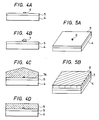
- Figs. 4A to 4D are illustrations of the formation steps showing a first embodiment of the method for forming semiconductor crystal according to the present invention
- Figs. 5A and 5B are perspective views of the substrates in Figs. 4A and 4D.
- a thin film 5 [deposition surface (S NDS )] with small nucleation density which enables selective deposition is formed and a metallic material different from the material forming the thin film 5 with greater nucleation density is deposited thinly, followed by patterning according to lithography, etc., to form sufficiently finely nucleation surface 6 (S NDL ) (or called "Seed”) comprising a different kind of material.
- S NDL deposition surface
- the size, the crystal structure and the composition of the support 4 may be any desired ones, and a support having a functional device formed thereon prepared according to conventional semiconductor technique may be employed.
- the nucleation surface (S NDL ) 6 comprising a different kind of material is also inclusive of modified regions having excessive metals formed by metal ion injection into the thin film 5 as described above.
- the nucleation surface (S NDL ) 6 is required to be formed sufficiently finely so that only a single nucleus may be formed thereon.
- the nucleus grows while maintaining a single crystal structure to become a semiconductor single crystal grain 7 in shape of an island as shown in Fig. 4B. For forming an island-shaped single crystal grain 7, it is desirable to determine the conditions so that no nucleation may occur at all on the thin film 5, as already mentioned.
- the island-shaped semiconductor single crystal grain 7 further grows while maintaining the single crystal structure with the nucleation surface (S NDL ) 6 as the center (lateral overgrowth), whereby it can cover over the whole thin film 5 as shown in Fig. 4C (single crystal 7A).
- the semiconductor single crystal 7A is flattened by etching or polishing, and a single crystal layer 8 capable of forming a desired device can be formed on the thin film 5 as shown in Fig. 4D and Fig. 5B.
- any desired material can be used for the support 4 any desired material can be used for the support 4 which is the supporting member. Further, in such a case, even when the support 4 may be one having a functional device, etc., formed thereon according to conventional semiconductor technique, the single crystal layer 8 can be easily formed thereon.
- the nonnucleation surface (S NDS ) is formed of thin film 5, but a support comprising a material with small nucleation density (ND) enabling selective nucleation may be used as such and nucleation surfaces (S NDL ) may be provided at any desired positions to form single crystal layers similarly thereon.
- ND nucleation density
- Figs. 6A - 6D are illustrations of the steps for forming semiconductor crystal showing a second embodiment of the present invention.
- the nucleation surface (S NDL ) comprising a metal with great nucleation density (ND) can be formed sufficiently finely to form a semiconductor single crystal 7A similarly as in the first embodiment.
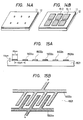
- Figs. 7A - 7D are illustrations of the formation steps showing a third embodiment of the method for forming semiconductor crystal according to the present invention
- Figs. 8A and 8B are perspective views of the substrates in Figs. 7A and 7D.
- nucleation surfaces (S NDL ) 12-1, 12-2 of a metal different from the support 11 enabling the above selective nucleation are arranged sufficiently finely.
- the distance l is set equal to the size of the single crystal region required for formation of semiconductor device or group of devices or greater.
- the nucleation surfaces (S NDL ) 12-1, 12-2 are required to be formed to a sufficiently fine size (area) to the extent that only a single nucleus may be formed.
- the size of the nucleation surfaces (S NDL ) 12-1, 12-2, which may be different depending on the kind of the material, may be several microns or less.
- the nucleus grows while maintaining the single crystal structure, and become island-shaped semiconductor single crystal grains 13-1, 13-2 as shown in Fig. 7B.
- the crystal direction in the normal line direction of the support 11 of the island-shaped semiconductor single crystal grains 13-1, 13-2 is determined so as to make the interface energy of the material of the support 11 and the material formig nucleus minimum.
- For surface or interface energy has anisotropy depending on the crystal face.
- the crystal direction within the support plane in amorphous support is not determined.
- the island-shaped semiconductor single crystal grains 13-1, 13-2 further grow to becomes semiconductor single crystals 13A-1, 13A-2 until the adjacent semiconductor single crystals 13A-1, 13A-2 contact each other as shown in Fig. 7C, but since the crystal direction within the support plane is not constant, a crystal grain boundary 14 is formed at the intermediate position between the nucleation surfaces (S NDL ) 12-1 and 12-2.
- the semiconductor single crystals 13A-1, 13A-2 grow three-dimensionally, but crystal faces with slow growth speed appear as the fact. For this reason, the surfaces of semiconductor single crystals 13A-1, 13A-2 are flattened by etching or polishing, and further the portion of the grain boundary 14 is removed to form thin films of semiconductor single crystals 15-1, 15-2 containing no grain boundary in shape of lattices as shown in Fig. 7D and Fig. 8B.
- the size of the semiconductor single crystal films 15-1, 15-2, 15 is determined by the interval l , between the nucleation surfaces (S NDL ) as described above. That is, by determining appropriately the formation pattern of the necleation surface (S NDL ) 12, the position of the grain boundary can be controlled to form semiconductor single crystals with desired sizes at a desired arrangement.
- Figs. 9A - 9D are illustration of the steps for forming crystal showing a fourth embodiment of the present invention.
- a nonnucleation surface (S NDS ) 5 shaped in a thin film comprising a material with small nucleation density (ND) enabling selective nucleation is formed on a desired support 4, and a nucleation surfaces (S NDL ) 12 comprising a metal with greater nucleation density (ND) are formed at intervals of l , thereon, whereby semiconductor single crystal layers 15 can be formed similarly as in the above third embodiment.
- S NDS nonnucleation surface
- S NDL nucleation surfaces
- ND metal with greater nucleation density
- Figs. 10A - 10D are illustrations of the formation steps showing a fifth embodiment of the method for forming semiconductor crystal according to the present invention
- Figs. 11A and 11B are perspective views corresponding to Figs. 4A and 4D.
- a metal thin film 6 with greater nucleation density enabling selective nucleation, on which a material different from the metal thin film 6 with greater nucleation density is thinly deposited, followed by patterning according to lithography, etc., to form a thin film 5 and forming nonnucleation surface (S NDS ) 5A so as to provide sufficiently finely nucleation surfaces (S NDL ) 6A.
- S NDS nonnucleation surface
- the size, the crystal structure and composition of the support 4 may be chosen as desired, and it may be also a support having a functional device prepared according to conventional semiconductor technique formed thereon.
- the nucleation surface (S NDL ) 6A may be also formed as a modified region containing excessive metal element, which may be formed by forming a thin film 6 beneath the thin film 5 of a polycrystalline silicon or SiO2, and injecting metal ions such as Al or Cu ions into the exposed portions of the thin film 6.
- a single nucleus of crystal formation metallic material is formed only on the nucleation surface (S NDL ) 6A. That is, the nucleation surface (S NDL ) 6A is required to be formed sufficiently minutely so that only a single nucleus may be formed thereon.
- the size of the nucleation surface (S NDL ) 6A which may be several microns or less.
- the nucleus grows while maintaining a single crystal structure to become a semiconductor single crystal grain 7 in shape of an island as shown in Fig. 10B. For forming an island-shaped semiconductor single crystal grain 7, it is desirable to determine the conditions so that nonnucleation may occur at all on the thin film 5A, as already mentioned.
- the island-shaped semiconductor single crystal grain 7 further grows while maintaining the single crystal structure with the nucleation surface (S NDL ) 6A as the center (lateral overgrowth), whereby it can cover over the whole surface of the thin film 5 as shown in Fig. 10C (semiconductor single crystal 7A).
- the semiconductor single crystal 7A is flattened by etching or polishing, and a semiconductor single crystal layer 8 capable of forming a desired device can be formed on the thin film 5 as shown in Fig. 10D and Fig. 11B.
- any desired material can be used for the support 4 which is the supporting member. Further, in such a case, even when the support 4 may be one having a functional device, etc., formed thereon according to conventional semiconductor technique, the single crystal layer 8 can be easily formed thereon.
- the nucleation surface (S NDL ) 6A is formed of metal thin film 6, but a support comprising a material with large nucleation density (ND) enabling selective nucleation may be used as such and nonnucleation surfaces (S NDS ) may be provided at any desired positions to form semiconductor single crystal layers similarly thereon as shown in Fig. 6.
- Figs. 12A - 12D are illustrations of the steps for forming semiconductor crystal showing a sixth embodiment of the present invention.
- the nonnucleation surface (S NDS ) 5A comprising a material with small nucleation density (ND) can be formed so as to give exposed portions of the support 9 as nucleation surface (S NDL ) 9A sufficiently minutely to form a semiconductor single crystal layer 8 similarly as in the first embodiment.
- Figs. 13A - 13D are illustrations of the formation steps showing a seventh embodiment of the method for forming semiconductor crystal according to the present invention
- Figs. 14A and 14B are perspective views corresponding to Figs. 7A and 7D.
- an amorphous metal thin film 12 with relatively greater nucleation density (ND) such as Al, Cu or AlCu alloy, etc.
- ND nucleation density
- on said metal thin film 12 is formed selectively a thin film 11 at a desired position with a different material having smaller nucleation density relative to the metal forming the thin film 12 which enables the above selective nucleation with an interval of a distance l , thereby arranging nucleation surfaces (S NDL ) 12A-1, 12A-2 with sufficiently small areas so as to form only single nucleus thereon.
- This distance l may be set at a size which is equal to or greater than the size of the single crystal region required for formation of a semiconductor device or a group of devices.
- the nucleation surfaces 12-1, 12-2 are required to be formed to a sufficiently fine size (area) to the extent that only a single nucleus may be formed.
- the size of the nucleation surfaces (S NDL ) 12-1, 12-2, which may be different depending on the kinds of the material, may be several microns or less.
- the nucleus formed as above grows while maintaining the single crystal structure, and become island-shaped semiconductor single crystal grains 13-1, 13-2 as shown in Fig. 13B.
- island-shaped semiconductor single crystal grains 13-1, 13-2 it is desirable to determine the conditions so that substantially nonnucleation may occur at all on other surfaces than the nucleation surfaces (S NDL ) 12A-1, 12A-2, [nonnucleation surface (S NDS ) 11A].
- the crystal direction in the normal line direction of the metal thin film 12 of the island-shaped semiconductor single crystal grains 13-1, 13-2 is determined so as to make the interface energy of the metal of the film 12 and the material forming nucleus minimum.
- For surface or interface energy has anisotropy depending on the crystal face.
- the crystal direction within the surface plane in amorphous surface is not determined.
- the island-shaped semiconductor single crystal grains 13-1, 13-2 further grow to become semiconductor single crystals 13A-1, 13A-2 until the adjacent semiconductor single crystals 13A-1, 13A-2 contact each other as shown in Fig. 7C, but since the crystal directions within the support plane vary from one single crystal to another, a crystal grain boundary 14 is formed at the intermediate position between the nucleation surfaces (S NDL ) 12-1 and 12-2.
- the semiconductor single crystals 13A-1, 13A-2 grow three-dimensionally, but crystal faces with slow growth speed appear as the facet. For this reason, the surfaces of semiconductor single crystals 13A-1, 13A-2 are flattened by etching or polishing, and further the portion of the grain boundary 14 is removed to form thin films of semiconductor single crystals 15-1, 15-2,... containing no grain boundary in shape of lattices as shown in Fig. 3D and Fig. 14B.
- the size of the semiconductor single crystal films 15-1, 15-2,... is determined by the interval l between the nucleation surfaces (S NDL ) 12A-1, 12A-2 as described above. That is, by determining appropriately the formation pattern of the nucleation surface (S NDL ) 12A-1, 12A-2, the position of the grain boundary can be controlled to form semiconductor single crystals with desired sizes at a desired arrangement.
- a metal such as Al or Cu is sputtered on a desired substrate 1501 such as a glass plate and is then patterned to form a first electrode 1502a for n-type semiconductor and a second electrode 1502b for p-type semiconductor of comb-tooth shape.
- Fig. 15A is a lateral cross-sectional view
- Fig. 15B is a perspective view.
- the substrate 1501 is composed of an insulating material, preferably of thermally resistant nature, such as ceramic glass.
- the electrodes 1502a and 1502b may be composed of same or different metals, and may be composed of Mo or W in addition to Al and Cu. In an example, the distance between the centers of said electrodes 1502a, 1502b is 40 ⁇ m, while the width of said electrodes is 20 ⁇ m, and the thickness thereof if 0.6 ⁇ m.
- the insulating film 1503 composed for example of SiO2 is deposited by CVD method in a thickness of 500 ⁇ , and a contact hole 1504 is opened only in the electrode 1502a.
- the contact hole is opened, for example with a square form of 2 ⁇ m, by a reactive ion etching (RIE) equipment.
- RIE reactive ion etching
- an n+ silicon monocrystal, constituting a first semiconductor crystal is grown on the electrode 1502b by the semiconductor crystal growing method of the present invention.
- the electrode 1502a is composed of a material of a large nucleation density such as Al, Cu, Mo or W, while the insulating film 1503 is composed of a material of a small nucleation density such as SiO2.
- Said n-silicon monocrystal can be grown with mixed source gas composed of SiH2Cl2, HCl and H2 with flow rates of 1.2 : 1.4 : 100 (l/min) and with PH3 as dopant gas.
- An example of crystal growing conditions is a temperature of 900°C and a pressure of 150 Torr.
- the crystal growth is terminated when the silicon monocrystal 1505a grows to a certain size (being called island-shaped monocrystal).
- the surface of each island-shaped monocrystal 1505a is thermally oxidized to form a SiO2 film 1506 on the surface.
- the size of the n-type silicon monocrystal can be arbitrarily selected according to the need, but is preferably selected in a range of 5 to 6 ⁇ m.
- a contact hole for example of square form of 2 ⁇ m is opened in the insulating film 1503 on the electrode 1502b, in the same manner as in the case of the electrode 1502a.
- a p-silicon monocrystal 1505b constituting a second semiconductor crystal is grown under the same conditions as those for the n+-silicon monocrystal 1505a, except that PH3 is replaced by B2H6 as the dopant gas. Because of the presence of the SiO2 film 1506 of small nucleation density on the surface of the n+-type island-shaped silicon monocrystal 1505a, n-silicon monocrystal is not grown on said SiO2 film 1506.
- the SiO2 film 1506 on the surface on the n+-type island-shaped silicon monocrystal 1505a is removed by etching with HF solution, to expose the surface of the island-shaped silicon monocrystal 1505a.
- an i-type silicon monocrystal 1507 is grown, utilizing said n+-silicon monocrystal 1505a and p+-silicon monocrystal 1505b as the seeds.
- the i-silicon monocrystals grow until they mutually collide, thus forming grain boundaries 1508.
- the grown crystals show characteristic facets as shown in Fig. 19.
- the photovoltaic device shows, under the irradiation of AMI light, for example, electric characteristics of an open-end voltage of 0.62V, a short-circuit current of 32 mA/cm2, and a fill factor of 0.8.
- the photovoltaic device shown in Fig. 19 has an extremely high efficiency of light introduction, since the aperture rate of the light-receiving face is 100%.
- Figs. 20 - 22 for explaining the second embodiment of the present invention.
- molybdenum is deposited by sputtering in a thickness of ca. 1 ⁇ m over the entire surface for example of an alumina support 2001 to constitute a lower (second) electrode 2002.
- a SiO2 film 2003 is deposited thereon by CVD with a thickness of 1000 ⁇ , and contact holes 2004 of square form of 2 ⁇ m are formed in a two-dimensional matrix with a pitch of 50 ⁇ m, by means of a lithographic process and a RIE equipment.
- the substrate is not limited to alumina but can be composed of any thermally resistant material.
- the lower electrode is not limited to molybdenum but can be composed of any material with a low nucleation density for silicon such as tungsten.
- the nucleation density of silicon is low on the SiO2 film 2003, so that the silicon monocrystals are not grown on said film 2003.
- silicon monocrystals are grown on the Mo film which has a larger nucleation density than on the SiO2 film. The difference in the nucleation density is in the order of 103 under the crystal growing conditions explained below.
- silicon is deposited on the substrate 2000 shown in Fig. 20 by thermal CVD under the following crystal growing conditions.
- island-shaped silicon monocrystals 2005 are grown from the silicon monocrystal seeds generated only on the Mo film 2001, and the growth is terminated when the grain size reaches 5 - 6 ⁇ m.
- the silicon monocrystal 2005 is p-type due to the boron doping.
- n-silicon monocrystals 2006 constituting first semiconductor crystals are grown thereon, utilizing PH3 as dopant gas and following crystal growing conditions (Fig. 22).
- the neighboring n-silicon monocrystals 2006 become mutually contacted to form grain boundaries 2007, and develop facets 2008 thereon.
- a solar cell (photovoltaic device) thus formed shows an excellent energy conversion efficiency of ca. 16%. This value is significantly higher than that in the conventional amorphous silicon solar cells used as large-area low-cost solar cells.
- the present invention is not limited to such case and there may be employed other semiconductor crystals such as GaAs or GaAsAl. It is also possible to obtain electronic devices such as a photovoltaic device or a photosensor, or optical semiconductor devices such as light-emitting diode or a laser by arbitrarily controlling the conductive type of these semiconductor crystals into n-type or p-type.
Abstract
Semiconductor crystals are formed by applying a semiconductor crystal forming treatment on a substrate having a free surface on which a deposition surface (SNDS) with a small nucleation density and a deposition surface (SNDL) with metal having a sufficiently small area for crystal growth only from a single nucleus and having a greater nucleation density (NDL) than the nucleation density (NDS) of the deposition surface (SNDS) are arranged adjacent to each other, thereby growing a semiconductor single crystal from the single nucleus.
Description
- This invention relates to a method for forming a semiconductor crystal and a semiconductor crystal article obtained by said method, particularly to a method for forming a semiconductor single crystal or a semiconductor polycrystal controlled in grain size prepared by utilizing the difference in nucleation density of the deposited materials according to the kinds of the deposited surface materials, and a crystal article obtained by said method.
- The present invention is applicable for formation of a semiconductor crystal such as a semiconductor single cyrstal or a semiconductor polycrystal to be used for electronic devices, optical devices, magnetic devices, piezoelectric devices or surface acoustic devices, etc., such as semiconductor integrated circuits, optical integrated circuits, magnetic circuits, etc.
- In the prior art, single crystal thin films to be used for semiconductor electronic devices or optical devices have been formed by epitaxial growth on a single crystal substrate. For example, it has been known that epitaxial growth of Si, Ge, GaAs, etc., can be done from liquid phase, gas phase or solid phase on Si single crystal substrate (silicon wafer), and it has been also known that epitaxial growth of a single crystal such as GaAs, GaAlAs, etc., occurs on a GaAs single crystal substrate. By use of the semiconductor thin film thus formed, semiconductor devices and integrated circuits, electroluminescent devices such as semiconductor lasers or LED have been prepared.
- Also, researches and developments have been recently made abundantly about ultra-high speed transistors by use of two-dimensional electronic gas, ultra-lattice devices utilizing quantum well, etc., and what has made these possible is the high precision epitaxial technique such as MBE (molecular beam epitaxy) or MOCVD (organometallic chemical vapor deposition) by use of ultra-high vacuum.
- In such epitaxial growth on a single crystal substrate, it is necessary to take matching in lattice constants and coefficient of thermal expansion between the single crystal material of the substrate and the epitaxial growth layer. For example, although it is possible to effect epitaxial growth of Si single crystal thin film on sapphire which is an insulating single crystal substrate, the crystal lattice defect at the interface due to deviation in lattice constant and diffusion of aluminum which is a component of sapphire to the epitaxial layer pose problems in application for electronic devices or circuits.
- Thus, the method for forming a single crystal thin film of the prior art by epitaxial growth may be understood to be dependent greatly on its substrate material. Mathews et al have examined about combinations of the substrate material with epitaxial growth layer (EPITAXIAL GROWTH, Academic Press, New York, 1975, ed. by J.W. Mathews).
- Also, the size of the substrate is presently about 6 inches for Si wafer, and enlargement of GaAs, sapphire substrate is further retarded. In addition, since the single crystal substrate is high in production cost, the cost per chip becomes higher.
- Thus, for production of a single crystal layer capable of preparing a device of good quality according to the method of prior art, there has been involved the problem that the kinds of the substrate materials are limited to an extremely narrow scope.
- On the other hand, researches and developments of three-dimensional integrated circuits to accomplish high integration and multi-function by laminating semiconductor devices in the normal line direction of the substrate have been abundantly made in recent years, and also reserches and developments of large area semiconductor devices such as solar batteries of switching transistors of liquid crystal picture elements, etc., in which devices are arranged in an array on a cheap glass are becoming more abundant from year to year.
- What is common to both of these is that the technique for forming a semiconductor thin film on an amorphous insulating material and forming an electronic device such as transistor, etc., thereon is required. Among them, particularly the technique for forming a single crystal semiconductor of high quality on an amorphous insulating material has been desired.
- Generally speaking, when a thin film is deposited on an amorphous insulating material substrate such as SiO₂, etc., due to the defect of long distance order of the substrate material, the crystal structure of the deposited film becomes amorphous or polycrystalline. Here, the amorphous film refers to a state in which near distance order to the extent of the closest atoms is preserved, but no longer distance order exists, while the polycrystalline film refers to single crystal grains having no specific crystal direction gathered as separated at the grain boundaries.
- For example, in the case of forming Si on SiO₂ according to the CVD method, if the deposition temperature is about 600°C or lower, it becomes an amorphous silicon, while it becomes a polycrystalline silicon with grain sizes distributed between some hundred to some thousand Å at a temperature higher than said temperature. However, the grain sizes and their distribution of polycrystalline silicon will be varied greatly depending on the formation method.
- Further, by melting and solidifying an amorphous or polycrystalline film by an energy beam such as laser or rod-shaped heater, etc., a polycrystalline thin film with great grain sizes of some microns or millimeters have been obtained (Single Crystal silicon on non-single-crystal insulator, Journal of crystal Growth vol. 63, No. 3, October, 1983 edited by G.W. Gullen).
- When a transistor is formed on the thus formed thin film of respective crystal structures and electron mobility is measured from its characteristics, mobility of about 0.1 cm²/V·sec or less is obtained for amorphous silicon, mobility of 1 to 10 cm²/V·sec for polycrystalline silicon having grain sizes of some hundred Å, and a mobility to the same extent as in the case of single crystalline silicon for polycrystalline silicon with great grain sizes by melting and solidification.
- From these results, it can be understood that there is great difference in electrical properties between the device formed in the single crystal region within the crystal grains and the device formed as bridging across the grain boundary. In other words, the deposited film on the amorphous material obtained in the prior art becomes amorphous or polycrystalline structure having grain size distribution, and the device prepared thereon is greatly inferior in its performance as compared with the device prepared on the single crystal layer. For this reason, the uses are limited to simple switching devices, solar batteries, photoelectric converting devices, etc.
- On the other hand, the method for forming a polycrystalline thin film with great grain sizes by melting and solidification had the problems that an enormous time is required due to scanning of amorphous or single crystal thin film with energy beam for every wafer to be poor in bulk productivity, and also that it is not suited for enlargement of area.
- Further, in recent years, studies of diamond thin film growth are becoming popular. Diamond thin film, which is particularly broad in bandgap as 5.5 eV as the semiconductor, can be actuated at higher temperature (about 500°C or less) as compared with Si, Ge, GaAs, etc., which are semiconductor materials of the prior art. Also, the carrier mobility of both electrons and positive holes surpass that of Si (1800 cm²/V·sec for electrons, 1600 cm²/V·sec for positive holes), and thermal conductivity is also extremely high. For this reason, it has been expected to be promising for application in semiconductor devices of the great consumption power type with great heat generation quantity.
- However, although there have been reports in the prior art about epitaxial growth of diamond thin film on a diamond substrate by vapor phase growth (N. Fujimoto, T. Imai and A. Doi Pro. of Int. Couf. IPAT), there is no successful report about heteroepitaxial growth on a substrate other than diamond substrate.
- Generally speaking, diamond nuclei are generated by utilizing excitation with microwave, using a hydrocarbon type gas such as CH₄, etc., and by irradiation with hot filament or electron beam, but the nucleation density is generally low, whereby a continuous thin film can be obtained with difficulty. Even if a continuous thin film may be formed, it has a polycrystalline structure with great grain size distribution and can be difficultly applied for semiconductor device.
- Also, as long as a diamond substrate is used, it is expensive as a matter of course, posing also a problem in enlargement of area. Thus, it is not suitable for practical application.
- As described above, in the crystal growth method of the prior art and the crystal formed thereby, three-dimensional integration or enlargement of area could not be done with ease to be difficulty applied practically for devices, and crystals such as single crystals and polycrystals, etc., required for preparation of devices having excellent characteristics could not be formed easily and at low cost.
- A main object of the present invention is to provide a method for forming a semiconductor crystal which has overcome the problems of the prior art as described above and a crystal article obtained by said method.
- Another object of the present invention is to provide a method for forming a semiconductor crystal of good quality such as single crystal containing no grain boundary or a polycrystal controlled in grain boundary, etc., without restriction with respect to the base materials, for example, without restriction with respect to materials, constitutions, sizes, etc., of the substrate, and a crystal article having the crystal obtained by said method.
- Still another object of the present invention is to provide a method for forming the above semiconductor crystal with good efficiency according to simple steps without use of a special device.
- Still another object of the present invention is to provide a semiconductor crystal article having a semiconductor single crystal which is grown singly on a nucleation surface (SNDL), which nucleation surface (SNDL) is formed on a crystal forming surface with a metal having sufficiently greater nucleation density (ND) than the material forming said crystal forming surface and has a sufficiently small area to the extent that only a single nucleus can be grown.
- Still another object of the present invention is to provide a method for forming a semiconductor crystal by utilizing the difference in nucleation density of the crystal forming materials according to the kinds of the materials forming the crystal forming surface, which comprises forming on said crystal forming surface a nucleation surface (SNDL) with a metal having sufficiently greater nucleation density than the material forming said crystal forming surface having a sufficiently small area so that only a single nucleus may grow thereon, forming only a single nucleus on said nucleation surface (SNDL), and growing a single crystal from said single nucleus, thereby forming a semiconductor crystal.
- Still another object of the present invention is to provide a method for forming a semiconductor crystal, which comprises applying a crystal forming treatment on a substrate having a free surface on which a nonnucleation surface (SNDS) with a small nucleation density and a nucleation surface (SNDL) with a metal having a sufficiently small area for crystal growth only from a single nucleus and having a greater nucleation density (NDL) than the nucleation density (NDS) of said nonnucleation surface (SNDS) are arranged adjacent to each other, thereby growing a semiconductor single crystal from said single nucleus.
- Still another object of the present invention is to provide a method for forming a semiconductor crystal, which comprises forming, on a substrate having a small nonnucleation surface (SNDS) with samll nucleation density at a small area for a crystal growth from only a single nucleus at a desired position of said nonnucleation surface (SNDS), a nucleation surface (SNDL) having greater nucleation density (NDL) than the nucleation density (NDS) of said nonnucleation surface (SNDS) by addtion of a metal (ML) for forming said nucleation surface (SNDL) which is different from the material (MS) forming said nonnucleation surface (SNDS), and then applying a crystal forming treatment on said substrate to form a single crystal nucleus on said nucleation surface (SNDL), thereby growing a semiconductor single crystal from said single nucleus.
- Still another object of the present invention is to provide a method for forming a semiconductor crystal, which comprises applying a crystal forming treatment on a substrate having two kinds of surface with a sufficiently great nucleation density difference (ΔND), of which the surface (SNDL) with smaller nucleation density has a sufficiently small area for growth of a semiconductor single crystal from only a single nucleus to form a stable single nucleus on said surface (SNDL), thereby growing a semiconductor single crystal from said single nucleus.
- Still another object of the present invention is to provide a semiconductor crystal article, comprising a substrate having a nonnucleation surface (SNDS) with small nucleation density and a nucleation surface (SNDL) with a metal, arranged adjacent to said nonnucleation surface (SNDS), having a sufficiently small area for crystal growth from only a single nucleus and having greater nucleation density (NDL) than the nucleation density (NDS) of said nonnucleation surface (SNDS), and a single crystal which grows from said single nucleus and covers sufficiently over said nucleation surface (SNDL).
-
- Fig. 1 is a graph for illustration of the relationship between the size of nucleus rc and free energy G in the process of forming thin film;
- Figs. 2A and 2B are illustrations of the selective deposition method;
- Fig. 3 is a graph showing the change with lapse of time of nucleation density (ND) on the deposition surface of SiO₂ and the deposition surface of silicon nitride;
- Figs. 4A to 4D are illustrations of the formation steps showing a first embodiment of the method for forming semiconductor crystal according to the present invention;
- Figs. 5A and 5B are perspective views of the substrate in Figs. 4A and 4D;
- Figs. 6A to 6D are illustrations of the steps for forming semiconductor crystal showing a second embodiment of the present invention;
- Figs. 7A to 7D are illustrations of the formation steps showing a third embodiment of the method for forming semiconductor single crystal according to the present invention;
- Figs. 8A and 8B are perspective views of the substrates in Figs. 7A and 7D;
- Figs. 9A to 9D are illustrations of the steps for forming semiconductor crystal showing a fourth embodiment of the present invention;
- Figs. 10A to 10D are illustrations of the formation steps showing a fifth embodiment of the method for forming semiconductor crystal according to the present invention;
- Figs. 11A and 11B are perspective views of the substrate in Figs. 10A and 10D;
- Figs. 12A to 12D are illustrations of the steps for forming semiconductor crystal showing a sixth embodiment of the present invention;
- Figs. 13A to 13D are illustrations of the formation steps showing a seventh embodiment of the method for forming semiconductor single crystal according to the present invention;
- Figs. 14A and 14B are perspective views of the substrates in Figs. 13A and 13D;
- Fig. 15A to Fig. 19 are illustrations of the formation steps showing a first example.
- Fig. 20 to Fig. 22 are illustrations of the formation steps showing a second example.
- For better understanding of the present invention, first the general process for forming a thin film of metal or semiconductor is explained.
- When the deposition surface is made of a material different in kind from the flying atom, particularly an amorphous material, the flying atoms are diffused freely on the substrate surface, or again evaporated (released). And, as the result of collision mutually between the atoms, a nucleus is formed and when its size becomes the size rc ( = -2 σo/gv) at which its free energy G becomes the maximum (critical nucleus), G is reduced and the nucleus continues to grow stably three-dimensionally to become shaped in an island. The nucleus with the size exceeding rc is called stable nucleus, and unless otherwise particularly noted, "nucleus" in the following basic description of the present invention refers to this "stable nucleus". Also, among "stable nucleus", those with small r are called "initial nucleus".
- The free energy generated by formation of nucleus is represented as follows:
G = 4πf(ϑ) (σo r² + 1/3·gv·r³)
f(ϑ) = 1/4(2 - 3cosϑ + cos²ϑ)
wherein, r: radius curvature of nucleus
ϑ: contact angle of nucleus
gv: free energy per unit deposition
σo: surface energy between nucleus and vacuum.
Fig. 1 shows the manner in which G is changed. In the same Figure, the radius of curvature of the stable nucleus when G is at the maximum value is rc. - Thus, nuclei grow to become shaped in islands, and further grow whereby contact mutually between islands progresses until sometimes coalescence occurs and via a network structure, it becomes finally a continuous film to cover completely over the substrate surface. Following such a process, a thin film is deposited on the substrate.
- In the deposition process as described above, the density of nucleus formed per unit area of the substrate surface, the size of nucleus and the nucleation speed are determined depending on the state of the system of deposition, and particularly the interaction between the flying atoms and the substrate surface material is an important factor. Also, a specific crystal direction grows in parallel to the substrate due to anisotropy relative to the crystal surface of the interface energy at the interface between the deposited material and the substrate, and when the substrate is amorphous, the crystal direction within the substrate plane is not constant. For this reason, grain boundaries are formed by collision mutually between nuclei or islands, and particularly in the case of collision mutually between islands with some sizes or greater, grain boundaries are formed as such rather than occurrence of coalescence. Since the grain boundaries formed are difficulty movable in the solid phase, the grain sizes are determined at that point.
- Next, the selective deposition method for forming a deposited film selectively on the deposition surface is to be described. The selective deposition method is a method in which a thin film is formed selectively on the substrate by utilizing the differences between the materials in factors influencing nucleus formation in the thin film forming process such as surface energy, attachment coefficient, release coefficinet, surface diffusion speed, etc.
- Figs. 2A and 2B are illustrations of the selective deposition method. First, as shown in Fig. 2A on the
substrate 1, athin film 2 comprising a material different in the above factors from thesubstrate 1 is formed at a desired portion. And, when deposition of a thin film comprising an appropriate material is effected under appropriate deposition conditions, athin film 3 grows only on thethin film 2, whereby it is possible to give rise to a phenomenon that no growth occurs on thesubstrate 1. By utilizing this phenomenon, thethin film 3 formed self-matchingly can be grown, whereby it becomes possible to omit the lithographic step by use of a resist as practiced in the prior art. - As the material for enabling deposition according to such selective formation method, for example, SiO₂ may be used as the
substrate 1, Si, GaAs, silicon nitride as thethin film 2 and Si, W, GaAs, InP, etc., as thethin film 3 to be deposited. - Fig. 3 is a graph showing the change with lapse of time of nucleation density on the deposited surface of SiO₂ and the deposited surface of silicon nitride.
- As shown in the same graph, soon after initiation deposition, the nucleation density on SiO₂ is saturated at 10³ cm⁻² or less, and the value is not substantially changed even after 20 minutes.
- In contrast, on silicon nitride (Si₃N₄), it is once saturated at about 4 x 10⁵ cm⁻² or less, is not substantially changed 10 minutes thereafter, but is abruptly increased thereafter. This measurement example shows the case in which SiCl₄ gas is diluted with H₂ and deposited according to the CVD method under the conditions of a pressure of 170 Torr and a temperature of 1000°C. Otherwise, the same action can be obtained by use of SiH₄, SiH₂Cl₂, SiHCl₃, SiF₄, etc., as the reaction gas, and controlling the pressure, temperature, etc. Also, the vacuum vapor deposition can be employed.
- In this case, nucleation on SiO₂ poses substantially no problem, but by addition of HCl gas into the reaction gas, nucleation on SiO₂ can be further suppressed to make deposition of Si on SiO₂ perfectly zero.
- Such a phenomenon depends greatly on the difference in absorption coefficient, release coefficient, surface diffusion coefficient, etc., relative to Si of the material surfaces of SiO₂ and silicon nitride, but the fact that SiO₂ itself is etched by the reaction of SiO₂ with Si atom itself to form silicon monooxide with higher vapor pressure, while no such etching phenomenon occurs on silicon nitride may be also considered to be a cause to effect selective deposition (T. Yonehara, S. Yoshioka, S. Miyazawa, Journal of Applied Physics 53, 6839, 1982).
- Thus, by selecting SiO₂ and silicon nitride as the materials of the deposition surface and silicon as the material to be deposited, sufficiently great nucleation density difference as shown in the same graph can be obtained. Here, although SiO₂ is desirable as the material for the nonnucleation surface, this is not limitative and sufficiently practial nucleation density difference can be obtained even by use of SiOx (0 < x < 2).
- Of course, the present invention is not limited to these materials, but the difference in nucleation density (ΔND) may be sufficiently 10³-fold or more in density of nuclei as shown by the same graph, and sufficient selective formation of deposited film can be done with the materials as examplified below.
- As another method for obtaining this nucleation density difference (ΔND), ions of Aℓ or Cu may be injected locally into the SiO₂ surface to form a region having excessive Aℓ or Cu.
- The present invention utilizes selective deposition based on such nucleation density difference (ΔND) and, by forming sufficiently finely so that a single nucleus may grow on the necleation surface of a different kind of material having sufficiently greater nucleation density than the material of the nonnucleation surface, a single crystal of semiconductor can be grown selectively only at the site where such fine different kind of material exists.
- In this connection, since selective growth of a single crystal of semiconductor is determined depending on the electron state of the deposition surface, particularly the state of dangling bonds, the material with lower nucleation density (for example, SiO₂) is not required to be a bulk material, but it may be formed only on the surface of any desired material, substrate, etc., to form the above deposited surface.
- In the following, the present invention is described in detail by referring to the drawings.
- Figs. 4A to 4D are illustrations of the formation steps showing a first embodiment of the method for forming semiconductor crystal according to the present invention, and Figs. 5A and 5B are perspective views of the substrates in Figs. 4A and 4D. First, as shown in Fig. 4A and Fig. 5A, on the
support 4, a thin film 5 [deposition surface (SNDS)] with small nucleation density which enables selective deposition is formed and a metallic material different from the material forming thethin film 5 with greater nucleation density is deposited thinly, followed by patterning according to lithography, etc., to form sufficiently finely nucleation surface 6 (SNDL) (or called "Seed") comprising a different kind of material. However, the size, the crystal structure and the composition of thesupport 4 may be any desired ones, and a support having a functional device formed thereon prepared according to conventional semiconductor technique may be employed. Also, the nucleation surface (SNDL) 6 comprising a different kind of material is also inclusive of modified regions having excessive metals formed by metal ion injection into thethin film 5 as described above. - Next, by selection of appropriate deposition conditions, a single crystal of a thin film semiconductor material is formed only on the nucleation surface (SNDL) 6. That is, the nucleation surface (SNDL) 6 is required to be formed sufficiently finely so that only a single nucleus may be formed thereon. The size of the nucleation surface (SNDL) 6, which may differ depending on the kind of the metallic material, may be several microns or less. Further, the nucleus grows while maintaining a single crystal structure to become a semiconductor
single crystal grain 7 in shape of an island as shown in Fig. 4B. For forming an island-shapedsingle crystal grain 7, it is desirable to determine the conditions so that no nucleation may occur at all on thethin film 5, as already mentioned. - The island-shaped semiconductor
single crystal grain 7 further grows while maintaining the single crystal structure with the nucleation surface (SNDL) 6 as the center (lateral overgrowth), whereby it can cover over the wholethin film 5 as shown in Fig. 4C (single crystal 7A). - Subsequently, if necessary, the semiconductor
single crystal 7A is flattened by etching or polishing, and asingle crystal layer 8 capable of forming a desired device can be formed on thethin film 5 as shown in Fig. 4D and Fig. 5B. - For forming thus the
thin film 5 forming the nonnucleation surface (SNDS) on thesupport 4, any desired material can be used for thesupport 4 any desired material can be used for thesupport 4 which is the supporting member. Further, in such a case, even when thesupport 4 may be one having a functional device, etc., formed thereon according to conventional semiconductor technique, thesingle crystal layer 8 can be easily formed thereon. - In the above embodiment, the nonnucleation surface (SNDS) is formed of
thin film 5, but a support comprising a material with small nucleation density (ND) enabling selective nucleation may be used as such and nucleation surfaces (SNDL) may be provided at any desired positions to form single crystal layers similarly thereon. - Figs. 6A - 6D are illustrations of the steps for forming semiconductor crystal showing a second embodiment of the present invention. As shown in these figures, on a
support 9 comprising a material with small nucleation density (ND) enabling selective nucleation, the nucleation surface (SNDL) comprising a metal with great nucleation density (ND) can be formed sufficiently finely to form a semiconductorsingle crystal 7A similarly as in the first embodiment. - Figs. 7A - 7D are illustrations of the formation steps showing a third embodiment of the method for forming semiconductor crystal according to the present invention, and Figs. 8A and 8B are perspective views of the substrates in Figs. 7A and 7D.
- As shown in Fig. 7A and Fig. 8A, on the amorphous insulating
support 11, with an interval of a distance ℓ, nucleation surfaces (SNDL) 12-1, 12-2 of a metal different from thesupport 11 enabling the above selective nucleation are arranged sufficiently finely. The distance ℓ is set equal to the size of the single crystal region required for formation of semiconductor device or group of devices or greater. - Next, by selecting appropriate crystal forming conditions, on the nucleation surfaces (SNDL) 12-1, 12-2 only a nucleus of a crystal forming semiconductor material is formed. That is, the nucleation surfaces 12-1, 12-2 are required to be formed to a sufficiently fine size (area) to the extent that only a single nucleus may be formed. The size of the nucleation surfaces (SNDL) 12-1, 12-2, which may be different depending on the kind of the material, may be several microns or less. Further, the nucleus grows while maintaining the single crystal structure, and become island-shaped semiconductor single crystal grains 13-1, 13-2 as shown in Fig. 7B. For forming island-shaped semiconductor single crystal grains 13-1, 13-2, it is desirable to determine the conditions so that no nucleation may occur at all on other surfaces than the nucleation surfaces (SNDL) on the
support 11. - The crystal direction in the normal line direction of the
support 11 of the island-shaped semiconductor single crystal grains 13-1, 13-2 is determined so as to make the interface energy of the material of thesupport 11 and the material formig nucleus minimum. For surface or interface energy has anisotropy depending on the crystal face. However, as already mentioned, the crystal direction within the support plane in amorphous support is not determined. - The island-shaped semiconductor single crystal grains 13-1, 13-2 further grow to becomes semiconductor
single crystals 13A-1, 13A-2 until the adjacent semiconductorsingle crystals 13A-1, 13A-2 contact each other as shown in Fig. 7C, but since the crystal direction within the support plane is not constant, acrystal grain boundary 14 is formed at the intermediate position between the nucleation surfaces (SNDL) 12-1 and 12-2. - Subsequently, the semiconductor
single crystals 13A-1, 13A-2 grow three-dimensionally, but crystal faces with slow growth speed appear as the fact. For this reason, the surfaces of semiconductorsingle crystals 13A-1, 13A-2 are flattened by etching or polishing, and further the portion of thegrain boundary 14 is removed to form thin films of semiconductor single crystals 15-1, 15-2 containing no grain boundary in shape of lattices as shown in Fig. 7D and Fig. 8B. The size of the semiconductor single crystal films 15-1, 15-2, 15 is determined by the interval ℓ, between the nucleation surfaces (SNDL) as described above. That is, by determining appropriately the formation pattern of the necleation surface (SNDL) 12, the position of the grain boundary can be controlled to form semiconductor single crystals with desired sizes at a desired arrangement. - Figs. 9A - 9D are illustration of the steps for forming crystal showing a fourth embodiment of the present invention. As shown in these figures, similarly as in the first embodiment, a nonnucleation surface (SNDS) 5 shaped in a thin film comprising a material with small nucleation density (ND) enabling selective nucleation is formed on a desired
support 4, and a nucleation surfaces (SNDL) 12 comprising a metal with greater nucleation density (ND) are formed at intervals of ℓ, thereon, whereby semiconductor single crystal layers 15 can be formed similarly as in the above third embodiment. - Figs. 10A - 10D are illustrations of the formation steps showing a fifth embodiment of the method for forming semiconductor crystal according to the present invention, and Figs. 11A and 11B are perspective views corresponding to Figs. 4A and 4D.
- First, as shown in Fig. 10A and Fig. 11A, on the
support 4 is formed a metalthin film 6 with greater nucleation density enabling selective nucleation, on which a material different from the metalthin film 6 with greater nucleation density is thinly deposited, followed by patterning according to lithography, etc., to form athin film 5 and forming nonnucleation surface (SNDS) 5A so as to provide sufficiently finely nucleation surfaces (SNDL) 6A. However, the size, the crystal structure and composition of thesupport 4 may be chosen as desired, and it may be also a support having a functional device prepared according to conventional semiconductor technique formed thereon. Also, the nucleation surface (SNDL) 6A may be also formed as a modified region containing excessive metal element, which may be formed by forming athin film 6 beneath thethin film 5 of a polycrystalline silicon or SiO₂, and injecting metal ions such as Aℓ or Cu ions into the exposed portions of thethin film 6. - Next, by selection of appropriate deposition conditions, a single nucleus of crystal formation metallic material is formed only on the nucleation surface (SNDL) 6A. that is, the nucleation surface (SNDL) 6A is required to be formed sufficiently minutely so that only a single nucleus may be formed thereon. The size of the nucleation surface (SNDL) 6A, which may be several microns or less. Further, the nucleus grows while maintaining a single crystal structure to become a semiconductor
single crystal grain 7 in shape of an island as shown in Fig. 10B. For forming an island-shaped semiconductorsingle crystal grain 7, it is desirable to determine the conditions so that nonnucleation may occur at all on thethin film 5A, as already mentioned. - The island-shaped semiconductor
single crystal grain 7 further grows while maintaining the single crystal structure with the nucleation surface (SNDL) 6A as the center (lateral overgrowth), whereby it can cover over the whole surface of thethin film 5 as shown in Fig. 10C (semiconductorsingle crystal 7A). - Subsequently, if necessary, the semiconductor
single crystal 7A is flattened by etching or polishing, and a semiconductorsingle crystal layer 8 capable of forming a desired device can be formed on thethin film 5 as shown in Fig. 10D and Fig. 11B. - Thus, due to formation of the metal
thin film 6 forming the nucleation surface (SNDL) 6A on thesupport 4, any desired material can be used for thesupport 4 which is the supporting member. Further, in such a case, even when thesupport 4 may be one having a functional device, etc., formed thereon according to conventional semiconductor technique, thesingle crystal layer 8 can be easily formed thereon. - In the above embodiment, the nucleation surface (SNDL) 6A is formed of metal
thin film 6, but a support comprising a material with large nucleation density (ND) enabling selective nucleation may be used as such and nonnucleation surfaces (SNDS) may be provided at any desired positions to form semiconductor single crystal layers similarly thereon as shown in Fig. 6. - Figs. 12A - 12D are illustrations of the steps for forming semiconductor crystal showing a sixth embodiment of the present invention. As shown in these figures, on a
support 9 comprising a metal with large nucleation density (ND) enabling selective nucleation, the nonnucleation surface (SNDS) 5A comprising a material with small nucleation density (ND) can be formed so as to give exposed portions of thesupport 9 as nucleation surface (SNDL) 9A sufficiently minutely to form a semiconductorsingle crystal layer 8 similarly as in the first embodiment. - Figs. 13A - 13D are illustrations of the formation steps showing a seventh embodiment of the method for forming semiconductor crystal according to the present invention, and Figs. 14A and 14B are perspective views corresponding to Figs. 7A and 7D.
- As shown in Fig. 13A and Fig. 14A, on an
appropriate support 10 such as glass plate, etc., an amorphous metalthin film 12 with relatively greater nucleation density (ND) such as Aℓ, Cu or AℓCu alloy, etc., is provided, and on said metalthin film 12 is formed selectively athin film 11 at a desired position with a different material having smaller nucleation density relative to the metal forming thethin film 12 which enables the above selective nucleation with an interval of a distance ℓ, thereby arranging nucleation surfaces (SNDL) 12A-1, 12A-2 with sufficiently small areas so as to form only single nucleus thereon. This distance ℓ may be set at a size which is equal to or greater than the size of the single crystal region required for formation of a semiconductor device or a group of devices. - Next, by selecting appropriate crystal forming conditions, on the nucleation surface (SNDL) 12-1, 12-2 only a nucleus of a crystal forming semiconductor material is formed. That is, as described above, the nucleation surfaces 12-1, 12-2 are required to be formed to a sufficiently fine size (area) to the extent that only a single nucleus may be formed. The size of the nucleation surfaces (SNDL) 12-1, 12-2, which may be different depending on the kinds of the material, may be several microns or less. Further, the nucleus formed as above grows while maintaining the single crystal structure, and become island-shaped semiconductor single crystal grains 13-1, 13-2 as shown in Fig. 13B. For forming island-shaped semiconductor single crystal grains 13-1, 13-2, it is desirable to determine the conditions so that substantially nonnucleation may occur at all on other surfaces than the nucleation surfaces (SNDL) 12A-1, 12A-2, [nonnucleation surface (SNDS) 11A].
- The crystal direction in the normal line direction of the metal
thin film 12 of the island-shaped semiconductor single crystal grains 13-1, 13-2 is determined so as to make the interface energy of the metal of thefilm 12 and the material forming nucleus minimum. For surface or interface energy has anisotropy depending on the crystal face. However, as already mentioned, the crystal direction within the surface plane in amorphous surface is not determined. - The island-shaped semiconductor single crystal grains 13-1, 13-2 further grow to become semiconductor
single crystals 13A-1, 13A-2 until the adjacent semiconductorsingle crystals 13A-1, 13A-2 contact each other as shown in Fig. 7C, but since the crystal directions within the support plane vary from one single crystal to another, acrystal grain boundary 14 is formed at the intermediate position between the nucleation surfaces (SNDL) 12-1 and 12-2. - Subsequently, the semiconductor
single crystals 13A-1, 13A-2 grow three-dimensionally, but crystal faces with slow growth speed appear as the facet. For this reason, the surfaces of semiconductorsingle crystals 13A-1, 13A-2 are flattened by etching or polishing, and further the portion of thegrain boundary 14 is removed to form thin films of semiconductor single crystals 15-1, 15-2,... containing no grain boundary in shape of lattices as shown in Fig. 3D and Fig. 14B. The size of the semiconductor single crystal films 15-1, 15-2,... is determined by the interval ℓ between the nucleation surfaces (SNDL) 12A-1, 12A-2 as described above. That is, by determining appropriately the formation pattern of the nucleation surface (SNDL) 12A-1, 12A-2, the position of the grain boundary can be controlled to form semiconductor single crystals with desired sizes at a desired arrangement. - In the following there will be explained application of the present invention to the manufacture of a photovoltaic device.
- At first, as shown in Figs. 15A and 15B, a metal such as Al or Cu is sputtered on a desired
substrate 1501 such as a glass plate and is then patterned to form afirst electrode 1502a for n-type semiconductor and asecond electrode 1502b for p-type semiconductor of comb-tooth shape. Fig. 15A is a lateral cross-sectional view, and Fig. 15B is a perspective view. Thesubstrate 1501 is composed of an insulating material, preferably of thermally resistant nature, such as ceramic glass. Theelectrodes electrodes - Then, as shown in Fig. 16, the insulating
film 1503 composed for example of SiO₂ is deposited by CVD method in a thickness of 500 Å, and acontact hole 1504 is opened only in theelectrode 1502a. The contact hole is opened, for example with a square form of 2 µm, by a reactive ion etching (RIE) equipment. - Then, as shown in Fig. 17, an n⁺ silicon monocrystal, constituting a first semiconductor crystal, is grown on the
electrode 1502b by the semiconductor crystal growing method of the present invention. Theelectrode 1502a is composed of a material of a large nucleation density such as Al, Cu, Mo or W, while the insulatingfilm 1503 is composed of a material of a small nucleation density such as SiO₂. Said n-silicon monocrystal can be grown with mixed source gas composed of SiH₂Cl₂, HCl and H₂ with flow rates of 1.2 : 1.4 : 100 (ℓ/min) and with PH₃ as dopant gas. An example of crystal growing conditions is a temperature of 900°C and a pressure of 150 Torr. - The crystal growth is terminated when the
silicon monocrystal 1505a grows to a certain size (being called island-shaped monocrystal). The surface of each island-shapedmonocrystal 1505a is thermally oxidized to form aSiO₂ film 1506 on the surface. The size of the n-type silicon monocrystal can be arbitrarily selected according to the need, but is preferably selected in a range of 5 to 6 µm. - Then, as shown in Fig. 18, a contact hole for example of square form of 2 µm is opened in the insulating
film 1503 on theelectrode 1502b, in the same manner as in the case of theelectrode 1502a. Then a p-silicon monocrystal 1505b constituting a second semiconductor crystal is grown under the same conditions as those for the n₊-silicon monocrystal 1505a, except that PH₃ is replaced by B₂H₆ as the dopant gas. Because of the presence of theSiO₂ film 1506 of small nucleation density on the surface of the n⁺-type island-shapedsilicon monocrystal 1505a, n-silicon monocrystal is not grown on saidSiO₂ film 1506. - Then, as shown in Fig. 19, the
SiO₂ film 1506 on the surface on the n⁺-type island-shapedsilicon monocrystal 1505a is removed by etching with HF solution, to expose the surface of the island-shapedsilicon monocrystal 1505a. Subsequently an i-type silicon monocrystal 1507 is grown, utilizing said n⁺-silicon monocrystal 1505a and p⁺-silicon monocrystal 1505b as the seeds. Said i-silicon monocrystal 1507 can be grown, for example, with the conditions of SiH₂Cl₂ : HCl : H₂ = 1.2 : 2.0 : 100, a growing temperature of 920°C and a pressure of 150 Torr. The i-silicon monocrystals grow until they mutually collide, thus forminggrain boundaries 1508. The grown crystals show characteristic facets as shown in Fig. 19. The photovoltaic device shows, under the irradiation of AMI light, for example, electric characteristics of an open-end voltage of 0.62V, a short-circuit current of 32 mA/cm², and a fill factor of 0.8. - The photovoltaic device shown in Fig. 19 has an extremely high efficiency of light introduction, since the aperture rate of the light-receiving face is 100%.
- Now reference is made to Figs. 20 - 22 for explaining the second embodiment of the present invention. at fitst, as shown in Fig. 20, molybdenum is deposited by sputtering in a thickness of ca. 1 µm over the entire surface for example of an
alumina support 2001 to constitute a lower (second)electrode 2002. Then aSiO₂ film 2003 is deposited thereon by CVD with a thickness of 1000 Å, andcontact holes 2004 of square form of 2 µm are formed in a two-dimensional matrix with a pitch of 50 µm, by means of a lithographic process and a RIE equipment. The substrate is not limited to alumina but can be composed of any thermally resistant material. Also the lower electrode is not limited to molybdenum but can be composed of any material with a low nucleation density for silicon such as tungsten. - In the structure shown in Fig. 20, the nucleation density of silicon is low on the
SiO₂ film 2003, so that the silicon monocrystals are not grown on saidfilm 2003. On the other hand, silicon monocrystals are grown on the Mo film which has a larger nucleation density than on the SiO₂ film. The difference in the nucleation density is in the order of 10³ under the crystal growing conditions explained below. Then silicon is deposited on thesubstrate 2000 shown in Fig. 20 by thermal CVD under the following crystal growing conditions. Thus island-shaped silicon monocrystals 2005 (second semiconductor crystals) are grown from the silicon monocrystal seeds generated only on theMo film 2001, and the growth is terminated when the grain size reaches 5 - 6 µm. In the following there is shown an example of crystal growing conditions:
gases: used:
Si₂HCl₂ (source gas)
BH₃ (dopant gas)
HC₁ (etching gas)
H₂ (carrier gas)
gas flow rate:
Si₂HCl₂ : HCl : H₂ =
1.2 : 1.6 : 100 (ℓ/min)
substrate temperature :
900°C - In this embodiment the
silicon monocrystal 2005 is p-type due to the boron doping. - Then n-
silicon monocrystals 2006 constituting first semiconductor crystals are grown thereon, utilizing PH₃ as dopant gas and following crystal growing conditions (Fig. 22). The neighboring n-silicon monocrystals 2006 become mutually contacted to formgrain boundaries 2007, and developfacets 2008 thereon. On the n-silicon monocrystals 2006 there are grown, for ohmic contact with the electrode, an n⁺-silicon monocrystals 2009 of a thickness of 1 µm under the following crystal growing conditions with an increased concentration of PH₃ gas. The crystal growing conditions are: gas flow rate Si₂HCl₂ : HCl : H₂ = 1.2 : 1.6 : 100 (ℓ/min); crystal growing temperature 920°C; and pressure 150 Torr. - Finally aluminum comb-shaped electrode constituting the upper (first)
electrode 2010 is formed on thegrain boundaries 2007 of the silicon semiconductor monocrystals. A solar cell (photovoltaic device) thus formed shows an excellent energy conversion efficiency of ca. 16%. This value is significantly higher than that in the conventional amorphous silicon solar cells used as large-area low-cost solar cells. - Though the foregoing explanation has been limited to the use silicon monocrystals as the semiconductor crystals, the present invention is not limited to such case and there may be employed other semiconductor crystals such as GaAs or GaAsAl. It is also possible to obtain electronic devices such as a photovoltaic device or a photosensor, or optical semiconductor devices such as light-emitting diode or a laser by arbitrarily controlling the conductive type of these semiconductor crystals into n-type or p-type.
Claims (65)
1. A method for forming a semiconductor crystal, which comprises applying a semiconductor crystal forming treatment on a substrate having a free surface on which a deposition surface (SNDS) with a small nucleation density and a deposition surface (SNDL) with metal having a sufficiently small area for crystal growth only from a single nucleus and having a greater nucleation density (NDL) than the nucleation density (NDS) of said deposition surface (SNDS) are arranged adjacent to each other, thereby growing a semiconductor single crystal from said single nucleus.
2. A method for forming a semiconductor crystal, which comprises applying a semiconductor crystal forming treatment on a substrate having two kinds of deposition surfaces with a sufficiently great nucleation density difference (ΔND), of which the deposition surface (SNDL) with smaller nucleation density is formed by metal and has a sufficiently small area for growth of a single crystal from only a single nucleus to form a stable single nucleus on said deposition surface (SNDL), thereby growing a semiconductor single crystal from said single nucleus.
3. A method for forming a semiconductor crystal, which comprises forming, on a substrate having a small deposition surface (SNDS) with small nucleation density at a small area for a crystal growth from only a single nucleus at a desired position of said deposition surface (SNDS), a deposition surface (SNDL) having greater nucleation density (NDL) than the nucleation density (NDS) of said deposition surface (SNDS) by addition of a metal (ML) for forming said deposition surface (SNDL) which is different from the material (MS) forming said deposition surface (SNDS), and then applying a semiconductor crystal forming treatment on said substrate to form a single crystal nucleus on said deposition surface (SNDL), thereby growing a semiconductor single crystal from said single nucleus.
4. A method according to claim 1, 2 or 3, wherein said deposition surface (SNDL) is arranged in a plural number as sectionalized within said deposition surface (SNDS).
5. A method according to claim 1, 2 or 3, wherein said deposition surface (SNDL) is arranged as regularly sectionalized within said deposition surface (SNDS).
6. A method according to claim 1, 2 or 3, wherein said deposition surface (SNDL) is arranged as sectionalized irregularly within said deposition surface (SNDS).
7. A method according to claim 1, 2 or 3, wherein said deposition surface (SNDL) is arranged in a plural number as sectionalized on said deposition surface (SNDS).
8. A method according to claim 1, 2 or 3, wherein said deposition surface (SNDL) is arranged as sectionalized regularly on said deposition surface (SNDS).
9. A method according to claim 1, 2 or 3 wherein said deposition surface (SNDL) is arranged as sectionalized irregularly on said deposition surface (SNDS).
10. A method according to any preceding claim, wherein said deposition surface (SNDL) is formed of a metallic material obtained by modification of the material forming said deposition surface (SNDS).
11. A method according to any preceding claim, wherein said deposition surface (SNDL) is formed of a material different from the material forming said deposition surface (SNDS).
12. A method according to any preceding claim, wherein said semiconductor crystal forming treatment is conducted according to the CVD method.
13. A method according to any preceding claim, wherein said deposition surface (SNDS) is formed of an amorphous material.
14. A method according to any preceding claim, wherein said deposition surface (SNDL) is provided as sectionalized in a plural number, and single crystals are grown from said respective deposition surfaces (SNDL).
15. A method according to claim 14, wherein the semiconductor single crystals grown from said respective deposition surfaces (SNDL) are subjected to overgrowth in the direction of said respective deposited surface (SNDL).
16. A method according to claim 14, wherein the semiconductor single crystals grown from the respective deposition surfaces (SNDL) are permitted to grow to the sizes until they are contacted between the adjacent deposition surfaces (SNDL).
17. A method according to any preceding claim, wherein said deposition surface (SNDL) is formed according to the ion implantation method.
18. A method according to any preceding claim, wherein said deposition surface (SNDS) is formed of silicon oxide and said deposition surface (SNDL) is formed of molybdenum.
19. A semiconductor crystal article, comprising a substrate having a deposition surface (SNDS) with small nucleation density and a deposition surface (SNDL) with metal arranged adjacent to said deposition surface (SNDS) having a sufficiently small area for crystal growth from only a single nucleus and having greater nucleation density (NDL) than the nucleation density (NDS) of said deposition surface (SNDS), and a semiconductor single crystal which grows from said single nucleus and covers sufficiently over said deposition surface (SNDL).
20. A semiconductor crystal article according to claim 19, wherein said deposition surface (SNDL) is arranged in a plural number.
21. A semiconductor crystal article according to claim 19, wherein said deposition surface (SNDL) is arranged as sectionalized in a plural number.
22. A semiconductor crystal article according to claim 19, wherein said deposition surface (SNDL) is arranged in a plural number as sectionalized regularly within said deposition surface (SNDS).
23. A semiconductor crystal article according to claim 19, wherein said deposition surface (SNDL) is arranged in a plural number as sectionalized irregularly within said deposition surface (SNDS).
24. A semiconductor crystal article according to claim 20, wherein the semiconductor single crystals grown from the respective deposition surfaces (SNDL) contact with the single crystals grown from the adjacent deposition surfaces (SNDL).
25. A semiconductor crystal article according to claim 20, wherein the semiconductor single crystals grown from the respective deposition surfaces (SNDL) are spatially apart from the single crystals grown from the adjacent deposition surface (SNDL).
26. A crystal article, comprising a semiconductor crystal forming surface, a nucleation surface (SNDL) formed of a metal with sufficiently greater nucleation density (ND) than the amorphous material forming said crystal surface having a sufficiently small area to the extent that only a single nucleus can grow provided on said crystal forming surface, and a semiconductor single crystal grown singly on said nucleation surface (SNDL).
27. A crystal article according to claim 26, wherein said nucleation surface (SNDL) is provided in a plural number with desired intervals, and having grain boundaries approximately at the center between said nucleation surfaces (SNDL).
28. A method for forming a semiconductor crystal which forms a semiconductor crystal by utilizing the difference in nucleation density between the semiconductor crystal forming materials according to the kinds of the materials for forming the crystal forming surface, which comprises forming a nucleation surface (SNDL) having a sufficiently small area so that only a single nucleus may grow with a metal having sufficiently greater nucleation density than the material forming said crystal forming surface, forming only a single nucleus on said nucleation surface (SNDL) and growing a semiconductor single crystal from said single nucleus, thereby forming a semiconductor crystal.
29. A method for forming a semiconductor crystal according to claim 28, wherein said nucleation surface (SNDL) is formed by depositing a metal having sufficiently greater nucleation density than the material forming said crystal forming surface, and thereafter patterning sufficiently finely the deposited material.
30. A method for forming a semiconductor crystal according to claim 28, wherein said nucleation surface (SNDL) is formed by ion implanting a mettalic material which modifies the material forming the above crystal forming surface to a material having sufficiently greater nucleation density than said material into a sufficiently fine region of said crystal forming surface.
31. A method for forming a semiconductor crystal by forming selectively a semiconductor single crystal layer by utilizing the difference in nucleation density between the crystal forming materials according to the kinds of the materials for forming crystal forming surfaces, preparing said crystal forming surface formed of an amorphous material, providing nucleation surfaces (SNDL) on said crystal forming surface with metal having sufficiently greater nucleation density than the material forming the crystal forming surface so as to have a sufficiently small area to form only a single nucleus, and with a distance of the required size of said single crystal layer or more, and then forming only a single nucleus on said nucleation surface (SNDL) to grow a single crystal from said single nucleus, thereby forming selectively a semiconductor single crystal layer.
32. A method for forming a semiconductor crystal according to claim 31, wherein said nucleation surface (SNDL) are arranged in shape of a lattice on said deposition surface.
33. A semiconductor crystal article, comprising a substrate for formation of semiconductor crystal having a nonnucleation surface (SNDS) formed of an amorphous material and a nucleation surface (SNDL) formed of a metal different from said amorphous material having greater nucleation density (ND) than said nonnucleation surface (SNDS) relative to the material for forming the semiconductor crystal to be formed, and semiconductor single crystals formed corresponding one by one to said nucleation surface (SNDL) on said nucleation surfaces.
34. A semiconductor crystal article according to claim 33, wherein said amorphous material is SiO₂.
35. A semiconductor crystal article obtained according to the method of any of claims 1-18 and 28-32.
36. An electronic device produced by utilising a semiconductor crystal article according to any of claims 19-27.
37. A method for forming a semiconductor crystal, which comprises applying a semiconductor crystal forming treatment on a substrate having a free surface comprising a nonnucleation surface (SNDS) with small nucleation density and a nucleation surface (SNDL) with metal exposed from said nonnucleation surface having a sufficiently small area for a crystal growing only from a single nucleus and having a greater nucleation density (NDL) then the nucleation density (NDS) of said nonnucleation surface (SNDS), thereby growing a semiconductor single crystal from said single nucleus.
38. A method for forming a semiconductor crystal, which comprises applying a semiconductors crystal forming treatment on a substrate having two kinds of crystal formation surfaces with a sufficiently great nucleation density difference (ΔND), of which the nucleation surfaces (SNDL) of metal with greater nucleation density is exposed from the nonnucleation surface (SNDS) with smaller nucleation density and has a sufficiently small area for a semiconductor single crystal growing from only a single nucleus to form a stable single nucleus on said nucleation surface (SNDL). thereby growing a semiconductor single crystal from said single nucleus.
39. A method for forming crystal, which comprises forming a nucleation surface (SNDL) at a desired site of a base substrate surface with large nucleation density exposed as a small area for a crystal growing from only a single nucleus by providing onto said base substrate surface a nonnucleation surface (SNDS) having smaller nucleation density (NDS) than nucleation density (NDL) of said nucleation surface (SNDL) by addition of a metal (MS) for forming said nonnucleation surface (SNDS) which is different from the material (ML) forming said nucleation surface (SNDL) to obtain a substrate, and then applying a semiconductor crystal forming treatment on said substrate to form a single crystal nucleus on said nucleation surface (SNDL), thereby growing a single crystal from said single nucleus.
40. A method according to claim 37, 38 or 39, wherein a plural number of said nucleation surfaces (SNDL) are arranged as sectionalized.
41. A method according to claim 37, 38 or 39, wherein said nucleation surfaces (SNDL) are arranged as regularly sectionalized.
42. A method according to claim 37, 38 or 39, wherein said nucleation surfaces (SNDL) are arranged as sectionalized irregularly.
43. A method according to claim 37, 38 or 39, wherein a plural number of said nucleation surface (SNDL) are arranged as sectionalized and underlying said nonnucleation surface (SNDS).
44. A method according to claim 37, 38 or 39, wherein said nucleation surfaces (SNDL) are arranged as sectionalized regularly and underlying said nonnucleation surface (SNDS).
45. A method according to claim 37, 38 or 39, wherein said nucleation surfaces (SNDL) are arranged as sectionalized irregularly and underlying said nonnucleation surface (SNDS).
46. A method according to claim 37, 38 or 39, wherein said nucleation surface (SNDL) is formed of modified material.
47. A method according to claim 37, 38 or 39, wherein said nucleation surface (SNDL) is formed of a metal different from the material forming said nonnucleation surface (SNDS).
48. A method according to any of claims 37-47, wherein said crystal forming treatment is conducted according to the CVD method.
49. A method according to any of claims 37-48, wherein said nonnucleation surface (SNDS) is formed of an amorphous material.
50. A method according to any of calims 37-49, wherein a plural number of said nucleation surfaces (SNDL) are provided as sectionalized, and single crystals are grown from said respective nucleation surfaces (SNDL).
51. A method according to claim50, wherein the single crystals grown from said respective nucleation surfaces (SNDL) are subjected to overgrowth in the direction of said respective nucleation surfaces (SNDL).
52. A method according to claim 51, wherein the single crystals grown from the respective nucleation surfaces (SNDL) are permitted to grow to the sizes until they are contacted between the adjacent nucleation surfaces (SNDL).
53. A method according to any of claims 37-52, wherein said nucleation surface (SNDL) is formed according to the ion implantation method.
54. A method according to any of claims 37-53, wherein said nonnucleation surface (SNDS) is formed of silicon oxide and said nucleation surface (SNDL) is formed of molybdenum.
55. A method according to claims 38 or 39, wherein a plural number of said nucleation surfaces (SNDL) are arranged as sectionalized.
56. A method according to claim 38 or 39, wherein said nucleation surfaces (SNDL) are arranged as sectionalized regularly.
57. A method according to claim 38 or 39, wherein said nucleation surfaces (SNDL) are arranged as sectionalized irregularly.
58. A method according to claim 38 or 39, wherein a plural number of said nucleation surface (SNDL) is provided as sectionalized, and single crystals are grown from said respective nucleation surfaces (SNDL).
59. A method for forming a crystal by utilizing the difference in nucleation density between the crystal forming materials depending on the kinds of the materials for forming the crystal forming surface, which comprises forming selectively on a base substrate a thin film of a material (MS) with smaller nucleation density than the metal (ML) of the surface of base substrate so as to leave an uncovered area on the surface of base substrate to thereby form a nucleation surface (SNDL) having a sufficiently small area so that only a single nucleus may grow forming only a single nucleus on said nucleation surface (SNDL) and growing a semiconductor single crystal from said single nucleus, thereby forming a semiconductor crystal.
60. A method for forming a crystal according to claim 59, wherein said nucleation surface (SNDL) is formed by depositing a metal having sufficiently greater nucleation density than the material forming said crystal forming surface, and thereafter patterning sufficiently finely the deposited material.
61. A method for forming a crystal according to claim 59, wherein said nucleation surface (SNDL) is formed by ion implanting a material which modifies the material forming the above crystal forming surface to a metal having sufficiently greater nucleation density than said material into a sufficiently fine region of said crystal forming suface.
62. A method for forming a crystal by forming selectively a semiconductor single crystal layer by utilizing the difference in nucleation density between the semiconductor crystal forming materials depending on the kinds of the materials for forming crystal forming surfaces, which comprises forming selectively on a base substrate having a surface of metal with sufficiently large nucleation density of an amorphous material a thin film of a material with smaller nucleation density than said amorphous material so as to leave an exposed area of the surface of said base substrate to provide a nucleation surface having a sufficiently small area to form only a single nucleus, and with a distance of the required size of said single crystal layer or more, and then forming only a single nucleus on said nucleation surface (SNDL) to grow a semiconductor single crystal from said single nucleus, thereby forming selectively a semiconductor single crystal layer.
63. A method for forming a crystal according to claim 62, wherein said nucleation surfaces (SNDL) are arranged in shape of a lattice on said deposition surface.
64. A crystal article obtained according to the method of any of claims 37-62.
65. A crystal article comprising a substrate having a deposition surface of small nucleation density, means defining a region for crystal growth from a single nucleus, said region having a greater nucleation density than said deposition surface and a single crystal grown on said surface from said nucleus.
Applications Claiming Priority (2)
| Application Number | Priority Date | Filing Date | Title |
|---|---|---|---|
| JP209456/87 | 1987-08-24 | ||
| JP20945687 | 1987-08-24 |
Publications (1)
| Publication Number | Publication Date |
|---|---|
| EP0307109A1 true EP0307109A1 (en) | 1989-03-15 |
Family
ID=16573175
Family Applications (1)
| Application Number | Title | Priority Date | Filing Date |
|---|---|---|---|
| EP88307842A Withdrawn EP0307109A1 (en) | 1987-08-24 | 1988-08-24 | Method for forming semiconductor crystal and semiconductor crystal article obtained by said method |
Country Status (2)
| Country | Link |
|---|---|
| US (1) | US5130103A (en) |
| EP (1) | EP0307109A1 (en) |
Cited By (6)
| Publication number | Priority date | Publication date | Assignee | Title |
|---|---|---|---|---|
| FR2648618A1 (en) * | 1989-06-16 | 1990-12-21 | Canon Kk | PROCESS FOR PRODUCING SUBSTRATE FOR SELECTIVE GROWTH OF CRYSTAL, METHOD FOR SELECTIVE CRYSTAL GROWTH AND METHOD FOR PRODUCING SOLAR CELL |
| FR2648624A1 (en) * | 1989-06-16 | 1990-12-21 | Canon Kk | PHOTOVOLTAIC DEVICE AND METHOD FOR MANUFACTURING THE SAME |
| EP0405896A2 (en) * | 1989-06-26 | 1991-01-02 | Canon Kabushiki Kaisha | Process for growing crystal |
| EP0528322A1 (en) * | 1991-08-20 | 1993-02-24 | Motorola, Inc. | A molded field emission electron emitter employing a diamond coating and method for producing same |
| EP0528391A1 (en) * | 1991-08-20 | 1993-02-24 | Motorola, Inc. | A field emission electron source employing a diamond coating and method for producing same |
| WO2023050628A1 (en) * | 2021-09-30 | 2023-04-06 | 华南理工大学 | Preparation method for growing germanium sulfide single crystal film on sio2 substrate |
Families Citing this family (22)
| Publication number | Priority date | Publication date | Assignee | Title |
|---|---|---|---|---|
| US6013565A (en) * | 1991-12-16 | 2000-01-11 | Penn State Research Foundation | High conductivity thin film material for semiconductor device |
| JP2975973B2 (en) * | 1993-08-10 | 1999-11-10 | 株式会社半導体エネルギー研究所 | Semiconductor device and manufacturing method thereof |
| KR970006723B1 (en) * | 1993-09-07 | 1997-04-29 | 한국과학기술원 | Formation of polycrystalline silicon thin films with large grain |
| TW264575B (en) * | 1993-10-29 | 1995-12-01 | Handotai Energy Kenkyusho Kk | |
| KR100319332B1 (en) * | 1993-12-22 | 2002-04-22 | 야마자끼 순페이 | Semiconductor device and electro-optical device |
| US6884698B1 (en) * | 1994-02-23 | 2005-04-26 | Semiconductor Energy Laboratory Co., Ltd. | Method for manufacturing semiconductor device with crystallization of amorphous silicon |
| JP3422435B2 (en) * | 1994-07-06 | 2003-06-30 | シャープ株式会社 | Method for manufacturing crystalline silicon film, crystalline silicon film, semiconductor device, and active matrix substrate |
| JP3520403B2 (en) * | 1998-01-23 | 2004-04-19 | セイコーエプソン株式会社 | Piezoelectric thin film element, actuator, ink jet recording head, and ink jet recording apparatus |
| DE19845787A1 (en) * | 1998-09-21 | 2000-03-23 | Inst Halbleiterphysik Gmbh | Bipolar transistor, especially a high speed vertical bipolar transistor, is produced by single-poly technology with differential epitaxial base production using a nucleation layer to improve nucleation on an insulation region |
| DE19845792A1 (en) * | 1998-09-21 | 2000-03-23 | Inst Halbleiterphysik Gmbh | Producing an amorphous or polycrystalline silicon layer on an insulation region, especially for a bipolar transistor for high speed applications, uses a nucleation layer to improve nucleation |
| US6814130B2 (en) * | 2000-10-13 | 2004-11-09 | Chien-Min Sung | Methods of making diamond tools using reverse casting of chemical vapor deposition |
| US7132309B2 (en) | 2003-04-22 | 2006-11-07 | Chien-Min Sung | Semiconductor-on-diamond devices and methods of forming |
| US7011134B2 (en) * | 2000-10-13 | 2006-03-14 | Chien-Min Sung | Casting method for producing surface acoustic wave devices |
| US6689234B2 (en) | 2000-11-09 | 2004-02-10 | Bechtel Bwxt Idaho, Llc | Method of producing metallic materials |
| JP4310076B2 (en) * | 2001-05-31 | 2009-08-05 | キヤノン株式会社 | Method for producing crystalline thin film |
| AU2003283833A1 (en) * | 2002-11-27 | 2004-06-18 | Canon Kabushiki Kaisha | Producing method for crystalline thin film |
| US7341765B2 (en) * | 2004-01-27 | 2008-03-11 | Battelle Energy Alliance, Llc | Metallic coatings on silicon substrates, and methods of forming metallic coatings on silicon substrates |
| DE102004025669A1 (en) * | 2004-05-21 | 2005-12-15 | Diaccon Gmbh | Functional CVD diamond layers on large area substrates |
| US7329319B2 (en) * | 2004-11-10 | 2008-02-12 | Illinois Institute Of Technology | Method for producing crystals and screening crystallization conditions |
| KR101189399B1 (en) * | 2006-02-20 | 2012-10-10 | 엘지이노텍 주식회사 | Nitride compound light-emitting semiconductor and fabricating method thereof |
| US7846767B1 (en) | 2007-09-06 | 2010-12-07 | Chien-Min Sung | Semiconductor-on-diamond devices and associated methods |
| US9525046B2 (en) * | 2014-03-17 | 2016-12-20 | Semiconductor Manufacturing International (Shanghai) Corporation | Metal gate stack structure and manufacturing method |
Citations (8)
| Publication number | Priority date | Publication date | Assignee | Title |
|---|---|---|---|---|
| FR2117855A1 (en) * | 1970-12-16 | 1972-07-28 | Ibm | Selective application of metal layer - onto substrate surface provided with patterned protective coating |
| US4052782A (en) * | 1974-09-03 | 1977-10-11 | Sensor Technology, Inc. | Tubular solar cell and method of making same |
| US4216037A (en) * | 1978-01-06 | 1980-08-05 | Takashi Katoda | Method for manufacturing a heterojunction semiconductor device by disappearing intermediate layer |
| GB2116067A (en) * | 1982-02-26 | 1983-09-21 | Rca Corp | Method for growing a low defect monocrystalline layer on a mask |
| US4657603A (en) * | 1984-10-10 | 1987-04-14 | Siemens Aktiengesellschaft | Method for the manufacture of gallium arsenide thin film solar cells |
| EP0241204A2 (en) * | 1986-03-31 | 1987-10-14 | Canon Kabushiki Kaisha | Method for forming crystalline deposited film |
| EP0244081A1 (en) * | 1986-03-28 | 1987-11-04 | Canon Kabushiki Kaisha | Method for forming crystal and crystal article obtained by said method |
| GB2189935A (en) * | 1986-04-28 | 1987-11-04 | Canon Kk | Method of planarising a deposited surface |
Family Cites Families (3)
| Publication number | Priority date | Publication date | Assignee | Title |
|---|---|---|---|---|
| JPS5969495A (en) * | 1982-10-13 | 1984-04-19 | Nippon Telegr & Teleph Corp <Ntt> | Formation of silicon-single crystal film |
| JPH0828470B2 (en) * | 1986-11-07 | 1996-03-21 | キヤノン株式会社 | Semiconductor memory device |
| US4866291A (en) * | 1987-06-30 | 1989-09-12 | Canon Kabushiki Kaisha | Photosensor with charge storage unit and switch unit formed on a single-crystal semiconductor film |
-
1988
- 1988-08-24 EP EP88307842A patent/EP0307109A1/en not_active Withdrawn
-
1991
- 1991-08-30 US US07/752,922 patent/US5130103A/en not_active Expired - Lifetime
Patent Citations (8)
| Publication number | Priority date | Publication date | Assignee | Title |
|---|---|---|---|---|
| FR2117855A1 (en) * | 1970-12-16 | 1972-07-28 | Ibm | Selective application of metal layer - onto substrate surface provided with patterned protective coating |
| US4052782A (en) * | 1974-09-03 | 1977-10-11 | Sensor Technology, Inc. | Tubular solar cell and method of making same |
| US4216037A (en) * | 1978-01-06 | 1980-08-05 | Takashi Katoda | Method for manufacturing a heterojunction semiconductor device by disappearing intermediate layer |
| GB2116067A (en) * | 1982-02-26 | 1983-09-21 | Rca Corp | Method for growing a low defect monocrystalline layer on a mask |
| US4657603A (en) * | 1984-10-10 | 1987-04-14 | Siemens Aktiengesellschaft | Method for the manufacture of gallium arsenide thin film solar cells |
| EP0244081A1 (en) * | 1986-03-28 | 1987-11-04 | Canon Kabushiki Kaisha | Method for forming crystal and crystal article obtained by said method |
| EP0241204A2 (en) * | 1986-03-31 | 1987-10-14 | Canon Kabushiki Kaisha | Method for forming crystalline deposited film |
| GB2189935A (en) * | 1986-04-28 | 1987-11-04 | Canon Kk | Method of planarising a deposited surface |
Non-Patent Citations (3)
| Title |
|---|
| BRITISH JOURNAL OF APPLIED PHYSICS, vol. 18, no. 10, October 1967, pages 1357-1382, GB; J.D. FILBY et al.: "Single-crystal films of silicon on insulators" * |
| JOURNAL OF APPLIED PHYSICS, vol. 58, no. 7, October 1985, pages 2767-2769, American Institute of Physics, Woodbury, New York, US; S. OKU et al.: "InP crystal growth planar SiO2 substrates" * |
| PATENT ABSTRACTS OF JAPAN, vol. 8, no. 172 (C-237)[1609], 9th August 1984; & JP-A-59 69 495 (NIPPON DENSHIN DENWA KOSHA) 19-04-1984 * |
Cited By (8)
| Publication number | Priority date | Publication date | Assignee | Title |
|---|---|---|---|---|
| FR2648618A1 (en) * | 1989-06-16 | 1990-12-21 | Canon Kk | PROCESS FOR PRODUCING SUBSTRATE FOR SELECTIVE GROWTH OF CRYSTAL, METHOD FOR SELECTIVE CRYSTAL GROWTH AND METHOD FOR PRODUCING SOLAR CELL |
| FR2648624A1 (en) * | 1989-06-16 | 1990-12-21 | Canon Kk | PHOTOVOLTAIC DEVICE AND METHOD FOR MANUFACTURING THE SAME |
| EP0405896A2 (en) * | 1989-06-26 | 1991-01-02 | Canon Kabushiki Kaisha | Process for growing crystal |
| EP0405896A3 (en) * | 1989-06-26 | 1991-03-13 | Canon Kabushiki Kaisha | Process for growing crystal |
| US5236544A (en) * | 1989-06-26 | 1993-08-17 | Canon Kabushiki Kaisha | Process for growing crystal |
| EP0528322A1 (en) * | 1991-08-20 | 1993-02-24 | Motorola, Inc. | A molded field emission electron emitter employing a diamond coating and method for producing same |
| EP0528391A1 (en) * | 1991-08-20 | 1993-02-24 | Motorola, Inc. | A field emission electron source employing a diamond coating and method for producing same |
| WO2023050628A1 (en) * | 2021-09-30 | 2023-04-06 | 华南理工大学 | Preparation method for growing germanium sulfide single crystal film on sio2 substrate |
Also Published As
| Publication number | Publication date |
|---|---|
| US5130103A (en) | 1992-07-14 |
Similar Documents
| Publication | Publication Date | Title |
|---|---|---|
| US5130103A (en) | Method for forming semiconductor crystal and semiconductor crystal article obtained by said method | |
| EP0244081B1 (en) | Method for forming crystal and crystal article obtained by said method | |
| US5281283A (en) | Group III-V compound crystal article using selective epitaxial growth | |
| US5010033A (en) | Process for producing compound semiconductor using an amorphous nucleation site | |
| US5254481A (en) | Polycrystalline solar cell manufacturing method | |
| JP2670442B2 (en) | Crystal formation method | |
| JP2596547B2 (en) | Solar cell and method of manufacturing the same | |
| EP0240309B1 (en) | Method for forming crystal and crystal article obtained by said method | |
| AU651568B2 (en) | Method for forming crystalline deposited film | |
| AU651806B2 (en) | Method for forming crystalline deposited film | |
| EP0339793A1 (en) | Method for forming crystal layer on a substrate | |
| US5304820A (en) | Process for producing compound semiconductor and semiconductor device using compound semiconductor obtained by same | |
| CA1332039C (en) | Ii - vi group compound crystal article and process for producing the same | |
| CA1331950C (en) | Iii - v group compound crystal article and process for producing the same | |
| US5254211A (en) | Method for forming crystals | |
| CA1333248C (en) | Method of forming crystals | |
| JP2667218B2 (en) | Solar cell and method of manufacturing the same | |
| JP2592834B2 (en) | Crystal article and method for forming the same | |
| JP2659745B2 (en) | III-Group V compound crystal article and method of forming the same | |
| JPH01132118A (en) | Preparation of semiconductor crystal and semiconductor crystal product obtained thereby | |
| JP2659746B2 (en) | Group II-VI compound crystal article and method of forming the same | |
| EP0289117B1 (en) | Method of forming crystals on a substrate | |
| JP2592832B2 (en) | Crystal formation method | |
| JPH05102509A (en) | Solar cell and its manufacturing method | |
| JPH01740A (en) | Group 2-6 compound crystal article and method for forming the same |
Legal Events
| Date | Code | Title | Description |
|---|---|---|---|
| PUAI | Public reference made under article 153(3) epc to a published international application that has entered the european phase |
Free format text: ORIGINAL CODE: 0009012 |
|
| AK | Designated contracting states |
Kind code of ref document: A1 Designated state(s): AT BE CH DE ES FR GB GR IT LI LU NL SE |
|
| 17P | Request for examination filed |
Effective date: 19890809 |
|
| 17Q | First examination report despatched |
Effective date: 19910718 |
|
| STAA | Information on the status of an ep patent application or granted ep patent |
Free format text: STATUS: THE APPLICATION IS DEEMED TO BE WITHDRAWN |
|
| 18D | Application deemed to be withdrawn |
Effective date: 19980415 |