EP0299778A2 - Microelectrochemical sensor and sensor array - Google Patents
Microelectrochemical sensor and sensor array Download PDFInfo
- Publication number
- EP0299778A2 EP0299778A2 EP88306479A EP88306479A EP0299778A2 EP 0299778 A2 EP0299778 A2 EP 0299778A2 EP 88306479 A EP88306479 A EP 88306479A EP 88306479 A EP88306479 A EP 88306479A EP 0299778 A2 EP0299778 A2 EP 0299778A2
- Authority
- EP
- European Patent Office
- Prior art keywords
- electrode
- well
- back surface
- substrate
- set forth
- Prior art date
- Legal status (The legal status is an assumption and is not a legal conclusion. Google has not performed a legal analysis and makes no representation as to the accuracy of the status listed.)
- Withdrawn
Links
Images

Classifications
-
- G—PHYSICS
- G01—MEASURING; TESTING
- G01N—INVESTIGATING OR ANALYSING MATERIALS BY DETERMINING THEIR CHEMICAL OR PHYSICAL PROPERTIES
- G01N27/00—Investigating or analysing materials by the use of electric, electrochemical, or magnetic means
- G01N27/26—Investigating or analysing materials by the use of electric, electrochemical, or magnetic means by investigating electrochemical variables; by using electrolysis or electrophoresis
- G01N27/403—Cells and electrode assemblies
Definitions
- the present invention relates to microelectrochemical sensors useful for detecting various chemicals, including vaporous and gaseous species and dissolved species, in very low concentrations.
- the micro-electrochemical sensors themselves are formulated by integrated circuit (IC) engineering techniques and can be extremely small in size, namely, as small as one-fifth to one-sixth the size of the smallest previously known sensors. Among numerous other uses, they may be utilized to analyze blood chemistry, in vivo.
- IC integrated circuit
- a sample be it a liquid sample or a gaseous sample, for one or more constituents.
- S.J. Pace as set forth in U.S Patent 4,225,410, discloses a disposable integrated miniaturized array of chemical sensors for analyzing concurrently a number of analytes in a fluid sample.
- Each sensor of the array is a complete electrochemical cell having its own reference and indicator electrodes and is selective with respect to a particular analyte, The sensors are all formed on top of the surface of a substrate which is prepared by press forming powdered alumina with appropriate through holes and imprints for the electrochemical circuit. Because of the manufacturing techniques such sensors and sensor arrays must be relatively large and are more properly describable as minisensors rather than microsensors.
- ion selective electrode is set forth which is used along with a separate reference electrode.
- the ion-selective membrane of the electrode sits on a conductor embedded in a plastic substrate, This is basically a small ion-selective electrode with the membrane sitting on top of a conductor and without an internal reference electrolyte or true reference electrode. Further, construction of such an electrode design in micro sizes appears to be beyond the current state of the art.
- microelectrochemical sensors and sensor arrays incorporating both amperometric and potentiometric elements, which operate at room temperature and consume little power, which provide versatile, multi-purpose-multi-channel, real time monitoring of vapors, gases, molecules and ions, which are micro-portable and field rugged, which have fast response times at ambient temperature, which are free of interferences from such parameters as oxygen deficiency and humidity, which can be produced inexpensively using sophisticated modern micro-fabrication technologies, which have high specificity and high selectivity, for example, parts-per-billion level detection of such gases CO, NO, N0 2 , H 2 S, S0 2 , and N 2 H 4 and parts-per-million detection of such gases as HCN, C1 2 , H 2 , 0 2 , C 2 HsOH, HCHO, C 3 H 3 N, 0 3 , C 2 H 2 , C 2 H 4 , CH 4 , C 2 H 6 , C 3 H 8 , and
- the present invention is directed to solving one or more of the problems as set forth above.
- a microelectrochemical electrode structure comprises a monolithic substrate having a front surface and a back surface facing generally away from one another.
- a first well extends into the substrate from the front surface towards the back surface and ends in a first well bottom.
- a first passage extends into the substrate from the back surface to the first well bottom.
- a first electrolytic cell including a first electrode is located wholly between the front and back surfaces of the substrate.
- a first conductor is located in the first passage and electrically communicates the first electrode to adjacent the back surface.
- an electrolytic medium is in the first well.
- a barrier covers the first well, the barrier having an outfacing surface and an infacing surface.
- the infacing surface is in flow contact with the electrolytic medium.
- the barrier provides entry into the electrolytic medium of a selected moiety in response to contact of a selected species with the outfacing surface.
- the barrier is at least substantially impermeable to the electrolytic medium.
- Another embodiment of the present invention is a sensor array including a plurality of such first electrode structures in the substrate.
- each electrode structure can have more than one electrode in the first well.
- An electrode structure in accordance with the present invention is characterized by extremely small size, is operable at room temperature, utilizes low power, is field rugged, has a fast response time, is not sensitive to interferences due to oxygen deficiency or differences in humidity, can be readily mass produced using sophisticated microfabrication technologies, has high specificity and high selectivity, can have very short signal lines to signal amplification circuitry integrated and embedded in the back side of the substrate thereby providing a high signal-to-noise ratio, and is useful in accordance with specific embodiments to detect vapors, dissolved ions and dissolved nonionic species (including dissolved gases).
- the structure is also very well suited to having a pressure element incorporated in an array therewith.
- a resistive or capacitive sensor is so similar to the structure created for the chemical sensitive elements it only requires a few more processing steps to also include a pressure element on the same substrate. In some applications (e.g., biomedical) such added features are very beneficial.
- a single substrate can have an array of one or more electrode structures, each sensitive for one or several of a number of different chemical species. And, the entire sensor array can be so small that it can be readily positioned in, for example, a catheter in the blood stream and can be used to give a constant readout of such chemicals as C0 2 , 0 2 , K + , H + , and the like.
- integrated circuitry electronics on the back surface of the substrate removed from the electrochemistry whereby one can amplify the signals and/or obtain electrical output signals which are specifically indictive of the concentration of one or of a number of species.
- the electrode structure of the present invention can be designed to exhibit substantially Nernstian slopes for ionic species.
- the amperometric electrode structures of the present invention can be designed to exhibit substantially linear dependency on concentration.
- the bottom of the first well can be chosen to be at different distances from the front and back surfaces of the substrate for different intended applications.
- the present invention provides a microelectrochemical electrode structure 10 including an electrolytic cell 11, one embodiment of which is illustrated in Figure 1.
- the electrode structure 10 includes a monolithic substrate 12 having a front surface 14 and a back surface 16 facing generally away from one another.
- the substrate 12 can be made of any of a number of materials but it is particularly advantageous to make the substrate 12 out of a semiconductor material such as silicon, silicon carbide, gallium arsenide, or the like.
- the invention is more general in that the substrate 12 may also be made of a plastic material, a refractory oxide, or substantially any other material.
- a silicon dioxide layer 13 can be formed by contacting a silicon substrate with wet oxygen at elevated temperature, e.g., about 1000°C.
- the substrate 12 be monolithic i.e., a unitary structure formed of a single material, as this allows particularly easy construction and eliminates or greatly reduces problems of prior art devices.
- Particular problems which are eliminated or greatly reduced include: (1) securing various chemistries to the electrodes especially when multilayered structures are required; (2) affixing the membranes that cover the chemistries in the wells; (3) leakage of electrolyte to the electronics; (4) the depositing of thick electrolytic mediums which are sometimes necessary; (5) encapsulation problems; (6) light sensitivity problems; (7) lack of versatility to do, for example, current as well as voltage measurements; (8) high cost; (9) incompatibilities of various chemistries with IC processing.
- the electrochemical analysis which can be made in accordance with the methods of and/or using the sensors of the present invention includes voltammetric, potentiometric, coulombic, conductometric and AC analysis.
- a first well 18 extends into the substrate 12 from the front surface 14 and extends towards the back surface 16. All of the needed chemicals of the cell 11 are within the first well 18.
- the first well 18 ends in a first well bottom 20.
- a first passage 22 extends into the substrate 12 from the back surface 16 to the first well bottom 20.
- the first well 18 can be formed by any of a number of techniques, including, particularly, anisotropic etching carried out in accordance with the techniques of the semiconductor industry (in which instance the (100) face of the silicon corresponds to the front surface 14).
- Such a process includes such steps as cleaning the substrate 12, applying a photoresist layer, prebaking the layer, exposing the photoresist, developing the photoresist, rinsing the substrate 12, drying the substrate 12, and post baking it.
- Methods for carrying out each of such steps are known in the IC art and descriptions of such techniques may be found in, for example, "Integrated Circuit Engineering” by A.B. Glaser and G.E. Subak-Sharpe, Addison-Wesley Publishing Company, Reading, Massachusettes, 1977. In this same text are found explanations of etching, oxidation of silicon, formation of a silicon nitride insulating layer, and the like.
- An alternative way of forming well 18 (and passage 22 as well) is by laser drilling.
- the silicon wet anistropic etching technique has two major advantages over laser drilling. One, it is a parallel process whereby many holes can be made at once. Two, the surfaces are smooth and very well defined. The advantage of laser drilling is that it can provide straight but not smooth walled holes when such are desirable.
- a first electrode 24 is provided which is, very importantly, wholly between the front surface 14 and the back surface 16 and which extends at least to the first well 18. This is very important as this enables the securing of subsequent layers in a straight-forward fashion, makes the accommodation of the electrolytic medium in general easier (for example, eliminates spilling using an ink jet printer type of chemistry filling device), and allows for an easier fixing of additional barriers. Also better encapsulation is provided.
- a first conductor 26 is provided in the first passage 22 and serves for electrically communicating the first electrode 24 to adjacent the back surface 16 of the substrate 12.
- the first conductor 26 is suitably an electronic, as opposed to an ionic, conductor.
- a well facing end 27 of the conductor 26 can play the role of the electrode 24. This feature makes the fabrication of the sensor 10 dramatically simpler. Often, however, the sensor electrode metal will need additional backup layers (e.g., aluminum or titanium) for strength and/or economy.
- the first passage 22 can be made by any of the known techniques of the semiconductor art. For example, such techniques as anisotropic etching, laser drilling, aluminum thermomigration, and the like are useful.
- the first conductor 26 can be provided in the first passage 22, again by the techniques of the semiconductor art.
- the first conductor 26 can be provided by such techniques as aluminum thermomigration, metal deposition, (evaporation or sputtering), electroless plating, electron beam evaporation, mechanical positioning of metal rods, melting in place with vacuum application, or the like.
- Aluminum thermomigration is a useful technique to make the metal contacts. This technique has the advantage of providing the hole and conductor in a single operation. In practice, however, the thermomigration technique is quite difficult and wet anistropic etching followed by metal deposition is currently preferable.
- Electrode structures 10 can be formed These include, for example, the Ag/AgCI reference electrode, platinum, platinum black, silver, gold, iridium, palladium, palladium/silver, iridum dioxide, platinum black/paladium, platinum oxide, and mixtures thereof, electronically conductive polymers, and generally any of the electrodes normally utilized in electrochemical measurements.
- Table 1 sets forth, as examples only, a short list of gases, and electrochemical systems which have been used to determine them.
- an electrolytic medium 28 is provided in the first well 18.
- the electrolytic medium 28 can be a liquid but more preferably is in the nature of a hydrogel, a plasticized polymeric membrane for potentiometric elements, an ion selective membrane, or a solid polymer electrolyte.
- the needed materials for the various electrode structures 10 can be placed in the appropriate wells 18 as follows: pure metals if they need to be deposited from the front can be sputtered or evaporated, electron-beam or ohmic evaporation may be used, insoluble deposits of metal salts can be formed by chemical or electrochemical treatment of metals in situ. They can be deposited from the back as previously set forth.
- For providing the hydrogel one has the choice of lift off technology or ink-jet printer like technology.
- Solid polymeric electrolytes can be put in place in the same manner as hydrogels.
- ion-selective membranes can be placed in the appropriate well(s) in the same manner as can hydrogels. Further, liquid membranes can be provided in the same manner.
- Composite membranes which include enzyme based membranes, tissue cultures, living organisms, antigen-antibody and generally biocatalyst materials can also be placed in the well in the same manner.
- thermodynamic selectivity is the reduction of N0 2 that occurs at low potentials (Sedlak and Blurton, 1986).
- the N0 2 sensor (with sensing electrode operated at low potentials) is selective for N0 2 , having no signal for the NO that may be present.
- This N0 2 selectivity results from control of the sensing electrode's potential in a range such that no NO reactivity is observed.
- the potential of the electrochemical cell has been compared to the temperature of a catalyst surface (Blurton and Stetter, 1977), which also may be used for control of the catalyst reactivity. Control of the potential is accomplished in many sensors by using three electrodes and a potentiostatic circuit.
- the concentration of the desired component can be determined selectivity by the differential pulse voltammetry (DPV) technique.
- DSV differential pulse voltammetry
- the DPV technique in addition to an improved signal-to-noise ratio, can provide potential-controlled selectivity to an electrochemical sensor through precise measurements of Ep eak values, which are closely related to the thermodynamic potentials given in Table 2 and are characteristic to each gas species.
- solid electrolytes including solid polymeric electrolytes such as Nafion (a trademark of DuPont) which is part of a class of solid polymeric ion exchangers which conduct ions upon exposure to water.
- solid polymeric electrolytes such as Nafion (a trademark of DuPont) which is part of a class of solid polymeric ion exchangers which conduct ions upon exposure to water.
- membranes made from polystyrene with fixed negative sites (sulfonate, carboxylate or phosphonate) or fixed positive sites (quaternary ammonium or quaternary phosphonium). Selection as far as ions are concerned with these materials is almost exclusively on the basis of charge and for ions with the same charge discrimination is very slight. For amperometric sensing the use of these materials is relatively new.
- solid polymeric electrolytes besides Nafion are sulfonated styrene-divinyl benzene resins and divinyl napthalene sulfonic acid polymer.
- Such polymers are characterized chemically and physically in that they have a hydrophobic nature with ionic (hydrophilic) clusters inside. They conduct ions upon hydration. They exclude co-ions up to the Donnan failure point at which stage ions of both types can penetrate into the resin. Neutral molecules can diffuse readily through such membranes and especially large organic molecules can dissolve within the more hydrophobic resins.
- Resins can also be used as reference solutions (see, for example, French patent publication No. 2,158,905). These ion exchange resins have been used as the electrolytic medium for a potentiometric C0 2 sensor (see, for example, U.S. Patent 3,730,868).
- membranes can comprise a polymeric binder or support impregnated with a solution of an ion selective carrier or ionophore in a solvent for the ionophore.
- Membranes of this type can be tailored to sense particular ions selectively. For example, for sodium the antibiotic nonactin can be used as the ionophore in a PVC matrix plasticized with dioctyl sebacate. For potassium, valinomycine would replace the nonactin.
- Useful gels for incorporation within the sensor structure include, without limitation: methylcellulose, polyvinyl alcohol, agar, carboxycellulose, gelatin, agarose, deionized gelatin, polyacrylamide, polyvinyl pyrrolidone, hydroxyethylacrylate, hydroxyethylmethacrylate, and polyacrylic acid. They are characterized in that they constitute thickened (more viscous) solutions. They are hydrophilic in natural and include synthetic polymeric film forming materials.
- the electrolytic medium 28 can come from a solution being analyzed. In most cases where the electrolytic medium 28 is present, however, it is provided during the construction of the electrode structure 10. Often it will be undesirable to allow a solution being analyzed to mix with and/or directly contact the electrolytic medium 28.
- the barrier 30 has an outfacing surface 32 and an infacing surface 34 and the infacing surface 34 is in f!ow contact with the electrolytic medium 28 so as to provide a full conductive path. Indeed, the barrier 30 can be at least partially within the first well 18.
- the barrier 30 provides entry into the electrolytic medium 28 of a selected moiety in response to contact of a selected species with the outfacing surface 32 of the barrier 30. Either the selected species will pass through the barrier 30 and will then constitute the selected moiety, or contact of the selected species with the barrier 30 will lead to the introduction of a different moiety into the electrolytic medium 28.
- the barrier 30 is generally at least substantially impermeable to the electrolytic medium 28 to prevent escape and/or mixing with the analyte solution exterior of the barrier 30.
- the barrier 30 would not be present, or would be permeable to a solution being analyzed, in those instances when the solution constitutes the electrolytic medium 28.
- the barrier 30 may encapsulate the entire electrode structure 10 including the front surface 14 and the back surface 16. Alternatively, the barrier 30 may only cover the first well 18, or the first well 18 and part or all of the front surface 14. It may be desirable to encapsulate the remainder of the electrode structure 10, or even all of the electrode structure 10 including the barrier 30, as a protection against contamination. Generally, an inert encapsulating layer (not shown) will serve the purpose. The encapsulating layer, when present, must provide access (via, for example, pores or holes therethrough) to the first well 18 or to the barrier 30 covering the first well 18. It can be formulated as can the barrier 30.
- the barrier 30 can comprise a gas pervious liquid impervious membrane. This is useful in the situation wherein the sensor is used in a liquid to detect dissolved gases, for example, if the electrode structure 10 is utilized in blood.
- teflon membranes silicone rubber membranes, silicon polycarbonate rubber membranes, mylar, nylon 6, polyvinyl alcohol, polyvinyl chloride, methylcellulose, cellulose acetate, high density polyethylene, polystyrene, natural rubber, fluorosilicone, dimethylsilicon rubber, any appropriately perforate photoresist polymer, and dimethylsilicon. It is generally preferred that the membranes utilized be solution castable so as to make fabrication of the membrane more easily accomplished.
- the barrier 30 can be placed over appropriate of the wells 18 by, for example: solution casting, separate casting on a different substrate and physical transfer, heat shrinking in place, solution casting utilizing an ink-jet printer, spin coating, or dip coating. If the barrier is in the nature of uniform latex microspheres, made for example of polystyrene, styrene-butydiene, or teflon, such microspheres can be placed in position utilizing the ink-jet technique, by dipping, by solvent spraying, or the like. If the barrier is of the nature of or includes activated carbon or similar materials it can be placed in position by ink-jet printing, solvent casting, or the like. If the barrier includes, for example, permanganate coated alumina or other substance which serves to remove nitric oxide, it can be placed in position similarly to the carbon particles.
- the microelectrochemical electrode structure 10 just described may serve as a working or sensing electrode, a reference electrode, or a counter or auxiliary electrode.
- a single substrate 12 may have one or more each of a sensing electrode cell 29, a reference electrode cell 31, and a counter electrode cell 33 thereon with appropriate provision, e.g., salt bridges 35,37, being made for ionic conductivity between the various electrode cells, or more particularly between the various electrolytic mediums 28,39,41 contacting the various electrodes.
- the salt bridges 35,37 are necessary when barrier 30 is a barrier for all ions.
- the substrate 12 will also include a reference electrode 36 in ionic electrical communication with the first electrode 24.
- the reference electrode 36 will also be electrically isolated from the sensing electrode 24 other than via the electrolytic medium 28.
- the substrate is silicon an appropriate silicon dioxide or silicon nitride layer 13 can be conventionally deposited or formed in the first well 18 and in the first passage 22.
- the reference electrode 36 can also be provided with its own different electrolytic medium 39 ( Figure 2) containing the species which determine the reference electrode potential.
- the counter electrode 42 can be provided with a separate electrolytic medium 41 ( Figure 2). In the embodiment illustrated in Figures 3 and 4 the sensing electrode 24 and the reference electrode 36 are each in the first well 18.
- the substrate 12 has a second passage 38 extending from the back surface 16 of the substrate 12 to the reference electrode 36 in the first or sensor well bottom 20.
- a second conductor 40 is in the second passage 38 and serves for electrically communicating the reference electrode 36 to adjacent the back surface 16 of the substrate 12. If the substrate is silicon the silicon dioxide or silicon nitride layer 13 also extends along the second passage 38.
- a counter electrode 42 is provided in those instances when such is necessary, for example, for making non-potiometric measurements.
- the counter electrode 42 (see Figure 3) is in ionic electrical communication with the electrolytic medium 28 and is electrically isolated from the sensing electrode 24, and from the reference electrode 36 (when such is present), other than via the electrolytic medium 28.
- the counter electrode 42 may be in the same well 18 as is the sensing electrode 24, as illustrated, for example, in the embodiments of Figures 3 and 4. And, the counter electrode 42 can, be in the same well as is the reference electrode 36 as in the embodiment of Figure 3.
- the counter electrode 42 may be in the same well 18 as is the sensing electrode 24, that is it may be in the first well 18. This embodiment is seen in Figures 3, 4, 11, 12 and 13.
- the substrate 12 has a third passage 44 extending from the back surface 16 thereof to the first well bottom 20.
- a third conductor 46 is located in the third passage 44 and electronically communicates the counter electrode 42 to adjacent the back surface 16 of the substrate 12.
- the counter electrode 42 also plays the role of reference electrode 40.
- the silicon dioxide or silicon nitride layer 13 provides needed insulation.
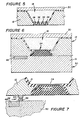
- FIG. 5 illustrates such a structure.
- the well 18 can be in the nature of a trench in which electrophoresis is carried out by providing a potential gradient along the length of the trench.
- Appropriate sensing electrodes 24 are speaced along the bottom of the trench whereby various species can be determined.
- Appropriate reference 36 and/or counter electrodes 42 are also provided along the bottom of the trench.
- Electronic circuitry 48 can advantageously be included in certain embodiments of the present invention in the substrate 12 adjacent the back surface 16 thereof.
- Such electronic circuitry 48 is adapted for, and serves for, processing signals from one or more of the sensing electrode 24, the reference electrode 36, and the counter electrode 42.
- the electronic circuitry 48 can be formulated by conventional integrated circuit fabrication techniques. Generally the circuitry will serve to convert the signals from high impedance to low impedance and may also amplify the signals from the electrodes, and, if desired, perform computational tasks and present the data in condition for display or printing out, for example as concentrations of the species being detected.
- the length(s) of the conductor(s) 26,40 and/or 46 in such instances can be kept extremely short leading to a very high signal-to-noise ratio and, therefore, increased sensitivity. Note also that the chemistry in the first well 18 is completely isolated from the electronic circuitry 48 whereby the integrity of the latter is protected.
- the electronic circuitry 48 can instead be on a separate semiconductor substrate 50 (see Figure 6) which abuts the back surface 16 of the substrate 12. This provides encapsulation and protection of the electronic circuitry 48.
- Figure 7 is an enlarged view of a portion of Figure 6. It illustrates the use of a bump bonding techniques to make the needed electrical connection between the conductor (26,20 and/or 46) and the electronic circuitry 48.
- the bump bonding site 52 is spaced from the electrode (24,36 and/or 42) whereby the contents of the cells (29,31,33) are not damaged by heat during bump bonding. Also, this allows good bump bonding contact to be made whereby the resulting bond has good mechanical strength.
- the bump bonding is carried out by pressing the bumps 54,56 together and heating the substrate 50.
- the bumps 54,56 can be of very different thickness. Good results have been obtained with the bump 54 of silver and about 2000 Angstroms thisck and with bump 56 of copper and about 10 microns thick.
- Figure 7 also illustrates the technique of providing the first electrode 24 by depositing a small amount of an electrode material, e.g., platinum, silver, etc., followed by depositing the first conductor 26,40,46.
- an electrode material e.g., platinum, silver, etc.
- the first electrode 24 forms a portion of the bottom 20 of the first well 18.
- a support material e.g., a polymer such as a polyimide.
- the reference electrode 36 is of the nature described above.
- the working or sensing electrode structure 24, on the other hand, is in the nature of an ion-selective membrane 58 (as described previously) covering a sensing electrode base 60 which is attached to a sensing conductor 62 in a passage 64 which leads from a bottom 66 of the sensing electrode well 18 to the back surface 16 of the substrate 12.
- the analyte medium makes the electrolytic contact between the ion-selective membrane 58 and the reference electrode 36.
- the barrier 30 is ion transparent or can be omitted.
- the electrolytic medium 39 is not the same material as is the ion-selective membrane 58.
- any of a number of ion selective membranes 58 can be used.
- such membranes are disclosed by M.A. Arnold and R.L Solsky Anal. Chem. 1986, 58, 84R - 101 R, M.E. Meyerhoff and Y.M. Fratecelli, Anal. Chem. 1982, 54, 27R - 44R, M.A. Arnold and M.E. Meyerhoff, Anal. Chem. 1984, 20R - 48R, and J. Koryta, Analytica Chimica Acta, 159, 1984, 1-46.
- each reference cell 31 is surrounded by, and can serve as the reference cell 31 for, several different sensing cells 29.
- sensing cell 29 on any substrate 12 more than one sensing cell 29 can be utilized for each chemical species being analyzed. That is, there can be two or five, or ten, or any desired number of sensing cells 29 which detect, for example, carbon monoxide. This provides extra selectivity by means of chemometrics, redundancy, and reliability in case any of the carbon monoxide sensing cells 29 fail whereby the electrode structure 10 would continue to operate.
- Chemometrics is the technique of mathematically treating data from a plurality of sensors to improve the selectivity of the analytical results (see, for example, Stetter, J.R., Jurs, P.C., and Rose, S.L., Anal. Chem. Vol. 58, pp 860-866 (1986)).
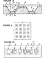
- Figure 10 illustrates an embodiment of the invention wherein a plurality of sensing cells 29 are provided, some of which can be for different constituents than others, e.g., oxygen, carbon dioxide and K + .
- a single reference cell 31 is also present as is a pressure sensor 70.
- the various cells 29,31 and the pressure sensor 70 are arranged linearly whereby the total lateral extension (width) of the array 72 of electrode structures 10 can be restricted to be no more than about 300 microns.
- the length of the array of the various cells 29,31 and the pressure sensor 70 is determined by the number of such cells (plus the pressure sensor 70) and can be restricted to be no more than about 150 microns multiplied by the number of cells plus the number of pressure sensors 70.
- the pressure sensor 70 can be a conventional piezoresistive-type pressure sensor of the nature described in, for example, Borky, J.M., IEEE Trans. On. Elect. Dev. Vol. ED-26, No. 12, December 1979.
- microelectronic chemical sensors allows the quantitative detection of different gases and organic vapors to further increase selectivity, to include redundancy, to increase reliability, and to permit use of chemometrix. Also, it is possible to include different types of sensors within such an array. For example, the internal temperature of a sensor can be monitored to compensate for known parameter changes with temperature. Also, a microhumidity sensor can be incorporated.
- Each microelectronic chemical sensor can comprise a different electrocatalyst coating so that each sensor is as specific as possible to a certain gas or vapor.
- a sensor comprising an array of optimized microsensors exhibits a maximum selectivity to a given mixture of gases and/or vapors.
- the presence of extra sensor elements with the same configuration and catalysts allows not only for averaging the signals of identical elements but also for correcting signals of dissimilar elements.
- Unraveling vapor spectral data from an array of microsensors in a gas or vapor detection system is possible with a microcomputer that uses innovative signal-processing techniques to overcome inherent limitations of the single sensor elements. Pattern-recognition methods can be used to determine the uniqueness of the information obtained and the capacity of each of the channels for classification. Recently, such a pattern recognition analysis of data from an electrochemical sensor array has been successfully applied for the detection of hazardous gases and vapors (Stetter, Jurs and Rose, 1986).
- the array containing n individual sensors that are operated amperometrically yields n channels of data for an unknown chemical species detected.
- the n-channels sensor responses for each compound are normalized so that the strongest channel equals 1 (or -1, if a negative number).
- This normalized set of response is termed a pattern vector as follows:
- Figure 11 illustrates a portion of the embodiment of the linear array of Figure 10 and shows the structure of the pressure sensor 70.
- a flexing membrane 71 which can flex into a cavity 73 between a support 75, which may be made of any convenient material, e.g., glass, plastic or a semiconductor such as silicon.
- Element P is the pressure element.
- Piezoresistors can be diffused in the back of the thin silicon membrane and all electronics are protected with, for example, a Mallory bonded glass piece (the support 75).
- the cavity 73 in the support 75 provides space for the electronics and can be evacuated to make an absolute pressure sensor possible.
- Figure 12 shows an embodiment of the invention wherein each of the sensing electrode 24 and the counter electrode 42 are in the first well 18.
- the reference electrode 36 communicates with the first well 18 via a pinhole 76 whereby the chemistry of the reference electrode cell 31 is kept separate from but communicates electrically with the electrolytic medium 28 in the first well 18.
- the reference electrode 36 is adjacent the back side 16 of the substrate 12 and is closed off by an enclosure 78 which may be merely an extension of the reference electrode 36, or which can alternatively be of a different material.
- the original filling of the reference cell 31 is from the back side 16 of the substrate 12.
- Figure 13 shows an embodiment of the invention wherein the sensing and counter electrodes 24,42 are in a single well 79, while the reference electrode 36 is in a separate well 81.
- An appropriate salt bridge 83 or its equivalent, provides ionic conductance between the electrolytic mediums 28 and 39. This is a typical structure for conductometric and voltammetric measurements, for example, a Clark oxygen sensor.
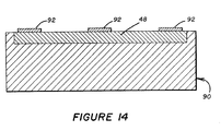
- the electronic circuitry 48 on a separate member 90 (see Figure 14) which, via appropriate contacts 92 can form temporary electrical contact with the appropriate conductors 26,40 and/or 46 (for example, as seen in Figure 2) during determination of the concentration or presence of one or more species.
- a single member 90 can provide the needed electronic circuitry 48 for a plurality of electrode structures 10. Also, if the electrode structure 10 is used in an environment where it must be more or less permanently installed and where it has only a short useful lifetime, only the electrode structure 10 need be replaced and not the electronic circuitry 48 (since the latter need only be exposed to the environment during the actual time of measurement).
- the first well 18 can be made any convenient depth. It is preferred that the first well 18 extends sufficiently towards the back surface 16 of the substrate 12 whereby the first electrode 24 is sufficiently deeply positioned within the first well 18 whereby electrochemical reaction of the selected moiety at the first electrode 24 provides a substantially Nernstian slope. In general, this means that the first well 18 should be sufficiently deep so that the electrolytic medium 28 (when present), or the membrane portion of the ion-selective electrode (when present), while remaining entirely within the first well 18, extends above the first electrode 24 a distance of at least about 40 microns.
- the first well 18 extends towards the back surface 16 of the substrate 12 from about 40 to about 200 microns.
- the back surface 16 of the substrate should be close enough to the bottom of the well so that shunting does not occur between respective conductors.
- the back surface 16 can be from about 10 to about 100 microns from the first well bottom 20. This assures very short contacts and also allows inexpensive anisotropic etching techniques (which provide tapered passages, as illustrated) to be used to form the first passage 22, and, if necessary, the second passage 38 and/or the third passage 44.
- the etching is anisotropic in such an instance the widths of the passages 22, 38 and 44 at the back surface 16 could otherwise become so wide that the conductors 26, 40 and/or 46 met before or at the back surface 16. If laser drilling is used to form the passages 22,38 and/or 44 this problem does not exist but laser drilling will not produce as many cells per unit time since either the laser must be repositioned to drill each passage.
- the sensor well 18 extends from about 60 to about 125 microns towards the back surface 16 and it is preferred that the back surface 16 is from about 10 to about 40 microns from the sensor well bottom 20.
- a particularly preferred structure is one wherein the sensor well 18 is approximately 100 microns deep and the back surface 16 is about 25 microns from the sensor well bottom 20. The same preferences hold with respect to the size of the reference well and the counter well, if such is present.
- a thinner electrolytic medium 28 over the sensing electrode 24 can be more appropriate, for example, between 20 and 50 microns.
- the first well 18 and other wells as well can be only partially filled with the appropriate electrolytic medium 28,39,41.
- the pH response of an lrO 2 electrode was tested in physiological saline solution in the pH range 6.0 - 8.0.
- the measuring cell consisted of a 1 ⁇ m thick IrO 2 electrode separated from a Ag/Cl electrode by 50 ⁇ m.
- the electrodes were fabricated on the surface of a silicon substrate coated with silicon dioxide. Adhesion layers were used of 100 Angstroms Ti for IrO 2 and 50 Angstroms each of Ti and Pd for Ag.
- AgCI was formed by bringing Ag in contact with a 1% FeC1 3 solution for two minutes. The potential of the Ag/AgCI electrode was first checked against a saturated calomel electrode and it agreed with the literature value. The response of the IrO 2 electrode was then measured using this Ag/AgCl electrode reference.
- the lr0 2 electrodes of Example 1 which gave near-Nerstian response were used in the fabrication of C0 2 electrodes.
- a 5% solution of poly(hydroxy ethyl methacrylate) in 950/0 ethanol was painted onto the IrO 2 -AgAgCl electrode area. The solvent was allowed to evaporate.
- the dried polymer was equilibrated with 10- 3 M NaHC0 3 + 0.1 M NaCI.
- the gel and the electrolyte were then allowed to dry up. 4.75% polysiloxane-polycarbonate solution was painted on top of the gel. Again, the solvent was allowed to dry completely.
- the completed electrode was checked for its response to C0 2 . Different concentrations of C0 2 were generated by adding known volumes of 0.1M NaHC0 3 solution to 0.1M HCI. It was assumed that all NaHCOs was converted to C0 2 .
- the change in potential of the electrodes was as follows:
- the response time of the electrode was approximately 60 seconds.
- the response time and detection limit can be improved by controlling the thickness of the polymer membrane and the composition and thickness of the hydrogel. No attempt was done to optimize them in the planar structure.
- the senor was completed by casting a silicone/polycarbonate membrane over the whole structure. It was observed that the electrode decreased after this step.
- a practical example of the current invention is a sensor for pH, C0 2 and 0 2 in blood.
- the sensing well 29 which is intended for pH sensing has besides the general outlook of Figure 4 the following specifics.
- One electrode in the pH sensing well 29 consists of iridium dioxide and one electrode consists of Ag/AgCI.
- the lr0 2 electrode is made by reactive sputtering through a silicon mask from the back of substrate 12.
- a promotion layer titanium is also sputtered on, as well as an iridium layer to make a better performing iridium/iridum dioxide electrode.
- Ag is used to back up these layers.
- the order of the depositions just mentioned is as follows:
- the oxygen electrolytic sensing cell 29 is made in one of two fashions:
- the material of the barrier 30 identified as a good choice for the C0 2 and 0 2 element is a block copolymer of polycarbonate with silicone rubber.
- This product e.g., General Electric MEM-213
- MEM-213 can be heat sealed and is heat shrinkable. It can be easily solution cast.
- the solvents used to cast this membrane are, for example, toluene or dichloromethane.
- the membrane can be locally laser cut or it can be locally dissolved.
- the C0 2 cell 29 contains the same electrodes as the pH cell 29 except that in this case we do have an electrolytic medium, a buffer, covered by the same membrane as mentioned with respect to the oxygen cell.
- the present invention provides a microelectrochemical electrode structure 10, and arrays thereof on a substrate 12.
- Such electrode structure 10 and arrays of electrode structures 10 on a single substrate 12 are useable for detecting low concentrations of gaseous, ionic and nonionic species.
Abstract
Description
- The present invention relates to microelectrochemical sensors useful for detecting various chemicals, including vaporous and gaseous species and dissolved species, in very low concentrations. The micro-electrochemical sensors themselves are formulated by integrated circuit (IC) engineering techniques and can be extremely small in size, namely, as small as one-fifth to one-sixth the size of the smallest previously known sensors. Among numerous other uses, they may be utilized to analyze blood chemistry, in vivo.
- In a large number of situations it is desirable to be able to analyze a sample, be it a liquid sample or a gaseous sample, for one or more constituents. Often, it is desirable to analyze for several constituents at once. For example, it is desirable to be able to analyze blood for such diverse components as H+, K+, C02 and 02, etc. It is also often desirable to be able to analyze air samples for air borne contaminants such as CO, NO, N02, N20, S02, H2S and 02 and other gases as well.
- Within the last several years a number of sensors have been developed based upon one or more of the techniques developed by integrated circuit engineering technology. For example, U.S. Patent 4,020,830, issued May 3, 1977 to C.C. Johnson, et al, utilizes a chemical sensitive field-effect transistor (FET) transducer for selectively detecting and measuring chemical properties of substances to which the transducer is exposed. Basically, the chemical being detected interacts with certain substances to modulate the electric field produced in the substrate semiconductor material between diffusion regions thereof. Such FET devices have been demonstrated to be useable for detecting ions as well as gases, and indirectly certain dissolved molecules. However, fluctuations in drain current leading to errors are still a significant problem These fluctuations can be associated with thermal noise or they can be light induced. Layers that make the FET chemically sensitive and selective are very difficult to deposit on the gates of such devices, especially since often several layers of different composition are needed. All of this leads to errors or makes fabrication difficult Still further, reference electrodes are very difficult to implement in FET structures.
- S.J. Pace, as set forth in U.S Patent 4,225,410, discloses a disposable integrated miniaturized array of chemical sensors for analyzing concurrently a number of analytes in a fluid sample. Each sensor of the array is a complete electrochemical cell having its own reference and indicator electrodes and is selective with respect to a particular analyte, The sensors are all formed on top of the surface of a substrate which is prepared by press forming powdered alumina with appropriate through holes and imprints for the electrochemical circuit. Because of the manufacturing techniques such sensors and sensor arrays must be relatively large and are more properly describable as minisensors rather than microsensors.
- In U.S. Patent 4,549,951, issued October 29,1985 to M.B. Knudson, et al, a relatively large, compared to both of the devices discussed above, ion selective electrode is set forth which is used along with a separate reference electrode. The ion-selective membrane of the electrode sits on a conductor embedded in a plastic substrate, This is basically a small ion-selective electrode with the membrane sitting on top of a conductor and without an internal reference electrolyte or true reference electrode. Further, construction of such an electrode design in micro sizes appears to be beyond the current state of the art.
- In the devices of U.S. Patents 4,020,830, 4,225,410, and 4,549,951 the entire electrochemical cell sits upon the surface of a substrate. This leads to a significant problem in providing proper encapsulation. In the case of U.S. Patent 4,020,830, all of the electronic circuitry is included on the analyte detecting side of the FET. This leads to problems between the chemicals and the electronic circuitry which are either in contact with one another or closely adjacent to one another.
- The prior art, including the above discussed patents, does not yet provide microelectrochemical sensors and sensor arrays incorporating both amperometric and potentiometric elements, which operate at room temperature and consume little power, which provide versatile, multi-purpose-multi-channel, real time monitoring of vapors, gases, molecules and ions, which are micro-portable and field rugged, which have fast response times at ambient temperature, which are free of interferences from such parameters as oxygen deficiency and humidity, which can be produced inexpensively using sophisticated modern micro-fabrication technologies, which have high specificity and high selectivity, for example, parts-per-billion level detection of such gases CO, NO, N02, H2S, S02, and N2H4 and parts-per-million detection of such gases as HCN, C12, H2, 02, C2HsOH, HCHO, C3H3N, 03, C2H2, C2H4, CH4, C2H6, C3H8, and organophosphate vapors, and which are adaptable for detecting ionic electroactive species in parts-per-billion in solutions, including, for example, CI-, Br, I-, SCN-, CN-, S203 2-, OCI-, S03 2-, phenols, aromatic amines, nitro compounds, organoarsines, and metal ions, e.g., CU2+, Fe3+.
- The present invention is directed to solving one or more of the problems as set forth above.
- In one embodiment of the present invention a microelectrochemical electrode structure is set forth. The aforementioned electrode structure comprises a monolithic substrate having a front surface and a back surface facing generally away from one another. A first well extends into the substrate from the front surface towards the back surface and ends in a first well bottom. A first passage extends into the substrate from the back surface to the first well bottom. A first electrolytic cell including a first electrode is located wholly between the front and back surfaces of the substrate. A first conductor is located in the first passage and electrically communicates the first electrode to adjacent the back surface.
- In accordance with one embodiment of the invention an electrolytic medium is in the first well. A barrier covers the first well, the barrier having an outfacing surface and an infacing surface. The infacing surface is in flow contact with the electrolytic medium. The barrier provides entry into the electrolytic medium of a selected moiety in response to contact of a selected species with the outfacing surface. The barrier is at least substantially impermeable to the electrolytic medium.
- Another embodiment of the present invention is a sensor array including a plurality of such first electrode structures in the substrate.
- Optionally, each electrode structure can have more than one electrode in the first well.
- An electrode structure in accordance with the present invention is characterized by extremely small size, is operable at room temperature, utilizes low power, is field rugged, has a fast response time, is not sensitive to interferences due to oxygen deficiency or differences in humidity, can be readily mass produced using sophisticated microfabrication technologies, has high specificity and high selectivity, can have very short signal lines to signal amplification circuitry integrated and embedded in the back side of the substrate thereby providing a high signal-to-noise ratio, and is useful in accordance with specific embodiments to detect vapors, dissolved ions and dissolved nonionic species (including dissolved gases). The structure is also very well suited to having a pressure element incorporated in an array therewith. Because the geometric configuration of a resistive or capacitive sensor is so similar to the structure created for the chemical sensitive elements it only requires a few more processing steps to also include a pressure element on the same substrate. In some applications (e.g., biomedical) such added features are very beneficial.
- In accordance with embodiments of the present invention a single substrate can have an array of one or more electrode structures, each sensitive for one or several of a number of different chemical species. And, the entire sensor array can be so small that it can be readily positioned in, for example, a catheter in the blood stream and can be used to give a constant readout of such chemicals as C02, 02, K+, H+, and the like. In accordance with certain embodiments of the present invention it is possible to include integrated circuitry electronics on the back surface of the substrate removed from the electrochemistry whereby one can amplify the signals and/or obtain electrical output signals which are specifically indictive of the concentration of one or of a number of species. The electrode structure of the present invention can be designed to exhibit substantially Nernstian slopes for ionic species. The amperometric electrode structures of the present invention can be designed to exhibit substantially linear dependency on concentration. The bottom of the first well can be chosen to be at different distances from the front and back surfaces of the substrate for different intended applications.
- The invention will be better understood by reference to the figures of the drawings wherein like numbers denote like parts throughout and wherein:
- Figure 1 illustrates, in a side sectional view, an embodiment of a microelectrochemical sensor in accordance with an embodiment of the present invention;
- Figure 2 illustrates, in similar view, an alternate embodiment of the present invention;
- Figure 3 illustrates, in similar view, an alternate embodiment of the present invention;
- Figure 4 illustrates, in similar view, an alternate embodiment of the present invention;
- Figure 5 illustrates, in similar view; an alternate embodiment of the present invention;
- Figure 6 illustrates, in similar view, an alternate embodiment of the present invention;
- Figure 7 illustrates a detail in the embodiment of Figure 6;
- Figure 8 illustrates, in similar view, an alternate embodiment of the present invention;
- Figure 9 illustrates, in plan view, an array of microelectrochemical sensors in accordance with an embodiment of the present invention;
- Figure 10 illustrates, in plan view, an alternate array of microelectrochemical sensors in accordance with an embodiment of the present invention;
- Figure 11 illustrates a side sectional view of a portion of Figure 10 and shows the combination of an array of sensor elements with a pressure sensor;
- Figure 12 illustrates, in similar view to Figure 1, an alternate embodiment of the present invention;
- Figure 13 illustrates, in similar view to Figure 1, an alternate embodiment of the present invention; and
- Figure 14 illustrates, in a side sectional view, a separate electronics containing member useful in an alternate embodiment of the present invention.
- The present invention provides a
microelectrochemical electrode structure 10 including an electrolytic cell 11, one embodiment of which is illustrated in Figure 1. Theelectrode structure 10 includes amonolithic substrate 12 having afront surface 14 and aback surface 16 facing generally away from one another. Thesubstrate 12 can be made of any of a number of materials but it is particularly advantageous to make thesubstrate 12 out of a semiconductor material such as silicon, silicon carbide, gallium arsenide, or the like. The invention, however, is more general in that thesubstrate 12 may also be made of a plastic material, a refractory oxide, or substantially any other material. It is even possible to make thesubstrate 12 of a conductive material, but in such an instance, and generally in instances in which thesubstrate 12 is made of a semiconductor material, it is necessary to provide an appropriate insulatinglayer 13 to prevent shorting through thesubstrate 12. For example, asilicon dioxide layer 13 can be formed by contacting a silicon substrate with wet oxygen at elevated temperature, e.g., about 1000°C. - It is important that the
substrate 12 be monolithic i.e., a unitary structure formed of a single material, as this allows particularly easy construction and eliminates or greatly reduces problems of prior art devices. Particular problems which are eliminated or greatly reduced include: (1) securing various chemistries to the electrodes especially when multilayered structures are required; (2) affixing the membranes that cover the chemistries in the wells; (3) leakage of electrolyte to the electronics; (4) the depositing of thick electrolytic mediums which are sometimes necessary; (5) encapsulation problems; (6) light sensitivity problems; (7) lack of versatility to do, for example, current as well as voltage measurements; (8) high cost; (9) incompatibilities of various chemistries with IC processing. - The electrochemical analysis which can be made in accordance with the methods of and/or using the sensors of the present invention includes voltammetric, potentiometric, coulombic, conductometric and AC analysis.
- These problems exist for several reasons. First, the prior art devices build walls upwardly from a surface and the build up must be high enough to contain the chemistry. Second, encapsulation is difficult since the electronics are at the same surface as are the chemistries. Third, the gates of FET devices are exposed to light to which they are sensitive. Fourth, the electrolyte, being adjacent the electronics, can leak into the electronics. Fifth, since the electronics and chemistries are on the same surface the use of simple bump bonding techniques to connect sensors with electronics is precluded.
- In accordance with the present invention a
first well 18 extends into thesubstrate 12 from thefront surface 14 and extends towards theback surface 16. All of the needed chemicals of the cell 11 are within thefirst well 18. Thefirst well 18 ends in afirst well bottom 20. Afirst passage 22 extends into thesubstrate 12 from theback surface 16 to the first well bottom 20. Thefirst well 18 can be formed by any of a number of techniques, including, particularly, anisotropic etching carried out in accordance with the techniques of the semiconductor industry (in which instance the (100) face of the silicon corresponds to the front surface 14). Such a process includes such steps as cleaning thesubstrate 12, applying a photoresist layer, prebaking the layer, exposing the photoresist, developing the photoresist, rinsing thesubstrate 12, drying thesubstrate 12, and post baking it. Methods for carrying out each of such steps are known in the IC art and descriptions of such techniques may be found in, for example, "Integrated Circuit Engineering" by A.B. Glaser and G.E. Subak-Sharpe, Addison-Wesley Publishing Company, Reading, Massachusettes, 1977. In this same text are found explanations of etching, oxidation of silicon, formation of a silicon nitride insulating layer, and the like. An alternative way of forming well 18 (andpassage 22 as well) is by laser drilling. Holes of various forms with lateral extensions from a few microns to hundreds of microns can be formed by this method. Depending on the depth, a process time, per hole formation, of less than 1 second can be involved. The silicon wet anistropic etching technique has two major advantages over laser drilling. One, it is a parallel process whereby many holes can be made at once. Two, the surfaces are smooth and very well defined. The advantage of laser drilling is that it can provide straight but not smooth walled holes when such are desirable. - In accordance with an embodiment of the present invention a
first electrode 24 is provided which is, very importantly, wholly between thefront surface 14 and theback surface 16 and which extends at least to thefirst well 18. This is very important as this enables the securing of subsequent layers in a straight-forward fashion, makes the accommodation of the electrolytic medium in general easier (for example, eliminates spilling using an ink jet printer type of chemistry filling device), and allows for an easier fixing of additional barriers. Also better encapsulation is provided. - A
first conductor 26 is provided in thefirst passage 22 and serves for electrically communicating thefirst electrode 24 to adjacent theback surface 16 of thesubstrate 12. Thefirst conductor 26 is suitably an electronic, as opposed to an ionic, conductor. Alternatively, a well facing end 27 of theconductor 26 can play the role of theelectrode 24. This feature makes the fabrication of thesensor 10 dramatically simpler. Often, however, the sensor electrode metal will need additional backup layers (e.g., aluminum or titanium) for strength and/or economy. - The
first passage 22 can be made by any of the known techniques of the semiconductor art. For example, such techniques as anisotropic etching, laser drilling, aluminum thermomigration, and the like are useful. Thefirst conductor 26 can be provided in thefirst passage 22, again by the techniques of the semiconductor art. For example, thefirst conductor 26 can be provided by such techniques as aluminum thermomigration, metal deposition, (evaporation or sputtering), electroless plating, electron beam evaporation, mechanical positioning of metal rods, melting in place with vacuum application, or the like. Aluminum thermomigration is a useful technique to make the metal contacts. This technique has the advantage of providing the hole and conductor in a single operation. In practice, however, the thermomigration technique is quite difficult and wet anistropic etching followed by metal deposition is currently preferable. - Various types of
electrode structures 10 can be formed These include, for example, the Ag/AgCI reference electrode, platinum, platinum black, silver, gold, iridium, palladium, palladium/silver, iridum dioxide, platinum black/paladium, platinum oxide, and mixtures thereof, electronically conductive polymers, and generally any of the electrodes normally utilized in electrochemical measurements. Table 1 sets forth, as examples only, a short list of gases, and electrochemical systems which have been used to determine them. - In certain embodiments of the invention an
electrolytic medium 28 is provided in thefirst well 18. Theelectrolytic medium 28 can be a liquid but more preferably is in the nature of a hydrogel, a plasticized polymeric membrane for potentiometric elements, an ion selective membrane, or a solid polymer electrolyte. - The needed materials for the
various electrode structures 10 can be placed in theappropriate wells 18 as follows: pure metals if they need to be deposited from the front can be sputtered or evaporated, electron-beam or ohmic evaporation may be used, insoluble deposits of metal salts can be formed by chemical or electrochemical treatment of metals in situ. They can be deposited from the back as previously set forth. For providing the hydrogel one has the choice of lift off technology or ink-jet printer like technology. Solid polymeric electrolytes can be put in place in the same manner as hydrogels. Also, ion-selective membranes can be placed in the appropriate well(s) in the same manner as can hydrogels. Further, liquid membranes can be provided in the same manner. Composite membranes, which include enzyme based membranes, tissue cultures, living organisms, antigen-antibody and generally biocatalyst materials can also be placed in the well in the same manner. - In prinpiple, all gases or vapors that can be electrochemically oxidized or reduced can be sensed by limiting current measurement using amperometry. The reactions occur at a characteristic potential at the electrode/electrolyte interface. An appropriate potential at which only the desired reaction proceeds must be applied to the electrode so as to obtain potential-controlled selectivity. Selectivity (or the ability to observe only one of the many possible reactions) can be either kinetic or thermodynamic in origin. Thus, the selectivity is a function of the sensing electrode catalyst and (material) potential.
- An approximate indication of the suitable range of potential is provided by the reversible potentials of the reaction involved; some values are listed in Table 2. Note that each gas reaction exhibits a characteristic thermodynamic potential. An example of thermodynamic selectivity is the reduction of N02 that occurs at low potentials (Sedlak and Blurton, 1986).


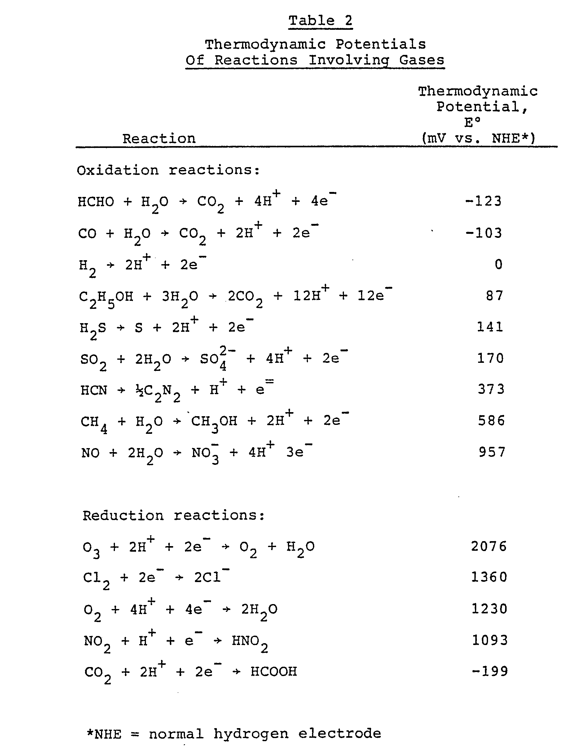
- Because N02 is reduced to NO and the NO product is not further reduced, the N02 sensor (with sensing electrode operated at low potentials) is selective for N02, having no signal for the NO that may be present. This N02 selectivity results from control of the sensing electrode's potential in a range such that no NO reactivity is observed. The potential of the electrochemical cell has been compared to the temperature of a catalyst surface (Blurton and Stetter, 1977), which also may be used for control of the catalyst reactivity. Control of the potential is accomplished in many sensors by using three electrodes and a potentiostatic circuit.
- More exact information as to a suitable range of potentials is afforded by the kinetics of the oxidation or reduction reaction, which can be discussed only in terms of electrocatalysis. Each electrocatalyst formulation will have unique properties. The activity of platinum for CO oxidation has been found to be 103 to 106 times better than that of gold. This is a good example of kinetic selectivity. Both reactions occur on both metals, but one is orders of magnitude more rapid than the other. Although the presently available sensors utilize expensive, noble metal catalysts, the required amount of such a catalyst for each sensing element in
electrode structures 10 in accordance with the present invention is minimal because the sensor is a microsize device. Moreover, inexpensive electrocatalysts based on polymer materials that exhibit catalytic activity and selectivity as high as those of noble metals can be used in place of the noble metals. - If the gas to be sensed exists in a mixture containing several reactive components that exhibit close thermodynamic selectivity potential (cf. Table 2), the concentration of the desired component can be determined selectivity by the differential pulse voltammetry (DPV) technique. Let us consider a simple example where a mixture of Gas A and Gas B exists. Gas A and Gas B would exhibit current vs. potential curves with different limiting currents IA and IB. By differentiating these curves, one obtains two sharp clearly separated peaks with different characteristic potentials, EA and Es. The peak current values are proportional to the gas concentrations. Thus, the DPV technique, in addition to an improved signal-to-noise ratio, can provide potential-controlled selectivity to an electrochemical sensor through precise measurements of Epeak values, which are closely related to the thermodynamic potentials given in Table 2 and are characteristic to each gas species.
- Among useful electrolytes, particularly for amperometric elements are solid electrolytes, including solid polymeric electrolytes such as Nafion (a trademark of DuPont) which is part of a class of solid polymeric ion exchangers which conduct ions upon exposure to water. Probably the best known examples are membranes made from polystyrene with fixed negative sites (sulfonate, carboxylate or phosphonate) or fixed positive sites (quaternary ammonium or quaternary phosphonium). Selection as far as ions are concerned with these materials is almost exclusively on the basis of charge and for ions with the same charge discrimination is very slight. For amperometric sensing the use of these materials is relatively new. Other examples of solid polymeric electrolytes besides Nafion (which a is perfluorinated ionomer) are sulfonated styrene-divinyl benzene resins and divinyl napthalene sulfonic acid polymer.
- Such polymers are characterized chemically and physically in that they have a hydrophobic nature with ionic (hydrophilic) clusters inside. They conduct ions upon hydration. They exclude co-ions up to the Donnan failure point at which stage ions of both types can penetrate into the resin. Neutral molecules can diffuse readily through such membranes and especially large organic molecules can dissolve within the more hydrophobic resins.
- Resins can also be used as reference solutions (see, for example, French patent publication No. 2,158,905). These ion exchange resins have been used as the electrolytic medium for a potentiometric C02 sensor (see, for example, U.S. Patent 3,730,868).
- For potentiometric elements membranes can comprise a polymeric binder or support impregnated with a solution of an ion selective carrier or ionophore in a solvent for the ionophore. Membranes of this type can be tailored to sense particular ions selectively. For example, for sodium the antibiotic nonactin can be used as the ionophore in a PVC matrix plasticized with dioctyl sebacate. For potassium, valinomycine would replace the nonactin.
- Useful gels for incorporation within the sensor structure include, without limitation: methylcellulose, polyvinyl alcohol, agar, carboxycellulose, gelatin, agarose, deionized gelatin, polyacrylamide, polyvinyl pyrrolidone, hydroxyethylacrylate, hydroxyethylmethacrylate, and polyacrylic acid. They are characterized in that they constitute thickened (more viscous) solutions. They are hydrophilic in natural and include synthetic polymeric film forming materials.
- In certain cases the
electrolytic medium 28 can come from a solution being analyzed. In most cases where theelectrolytic medium 28 is present, however, it is provided during the construction of theelectrode structure 10. Often it will be undesirable to allow a solution being analyzed to mix with and/or directly contact theelectrolytic medium 28. - A
barrier 30, generally in the nature of a membrane, can cover thefirst well 18. Thebarrier 30 has an outfacingsurface 32 and aninfacing surface 34 and theinfacing surface 34 is in f!ow contact with the electrolytic medium 28 so as to provide a full conductive path. Indeed, thebarrier 30 can be at least partially within thefirst well 18. Thebarrier 30 provides entry into theelectrolytic medium 28 of a selected moiety in response to contact of a selected species with the outfacingsurface 32 of thebarrier 30. Either the selected species will pass through thebarrier 30 and will then constitute the selected moiety, or contact of the selected species with thebarrier 30 will lead to the introduction of a different moiety into theelectrolytic medium 28. Thebarrier 30 is generally at least substantially impermeable to the electrolytic medium 28 to prevent escape and/or mixing with the analyte solution exterior of thebarrier 30. Thebarrier 30 would not be present, or would be permeable to a solution being analyzed, in those instances when the solution constitutes theelectrolytic medium 28. - The
barrier 30 may encapsulate theentire electrode structure 10 including thefront surface 14 and theback surface 16. Alternatively, thebarrier 30 may only cover thefirst well 18, or thefirst well 18 and part or all of thefront surface 14. It may be desirable to encapsulate the remainder of theelectrode structure 10, or even all of theelectrode structure 10 including thebarrier 30, as a protection against contamination. Generally, an inert encapsulating layer (not shown) will serve the purpose. The encapsulating layer, when present, must provide access (via, for example, pores or holes therethrough) to thefirst well 18 or to thebarrier 30 covering thefirst well 18. It can be formulated as can thebarrier 30. - A number of materials may serve as the
barrier 30. For example, thebarrier 30 can comprise a gas pervious liquid impervious membrane. This is useful in the situation wherein the sensor is used in a liquid to detect dissolved gases, for example, if theelectrode structure 10 is utilized in blood. - Other types of materials for utilizing as the
barrier 30 are teflon membranes, silicone rubber membranes, silicon polycarbonate rubber membranes, mylar, nylon 6, polyvinyl alcohol, polyvinyl chloride, methylcellulose, cellulose acetate, high density polyethylene, polystyrene, natural rubber, fluorosilicone, dimethylsilicon rubber, any appropriately perforate photoresist polymer, and dimethylsilicon. It is generally preferred that the membranes utilized be solution castable so as to make fabrication of the membrane more easily accomplished. - The
barrier 30 can be placed over appropriate of thewells 18 by, for example: solution casting, separate casting on a different substrate and physical transfer, heat shrinking in place, solution casting utilizing an ink-jet printer, spin coating, or dip coating. If the barrier is in the nature of uniform latex microspheres, made for example of polystyrene, styrene-butydiene, or teflon, such microspheres can be placed in position utilizing the ink-jet technique, by dipping, by solvent spraying, or the like. If the barrier is of the nature of or includes activated carbon or similar materials it can be placed in position by ink-jet printing, solvent casting, or the like. If the barrier includes, for example, permanganate coated alumina or other substance which serves to remove nitric oxide, it can be placed in position similarly to the carbon particles. - The
microelectrochemical electrode structure 10 just described may serve as a working or sensing electrode, a reference electrode, or a counter or auxiliary electrode. As may be seen in Figure 2 asingle substrate 12 may have one or more each of asensing electrode cell 29, areference electrode cell 31, and acounter electrode cell 33 thereon with appropriate provision, e.g.,salt bridges electrolytic mediums barrier 30 is a barrier for all ions. - Note that the designations S, R and C are used in the figures to indicate, respectively, sensing, reference and counter electrodes.
- If the
first electrode 24 is a sensing electrode thesubstrate 12 will also include areference electrode 36 in ionic electrical communication with thefirst electrode 24. Thereference electrode 36 will also be electrically isolated from thesensing electrode 24 other than via theelectrolytic medium 28. For example, if the substrate is silicon an appropriate silicon dioxide orsilicon nitride layer 13 can be conventionally deposited or formed in thefirst well 18 and in thefirst passage 22. Thereference electrode 36 can also be provided with its own different electrolytic medium 39 (Figure 2) containing the species which determine the reference electrode potential. Also, thecounter electrode 42 can be provided with a separate electrolytic medium 41 (Figure 2). In the embodiment illustrated in Figures 3 and 4 thesensing electrode 24 and thereference electrode 36 are each in thefirst well 18. In such an instance thesubstrate 12 has asecond passage 38 extending from theback surface 16 of thesubstrate 12 to thereference electrode 36 in the first or sensor well bottom 20. Asecond conductor 40 is in thesecond passage 38 and serves for electrically communicating thereference electrode 36 to adjacent theback surface 16 of thesubstrate 12. If the substrate is silicon the silicon dioxide orsilicon nitride layer 13 also extends along thesecond passage 38. - A
counter electrode 42 is provided in those instances when such is necessary, for example, for making non-potiometric measurements. The counter electrode 42 (see Figure 3) is in ionic electrical communication with theelectrolytic medium 28 and is electrically isolated from thesensing electrode 24, and from the reference electrode 36 (when such is present), other than via theelectrolytic medium 28. Thecounter electrode 42 may be in thesame well 18 as is thesensing electrode 24, as illustrated, for example, in the embodiments of Figures 3 and 4. And, thecounter electrode 42 can, be in the same well as is thereference electrode 36 as in the embodiment of Figure 3. Thecounter electrode 42 may be in thesame well 18 as is thesensing electrode 24, that is it may be in thefirst well 18. This embodiment is seen in Figures 3, 4, 11, 12 and 13. In the structure of Figure 3 thesubstrate 12 has athird passage 44 extending from theback surface 16 thereof to the first well bottom 20. Athird conductor 46 is located in thethird passage 44 and electronically communicates thecounter electrode 42 to adjacent theback surface 16 of thesubstrate 12. - In the case of Figure 4 the
counter electrode 42 also plays the role ofreference electrode 40. The silicon dioxide orsilicon nitride layer 13 provides needed insulation. - In certain instances, for example, AC measurements, conductometric measurements, and the like, it may be desirable to have more than three electrodes in a
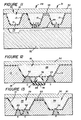
single well 18. Figure 5 illustrates such a structure. In a particular instance (not shown) the well 18 can be in the nature of a trench in which electrophoresis is carried out by providing a potential gradient along the length of the trench.Appropriate sensing electrodes 24 are speaced along the bottom of the trench whereby various species can be determined.Appropriate reference 36 and/orcounter electrodes 42 are also provided along the bottom of the trench.Electronic circuitry 48 can advantageously be included in certain embodiments of the present invention in thesubstrate 12 adjacent theback surface 16 thereof. Suchelectronic circuitry 48 is adapted for, and serves for, processing signals from one or more of thesensing electrode 24, thereference electrode 36, and thecounter electrode 42. Theelectronic circuitry 48 can be formulated by conventional integrated circuit fabrication techniques. Generally the circuitry will serve to convert the signals from high impedance to low impedance and may also amplify the signals from the electrodes, and, if desired, perform computational tasks and present the data in condition for display or printing out, for example as concentrations of the species being detected. The length(s) of the conductor(s) 26,40 and/or 46 in such instances can be kept extremely short leading to a very high signal-to-noise ratio and, therefore, increased sensitivity. Note also that the chemistry in thefirst well 18 is completely isolated from theelectronic circuitry 48 whereby the integrity of the latter is protected. - As an alternative to having the
electronic circuitry 48 on the back surface of thesubstrate 12, theelectronic circuitry 48 can instead be on a separate semiconductor substrate 50 (see Figure 6) which abuts theback surface 16 of thesubstrate 12. This provides encapsulation and protection of theelectronic circuitry 48. - Figure 7 is an enlarged view of a portion of Figure 6. It illustrates the use of a bump bonding techniques to make the needed electrical connection between the conductor (26,20 and/or 46) and the
electronic circuitry 48. The bump bonding site 52 is spaced from the electrode (24,36 and/or 42) whereby the contents of the cells (29,31,33) are not damaged by heat during bump bonding. Also, this allows good bump bonding contact to be made whereby the resulting bond has good mechanical strength. Basically, the bump bonding is carried out by pressing thebumps substrate 50. Thebumps bump 54 of silver and about 2000 Angstroms thisck and withbump 56 of copper and about 10 microns thick. - Figure 7 also illustrates the technique of providing the
first electrode 24 by depositing a small amount of an electrode material, e.g., platinum, silver, etc., followed by depositing thefirst conductor first electrode 24 forms a portion of the bottom 20 of thefirst well 18. Also illustrated is filling in thepassage - In accordance with one embodiment of the present invention, for example, as illustrated in Figure 8, the
reference electrode 36 is of the nature described above. The working or sensingelectrode structure 24, on the other hand, is in the nature of an ion-selective membrane 58 (as described previously) covering asensing electrode base 60 which is attached to asensing conductor 62 in apassage 64 which leads from a bottom 66 of the sensing electrode well 18 to theback surface 16 of thesubstrate 12. The analyte medium makes the electrolytic contact between the ion-selective membrane 58 and thereference electrode 36. In this instance thebarrier 30 is ion transparent or can be omitted. Note that theelectrolytic medium 39 is not the same material as is the ion-selective membrane 58. - Any of a number of ion
selective membranes 58 can be used. For example, such membranes are disclosed by M.A. Arnold and R.L Solsky Anal. Chem. 1986, 58, 84R - 101 R, M.E. Meyerhoff and Y.M. Fratecelli, Anal. Chem. 1982, 54, 27R - 44R, M.A. Arnold and M.E. Meyerhoff, Anal. Chem. 1984, 20R - 48R, and J. Koryta, Analytica Chimica Acta, 159, 1984, 1-46. - It is anticipated that in accordance with the present invention an array of sensing cells can be provided with
occasional reference cells 36. One such array is illustrated in Figure 9. In the particular configuration shown in Figure 9 eachreference cell 31 is surrounded by, and can serve as thereference cell 31 for, severaldifferent sensing cells 29. - It is also contemplated in accordance with the present invention that on any
substrate 12 more than one sensingcell 29 can be utilized for each chemical species being analyzed. That is, there can be two or five, or ten, or any desired number ofsensing cells 29 which detect, for example, carbon monoxide. This provides extra selectivity by means of chemometrics, redundancy, and reliability in case any of the carbonmonoxide sensing cells 29 fail whereby theelectrode structure 10 would continue to operate. Chemometrics is the technique of mathematically treating data from a plurality of sensors to improve the selectivity of the analytical results (see, for example, Stetter, J.R., Jurs, P.C., and Rose, S.L., Anal. Chem. Vol. 58, pp 860-866 (1986)). - Figure 10 illustrates an embodiment of the invention wherein a plurality of sensing
cells 29 are provided, some of which can be for different constituents than others, e.g., oxygen, carbon dioxide and K+. One or more, in Figure 10 asingle reference cell 31, is also present as is apressure sensor 70. Thevarious cells pressure sensor 70 are arranged linearly whereby the total lateral extension (width) of thearray 72 ofelectrode structures 10 can be restricted to be no more than about 300 microns. The length of the array of thevarious cells pressure sensor 70 is determined by the number of such cells (plus the pressure sensor 70) and can be restricted to be no more than about 150 microns multiplied by the number of cells plus the number ofpressure sensors 70. Thepressure sensor 70 can be a conventional piezoresistive-type pressure sensor of the nature described in, for example, Borky, J.M., IEEE Trans. On. Elect. Dev. Vol. ED-26, No. 12, December 1979. - The use of a multiple array of microelectronic chemical sensors allows the quantitative detection of different gases and organic vapors to further increase selectivity, to include redundancy, to increase reliability, and to permit use of chemometrix. Also, it is possible to include different types of sensors within such an array. For example, the internal temperature of a sensor can be monitored to compensate for known parameter changes with temperature. Also, a microhumidity sensor can be incorporated.
- Each microelectronic chemical sensor can comprise a different electrocatalyst coating so that each sensor is as specific as possible to a certain gas or vapor. As a result, such a sensor comprising an array of optimized microsensors exhibits a maximum selectivity to a given mixture of gases and/or vapors. The presence of extra sensor elements with the same configuration and catalysts allows not only for averaging the signals of identical elements but also for correcting signals of dissimilar elements.
- All existing electrocatalytic coatings are imperfectly selective, but the extent to which they fail to be selective is different for each. If one uses an array of several microsensor devices instead of a single one and coats each with a different electrocatalyst film, the relative responses of all the microdetectors to a given gas or vapor concentration is different. The pattern of these responses is specific of a given gas or vapor (provided each microsensor exhibits reproducible signals), even if the electrocatalysts coatings are not individually sensitive to a single gas or vapor. Therefore, the sensor array can yield more information than single sensors and can be used to identify and quantify many gases and organic vapors.
- Unraveling vapor spectral data from an array of microsensors in a gas or vapor detection system is possible with a microcomputer that uses innovative signal-processing techniques to overcome inherent limitations of the single sensor elements. Pattern-recognition methods can be used to determine the uniqueness of the information obtained and the capacity of each of the channels for classification. Recently, such a pattern recognition analysis of data from an electrochemical sensor array has been successfully applied for the detection of hazardous gases and vapors (Stetter, Jurs and Rose, 1986).
- For the simplest case, the array containing n individual sensors that are operated amperometrically, yields n channels of data for an unknown chemical species detected. The n-channels sensor responses for each compound are normalized so that the strongest channel equals 1 (or -1, if a negative number). This normalized set of response is termed a pattern vector as follows:
- Xi = (Xi, X2, ...Xj, ...Xn), (4)
- where X; is the pattern vector for compound 1, and xj are the sensor responses from 1 to n. The pattern vector is concentration-independent and can be compared to a library of pattern vectors of known compounds. That with the closest match is the identified compound. The concentration can be calculated using the strongest channel of the identified pattern vector. Thus, arrays of
electrode structures 10 have the capability of identifying an unknown gas or vapor from a known set of gases and vapors. - Figure 11 illustrates a portion of the embodiment of the linear array of Figure 10 and shows the structure of the
pressure sensor 70. At the bottom of the well 18 is a flexing membrane 71 which can flex into acavity 73 between asupport 75, which may be made of any convenient material, e.g., glass, plastic or a semiconductor such as silicon. Element P is the pressure element. Piezoresistors can be diffused in the back of the thin silicon membrane and all electronics are protected with, for example, a Mallory bonded glass piece (the support 75). Thecavity 73 in thesupport 75 provides space for the electronics and can be evacuated to make an absolute pressure sensor possible. - Figure 12 shows an embodiment of the invention wherein each of the
sensing electrode 24 and thecounter electrode 42 are in thefirst well 18. Thereference electrode 36 communicates with thefirst well 18 via apinhole 76 whereby the chemistry of thereference electrode cell 31 is kept separate from but communicates electrically with the electrolytic medium 28 in thefirst well 18. Thereference electrode 36 is adjacent theback side 16 of thesubstrate 12 and is closed off by anenclosure 78 which may be merely an extension of thereference electrode 36, or which can alternatively be of a different material. The original filling of thereference cell 31 is from theback side 16 of thesubstrate 12. - Figure 13 shows an embodiment of the invention wherein the sensing and
counter electrodes single well 79, while thereference electrode 36 is in aseparate well 81. Anappropriate salt bridge 83, or its equivalent, provides ionic conductance between theelectrolytic mediums - In certain instances it may be desirable to have the
electronic circuitry 48 on a separate member 90 (see Figure 14) which, viaappropriate contacts 92 can form temporary electrical contact with theappropriate conductors single member 90 can provide the neededelectronic circuitry 48 for a plurality ofelectrode structures 10. Also, if theelectrode structure 10 is used in an environment where it must be more or less permanently installed and where it has only a short useful lifetime, only theelectrode structure 10 need be replaced and not the electronic circuitry 48 (since the latter need only be exposed to the environment during the actual time of measurement). - The
first well 18 can be made any convenient depth. It is preferred that thefirst well 18 extends sufficiently towards theback surface 16 of thesubstrate 12 whereby thefirst electrode 24 is sufficiently deeply positioned within thefirst well 18 whereby electrochemical reaction of the selected moiety at thefirst electrode 24 provides a substantially Nernstian slope. In general, this means that thefirst well 18 should be sufficiently deep so that the electrolytic medium 28 (when present), or the membrane portion of the ion-selective electrode (when present), while remaining entirely within thefirst well 18, extends above the first electrode 24 a distance of at least about 40 microns. - Generally it is preferred for cells including an ion-selective membrane that the
first well 18 extends towards theback surface 16 of thesubstrate 12 from about 40 to about 200 microns. When there is more than one electrode in thefirst well 18 theback surface 16 of the substrate should be close enough to the bottom of the well so that shunting does not occur between respective conductors. For example, theback surface 16 can be from about 10 to about 100 microns from the first well bottom 20. This assures very short contacts and also allows inexpensive anisotropic etching techniques (which provide tapered passages, as illustrated) to be used to form thefirst passage 22, and, if necessary, thesecond passage 38 and/or thethird passage 44. As the etching is anisotropic in such an instance the widths of thepassages back surface 16 could otherwise become so wide that theconductors back surface 16. If laser drilling is used to form thepassages back surface 16 and it is preferred that theback surface 16 is from about 10 to about 40 microns from the sensor well bottom 20. A particularly preferred structure is one wherein the sensor well 18 is approximately 100 microns deep and theback surface 16 is about 25 microns from the sensor well bottom 20. The same preferences hold with respect to the size of the reference well and the counter well, if such is present. - For voltammetric elements and CO2 a thinner electrolytic medium 28 over the sensing
electrode 24 can be more appropriate, for example, between 20 and 50 microns. Thus, thefirst well 18 and other wells as well can be only partially filled with the appropriate electrolytic medium 28,39,41. - The invention will be better understood by reference to the following examples which show the construction and testing of certain substructures in accordance with the present invention.
- The pH response of an lrO2 electrode was tested in physiological saline solution in the pH range 6.0 - 8.0. The measuring cell consisted of a 1 µm thick IrO2 electrode separated from a Ag/Cl electrode by 50 µm. The electrodes were fabricated on the surface of a silicon substrate coated with silicon dioxide. Adhesion layers were used of 100 Angstroms Ti for IrO2 and 50 Angstroms each of Ti and Pd for Ag. AgCI was formed by bringing Ag in contact with a 1% FeC13 solution for two minutes. The potential of the Ag/AgCI electrode was first checked against a saturated calomel electrode and it agreed with the literature value. The response of the IrO2 electrode was then measured using this Ag/AgCl electrode reference.
- Two electrodes gave near Nernstian responses, but third and fourth electrodes gave super- and sub-Nernstian responses, respectively. It is believed that non-optimized sputtering conditions led to the non-Nernstian electrodes and that close to 100% yield of well-behaving (Nernstian) electrodes are producible by optimizing the sputtering conditions.
- The lr02 electrodes of Example 1 which gave near-Nerstian response were used in the fabrication of C02 electrodes. A 5% solution of poly(hydroxy ethyl methacrylate) in 950/0 ethanol was painted onto the IrO2-AgAgCl electrode area. The solvent was allowed to evaporate. The dried polymer was equilibrated with 10-3M NaHC03 + 0.1 M NaCI. The gel and the electrolyte were then allowed to dry up. 4.75% polysiloxane-polycarbonate solution was painted on top of the gel. Again, the solvent was allowed to dry completely. The completed electrode was checked for its response to C02. Different concentrations of C02 were generated by adding known volumes of 0.1M NaHC03 solution to 0.1M HCI. It was assumed that all NaHCOs was converted to C02. The change in potential of the electrodes was as follows:

- These changes were reproducible to +/-2 mV. The response time of the electrode was approximately 60 seconds. The response time and detection limit can be improved by controlling the thickness of the polymer membrane and the composition and thickness of the hydrogel. No attempt was done to optimize them in the planar structure.
- Work with planar O2 sensors has determined that silver with an adhesion layer of titanium and palladium provides superior adhesion to SiO2 substrates than does platinum, and at the same time gives a current plateau similar to that of platinum. It has also been established that a two electrode system is as satisfactory as a three electrode system in giving a wide current plateau. The counter electrode in a two electrode system can be either bare Ag or Ag/AgCl. However, it was observed that a longer current plateau results using chloridized Ag. Also, the drift was considerably less in this case.
- The response of the electrode was checked in phosphate and carbonate buffers. Although there was a decrease of current on shifting from phosphate to carbonate buffer a longer plateau was obtained. It has been observed by other workers that use of carbonate buffer will reduce interference from C02. Poly(HEMA) was chosen as the first hydrogel for testing since it has been found satisfactory by other workers. However, a new current peak at around -0.1V was observed in the voltammogram for the electrode in the presence of Poly(HEMA). It is believed that this peak is due to some impurities (residual cross-linking agent, redox initiator, etc.) which could be present in the hydrogel. In this case, purification of the hydrogel will be necessary.
- After assembling all the components, the sensor was completed by casting a silicone/polycarbonate membrane over the whole structure. It was observed that the electrode decreased after this step.
- A practical example of the current invention is a sensor for pH, C02 and 02 in blood.
- Three electrolytic cells 11 are made in a top silicon part fitting in a 20 gauge catheter. A matching bottom silicon part contains the necessary electronics. The bottom part has 10 microns high copper bumps that have been found to make a satisfactory bump bond to silver which is on the
back surface 16 of thesubstrate 12. The sensing well 29 which is intended for pH sensing has besides the general outlook of Figure 4 the following specifics. One electrode in the pH sensing well 29 consists of iridium dioxide and one electrode consists of Ag/AgCI. The lr02 electrode is made by reactive sputtering through a silicon mask from the back ofsubstrate 12. A promotion layer titanium is also sputtered on, as well as an iridium layer to make a better performing iridium/iridum dioxide electrode. Finally Ag is used to back up these layers. The order of the depositions just mentioned is as follows: - 1. Titanium - 50 to 100 Angstroms promotion layer
- 2. Iridium dioxide - 2000 to 5000 Angstroms
- 3. Iridium - 2000 to 5000 Angstroms
- 4. Silver - 2000 Angstroms Again the silver is there as a back-up layer and contact material to the
bumps 54,56 (Figure 7) and comes on last. In order to expose iridium dioxide to the electrolytic medium a short titanium etch is needed to free the iridium dioxide. The titanium remaining on the silicon dioxide walls after the etch helps the adhesion of iridium dioxide to the sidewalls of thepassage 22. The iridium/iridium dioxide electrode was shown to give a very match with theroretical predicted potentials on a microscale. The Ag/AgCl electrode was made with the following steps:- 1. Titanium 50 - to 100 Angstroms of adhesion promotion
- 2. Palladium - 50 to 100 Angstroms of adhesion promotion plus corrosion prevention
- 3. Silver - 2000 to 3000 Angstroms As in the case of iridium dioxide a short etch is used to expose the silver to the electrolytic medium. The Ag/AgCI was shown to behave as a microscopic Ag/AgCl reference electrode. The chlorinization was accomplished with a 1% FeCI3 solution.
- The oxygen
electrolytic sensing cell 29 is made in one of two fashions: - A.
- 1. Silver cathode
- 2. Ag/AgCl reference electrode the materials fabrication is the same as mentioned above:
- B.
- 1. Platinum cathode
- 2. Ag/AgCI reference electrode
- 3. Platinum counter-electrode In case "A" the cathode area should be about one-fifth to one-tenth of the anode area. The best buffer solution identified for the electrolytic medium in the case of the oxygen sensor.
- The material of the
barrier 30 identified as a good choice for the C02 and 02 element is a block copolymer of polycarbonate with silicone rubber. This product (e.g., General Electric MEM-213) can be heat sealed and is heat shrinkable. It can be easily solution cast. The solvents used to cast this membrane are, for example, toluene or dichloromethane. - To open up the membrane where it is not needed (i.e., the small pH cell in this case) the membrane can be locally laser cut or it can be locally dissolved. The C02 cell 29 contains the same electrodes as the
pH cell 29 except that in this case we do have an electrolytic medium, a buffer, covered by the same membrane as mentioned with respect to the oxygen cell. - The present invention provides a
microelectrochemical electrode structure 10, and arrays thereof on asubstrate 12.Such electrode structure 10 and arrays ofelectrode structures 10 on asingle substrate 12 are useable for detecting low concentrations of gaseous, ionic and nonionic species. - While the invention has been described in connection with specific embodiments thereof, it will be understood that it is capable of further modification, and this application is intended to cover any variations, uses, or adaptations of the invention following, in general, the principles of the invention and including such departures from the present disclosure as come within known or customary practice in the art to which the invention pertains and as may be applied to the essential features hereinbefore set forth, and as fall within the scope of the invention and the limits of the appended claims.
Claims (29)
Applications Claiming Priority (2)
| Application Number | Priority Date | Filing Date | Title |
|---|---|---|---|
| US73805 | 1987-07-15 | ||
| US07/073,805 US4874500A (en) | 1987-07-15 | 1987-07-15 | Microelectrochemical sensor and sensor array |
Publications (2)
| Publication Number | Publication Date |
|---|---|
| EP0299778A2 true EP0299778A2 (en) | 1989-01-18 |
| EP0299778A3 EP0299778A3 (en) | 1991-03-13 |
Family
ID=22115904
Family Applications (1)
| Application Number | Title | Priority Date | Filing Date |
|---|---|---|---|
| EP19880306479 Withdrawn EP0299778A3 (en) | 1987-07-15 | 1988-07-15 | Microelectrochemical sensor and sensor array |
Country Status (4)
| Country | Link |
|---|---|
| US (1) | US4874500A (en) |
| EP (1) | EP0299778A3 (en) |
| JP (1) | JPH01112149A (en) |
| CA (1) | CA1298873C (en) |
Cited By (30)
| Publication number | Priority date | Publication date | Assignee | Title |
|---|---|---|---|---|
| EP0284518A2 (en) * | 1987-03-27 | 1988-09-28 | Isao Karube | Miniaturized oxygen electrode and miniaturized biosensor and production process thereof |
| EP0319198A2 (en) * | 1987-12-01 | 1989-06-07 | University College Cardiff Consultants Ltd. | Microenvironmental sensor assemblies |
| EP0433261A1 (en) * | 1989-12-14 | 1991-06-19 | Monsanto Company | Solid state pH sensor |
| EP0455508A1 (en) * | 1990-05-04 | 1991-11-06 | THE GENERAL ELECTRIC COMPANY, p.l.c. | Sensor devices |
| EP0494382A1 (en) * | 1990-12-10 | 1992-07-15 | Ppg Industries, Inc. | Cathode in a layered circuit and electrochemical cell for measurement of oxygen in fluids |
| EP0512070A1 (en) * | 1990-01-26 | 1992-11-11 | Commtech International | Multi-analyte sensing electrolytic cell |
| WO1992021020A1 (en) * | 1991-05-10 | 1992-11-26 | Meinhard Knoll | Process for producing miniaturised chemo and bio-sensor elements with an ion-selective diaphragm and bases for these elements |
| EP0597203A2 (en) * | 1992-09-14 | 1994-05-18 | Siemens Aktiengesellschaft | Reference electrode |
| EP0613952A1 (en) * | 1993-03-01 | 1994-09-07 | Disetronic Ag | Sensor array |
| WO1995025275A1 (en) * | 1994-03-12 | 1995-09-21 | Meinhard Knoll | Miniaturized flow-measurement chamber with integrated chemo and/or bio-sensor elements |
| WO1995029401A1 (en) * | 1994-04-25 | 1995-11-02 | Forskarpatent I Linköping Ab | Measuring of bloodgases |
| EP0810432A1 (en) * | 1996-05-31 | 1997-12-03 | Siemens Aktiengesellschaft | Method for manufacturing a combined pressure and electrochemical sensor |
| AT403528B (en) * | 1989-04-04 | 1998-03-25 | Urban Gerald | MICRO-MULTI-ELECTRODE STRUCTURE FOR ELECTROCHEMICAL APPLICATIONS AND METHOD FOR THEIR PRODUCTION |
| EP0833149A1 (en) * | 1996-09-25 | 1998-04-01 | Kyoto Daiichi Kagaku Co., Ltd. | Method for measuring ion concentration |
| EP0772043A3 (en) * | 1995-10-31 | 1998-04-22 | Ciba Corning Diagnostics Corp. | Fluorelastomer gasket for blood analyte sensors |
| EP1030174A2 (en) * | 1999-02-19 | 2000-08-23 | Micronas GmbH | Measuring apparatus and method for making the same |
| WO2001001120A2 (en) * | 1999-06-25 | 2001-01-04 | Meinhard Knoll | Universal transducer |
| WO2001025769A2 (en) * | 1999-10-01 | 2001-04-12 | Sophion Bioscience A/S | A substrate and a method for determining and/or monitoring electrophysiological properties of ion channels |
| WO2001080728A1 (en) * | 2000-04-26 | 2001-11-01 | SIMONS, Hans-Jürgen | Device for automatically determining glucose content in blood |
| EP1284158A2 (en) * | 2001-08-07 | 2003-02-19 | Eidgenössische Technische Hochschule Zürich | Microsensor system for monitoring biological and chemical processes |
| US6682649B1 (en) | 1999-10-01 | 2004-01-27 | Sophion Bioscience A/S | Substrate and a method for determining and/or monitoring electrophysiological properties of ion channels |
| WO2004029610A1 (en) * | 2002-09-19 | 2004-04-08 | Infineon Technologies Ag | Switching circuit arrangement comprising an integrated reference electrode and method for producing said switching circuit arrangement |
| WO2005105292A1 (en) * | 2004-04-30 | 2005-11-10 | Gatlik Gmbh | High throughput storage-retrieval and screening platform for research applications based on electro or acoustic sensors |
| WO2009052022A1 (en) * | 2007-10-19 | 2009-04-23 | Hach Company | Multiple-electrode ionic probe |
| WO2010080327A1 (en) * | 2008-12-19 | 2010-07-15 | Hach Company | Photo-electro-chemical oxygen demand sensor, fluid sensor system, and method for determining one or more characteristics of a foreign material in a fluid |
| US8328720B2 (en) | 2007-08-10 | 2012-12-11 | Infotonics Technology Center, Inc. | MEMS interstitial prothrombin time test |
| US10244981B2 (en) | 2011-03-30 | 2019-04-02 | SensiVida Medical Technologies, Inc. | Skin test image analysis apparatuses and methods thereof |
| CN110361430A (en) * | 2018-04-09 | 2019-10-22 | 恩德莱斯和豪瑟尔分析仪表两合公司 | Sensing element for potentiometric sensor |
| DE102013112202B4 (en) | 2012-11-09 | 2021-08-05 | Infineon Technologies Ag | Sensor device, method and sensor for determining a relative concentration of a first type of ions in relation to a second type of ions which are dissolved in a liquid drop |
| WO2023041635A1 (en) * | 2021-09-17 | 2023-03-23 | Merck Patent Gmbh | Electrochemical probe |
Families Citing this family (226)
| Publication number | Priority date | Publication date | Assignee | Title |
|---|---|---|---|---|
| US5108926A (en) * | 1987-09-08 | 1992-04-28 | Board Of Regents, The University Of Texas System | Apparatus for the precise positioning of cells |
| US5111221A (en) * | 1988-05-13 | 1992-05-05 | United States Of America As Represented By The Secretary Of The Navy | Receptor-based sensor |
| US5225374A (en) * | 1988-05-13 | 1993-07-06 | The United States Of America As Represented By The Secretary Of The Navy | Method of fabricating a receptor-based sensor |
| US5252294A (en) * | 1988-06-01 | 1993-10-12 | Messerschmitt-Bolkow-Blohm Gmbh | Micromechanical structure |
| US6406844B1 (en) | 1989-06-07 | 2002-06-18 | Affymetrix, Inc. | Very large scale immobilized polymer synthesis |
| US6955915B2 (en) | 1989-06-07 | 2005-10-18 | Affymetrix, Inc. | Apparatus comprising polymers |
| US5143854A (en) | 1989-06-07 | 1992-09-01 | Affymax Technologies N.V. | Large scale photolithographic solid phase synthesis of polypeptides and receptor binding screening thereof |
| US5744101A (en) | 1989-06-07 | 1998-04-28 | Affymax Technologies N.V. | Photolabile nucleoside protecting groups |
| US6346413B1 (en) | 1989-06-07 | 2002-02-12 | Affymetrix, Inc. | Polymer arrays |
| US5800992A (en) | 1989-06-07 | 1998-09-01 | Fodor; Stephen P.A. | Method of detecting nucleic acids |
| US6040138A (en) | 1995-09-15 | 2000-03-21 | Affymetrix, Inc. | Expression monitoring by hybridization to high density oligonucleotide arrays |
| US6379895B1 (en) | 1989-06-07 | 2002-04-30 | Affymetrix, Inc. | Photolithographic and other means for manufacturing arrays |
| US6551784B2 (en) | 1989-06-07 | 2003-04-22 | Affymetrix Inc | Method of comparing nucleic acid sequences |
| US6919211B1 (en) | 1989-06-07 | 2005-07-19 | Affymetrix, Inc. | Polypeptide arrays |
| US5424186A (en) | 1989-06-07 | 1995-06-13 | Affymax Technologies N.V. | Very large scale immobilized polymer synthesis |
| US6309822B1 (en) | 1989-06-07 | 2001-10-30 | Affymetrix, Inc. | Method for comparing copy number of nucleic acid sequences |
| GB8927377D0 (en) * | 1989-12-04 | 1990-01-31 | Univ Edinburgh | Improvements in and relating to amperometric assays |
| JPH03183943A (en) * | 1989-12-14 | 1991-08-09 | Hitachi Ltd | Oxygen sensor |
| US6506558B1 (en) | 1990-03-07 | 2003-01-14 | Affymetrix Inc. | Very large scale immobilized polymer synthesis |
| US5172205A (en) * | 1990-09-26 | 1992-12-15 | Nissan Motor Co., Ltd. | Piezoresistive semiconductor device suitable for use in a pressure sensor |
| DE69132843T2 (en) | 1990-12-06 | 2002-09-12 | Affymetrix Inc N D Ges D Staat | Identification of nucleic acids in samples |
| JPH04278450A (en) | 1991-03-04 | 1992-10-05 | Adam Heller | Biosensor and method for analyzing subject |
| US5593852A (en) | 1993-12-02 | 1997-01-14 | Heller; Adam | Subcutaneous glucose electrode |
| US5573649A (en) * | 1991-03-20 | 1996-11-12 | Fujitsu Limited | Miniaturized oxygen electrode and process of producing same |
| US5492611A (en) * | 1991-03-20 | 1996-02-20 | Fujitsu Limited | Miniaturized oxygen electrode |
| US5326450A (en) * | 1991-03-20 | 1994-07-05 | Fujitsu Limited | Miniaturized oxygen electrode |
| US5281323A (en) * | 1991-03-20 | 1994-01-25 | Fujitsu Limited | Electrolyte composition for screen printing and miniaturized oxygen electrode and production process thereof |
| US6468740B1 (en) | 1992-11-05 | 2002-10-22 | Affymetrix, Inc. | Cyclic and substituted immobilized molecular synthesis |
| US6864101B1 (en) | 1991-11-22 | 2005-03-08 | Affymetrix, Inc. | Combinatorial strategies for polymer synthesis |
| DE69233331T3 (en) * | 1991-11-22 | 2007-08-30 | Affymetrix, Inc., Santa Clara | Combinatorial Polymersynthesis Strategies |
| US6943034B1 (en) | 1991-11-22 | 2005-09-13 | Affymetrix, Inc. | Combinatorial strategies for polymer synthesis |
| US5331310A (en) * | 1992-04-06 | 1994-07-19 | Transducer Research, Inc. | Amperometric carbon monoxide sensor module for residential alarms |
| US5330634A (en) * | 1992-08-28 | 1994-07-19 | Via Medical Corporation | Calibration solutions useful for analyses of biological fluids and methods employing same |
| DK0588153T3 (en) * | 1992-09-14 | 1997-06-16 | Siemens Ag | The gas |
| US5290240A (en) * | 1993-02-03 | 1994-03-01 | Pharmetrix Corporation | Electrochemical controlled dispensing assembly and method for selective and controlled delivery of a dispensing fluid |
| US5368704A (en) * | 1993-08-06 | 1994-11-29 | Teknekron Corporation | Micro-electrochemical valves and method |
| US7323298B1 (en) | 1994-06-17 | 2008-01-29 | The Board Of Trustees Of The Leland Stanford Junior University | Microarray for determining the relative abundances of polynuceotide sequences |
| US7378236B1 (en) | 1994-06-17 | 2008-05-27 | The Board Of Trustees Of The Leland Stanford Junior University | Method for analyzing gene expression patterns |
| US8236493B2 (en) | 1994-10-21 | 2012-08-07 | Affymetrix, Inc. | Methods of enzymatic discrimination enhancement and surface-bound double-stranded DNA |
| US5641644A (en) * | 1994-12-09 | 1997-06-24 | Board Of Regents, The University Of Texas System | Method and apparatus for the precise positioning of cells |
| US5554269A (en) * | 1995-04-11 | 1996-09-10 | Gas Research Institute | Nox sensor using electrochemical reactions and differential pulse voltammetry (DPV) |
| US5744697A (en) * | 1995-08-16 | 1998-04-28 | J And N Associates, Inc. | Gas sensor with conductive housing portions |
| EP0880598A4 (en) | 1996-01-23 | 2005-02-23 | Affymetrix Inc | Nucleic acid analysis techniques |
| US5798556A (en) * | 1996-03-25 | 1998-08-25 | Motorola, Inc. | Sensor and method of fabrication |
| FR2748605B1 (en) * | 1996-05-07 | 1998-08-07 | Gerard Lemaire | METHOD FOR MANUFACTURING A BASIC BATTERY GENERATOR OR INTELLIGENT BATTERY |
| US6146510A (en) * | 1996-05-16 | 2000-11-14 | Sendx Medical, Inc. | Sensor cartridge for a fluid analyte analyzer |
| US6022463A (en) * | 1996-05-16 | 2000-02-08 | Sendx Medical, Inc. | Sensors with subminiature through holes |
| US5916425A (en) * | 1996-05-16 | 1999-06-29 | Sendx Medical, Inc. | Electronic wiring substrate with subminiature thru-holes |
| US7070590B1 (en) | 1996-07-02 | 2006-07-04 | Massachusetts Institute Of Technology | Microchip drug delivery devices |
| US6110354A (en) * | 1996-11-01 | 2000-08-29 | University Of Washington | Microband electrode arrays |
| JP3394262B2 (en) | 1997-02-06 | 2003-04-07 | セラセンス、インク. | Small volume in vitro analyte sensor |
| US6699667B2 (en) | 1997-05-14 | 2004-03-02 | Keensense, Inc. | Molecular wire injection sensors |
| US7220550B2 (en) * | 1997-05-14 | 2007-05-22 | Keensense, Inc. | Molecular wire injection sensors |
| US6060327A (en) * | 1997-05-14 | 2000-05-09 | Keensense, Inc. | Molecular wire injection sensors |
| US5865860A (en) * | 1997-06-20 | 1999-02-02 | Imra America, Inc. | Process for filling electrochemical cells with electrolyte |
| US6358384B1 (en) * | 1997-07-10 | 2002-03-19 | National Draeger Incorporated | Electrochemical sensor for detecting a predetermined gas |
| US6098523A (en) * | 1997-07-10 | 2000-08-08 | Draeger Safety, Inc. | Testing apparatus for gas sensors |
| US6027760A (en) * | 1997-12-08 | 2000-02-22 | Gurer; Emir | Photoresist coating process control with solvent vapor sensor |
| CA2316966C (en) | 1997-12-17 | 2008-04-08 | Horst Vogel | Positioning and electrophysiological characterization of individual cells and reconstituted membrane systems on microstructured carriers |
| US6103033A (en) | 1998-03-04 | 2000-08-15 | Therasense, Inc. | Process for producing an electrochemical biosensor |
| US6134461A (en) | 1998-03-04 | 2000-10-17 | E. Heller & Company | Electrochemical analyte |
| AU747878B2 (en) * | 1998-04-09 | 2002-05-30 | California Institute Of Technology | Electronic techniques for analyte detection |
| US8480580B2 (en) | 1998-04-30 | 2013-07-09 | Abbott Diabetes Care Inc. | Analyte monitoring device and methods of use |
| US8974386B2 (en) | 1998-04-30 | 2015-03-10 | Abbott Diabetes Care Inc. | Analyte monitoring device and methods of use |
| US8688188B2 (en) | 1998-04-30 | 2014-04-01 | Abbott Diabetes Care Inc. | Analyte monitoring device and methods of use |
| US8346337B2 (en) | 1998-04-30 | 2013-01-01 | Abbott Diabetes Care Inc. | Analyte monitoring device and methods of use |
| US9066695B2 (en) | 1998-04-30 | 2015-06-30 | Abbott Diabetes Care Inc. | Analyte monitoring device and methods of use |
| US6175752B1 (en) | 1998-04-30 | 2001-01-16 | Therasense, Inc. | Analyte monitoring device and methods of use |
| US8465425B2 (en) | 1998-04-30 | 2013-06-18 | Abbott Diabetes Care Inc. | Analyte monitoring device and methods of use |
| US6949816B2 (en) | 2003-04-21 | 2005-09-27 | Motorola, Inc. | Semiconductor component having first surface area for electrically coupling to a semiconductor chip and second surface area for electrically coupling to a substrate, and method of manufacturing same |
| GB9812783D0 (en) | 1998-06-12 | 1998-08-12 | Cenes Ltd | High throuoghput screen |
| US7922709B2 (en) * | 1998-07-13 | 2011-04-12 | Genetronics, Inc. | Enhanced delivery of naked DNA to skin by non-invasive in vivo electroporation |
| US6678556B1 (en) * | 1998-07-13 | 2004-01-13 | Genetronics, Inc. | Electrical field therapy with reduced histopathological change in muscle |
| US6010461A (en) * | 1998-09-01 | 2000-01-04 | Sitek, Inc. | Monolithic silicon intra-ocular pressure sensor and method therefor |
| US6338790B1 (en) | 1998-10-08 | 2002-01-15 | Therasense, Inc. | Small volume in vitro analyte sensor with diffusible or non-leachable redox mediator |
| US6545264B1 (en) | 1998-10-30 | 2003-04-08 | Affymetrix, Inc. | Systems and methods for high performance scanning |
| DE19924856A1 (en) * | 1999-05-31 | 2000-12-21 | Intermedical S A H | Sensor monitoring temperature, pressure and change in hydrogen peroxide concentration within sterilization and disinfection container has two electrodes linked by hydrophilic polymer-coated membrane |
| SE9902474D0 (en) * | 1999-06-30 | 1999-06-30 | Amersham Pharm Biotech Ab | Polymer valves |
| US6265750B1 (en) * | 1999-07-15 | 2001-07-24 | Teledyne Technologies Incorporated | Electrochemical gas sensor and method of making the same |
| ES2154241B1 (en) * | 1999-08-23 | 2001-10-01 | Consejo Superior Investigacion | SILICON-BASED MULTISENSOR MICROSYSTEM. |
| US6305214B1 (en) | 1999-08-26 | 2001-10-23 | Sensor Tek, Llc | Gas sensor and methods of forming a gas sensor assembly |
| US7073246B2 (en) | 1999-10-04 | 2006-07-11 | Roche Diagnostics Operations, Inc. | Method of making a biosensor |
| US6645359B1 (en) | 2000-10-06 | 2003-11-11 | Roche Diagnostics Corporation | Biosensor |
| US6662439B1 (en) | 1999-10-04 | 2003-12-16 | Roche Diagnostics Corporation | Laser defined features for patterned laminates and electrodes |
| US6770503B1 (en) | 1999-10-21 | 2004-08-03 | The Charles Stark Draper Laboratory, Inc. | Integrated packaging of micromechanical sensors and associated control circuits |
| AU1591301A (en) | 1999-11-09 | 2001-06-06 | Sri International | Workstation, apparatus, and methods for the high-throughput synthesis, screeningand characterization of combinatorial libraries |
| US7033840B1 (en) | 1999-11-09 | 2006-04-25 | Sri International | Reaction calorimeter and differential scanning calorimeter for the high-throughput synthesis, screening and characterization of combinatorial libraries |
| US6623620B2 (en) | 1999-11-22 | 2003-09-23 | Hathaway Brown School | Method for detecting or monitoring sulfur dioxide with an electrochemical sensor |
| AU782639B2 (en) * | 1999-12-10 | 2005-08-18 | Massachusetts Institute Of Technology | Microchip devices for delivery of molecules and methods of fabrication thereof |
| US6438413B1 (en) | 2000-01-31 | 2002-08-20 | Integrated Biosensing Technologies | Biopotential sensor electrode system |
| US6434420B1 (en) | 2000-01-31 | 2002-08-13 | Integrated Biosensing Technologies | Biopotential electrode sensory component |
| US6434421B1 (en) | 2000-01-31 | 2002-08-13 | Integrated Biosensing Technologies | Biopotential sensor electrode |
| EP1261427B1 (en) * | 2000-03-02 | 2011-03-02 | Microchips, Inc. | Microfabricated devices and methods for storage and selective exposure of chemicals |
| US6770322B1 (en) * | 2000-03-03 | 2004-08-03 | Ysi Incorporated | Method of making a platform for use in a sensor in a microfluidic device |
| US6551496B1 (en) | 2000-03-03 | 2003-04-22 | Ysi Incorporated | Microstructured bilateral sensor |
| US6740225B2 (en) * | 2000-03-07 | 2004-05-25 | Hathaway Brown School | Method for determining the amount of chlorine and bromine in water |
| US7125786B2 (en) * | 2000-04-11 | 2006-10-24 | Cree, Inc. | Method of forming vias in silicon carbide and resulting devices and circuits |
| US6475889B1 (en) | 2000-04-11 | 2002-11-05 | Cree, Inc. | Method of forming vias in silicon carbide and resulting devices and circuits |
| US7892974B2 (en) * | 2000-04-11 | 2011-02-22 | Cree, Inc. | Method of forming vias in silicon carbide and resulting devices and circuits |
| GB0009960D0 (en) * | 2000-04-25 | 2000-06-14 | Oncoprobe Limited | Electrochemical sensing |
| US20020068295A1 (en) * | 2000-07-13 | 2002-06-06 | Marc Madou | Multimeric biopolymers as structural elements and sensors and actuators in microsystems |
| US20040092860A1 (en) * | 2000-07-26 | 2004-05-13 | Dev Nagendu B. | Skin and muscle-targeted gene therapy by pulsed electrical field |
| US6939451B2 (en) * | 2000-09-19 | 2005-09-06 | Aclara Biosciences, Inc. | Microfluidic chip having integrated electrodes |
| US6540890B1 (en) * | 2000-11-01 | 2003-04-01 | Roche Diagnostics Corporation | Biosensor |
| US6849168B2 (en) * | 2000-11-13 | 2005-02-01 | Kval, Inc. | Electrochemical microsensor package |
| US6560471B1 (en) | 2001-01-02 | 2003-05-06 | Therasense, Inc. | Analyte monitoring device and methods of use |
| US6441503B1 (en) * | 2001-01-03 | 2002-08-27 | Amkor Technology, Inc. | Bond wire pressure sensor die package |
| US6683463B2 (en) * | 2001-03-27 | 2004-01-27 | Southwest Research Institute | Sensor array for electrochemical corrosion monitoring |
| US7041468B2 (en) | 2001-04-02 | 2006-05-09 | Therasense, Inc. | Blood glucose tracking apparatus and methods |
| US6896778B2 (en) * | 2001-06-04 | 2005-05-24 | Epocal Inc. | Electrode module |
| US6814844B2 (en) * | 2001-08-29 | 2004-11-09 | Roche Diagnostics Corporation | Biosensor with code pattern |
| US6663615B1 (en) | 2001-09-04 | 2003-12-16 | The Ohio State University | Dual stage microvalve and method of use |
| DE10143517A1 (en) * | 2001-09-05 | 2003-03-27 | Hte Ag The High Throughput Exp | Analysis of fluid medium for, e.g. determining performance properties of building blocks of material libraries, by guiding fluid medium on microsensors, and monitoring the microsensors regarding change of properties |
| US8506550B2 (en) * | 2001-09-07 | 2013-08-13 | Medtronic Minimed, Inc. | Method and system for non-vascular sensor implantation |
| US6616614B2 (en) | 2001-09-18 | 2003-09-09 | Keimar Corporation | Apparatus and method for ascertaining cardiac output and other parameters |
| US8465466B2 (en) * | 2001-10-23 | 2013-06-18 | Medtronic Minimed, Inc | Method and system for non-vascular sensor implantation |
| US7770436B2 (en) * | 2001-10-31 | 2010-08-10 | Rheosense, Inc. | Micro rheometer for measuring flow viscosity and elasticity for micron sample volumes |
| GB0203860D0 (en) * | 2002-02-19 | 2002-04-03 | Alphasense Ltd | Electrochemical cell |
| US7407570B2 (en) * | 2002-03-13 | 2008-08-05 | The Charles Stark Draper Laboratory, Inc. | Disposable, self-administered electrolyte test |
| US7101472B2 (en) * | 2002-03-13 | 2006-09-05 | The Charles Stark Draper Laboratory, Inc. | Microfluidic ion-selective electrode sensor system |
| US6866758B2 (en) * | 2002-03-21 | 2005-03-15 | Roche Diagnostics Corporation | Biosensor |
| US20040077104A1 (en) * | 2002-07-09 | 2004-04-22 | Valentino Montegrande | Antigen detection device |
| US20040099531A1 (en) * | 2002-08-15 | 2004-05-27 | Rengaswamy Srinivasan | Methods and apparatus for electrochemically testing samples for constituents |
| DE60216315T2 (en) | 2002-08-23 | 2007-03-08 | Kabushiki Kaisha Toshiba | Base sequencing electrodes, base sequencing apparatus and base sequencing method |
| US7736309B2 (en) * | 2002-09-27 | 2010-06-15 | Medtronic Minimed, Inc. | Implantable sensor method and system |
| US20040079636A1 (en) * | 2002-10-25 | 2004-04-29 | Chin Hsia | Biomedical ion sensitive semiconductor sensor and sensor array |
| US7381184B2 (en) | 2002-11-05 | 2008-06-03 | Abbott Diabetes Care Inc. | Sensor inserter assembly |
| JP2006507841A (en) * | 2002-11-14 | 2006-03-09 | ダーマコン, インコーポレイテッド | Functional and ultrafunctional siRNA |
| US7811231B2 (en) | 2002-12-31 | 2010-10-12 | Abbott Diabetes Care Inc. | Continuous glucose monitoring system and methods of use |
| US8066639B2 (en) | 2003-06-10 | 2011-11-29 | Abbott Diabetes Care Inc. | Glucose measuring device for use in personal area network |
| PL1639354T3 (en) | 2003-06-20 | 2018-11-30 | F.Hoffmann-La Roche Ag | Test strip with slot vent opening |
| US7630747B2 (en) * | 2003-09-09 | 2009-12-08 | Keimar, Inc. | Apparatus for ascertaining blood characteristics and probe for use therewith |
| WO2005037917A1 (en) * | 2003-10-20 | 2005-04-28 | Zenon Environmental Inc. | System and method for synthesizing a polymer membrane |
| USD914881S1 (en) | 2003-11-05 | 2021-03-30 | Abbott Diabetes Care Inc. | Analyte sensor electronic mount |
| US8414489B2 (en) * | 2003-11-13 | 2013-04-09 | Medtronic Minimed, Inc. | Fabrication of multi-sensor arrays |
| EP1557665A1 (en) * | 2004-01-21 | 2005-07-27 | CSEM Centre Suisse d'Electronique et de Microtechnique SA | Electrode system for an electrochemical sensor |
| WO2005089103A2 (en) | 2004-02-17 | 2005-09-29 | Therasense, Inc. | Method and system for providing data communication in continuous glucose monitoring and management system |
| JP4241459B2 (en) * | 2004-03-24 | 2009-03-18 | 株式会社デンソー | Power supply circuit for physical quantity sensor |
| CA2561935A1 (en) * | 2004-04-09 | 2005-10-27 | Southwest Research Institute | Improved method for measuring localized corrosion rate with a multi-electrode array sensor |
| GB0414546D0 (en) * | 2004-06-29 | 2004-08-04 | Oxford Biosensors Ltd | Electrode for electrochemical sensor |
| DE102004042729B4 (en) * | 2004-09-03 | 2018-02-01 | Robert Bosch Gmbh | Bio-chip with an electrode array on a substrate |
| US8333714B2 (en) | 2006-09-10 | 2012-12-18 | Abbott Diabetes Care Inc. | Method and system for providing an integrated analyte sensor insertion device and data processing unit |
| US9572534B2 (en) | 2010-06-29 | 2017-02-21 | Abbott Diabetes Care Inc. | Devices, systems and methods for on-skin or on-body mounting of medical devices |
| US9398882B2 (en) | 2005-09-30 | 2016-07-26 | Abbott Diabetes Care Inc. | Method and apparatus for providing analyte sensor and data processing device |
| US8571624B2 (en) | 2004-12-29 | 2013-10-29 | Abbott Diabetes Care Inc. | Method and apparatus for mounting a data transmission device in a communication system |
| US9743862B2 (en) | 2011-03-31 | 2017-08-29 | Abbott Diabetes Care Inc. | Systems and methods for transcutaneously implanting medical devices |
| US20090105569A1 (en) | 2006-04-28 | 2009-04-23 | Abbott Diabetes Care, Inc. | Introducer Assembly and Methods of Use |
| US7731657B2 (en) | 2005-08-30 | 2010-06-08 | Abbott Diabetes Care Inc. | Analyte sensor introducer and methods of use |
| US9351669B2 (en) | 2009-09-30 | 2016-05-31 | Abbott Diabetes Care Inc. | Interconnect for on-body analyte monitoring device |
| US8512243B2 (en) | 2005-09-30 | 2013-08-20 | Abbott Diabetes Care Inc. | Integrated introducer and transmitter assembly and methods of use |
| US9259175B2 (en) | 2006-10-23 | 2016-02-16 | Abbott Diabetes Care, Inc. | Flexible patch for fluid delivery and monitoring body analytes |
| US7883464B2 (en) | 2005-09-30 | 2011-02-08 | Abbott Diabetes Care Inc. | Integrated transmitter unit and sensor introducer mechanism and methods of use |
| US7697967B2 (en) | 2005-12-28 | 2010-04-13 | Abbott Diabetes Care Inc. | Method and apparatus for providing analyte sensor insertion |
| US9788771B2 (en) | 2006-10-23 | 2017-10-17 | Abbott Diabetes Care Inc. | Variable speed sensor insertion devices and methods of use |
| US10226207B2 (en) | 2004-12-29 | 2019-03-12 | Abbott Diabetes Care Inc. | Sensor inserter having introducer |
| CN100468029C (en) * | 2005-03-03 | 2009-03-11 | 清华大学 | Referance leak and its production method |
| US8112240B2 (en) | 2005-04-29 | 2012-02-07 | Abbott Diabetes Care Inc. | Method and apparatus for providing leak detection in data monitoring and management systems |
| US9521968B2 (en) | 2005-09-30 | 2016-12-20 | Abbott Diabetes Care Inc. | Analyte sensor retention mechanism and methods of use |
| US7664607B2 (en) | 2005-10-04 | 2010-02-16 | Teledyne Technologies Incorporated | Pre-calibrated gas sensor |
| US7766829B2 (en) | 2005-11-04 | 2010-08-03 | Abbott Diabetes Care Inc. | Method and system for providing basal profile modification in analyte monitoring and management systems |
| US8728289B2 (en) * | 2005-12-15 | 2014-05-20 | Medtronic, Inc. | Monolithic electrodes and pH transducers |
| CN101454667B (en) | 2005-12-27 | 2013-04-24 | 拜尔保健有限公司 | Electrochemical sensor system using a substrate with at least one aperature and method of making the same |
| US11298058B2 (en) | 2005-12-28 | 2022-04-12 | Abbott Diabetes Care Inc. | Method and apparatus for providing analyte sensor insertion |
| CA2636034A1 (en) | 2005-12-28 | 2007-10-25 | Abbott Diabetes Care Inc. | Medical device insertion |
| JP2007194385A (en) * | 2006-01-19 | 2007-08-02 | Stanley Electric Co Ltd | Semiconductor light emitting device, and method of manufacturing same |
| US7563623B2 (en) * | 2006-02-22 | 2009-07-21 | Fujifilm Corporation | Biosensor |
| US8226891B2 (en) | 2006-03-31 | 2012-07-24 | Abbott Diabetes Care Inc. | Analyte monitoring devices and methods therefor |
| US7620438B2 (en) | 2006-03-31 | 2009-11-17 | Abbott Diabetes Care Inc. | Method and system for powering an electronic device |
| US20070275035A1 (en) * | 2006-05-24 | 2007-11-29 | Microchips, Inc. | Minimally Invasive Medical Implant Devices for Controlled Drug Delivery |
| US7920907B2 (en) | 2006-06-07 | 2011-04-05 | Abbott Diabetes Care Inc. | Analyte monitoring system and method |
| WO2008030582A2 (en) * | 2006-09-07 | 2008-03-13 | University Of Utah Research Foundation | Nanopore based ion-selective electrodes |
| WO2008057744A2 (en) * | 2006-11-01 | 2008-05-15 | Sensorcon, Inc. | Sensors and methods of making the same |
| ITNO20060012A1 (en) * | 2006-11-03 | 2008-05-04 | Consige Sas Di Merlini Silvia & C | PROCEDURE FOR THE PREPARATION OF HYDROGEL WITH ALCOHOLS |
| US8732188B2 (en) | 2007-02-18 | 2014-05-20 | Abbott Diabetes Care Inc. | Method and system for providing contextual based medication dosage determination |
| US8930203B2 (en) | 2007-02-18 | 2015-01-06 | Abbott Diabetes Care Inc. | Multi-function analyte test device and methods therefor |
| US8123686B2 (en) | 2007-03-01 | 2012-02-28 | Abbott Diabetes Care Inc. | Method and apparatus for providing rolling data in communication systems |
| US8461985B2 (en) | 2007-05-08 | 2013-06-11 | Abbott Diabetes Care Inc. | Analyte monitoring system and methods |
| US8456301B2 (en) | 2007-05-08 | 2013-06-04 | Abbott Diabetes Care Inc. | Analyte monitoring system and methods |
| US8665091B2 (en) | 2007-05-08 | 2014-03-04 | Abbott Diabetes Care Inc. | Method and device for determining elapsed sensor life |
| US7928850B2 (en) | 2007-05-08 | 2011-04-19 | Abbott Diabetes Care Inc. | Analyte monitoring system and methods |
| WO2008150917A1 (en) | 2007-05-31 | 2008-12-11 | Abbott Diabetes Care, Inc. | Insertion devices and methods |
| EP2471457A1 (en) * | 2007-06-07 | 2012-07-04 | Microchips, Inc. | Electrochemical biosensors and arrays |
| DE102007039291A1 (en) * | 2007-08-20 | 2009-02-26 | Osram Opto Semiconductors Gmbh | Optoelectronic semiconductor module and method for producing such |
| GB0724736D0 (en) * | 2007-12-19 | 2008-01-30 | Oxford Nanolabs Ltd | Formation of layers of amphiphilic molecules |
| JP5366432B2 (en) * | 2008-05-09 | 2013-12-11 | 株式会社船井電機新応用技術研究所 | Gas detection system |
| US8181531B2 (en) * | 2008-06-27 | 2012-05-22 | Edwin Carlen | Accessible stress-based electrostatic monitoring of chemical reactions and binding |
| US20100010328A1 (en) * | 2008-07-11 | 2010-01-14 | Nguyen Harry D | Probes and sensors for ascertaining blood characteristics and methods and devices for use therewith |
| US9011670B2 (en) * | 2008-08-14 | 2015-04-21 | The Charles Stark Draper Laboratory, Inc. | Three-dimensional metal ion sensor arrays on printed circuit boards |
| US20100057046A1 (en) * | 2008-09-03 | 2010-03-04 | Keimar, Inc | Systems for characterizing physiologic parameters and methods for use therewith |
| WO2010045458A1 (en) * | 2008-10-15 | 2010-04-22 | University Of Memphis Research Foundation | Method and device for detection of analyte in vapor or gaseous sample |
| WO2010056101A1 (en) * | 2008-11-13 | 2010-05-20 | Advanced Bio-Med Tools Sdn. Bhd. | An oxygen sensor |
| US8103456B2 (en) | 2009-01-29 | 2012-01-24 | Abbott Diabetes Care Inc. | Method and device for early signal attenuation detection using blood glucose measurements |
| US20100198034A1 (en) | 2009-02-03 | 2010-08-05 | Abbott Diabetes Care Inc. | Compact On-Body Physiological Monitoring Devices and Methods Thereof |
| WO2010127050A1 (en) | 2009-04-28 | 2010-11-04 | Abbott Diabetes Care Inc. | Error detection in critical repeating data in a wireless sensor system |
| WO2010138856A1 (en) | 2009-05-29 | 2010-12-02 | Abbott Diabetes Care Inc. | Medical device antenna systems having external antenna configurations |
| KR101257221B1 (en) * | 2009-07-22 | 2013-04-29 | 성균관대학교산학협력단 | Cell based sensor with optical observation of cell capacity by real time, preparation method thereof and multianalyte-detectable sensor chip using the same |
| US9314195B2 (en) | 2009-08-31 | 2016-04-19 | Abbott Diabetes Care Inc. | Analyte signal processing device and methods |
| US8993331B2 (en) | 2009-08-31 | 2015-03-31 | Abbott Diabetes Care Inc. | Analyte monitoring system and methods for managing power and noise |
| US9320461B2 (en) | 2009-09-29 | 2016-04-26 | Abbott Diabetes Care Inc. | Method and apparatus for providing notification function in analyte monitoring systems |
| MY150721A (en) * | 2009-10-24 | 2014-02-28 | Mimos Berhad | Method of fabricating integrated reference electrode |
| USD924406S1 (en) | 2010-02-01 | 2021-07-06 | Abbott Diabetes Care Inc. | Analyte sensor inserter |
| CN102639185B (en) | 2010-03-24 | 2015-02-04 | 雅培糖尿病护理公司 | Medical device inserters and processes of inserting and using medical devices |
| US10451532B2 (en) | 2010-04-26 | 2019-10-22 | Rheosense, Inc. | Portable viscometer |
| US11064921B2 (en) | 2010-06-29 | 2021-07-20 | Abbott Diabetes Care Inc. | Devices, systems and methods for on-skin or on-body mounting of medical devices |
| AU2012335830B2 (en) | 2011-11-07 | 2017-05-04 | Abbott Diabetes Care Inc. | Analyte monitoring device and methods |
| EP4344633A2 (en) | 2011-12-11 | 2024-04-03 | Abbott Diabetes Care, Inc. | Analyte sensor methods |
| US9182436B1 (en) | 2012-01-05 | 2015-11-10 | Sandia Corporation | Passive absolute age and temperature history sensor |
| GB201202519D0 (en) | 2012-02-13 | 2012-03-28 | Oxford Nanopore Tech Ltd | Apparatus for supporting an array of layers of amphiphilic molecules and method of forming an array of layers of amphiphilic molecules |
| WO2014024187A1 (en) | 2012-08-05 | 2014-02-13 | Ramot At Tel-Aviv University Ltd. | Placeable sensor and method of using same |
| US9968306B2 (en) | 2012-09-17 | 2018-05-15 | Abbott Diabetes Care Inc. | Methods and apparatuses for providing adverse condition notification with enhanced wireless communication range in analyte monitoring systems |
| DE102013204197A1 (en) * | 2013-03-12 | 2014-10-02 | Robert Bosch Gmbh | Microelectrochemical sensor and method for operating a microelectrochemical sensor |
| EP3155399B1 (en) | 2014-04-11 | 2020-12-02 | Rheosense Inc. | Viscometer and methods for using the same |
| US9291543B1 (en) | 2014-06-23 | 2016-03-22 | Sandia Corporation | PC board mount corrosion sensitive sensor |
| US9658190B2 (en) | 2014-12-18 | 2017-05-23 | Genia Technologies, Inc. | Printed electrode |
| US10213139B2 (en) | 2015-05-14 | 2019-02-26 | Abbott Diabetes Care Inc. | Systems, devices, and methods for assembling an applicator and sensor control device |
| WO2016183493A1 (en) | 2015-05-14 | 2016-11-17 | Abbott Diabetes Care Inc. | Compact medical device inserters and related systems and methods |
| WO2017068778A1 (en) * | 2015-10-22 | 2017-04-27 | パナソニックIpマネジメント株式会社 | Electrochemical measurement device and electrochemical measurement system |
| DE102015225176A1 (en) * | 2015-12-15 | 2017-06-22 | Robert Bosch Gmbh | Micromechanical solid electrolyte sensor device |
| US11268927B2 (en) | 2016-08-30 | 2022-03-08 | Analog Devices International Unlimited Company | Electrochemical sensor, and a method of forming an electrochemical sensor |
| US10620151B2 (en) * | 2016-08-30 | 2020-04-14 | Analog Devices Global | Electrochemical sensor, and a method of forming an electrochemical sensor |
| CN110461217B (en) | 2017-01-23 | 2022-09-16 | 雅培糖尿病护理公司 | Systems, devices, and methods for analyte sensor insertion |
| US11022579B2 (en) | 2018-02-05 | 2021-06-01 | Analog Devices International Unlimited Company | Retaining cap |
| AU2020239385A1 (en) | 2019-03-12 | 2021-08-26 | Oxford Nanopore Technologies Plc | Nanopore sensing device and methods of operation and of forming it |
| WO2021138505A1 (en) * | 2019-12-30 | 2021-07-08 | The Regents Of The University Of California | Multi-gas detection with cs-fet arrays for food quality assessment |
| TWI759927B (en) * | 2020-10-28 | 2022-04-01 | 國立清華大學 | Sensing cell and sensing device |
| WO2022265982A1 (en) * | 2021-06-14 | 2022-12-22 | President And Fellows Of Harvard College | Local sensing and control of ph for parallelized synthesis |
Citations (4)
| Publication number | Priority date | Publication date | Assignee | Title |
|---|---|---|---|---|
| US4020830A (en) * | 1975-03-12 | 1977-05-03 | The University Of Utah | Selective chemical sensitive FET transducers |
| US4062750A (en) * | 1974-12-18 | 1977-12-13 | James Francis Butler | Thin film electrochemical electrode and cell |
| JPS60146145A (en) * | 1984-01-10 | 1985-08-01 | Nok Corp | Oxygen electrode |
| WO1986006484A1 (en) * | 1985-04-19 | 1986-11-06 | The Regents Of The University Of California | Transparent multi-oxygen sensor array |
Family Cites Families (21)
| Publication number | Priority date | Publication date | Assignee | Title |
|---|---|---|---|---|
| US3663409A (en) * | 1970-05-14 | 1972-05-16 | Beckman Instruments Inc | Pressure compensation of membranetype sensors |
| JPS5825221B2 (en) * | 1977-12-12 | 1983-05-26 | 株式会社クラレ | FET reference electrode |
| US4214968A (en) * | 1978-04-05 | 1980-07-29 | Eastman Kodak Company | Ion-selective electrode |
| US4225410A (en) * | 1978-12-04 | 1980-09-30 | Technicon Instruments Corporation | Integrated array of electrochemical sensors |
| US4259164A (en) * | 1979-08-13 | 1981-03-31 | Eastman Kodak Company | Silver/silver halide electrodes comprising chromium or nickel |
| US4340457A (en) * | 1980-01-28 | 1982-07-20 | Kater John A R | Ion selective electrodes |
| NL8001420A (en) * | 1980-03-10 | 1981-10-01 | Cordis Europ | ELECTRODE COMPOSITIVE COMPOSITE, FOR AN ELECTROCHEMICAL MEASUREMENT, IN PARTICULAR AN ISFET-CONSTRUCTED COMPOSITION, AND METHOD FOR MANUFACTURING THE ASSEMBLY. |
| JPS5766347A (en) * | 1980-10-09 | 1982-04-22 | Hitachi Ltd | Detector for mixture gas |
| US4455213A (en) * | 1980-12-29 | 1984-06-19 | Beckman Instruments, Inc. | Pressure equalization system for membrane type amperometric sensors |
| DE3109224C2 (en) * | 1981-03-05 | 1986-09-18 | Auergesellschaft Gmbh, 1000 Berlin | Circuit arrangement for the detection of gas components in a gas atmosphere to be monitored |
| GB2096825A (en) * | 1981-04-09 | 1982-10-20 | Sibbald Alastair | Chemical sensitive semiconductor field effect transducer |
| JPS58156848A (en) * | 1982-03-15 | 1983-09-17 | Fuji Photo Film Co Ltd | Ion selective electrode and its manufacture |
| JPS58162851A (en) * | 1982-03-24 | 1983-09-27 | Hitachi Ltd | Detecting apparatus of gas |
| US4556474A (en) * | 1982-10-28 | 1985-12-03 | Eastman Kodak Company | Device for determining ionic analyte activity |
| US4542640A (en) * | 1983-09-15 | 1985-09-24 | Clifford Paul K | Selective gas detection and measurement system |
| US4487679A (en) * | 1984-03-15 | 1984-12-11 | Eastman Kodak Company | Potassium ion-selective electrode |
| DE3583697D1 (en) * | 1984-05-10 | 1991-09-12 | Fuji Photo Film Co Ltd | ION SELECTIVE ELECTRODE. |
| US4562723A (en) * | 1984-07-27 | 1986-01-07 | Hubner Hans J | Method of and apparatus for the measurement of subterranean atmospheric parameters |
| US4549951A (en) * | 1984-09-11 | 1985-10-29 | Sentech Medical Corporation | Ion selective electrode |
| US4592824A (en) * | 1985-09-13 | 1986-06-03 | Centre Suisse D'electronique Et De Microtechnique S.A. | Miniature liquid junction reference electrode and an integrated solid state electrochemical sensor including the same |
| US4713165A (en) * | 1986-07-02 | 1987-12-15 | Ilex Corporation | Sensor having ion-selective electrodes |
-
1987
- 1987-07-15 US US07/073,805 patent/US4874500A/en not_active Expired - Lifetime
-
1988
- 1988-07-15 EP EP19880306479 patent/EP0299778A3/en not_active Withdrawn
- 1988-07-15 CA CA000572179A patent/CA1298873C/en not_active Expired - Fee Related
- 1988-07-15 JP JP63177955A patent/JPH01112149A/en active Pending
Patent Citations (5)
| Publication number | Priority date | Publication date | Assignee | Title |
|---|---|---|---|---|
| US4062750A (en) * | 1974-12-18 | 1977-12-13 | James Francis Butler | Thin film electrochemical electrode and cell |
| US4020830A (en) * | 1975-03-12 | 1977-05-03 | The University Of Utah | Selective chemical sensitive FET transducers |
| US4020830B1 (en) * | 1975-03-12 | 1984-09-04 | ||
| JPS60146145A (en) * | 1984-01-10 | 1985-08-01 | Nok Corp | Oxygen electrode |
| WO1986006484A1 (en) * | 1985-04-19 | 1986-11-06 | The Regents Of The University Of California | Transparent multi-oxygen sensor array |
Non-Patent Citations (2)
| Title |
|---|
| MESURES REGULATION AUTOMATISME vol. 46, no. 5, Mai 1981, page 85, Paris, FR; "Des techniques microélectroniques pour un capteur d'oxygène dissous" * |
| PATENT ABSTRACTS OF JAPAN vol. 9, no. 320 (P-413)(2043), 14 December 1985; & JP-A-60146145 (NIPPON OIL SEAL KOGYO K.K.) 01.08.1985 * |
Cited By (51)
| Publication number | Priority date | Publication date | Assignee | Title |
|---|---|---|---|---|
| EP0284518A3 (en) * | 1987-03-27 | 1989-11-29 | Isao Karube | Miniaturized oxygen electrode and miniaturized biosensor and production process thereof |
| EP0284518A2 (en) * | 1987-03-27 | 1988-09-28 | Isao Karube | Miniaturized oxygen electrode and miniaturized biosensor and production process thereof |
| EP0319198A2 (en) * | 1987-12-01 | 1989-06-07 | University College Cardiff Consultants Ltd. | Microenvironmental sensor assemblies |
| EP0319198A3 (en) * | 1987-12-01 | 1990-05-16 | University College Cardiff Consultants Ltd. | Microenvironmental sensor assemblies |
| AT403528B (en) * | 1989-04-04 | 1998-03-25 | Urban Gerald | MICRO-MULTI-ELECTRODE STRUCTURE FOR ELECTROCHEMICAL APPLICATIONS AND METHOD FOR THEIR PRODUCTION |
| EP0433261A1 (en) * | 1989-12-14 | 1991-06-19 | Monsanto Company | Solid state pH sensor |
| EP0512070A4 (en) * | 1990-01-26 | 1993-06-09 | Commtech International | Multi-analyte sensing electrolytic cell |
| EP0512070A1 (en) * | 1990-01-26 | 1992-11-11 | Commtech International | Multi-analyte sensing electrolytic cell |
| US5194133A (en) * | 1990-05-04 | 1993-03-16 | The General Electric Company, P.L.C. | Sensor devices |
| EP0455508A1 (en) * | 1990-05-04 | 1991-11-06 | THE GENERAL ELECTRIC COMPANY, p.l.c. | Sensor devices |
| US5611902A (en) * | 1990-12-10 | 1997-03-18 | Ppg Industries, Inc. | Cathode in a layered circuit and electrochemical cell for measurement of oxygen in fluids |
| EP0494382A1 (en) * | 1990-12-10 | 1992-07-15 | Ppg Industries, Inc. | Cathode in a layered circuit and electrochemical cell for measurement of oxygen in fluids |
| US5393401A (en) * | 1991-05-10 | 1995-02-28 | Knoll; Meinhard | Method of manufacturing miniaturized components of chemical and biological detection sensors that employ ion-selective membranes, and supports for such components |
| WO1992021020A1 (en) * | 1991-05-10 | 1992-11-26 | Meinhard Knoll | Process for producing miniaturised chemo and bio-sensor elements with an ion-selective diaphragm and bases for these elements |
| EP0597203A2 (en) * | 1992-09-14 | 1994-05-18 | Siemens Aktiengesellschaft | Reference electrode |
| EP0597203A3 (en) * | 1992-09-14 | 1995-12-13 | Siemens Ag | Reference electrode. |
| EP0613952A1 (en) * | 1993-03-01 | 1994-09-07 | Disetronic Ag | Sensor array |
| US5694932A (en) * | 1993-03-01 | 1997-12-09 | Disetronic Licensing Ag | Sensor array |
| WO1995025275A1 (en) * | 1994-03-12 | 1995-09-21 | Meinhard Knoll | Miniaturized flow-measurement chamber with integrated chemo and/or bio-sensor elements |
| US5846392A (en) * | 1994-03-12 | 1998-12-08 | Knoll; Meinhard | Miniaturized circulatory measuring chamber with integrated chemo- and/or biosensor elements |
| US5921922A (en) * | 1994-04-25 | 1999-07-13 | Forskarpatent I Linkoping Ab | Measuring of bloodgases |
| WO1995029401A1 (en) * | 1994-04-25 | 1995-11-02 | Forskarpatent I Linköping Ab | Measuring of bloodgases |
| EP0772043A3 (en) * | 1995-10-31 | 1998-04-22 | Ciba Corning Diagnostics Corp. | Fluorelastomer gasket for blood analyte sensors |
| EP0810432A1 (en) * | 1996-05-31 | 1997-12-03 | Siemens Aktiengesellschaft | Method for manufacturing a combined pressure and electrochemical sensor |
| US5918110A (en) * | 1996-05-31 | 1999-06-29 | Siemens Aktiengesellschaft | Method for manufacturing a combination of a pressure sensor and an electrochemical sensor |
| EP0833149A1 (en) * | 1996-09-25 | 1998-04-01 | Kyoto Daiichi Kagaku Co., Ltd. | Method for measuring ion concentration |
| US6471838B1 (en) | 1999-02-19 | 2002-10-29 | Micronas Gmbh | Measuring device and process for its manufacture |
| EP1030174A2 (en) * | 1999-02-19 | 2000-08-23 | Micronas GmbH | Measuring apparatus and method for making the same |
| EP1030174A3 (en) * | 1999-02-19 | 2001-01-03 | Micronas GmbH | Measuring apparatus and method for making the same |
| WO2001001120A2 (en) * | 1999-06-25 | 2001-01-04 | Meinhard Knoll | Universal transducer |
| WO2001001120A3 (en) * | 1999-06-25 | 2001-05-17 | Meinhard Knoll | Universal transducer |
| US6682649B1 (en) | 1999-10-01 | 2004-01-27 | Sophion Bioscience A/S | Substrate and a method for determining and/or monitoring electrophysiological properties of ion channels |
| WO2001025769A3 (en) * | 1999-10-01 | 2001-08-30 | Sophion Bioscience As | A substrate and a method for determining and/or monitoring electrophysiological properties of ion channels |
| WO2001025769A2 (en) * | 1999-10-01 | 2001-04-12 | Sophion Bioscience A/S | A substrate and a method for determining and/or monitoring electrophysiological properties of ion channels |
| AU780157B2 (en) * | 1999-10-01 | 2005-03-03 | Sophion Bioscience A/S | A substrate and a method for determining and/or monitoring electrophysiological properties of ion channels |
| WO2001080728A1 (en) * | 2000-04-26 | 2001-11-01 | SIMONS, Hans-Jürgen | Device for automatically determining glucose content in blood |
| EP1284158A2 (en) * | 2001-08-07 | 2003-02-19 | Eidgenössische Technische Hochschule Zürich | Microsensor system for monitoring biological and chemical processes |
| EP1284158A3 (en) * | 2001-08-07 | 2004-04-14 | Eidgenössische Technische Hochschule Zürich | Microsensor system for monitoring biological and chemical processes |
| WO2004029610A1 (en) * | 2002-09-19 | 2004-04-08 | Infineon Technologies Ag | Switching circuit arrangement comprising an integrated reference electrode and method for producing said switching circuit arrangement |
| WO2005105292A1 (en) * | 2004-04-30 | 2005-11-10 | Gatlik Gmbh | High throughput storage-retrieval and screening platform for research applications based on electro or acoustic sensors |
| US8328720B2 (en) | 2007-08-10 | 2012-12-11 | Infotonics Technology Center, Inc. | MEMS interstitial prothrombin time test |
| WO2009052022A1 (en) * | 2007-10-19 | 2009-04-23 | Hach Company | Multiple-electrode ionic probe |
| US8608925B2 (en) | 2007-10-19 | 2013-12-17 | Hach Company | Multiple-electrode ionic probe |
| CN101828107B (en) * | 2007-10-19 | 2014-07-23 | 哈赫公司 | Multiple-electrode ionic probe |
| WO2010080327A1 (en) * | 2008-12-19 | 2010-07-15 | Hach Company | Photo-electro-chemical oxygen demand sensor, fluid sensor system, and method for determining one or more characteristics of a foreign material in a fluid |
| US10244981B2 (en) | 2011-03-30 | 2019-04-02 | SensiVida Medical Technologies, Inc. | Skin test image analysis apparatuses and methods thereof |
| DE102013112202B4 (en) | 2012-11-09 | 2021-08-05 | Infineon Technologies Ag | Sensor device, method and sensor for determining a relative concentration of a first type of ions in relation to a second type of ions which are dissolved in a liquid drop |
| DE102013112202B8 (en) | 2012-11-09 | 2022-01-13 | Infineon Technologies Ag | Sensor device, method and sensor for determining a relative concentration of a first type of ion in relation to a second type of ion dissolved in a liquid droplet |
| CN110361430A (en) * | 2018-04-09 | 2019-10-22 | 恩德莱斯和豪瑟尔分析仪表两合公司 | Sensing element for potentiometric sensor |
| US11391688B2 (en) | 2018-04-09 | 2022-07-19 | Endress+Hauser Conducta Gmbh+Co. Kg | Sensor element for a potentiometric sensor |
| WO2023041635A1 (en) * | 2021-09-17 | 2023-03-23 | Merck Patent Gmbh | Electrochemical probe |
Also Published As
| Publication number | Publication date |
|---|---|
| JPH01112149A (en) | 1989-04-28 |
| EP0299778A3 (en) | 1991-03-13 |
| CA1298873C (en) | 1992-04-14 |
| US4874500A (en) | 1989-10-17 |
Similar Documents
| Publication | Publication Date | Title |
|---|---|---|
| US4874500A (en) | Microelectrochemical sensor and sensor array | |
| US4900405A (en) | Surface type microelectronic gas and vapor sensor | |
| US4765864A (en) | Etching method for producing an electrochemical cell in a crystalline substrate | |
| CA2072885C (en) | Polarographic chemical sensor with external reference electrode | |
| US6790341B1 (en) | Microband electrode arrays | |
| US4377446A (en) | Carbon dioxide measurement | |
| US7378852B2 (en) | Measuring device having a plurality of potentiometric electrode pairs situated on a substrate | |
| Suzuki et al. | An integrated three-electrode system with a micromachined liquid-junction Ag/AgCl reference electrode | |
| KR970705022A (en) | Method of measuring gas concentration and micro-fabricated sensor | |
| KR20010092830A (en) | Planar reference electrode | |
| EP0868662B1 (en) | Micromachined ion permeable composite membranes for amperometric ion detection | |
| Bartoszewicz et al. | Calibration free solid contact electrodes with two PVC based membranes | |
| US6083366A (en) | Sensor | |
| US5384031A (en) | Reference electrode | |
| US5489371A (en) | Sensor for electrochemical measurements | |
| JP3194090B2 (en) | Electrochemical sensor | |
| Yu et al. | An independently addressable microbiosensor array: What are the limits of sensing element density? | |
| EP0683390A1 (en) | Current detection type ion selective electrode | |
| US7887683B2 (en) | Electrochemical sensor compensated for relative humidity | |
| Dybko et al. | Miniaturized back-side contact transducer for potentiometric sensors | |
| AU1495299A (en) | Sensor devices and analytical method | |
| Kahlert | Micro-reference electrodes | |
| JPH1090219A (en) | Galvanic cell type gas sensor | |
| JPH0287057A (en) | Electrochemical sensor | |
| JPS61170647A (en) | Environment sensor and chemical or ion seed activity measuring method |
Legal Events
| Date | Code | Title | Description |
|---|---|---|---|
| PUAI | Public reference made under article 153(3) epc to a published international application that has entered the european phase |
Free format text: ORIGINAL CODE: 0009012 |
|
| AK | Designated contracting states |
Kind code of ref document: A2 Designated state(s): AT BE CH DE ES FR GB GR IT LI LU NL SE |
|
| PUAL | Search report despatched |
Free format text: ORIGINAL CODE: 0009013 |
|
| AK | Designated contracting states |
Kind code of ref document: A3 Designated state(s): AT BE CH DE ES FR GB GR IT LI LU NL SE |
|
| 17P | Request for examination filed |
Effective date: 19910819 |
|
| 17Q | First examination report despatched |
Effective date: 19930519 |
|
| STAA | Information on the status of an ep patent application or granted ep patent |
Free format text: STATUS: THE APPLICATION IS DEEMED TO BE WITHDRAWN |
|
| 18D | Application deemed to be withdrawn |
Effective date: 19930930 |