EP0287905A1 - Method for deactivating a resonant target, and circuit for carrying out this method - Google Patents
Method for deactivating a resonant target, and circuit for carrying out this method Download PDFInfo
- Publication number
- EP0287905A1 EP0287905A1 EP88105582A EP88105582A EP0287905A1 EP 0287905 A1 EP0287905 A1 EP 0287905A1 EP 88105582 A EP88105582 A EP 88105582A EP 88105582 A EP88105582 A EP 88105582A EP 0287905 A1 EP0287905 A1 EP 0287905A1
- Authority
- EP
- European Patent Office
- Prior art keywords
- pulse
- circuit
- discharge
- resonance
- receiving
- Prior art date
- Legal status (The legal status is an assumption and is not a legal conclusion. Google has not performed a legal analysis and makes no representation as to the accuracy of the status listed.)
- Granted
Links
- 238000000034 method Methods 0.000 title claims description 17
- 239000003990 capacitor Substances 0.000 claims abstract description 25
- 230000009849 deactivation Effects 0.000 claims description 16
- 230000005284 excitation Effects 0.000 claims description 6
- XUIMIQQOPSSXEZ-UHFFFAOYSA-N Silicon Chemical compound [Si] XUIMIQQOPSSXEZ-UHFFFAOYSA-N 0.000 claims description 3
- 230000008859 change Effects 0.000 claims description 3
- 229910052710 silicon Inorganic materials 0.000 claims description 3
- 239000010703 silicon Substances 0.000 claims description 3
- 230000000007 visual effect Effects 0.000 claims description 2
- 230000004913 activation Effects 0.000 claims 1
- 238000012360 testing method Methods 0.000 description 7
- 230000006378 damage Effects 0.000 description 6
- 238000012856 packing Methods 0.000 description 5
- 238000012806 monitoring device Methods 0.000 description 4
- 238000013461 design Methods 0.000 description 3
- 238000001514 detection method Methods 0.000 description 3
- 238000012986 modification Methods 0.000 description 3
- 230000004048 modification Effects 0.000 description 3
- 230000008569 process Effects 0.000 description 3
- 229910000859 α-Fe Inorganic materials 0.000 description 3
- 230000008878 coupling Effects 0.000 description 2
- 238000010168 coupling process Methods 0.000 description 2
- 238000005859 coupling reaction Methods 0.000 description 2
- 238000005336 cracking Methods 0.000 description 2
- 238000005516 engineering process Methods 0.000 description 2
- 238000011156 evaluation Methods 0.000 description 2
- 230000002349 favourable effect Effects 0.000 description 2
- 238000007689 inspection Methods 0.000 description 2
- 238000012544 monitoring process Methods 0.000 description 2
- 230000010355 oscillation Effects 0.000 description 2
- 230000001960 triggered effect Effects 0.000 description 2
- 230000004888 barrier function Effects 0.000 description 1
- 230000015572 biosynthetic process Effects 0.000 description 1
- 238000012790 confirmation Methods 0.000 description 1
- 238000007599 discharging Methods 0.000 description 1
- 230000009977 dual effect Effects 0.000 description 1
- 238000001208 nuclear magnetic resonance pulse sequence Methods 0.000 description 1
- 230000001681 protective effect Effects 0.000 description 1
- 238000007493 shaping process Methods 0.000 description 1
- 230000001360 synchronised effect Effects 0.000 description 1
Images
Classifications
-
- G—PHYSICS
- G08—SIGNALLING
- G08B—SIGNALLING OR CALLING SYSTEMS; ORDER TELEGRAPHS; ALARM SYSTEMS
- G08B13/00—Burglar, theft or intruder alarms
- G08B13/22—Electrical actuation
- G08B13/24—Electrical actuation by interference with electromagnetic field distribution
- G08B13/2402—Electronic Article Surveillance [EAS], i.e. systems using tags for detecting removal of a tagged item from a secure area, e.g. tags for detecting shoplifting
- G08B13/2405—Electronic Article Surveillance [EAS], i.e. systems using tags for detecting removal of a tagged item from a secure area, e.g. tags for detecting shoplifting characterised by the tag technology used
- G08B13/2414—Electronic Article Surveillance [EAS], i.e. systems using tags for detecting removal of a tagged item from a secure area, e.g. tags for detecting shoplifting characterised by the tag technology used using inductive tags
- G08B13/242—Tag deactivation
Definitions
- the invention relates to a method according to the preamble of claim 1 and to a circuit arrangement for performing the method.
- resonance labels are attached to the goods to protect them against theft, which must be deactivated when paying at the cash desk, but possibly also after showing the cash receipt confirmation when the goods are picked up at the packing table. If a label is not deactivated, this can be recognized by a monitoring system arranged in the exit area, which stimulates the labels to resonate and detects a label that has not been deactivated on the resonance.
- the deactivation takes place conventionally by excitation of the label with about ten times the power, which leads to the burning of the resonant circuit or its capacitor.
- the high current surge can also trigger an alarm at the exit of the department store, especially if the cash register is located close enough. This risk can only be eliminated by expensive circuitry measures.
- Another difficulty is that such a high performance of a broadcaster (and this is what it is here for) requires the approval of the postal authority and it is difficult (or not at all) to obtain it.
- this means that the monitoring device is ultimately switched off more than switched on, so that under certain circumstances a thief with stolen goods can still slip through.
- the invention is based on the object of designing a method of the type mentioned at the outset and an associated circuit arrangement in such a way that the resonance labels can be checked or deactivated without interference.
- a first step towards solving this task is the realization that the resonance frequency does not need to be released to deactivate the label, but that, with the appropriate strength, a single click pulse is sufficient to excite the resonant circuit of the label to self-destruct.
- the term "cracking disorder" is common in a telephone line; a single pulse from such an interference signal is therefore a click pulse.
- the procedure according to claim 3 can be followed, the label then being deactivated by a further pulse if this should not be the case with the first pulse.
- it can also be carried out according to claim 4, it being preferred to combine the two procedures by emitting at least one second discharge pulse, which may then also be used for checking.
- a circuit arrangement for carrying out the method according to the invention is characterized by the features of claim 5.
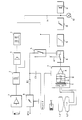
- a goods provided with a resonance label E are either brought to the cash register or are collected from a packing table after payment at the cash register.
- the resonance label E must be deactivated, which is initiated by actuating a switching element.
- This switching element can simply be manually, e.g. by the cashier to be operated, but is preferably formed by a sensor LDR, which automatically detects the passage of the goods and activates the deactivation circuit.
- the sensor LDR is formed by a light barrier or a light reflector with a photoelectric converter LDR, but various configurations are possible, for example a piezosensor that detects the weight of the goods on a base or a circle that simulates the inspection circuit at the department store exit, the one Sends out resonance vibration and uses the "echo" of the label E to determine its presence.
- An amplifier 1 is connected downstream of the sensor LDR, in particular one with a large gain, such as a threshold switch, which converts the voltage change at the output of the sensor LDR into a voltage step. From this step signal, a timing element 2, in particular a monoflop, is triggered, possibly via a coupling capacitor which supplies a needle pulse, which keeps a downstream OR gate 3 open for a predetermined time.
- a pulse generator 4 is switched on via the OR gate 3 switches, which emits at least two, preferably more, pulses with interposed pulse pauses.
- the pulse pause times are preferably a multiple of the pulse times.
- the pulse sequence delivered in this way serves a dual purpose, namely on the one hand to ensure the destruction of the resonance tag E (if this is not already possible with the first pulse) and on the other hand to check the success of the destruction. Since the lowest possible energy is used, the destruction can fail if the label E is placed on a very large piece of goods at a location distant from the transmitting antenna L1, for example on the underside.
- a voltage converter 6 charges a capacitor C1 via a resistor R1.
- a resistor is referred to here, then it is understood to mean any circuit which results in a current resistor.
- transistors can also be operated as variable resistors.
- the capacitor C1 is connected to ground via a controllable switch 5, the switch 5 being closed by the pulses from the pulse generator 5. It is therefore understood that the pulse pause times are to be dimensioned such that the capacitor C1 can be recharged by the voltage converter 6 during this time.
- the timer 2 operates here to a certain extent as a gate circuit for determining the Number of pulses to be output by the pulse generator 4. It would therefore be readily possible to place a gate circuit at the output of a free-running pulse generator 4 and to pass pulses only during a predetermined time. It would also be conceivable to design the pulse generator 4 as a start-stop generator instead of the timing element 2, said generator generating a predetermined number of pulses after being triggered by the pulse from the amplifier 1.
- the ratio of pulse to pause time can advantageously be of the order of 1: 10000.
- the pulse pause times between the pulses of the pulse generator 4 will be discussed again. Normally, the pause times on such a generator are always the same, and the pulses occur periodically. However, this means that the pulses are emitted at a predetermined frequency. This can be a disadvantage for the present purposes if interference is to be expected from such a frequency. It is therefore expedient to make the pulse pause times uneven by switching the pulse generator 4 accordingly. This can either be done in such a way that they are determined by a connected or integrated random generator, or - as is preferred - that they are changed according to a predetermined law, i.e. either lengthened or shortened after each pulse, the extent of this change remaining constant or can be variable.
- the receiving and test antenna L2 can be arranged together with the transmitting antenna L1.
- the transmitting antenna L1 at the cash register and the test antenna L2 at the packing table can also be provided.
- a procedure can also be adopted, as is known from radar and echo sounder technology, in that one and the same antenna is used by switching once as a transmitting antenna and then again as a receiving antenna.
- this is generally not preferred for the present purposes, as will be explained below.
- the relatively strong discharge pulse of capacitor C1 will generally require limiting measures to protect the receiving circuit.
- the number of turns times the area product should be of the same size, but connected in series with the opposite polarity, so that the voltage induced by the excitation coil L1 is compensated to a first approximation.
- the coil L1 when assembling the antenna coils L1, L2, it would be possible to design the coil L1 as a rectangle, in which the receiving coil L2 (as shown) is installed as a symmetrical "8".
- this limiting circuit contains a limiting transformer T, which is preferably designed as a symmetrical ferrite transformer, in particular a relatively small magnetic cross section. This measure alone leads to a first safe limitation and thus to protection of the downstream receiving circuit, because in addition to any down-transformation, the saturation of the ferrite core (which is relatively small in relation to the signal) constitutes a further limitation of the signal emitted.
- a center tap is provided on the secondary side of the transformer T, which is connected to ground.
- An alternative or additional measure can consist in the arrangement (provided on the output side of the ferrite transformer T) of a diode circuit D with diodes connected in parallel with the anit. Silicon diodes or a low junction capacitance are preferred. It would also be possible to use Schottky diodes, which are correspondingly fast, but they are more expensive than the silicon diodes mentioned.
- the circuit 7 has an amplifier A, which is expediently designed as a, in particular fully symmetrical, push-pull amplifier. This is also a protective measure by which common-mode interference signals, in particular capacitively transmitted to the receiving antenna L2, are effectively suppressed. At the same time, the cross-modulation products that occur in the event of overmodulation are reduced.
- a simple measure to circumvent this difficulty is that a timer 8 is in the receiving circuit, which switch 8 only closes the receiving circuit a predetermined time after the discharge pulse has been emitted via the antenna L1.
- this presupposes that the transmitting and receiving circuit are synchronized with one another, ie that the switch 8 is controlled by the transmitting circuit.
- the control input of the switch 8 connected to the switching element LDR, 1-5 discharging the capacitor C1.
- the control line 13 could be connected directly to the circuit of the capacitor C1 or to the switch 5, but this is generally not preferred for dimensional reasons. It is more favorable to connect the control line to the output of the pulse generator 4 (or one of the equivalent circuits mentioned above).
- the delay time after the discharge pulse is emitted until the switch 8 closes is determined by a timer integrated in the switch 8, for example a monoflop, but the timer or monoflop can also be provided separately in line 13.
- the delay time is at least 2 ⁇ s, but must not be too long. A range of 5 to 50 ⁇ s should be optimal. Subsequently, the switch 8 should not remain open too long in order to exclude interference signals as far as possible. An open time of 10 ⁇ s to a maximum of 60 ⁇ s, preferably a maximum of 50 ⁇ s, is entirely satisfactory.
- the above-mentioned predetermined passes until the closing of the switch 8 , Time. This time is chosen such that the interference vibrations generated in the system by the excitation pulse from the antenna L1 have decayed to such an extent that a signal originating from a label E which has remained undamaged at any rate can be recorded significantly.
- the switch 8 If the switch 8 is closed and the receiving antenna L2 receives a ringing from an undamaged label E, these oscillations are expedient integrated in an integrator 9. This may also be protection against interference frequencies, because the integrator 9 is preferably followed by a threshold switch 10, so that a few interference vibrations are not sufficient to exceed the switching threshold of the threshold switch 10.
- the switch 10 serves as a comparator with a predetermined value, namely its threshold value, which can be set via an adjusting resistor (not shown).
- integrator 9 and threshold switch 10 form the detection circuit for a resonance tag E that has remained capable of vibration.
- the detection circuit can be constructed in any way, as is known from radio and radar technology.
- At the output of this detection circuit there is a corresponding evaluation circuit, which is designed either as a pure display with an acoustic display device 11 and / or a visual display device 12, so that the cashier is made aware, for example, that the deactivation process must be repeated.
- the evaluation circuit can also have a signal line 14 in the manner also shown for automating the new deactivation process, which feeds a signal to the switching element LDR, 1-5, which discharges the capacitor C1, for a new start-up.
- the switching element LDR, 1-5 can be implemented in very different ways, and accordingly the output line 14 can also trigger a new switching operation at different points.
- the output line 14 can also trigger a new switching operation at different points.
- any other energy source of corresponding strength can be used instead of a capacitor C1.
- the described deactivation test with the receiving circuit L2, 7-12 could also be carried out in a conventional manner, in particular if the test is carried out at a different location, e.g. at the packing table, is made as the deactivation.
- the advantages achieved by the invention such as speed, etc., are lost when working with frequencies that are matched as precisely as possible.
- a further modification possibility is given at the receiving antenna L2, which is practically designed in the manner of a compensation variometer and can accordingly take all forms known for this design.
Abstract
Description
Die Erfindung bezieht sich auf ein Verfahren nach dem Oberbegriff des Anspruches 1, sowie auf eine Schaltungsanordnung zur Durchführung des Verfahrens.The invention relates to a method according to the preamble of
In Kaufhäusern werden an den Waren zur Sicherung gegen Diebstahl Resonanzetiketten angebracht, die bei Bezahlung an der Kassa, gegebenenfalls aber auch nach Vorweis der Kassabestätigung erst bei Übernahme der Ware am Packtisch, deaktiviert werden müssen. Wird eine Etikette nicht deaktiviert, so lässt sich dies durch eine im Ausgangbereich angeordnete Überwachungsanlage erkennen, die die Etiketten zur Resonanzanregt und an der Resonanz eine nicht deaktiverte Etikette erkennt.In department stores, resonance labels are attached to the goods to protect them against theft, which must be deactivated when paying at the cash desk, but possibly also after showing the cash receipt confirmation when the goods are picked up at the packing table. If a label is not deactivated, this can be recognized by a monitoring system arranged in the exit area, which stimulates the labels to resonate and detects a label that has not been deactivated on the resonance.
Das Deaktivierten erfolgt herkömmlich durch Erregung der Etikette mit etwa der zehnfachen Leistung, was zum Durchbrennen des Schwingkreises bzw. von dessen Kondensator führt. Der hohe Stromstoss kann allerdings auch zur Auslösung eines Alarmes am Ausgang des Warenhauses führen, insbesondere, wenn die Kasse nahe genug angeordnet ist. Die Beseitigung dieser Gefahr ist nur durch teure Schaltungsmassnahmen möglich. Eine weitere Schwierigkeit besteht darin, dass derartig hohe Leistungen eines Senders (und um einen solchen handelt es sich ja hier) der postbehördlichen Genehmigung bedarf und diese nur schwer (oder gar nicht) zu erlangen ist. Um Störalarme auszuschalten ist freilich eine Synchronisation der Überwachungseinrichtung mit der Kassa in der Form möglich, dass die Überwachung in dem Augenblick unterbrochen wird, in dem die Kassa jeweils einen Deaktivierungsstromstoss aussendet. Besonders bei mehreren Kassen bedeutet dies aber, dass die Überwachungseinrichtung letztlich mehr aus- als eingeschaltet ist, so dass unter Umständen ein Dieb mit gestohlener Ware dennoch durchschlüpfen kann.The deactivation takes place conventionally by excitation of the label with about ten times the power, which leads to the burning of the resonant circuit or its capacitor. However, the high current surge can also trigger an alarm at the exit of the department store, especially if the cash register is located close enough. This risk can only be eliminated by expensive circuitry measures. Another difficulty is that such a high performance of a broadcaster (and this is what it is here for) requires the approval of the postal authority and it is difficult (or not at all) to obtain it. In order to switch off false alarms, it is of course possible to synchronize the monitoring device with the cash register in such a way that the monitoring is interrupted at the moment in which the cash register sends out a deactivation current surge. However, particularly in the case of several cash registers, this means that the monitoring device is ultimately switched off more than switched on, so that under certain circumstances a thief with stolen goods can still slip through.
Der Erfindung liegt die Aufgabe zugrunde, ein Verfahren der eingangs genannten Art sowie eine zugehörige Schaltungsanordnung so auszubilden, dass eine Überprüfung der Resonanzetiketten bzw. eine Deaktivierung störungsfrei möglich wird.The invention is based on the object of designing a method of the type mentioned at the outset and an associated circuit arrangement in such a way that the resonance labels can be checked or deactivated without interference.
Ein erster Schritt zur Lösung dieser Aufgabe besteht in der Erkenntnis, dass es der Abgabe der Resonanzfrequenz zur Deaktivierung der Etikette gar nicht bedarf, sondern dass bei entsprechender Stärke ein einzelner Knackimpuls genügt, um den Schwingkreis der Etikette zur Selbstzerstörung anzuregen. Im postalischen Sprachgebrauch ist der Begriff "Knackstörung" in einer Telephonleitung üblich; ein einzelner Impuls aus einem solchen Störsignal ist demnach ein Knackimpuls.A first step towards solving this task is the realization that the resonance frequency does not need to be released to deactivate the label, but that, with the appropriate strength, a single click pulse is sufficient to excite the resonant circuit of the label to self-destruct. In postal parlance, the term "cracking disorder" is common in a telephone line; a single pulse from such an interference signal is therefore a click pulse.
Ausgehend von dieser Erkenntnis besteht die Lösung der gestellten Aufgabe im wesentlichen in den Merkmalen des Kennzeichens des Anspruches 1.Based on this knowledge, the solution to the problem essentially consists in the features of the characterizing part of
Um nun sicher zu gehen, dass die jeweilige Reonanzetikette deaktiviert wird, kann gemäss Anspruch 3 vorgegangen werden, wobei die Etikette dann wohl durch einen weiteren Impuls deaktiviert wird, wenn dies beim ersten Impuls nicht gleich der Fall sein sollte. Es kann aber auch nach Anspruch 4 vorgegangen werden, wobei es bevorzugt ist, beide Vorgangsweisen miteinander zu verbinden, indem mindest ein zweiter Entladungsimpuls abgegeben wird, den dann auch zur Überprüfung dienen mag.In order to be sure that the respective resonance label is deactivated, the procedure according to
Eine Schaltungsanordnung zur Durchführung des erfindungsgemässen Verfahrens ist durch die Merkmale des Anspruches 5 gekennzeichnet.A circuit arrangement for carrying out the method according to the invention is characterized by the features of
In jeder Ausführung der Erfindung werden mehrere Vorteile erhalten:
- Da nur ein einzelner Impuls benötigt wird, sinkt der Energiebedarf, so dass es möglich wird, zum Deaktivieren ein batteriebetriebenes Handgerät zu verwenden, was die Handhabung erleichtert und die Einsatzmöglichkeiten vergrössert;
- da die Überwachungseinrichtung auf eine Impulsserie abgestimmt sind, kann ein einzelner Impuls nicht mehr stören;
- damit fällt die bisher nötige Synchronisation zwischen Deaktivierungsgerät an der Kassa oder am Packtisch einerseits und Überwachungseinrichtung weg, und die Schaltungsanordnung wird vereinfacht;
- überdies fallen auch die postbehördlichen Beschränkungen weg, d.h. eine Bewilligung ist nicht mehr erforderlich;
- auch die Umwelt bzw. in der Umgebung angeordnete Empfangsgeräte sind keiner Störstrahlung mehr ausgesetzt;
- das System wird sicherer, denn VAriationen der Güte des Schwingkreises der Etikette beeinflussen die zu seiner Zerstörung erforderliche Energie weniger, als dies bisher der Fall bei Abgabe eines Schwingungszuges war;
- schliesslich ist die Schaltungsanordnung zum Deaktivieren auch einfacher, da sie keine Abgleichelemente zu enthalten braucht;
zusätzlich erfolgt die Deaktivierung schneller als bisher.Several advantages are obtained in each embodiment of the invention:
- Since only a single pulse is required, the energy requirement drops, so that it is possible to use a battery-operated handheld device for deactivation, which simplifies handling and increases the possible uses;
- Since the monitoring device is matched to a pulse series, a single pulse can no longer interfere;
- This eliminates the previously required synchronization between the deactivation device at the cash register or on the packing table on the one hand and the monitoring device, and the circuit arrangement is simplified;
- In addition, the postal authority restrictions no longer apply, meaning that a permit is no longer required;
- The environment or the receivers arranged in the vicinity are no longer exposed to interference;
the system becomes more secure, because variations in the quality of the oscillating circuit of the label influence the energy required to destroy it less than was previously the case when a vibration train was emitted;
- Finally, the circuit arrangement for deactivation is also simpler since it does not need to contain any adjustment elements;
in addition, deactivation is faster than before.
Weitere Einzelheiten der Erfindung ergeben sich an Hand der nachfolgenden Beschreibung eines in der Zeichnung schematisch dargestellten Ausführungsbeispieles.Further details of the invention will become apparent from the following description of an embodiment shown schematically in the drawing.
Es sei angenommen, dass eine mit einer Resonanzetikette E versehene Ware entweder zur Kassa gebracht oder nach Bezahlung bei der Kassa von einem Packtisch abgeholt wird.It is assumed that a goods provided with a resonance label E are either brought to the cash register or are collected from a packing table after payment at the cash register.
In jedem Falle muss nach der Bezahlung der Ware die Resonanzetikette E deaktiviert werden, was durch Betätigung eines Schaltelementes eingeleitet wird. Dieses Schaltelement kann einfach ein von Hand, z.B. von der Kassierin, zu betätigender Schalter sein, wird aber bevorzugt von einem Sensor LDR gebildet, der automatisch das Vorüberkommen der Ware feststellt und den Deaktivierungskreis in Tätigkeit setzt. Im dargestellten Ausführungsbeispiel ist der Sensor LDR von einer Lichtschranke oder einem Lichtreflektor mit einem lichtelektrischen Wandler LDR gebildet, doch sind verschiedene Ausgestaltungen möglich, beispielsweise ein Piezogeber, der das Gewicht der Ware an einer Unterlage feststellt oder ein dem Überprüfungskreis am Warenhausausgang nachgebildeter Kreis, der eine Resonanzschwingung aussendet und an Hand des "Echos" von der Etikette E deren Vorhandensein feststellt.In any case, after the goods have been paid for, the resonance label E must be deactivated, which is initiated by actuating a switching element. This switching element can simply be manually, e.g. by the cashier to be operated, but is preferably formed by a sensor LDR, which automatically detects the passage of the goods and activates the deactivation circuit. In the exemplary embodiment shown, the sensor LDR is formed by a light barrier or a light reflector with a photoelectric converter LDR, but various configurations are possible, for example a piezosensor that detects the weight of the goods on a base or a circle that simulates the inspection circuit at the department store exit, the one Sends out resonance vibration and uses the "echo" of the label E to determine its presence.
Dem Sensor LDR ist ein Verstärker 1 nachgeschaltet, insbesondere einer mit grosser Verstärkung, wie ein Schwellwertschalter, der die Spannungsänderung am Ausgange des Sensors LDR in einen Spannungssprung umsetzt. Von diesem Sprungsignal wird, gegebenenfalls über einen einen Nadelimpuls liefernden Koppelkondensator, ein Zeitglied 2, insbesondere ein Monoflop, angestossen, das ein nachgeschaltetes ODER-Glied 3 für eine vorbestimmte Zeit offen hält.An
Wenn hier von einem einen Nadelimpuls liefernden Koppelkondensator die Rede ist, so sei hier angemerkt, dass es bereits dieser sein könnte, der den Entladungsimpuls an Stelle des später beschriebenen Kondensators C1 an eine Sendeantenne L1 liefert, doch sei nachstehend eine günstigere Ausführung an Hand der Darstellung und der Funktion der gezeigten Stufen 3 und 4 beschrieben.If a coupling capacitor delivering a needle pulse is mentioned here, it should be noted here that it could already be the one that delivers the discharge pulse instead of the capacitor C1 described later to a transmitting antenna L1, but below is a more favorable embodiment based on the illustration and the function of
Über das ODER-Gatter 3 wird ein Impulsgenerator 4 einge schaltet, der zumindest zwei, vorzugsweise mehr, Impulse mit dazwischenliegenden Impulspausen abgibt. Die Impulspausenzeiten betragen vorzugsweise ein Vielfaches der Impulszeiten. Wie später noch beschrieben wird, dient die so abgegebene Impulsfolge eine doppelten Zweck, nämlich einerseits der Sicherung der Zerstörung der Resonanzetikette E (falls dies nicht schon beim ersten Impuls gelingt), anderseits zur Überprüfung des Zerstörungserfolges. Da nämlich mit möglichst geringer Energie gearbeitet wird, kanna der Zerstörungserfolg dann ausbleiben, wenn die Etikette E etwa an einem sehr grossen Warenstück an einem von der Sendeantenne L1 entfernten Ort, z.B. an der Unterseite angeordnet ist. Stellt sich in so einem Falle durch den später beschriebenen Prüfkreis heraus, dass der Schwingkreis der Etikette E noch intakt ist (und daher am Ausgang des Warenhauses fälschlich einen Diebstahlsalarm durch die dort angebrachte Überprüfungseinrichtung auslösen könnte), so braucht die Ware nur umgedreht und die Deaktivierung wiederholt werden.A pulse generator 4 is switched on via the
Ein Spannungsumsetzer 6 lädt über einen Widerstand R1 einen Kondensator C1 auf. Wenn hier von einem Widerstand die Rede ist, so sei darunter jegliche einen STromwiderstand ergebende Schaltung verstanden. Es ist beispielsweise bekannt, dass etwa auch Transistoren als variable Widerstände betrieben werden können. Der Kondensator C1 liegt über einem steuerbaren Schalter 5 an Masse, wobei der Schalter 5 jeweils durch die Impulse aus dem Impulsgenerator 5 geschlossen wird. Es versteht sich daher, dass die Impulspausenzeiten so zu bemessen sind, dass in dieser Zeit der Kondensator C1 durch den Spannungsumsetzer 6 wieder aufgeladen werden kann.A voltage converter 6 charges a capacitor C1 via a resistor R1. If a resistor is referred to here, then it is understood to mean any circuit which results in a current resistor. For example, it is known that transistors can also be operated as variable resistors. The capacitor C1 is connected to ground via a
Aus der bisherigen Beschreibung lässt sich eine weitere Abwandlungsmöglichkeit erkennen: Das Zeitglied 2 arbeitet hier gewissermassen als Torschaltung zur Festlegung der Anzahl der vom Impulsgenerator 4 abzugebenden Impulse. Es wäre also ohne weiteres möglich, eine Torschaltung an den Ausgang eines frei laufenden Impulsgenerators 4 zu legen und nur während einer vorbestimmten Zeit Impulse durchzulassen. Ebenso wäre es denkbar, an Stelle des Zeitgliedes 2 den Impulsgenerator 4 als Start-Stop-Generator auszubilden, der nach dem Anstossen durch den Impuls vom Verstärker 1 eine vorbestimmte Anzahl von Impulsen abgibt. Das Verhältnis von Impuls- zu Pausenzeit kann vorteilhaft in der Grössenordnung von 1:10000 liegen.Another modification can be seen from the description so far: the
Hier sei nochmals auf die Impulspausenzeiten zwischen den Impulsen des Impulsgenerators 4 eingegangen. Normalerweise sind an einem solchen Generator die Pausenzeiten stets gleich gross, und die Impulse erfolgen periodisch. Dies bedeutet aber, dass die Impulse mit einer vorbestimmten Frequenz abgegeben werden. Dies kann für die vorliegenden Zwecke einen Nachteil bedeuten, wenn durch eine solche Frequenz Störungen zu erwarten sind. Deshalb ist es zweckmässig, die Impulspausenzeiten durch entsprechende Schaltung des Impulsgenerators 4 ungleichmässig zu machen. Dies kann entweder so erfolgen, dass sie von einem angeschlossenen oder integrierten Zufallsgenerator bestimmt werden, oder - wie dies bevorzugt ist - dass sie nach einer vorbestimmten Gesetzmässigkeit verändert, also entweder nach jedem Impuls verlängert oder verkürzt werden, wobei das Mass dieser Veränderung wieder gleichbleibend oder variabel sein kann.Here, the pulse pause times between the pulses of the pulse generator 4 will be discussed again. Normally, the pause times on such a generator are always the same, and the pulses occur periodically. However, this means that the pulses are emitted at a predetermined frequency. This can be a disadvantage for the present purposes if interference is to be expected from such a frequency. It is therefore expedient to make the pulse pause times uneven by switching the pulse generator 4 accordingly. This can either be done in such a way that they are determined by a connected or integrated random generator, or - as is preferred - that they are changed according to a predetermined law, i.e. either lengthened or shortened after each pulse, the extent of this change remaining constant or can be variable.
Immerdann, wenn über einen vom Impulsgenerator 4 ausgesandten Impuls der Schalter 5 geschlossen wird, entlädt sich der Kondensator C1, und dieser Entladungsimpuls (= Knackimpuls) wird auf die Senderspule L1 übertragen. Der so ausgesandte Impuls reicht - wie gefunden wurde - aus, die Resonanzetikette E zu zerstören, denn sie wird durch diesen Impuls jeweils zu Eigenschwingungen angeregt, die dann exponentiell abklingen, wenn nicht vorher die Zerstörung er folgt. Die Zerstörung erfolgt dabei in üblicherweise, meist am Kondensator des Etikettenschwingkreises.Whenever the
Erfolgt hingegen keine Zerstörung und klingt die Schwingungserregung der Etikette E nach Erhalt eines Entladungsimpulses aus der Senderantenne L1 ab, so kann dies vorzugsweise mit Hilfe eines Prüfkreises festgestellt werden, der eine Empfangsantenne L2 zur Aufnahme der Erregungsschwingung der Etikette E aufweist.If, on the other hand, there is no destruction and the vibration excitation of the label E decays after receiving a discharge pulse from the transmitter antenna L1, this can preferably be determined with the aid of a test circuit which has a receiving antenna L2 for recording the excitation vibration of the label E.
Hier sei noch eine Bemerkung zur Ausbildung des Kondensators C1 eingefügt. Dieser muss jedenfalls so bemessen sein, dass einerseits die Etikette E mit grosser Sicherheit schon beim ersten Entladungsimpuls zerstört wird, so dass die später abgegebenen Impulse möglichst nur zur Durchführung der Prüfung dienen. Anderseits soll er klein genug sein, damit der Entladungsimpuls nicht einen zu grossen Energieinhalt besitzt und Störungen hervorrufen könnte. Es wurde nun gefunden, dass eine Grösse von maximal 60 nF, vorzugsweise maximal 50 nF durchaus ausreichend ist, und dass ein praktisch zweckmässiger Bereich 5 bis 50 nF umfasst. Beispielsweise ist eine Bemassung von 10 nF ± 5 nF durchaus realistisch.A comment regarding the formation of the capacitor C1 is inserted here. In any case, this must be dimensioned such that, on the one hand, the label E is almost certainly destroyed during the first discharge pulse, so that the pulses subsequently emitted serve only to carry out the test if possible. On the other hand, it should be small enough so that the discharge pulse does not have too much energy and could cause interference. It has now been found that a size of at most 60 nF, preferably at most 50 nF, is quite sufficient and that a practically expedient range comprises 5 to 50 nF. For example, a dimension of 10 nF ± 5 nF is quite realistic.
Die Empfangs- und Prüfantenne L2 kann zusammen mit der Sendeantenne L1 angeordnet sein. Es kann aber auch die Sendeantenne L1 an der Kassa, die Prüfantenne L2 am Packtisch vorgesehen werden. Theoretisch kann auch eine Vorgangsweise eingeschlagen werden, wie sie aus der Radar- und Echolot-Technik bekannt ist, indem ein und dieselbe Antenne durch Umschalten einmal als Sende- dann wieder als Empfangsantenne verwendet wird. Dies ist aber für die vorliegenden Zwecke im allgemeinen nicht bevorzugt, wie nachstehend erläutert wird.The receiving and test antenna L2 can be arranged together with the transmitting antenna L1. However, the transmitting antenna L1 at the cash register and the test antenna L2 at the packing table can also be provided. Theoretically, a procedure can also be adopted, as is known from radar and echo sounder technology, in that one and the same antenna is used by switching once as a transmitting antenna and then again as a receiving antenna. However, this is generally not preferred for the present purposes, as will be explained below.
Der relativ starke Entladungsimpuls des Kondensators C1 wird nämlich im allgemeinen Begrenzungsmassnahmen zum Schutze der Empfangsschaltung erforderlich machen. Wie in der Zeichnung angedeutet ist, ist es vorteilhaft, mindestens zwei Gruppen von, insbesondere flächigen, Teilspulen L2ʹ,L2ʺ für die Antenne L2 vorzusehen. Die Windungszahl mal Flächenprodukt sollte dabei gleich gross, aber mit entgegengesetzter Polarität in Reihe geschaltet sein, so dass sich die aus der Anregungsspule L1 induzierte Spannung in erster Näherung kompensiert. Beipielsweise wäre es beim Zusammenbau der Antennenspulen L1, L2 möglich, die Spule L1 als Rechteck zu gestalten, in dem die Empfangsspule L2 (in der gezeigten Weise) als symmetrische "8" eingebaut ist. Damit ergibt sich am Kreuzungspunkt der beiden Teilspulen L2ʹ und L2ʺ nahezu ein Signal von Null, wogegen das Signal an den Aussenseiten dieser Teilspulen am grössten ist. Dort wird gemäss dem gezeigten Ausführungsbeispiel auch das Signal an der Teilspule L2ʺ abgenommen.The relatively strong discharge pulse of capacitor C1 will generally require limiting measures to protect the receiving circuit. As indicated in the drawing, it is advantageous to provide at least two groups of, in particular planar, partial coils L2ʹ, L2ʺ for the antenna L2. The number of turns times the area product should be of the same size, but connected in series with the opposite polarity, so that the voltage induced by the excitation coil L1 is compensated to a first approximation. For example, when assembling the antenna coils L1, L2, it would be possible to design the coil L1 as a rectangle, in which the receiving coil L2 (as shown) is installed as a symmetrical "8". This results in a signal of almost zero at the intersection of the two coil sections L2ʹ and L2ʺ, whereas the signal on the outside of these coil sections is greatest. There, according to the exemplary embodiment shown, the signal at the sub-coil L2ʺ is also taken.
Das an der Teilspule L2ʺ abgenommene Signal wird nun zweckmässig einer Begrenzungsschaltung (Kreis 7) zugeführt, bevor sie dem eigentlichen Empfangskreis zugeleitet wird. Diese Begrenzungsschaltung enthält eingangsseitig einen Begrenzungstransformator T, der vorzugsweise als symmetrischer Ferritübertrager, insbesondere relativ kleinen magnetischen Querschnitts, ausgebildet ist. Schon diese Massnahme führt zu einer ersten sicheren Begrenzung und damit zu einem Schutz der nachgeordneten Empfangsschaltung, denn zusätzlich zu einer allfälligen Heruntertransformation stellt die Sättigung des mit (relativ zum Signal) geringen magnetischen Querschnitt ausgebildeten Ferritkernes eine weitere Begrenzung des abgegebenen Signales dar.The signal picked up at the sub-coil L2 wird is now expediently fed to a limiting circuit (circuit 7) before it is fed to the actual receiving circuit. On the input side, this limiting circuit contains a limiting transformer T, which is preferably designed as a symmetrical ferrite transformer, in particular a relatively small magnetic cross section. This measure alone leads to a first safe limitation and thus to protection of the downstream receiving circuit, because in addition to any down-transformation, the saturation of the ferrite core (which is relatively small in relation to the signal) constitutes a further limitation of the signal emitted.
An der Sekundärseite des Transformators T ist eine Mittelanzapfung vorgesehen, die an Masse liegt.A center tap is provided on the secondary side of the transformer T, which is connected to ground.
Eine alternative oder zusätzliche Massnahme kann in der (ausgangsseitig des Ferritübertragers T vorgesehenen) Anordnung einer Diodenschaltung D mit anitparallel geschalteten Dioden bestehen. Bevorzugt sind siliziumdioden bzw. eine geringe Sperrschichtkapazität. Auch die Verwendung von Schottky-Dioden wäre möglich, die entsprechend schnell sind, doch sind diese teurer als die erwähnten Siliziumdioden.An alternative or additional measure can consist in the arrangement (provided on the output side of the ferrite transformer T) of a diode circuit D with diodes connected in parallel with the anit. Silicon diodes or a low junction capacitance are preferred. It would also be possible to use Schottky diodes, which are correspondingly fast, but they are more expensive than the silicon diodes mentioned.
Dazwischen besitzt der Kreis 7 einen Verstärker A, der zweckmässig als, insbesondere voll symmetrischer, Gegentaktverstärker ausgebildet ist. Auch dies ist eine Schutzmassnahme, durch die gleichtaktige, insbesondere kapazitiv auf die Empfangsantenne L2 übertragene, Störsignale wirkungsvoll unterdrückt werden. Gleichzeitig werden die bei Übersteuerung auftretenden Kreuzmodulationsprodukte verringert.In between, the
Es hat nun nicht nur keinen Sinn, sondern ist auch eher nachteilig, wenn der Empfangsschaltung auch das Knacksignal des Entladungsimpulses vom Kondensator C1 zugeführt würde. Der Empfangskreis würde einerseits stark belastet und müsste durch zusätzliche Sicherungsmassnahmen verteuert werden, anderseits soll ja nicht der Entladungsimpuls selbst, sondern ein etwaiges Nachschwingen des Schwingkreises der Etikette E überprüft werden, falls diese unzerstört bleibt.It not only makes no sense, but is also rather disadvantageous if the cracking signal of the discharge pulse from the capacitor C1 were also supplied to the receiving circuit. The receiving circuit would be heavily burdened on the one hand and would have to be made more expensive by additional security measures, on the other hand it should not be the discharge pulse itself that is to be checked, but a possible reverberation of the oscillating circuit of the label E if it remains undamaged.
Eine einfache Massnahme zur Umgehund dieser Schwierigkeit liegt darin, dass ein Zeitschalter 8 im Empfangskreis liegt, welcher Schalter 8 den Empfangskreis erst eine vorbestimmte Zeit nach Abgabe des Entladungsimpulses über die Antenne L1 schliesst. Dies setzt natürlich voraus, dass Sende- und Empfangskreis miteinander synchronisiert sind, d.h. dass der Schalter 8 vom Sendekreis gesteuert wird. Zu diesem Zwecke ist der Steuereingang des Schalters 8 mit dem den Kondensator C1 entladenden Schaltglied LDR, 1-5 verbunden. Im Prinzip könnte die Steuerleitung 13 mit dem Stromkreis des Kondesnators C1 bzw. mit dem Schalter 5 unmittelbar verbunden sein, doch wird dies aus Dimensionsgründen im allgemeinen nicht bevorzugt. Günstiger ist es, die Steuerleitung an den Ausgang des Impulsgenerators 4 (oder einer der oben erwähnten Ersatzschaltungen) zu legen. Die Verzögerungszeit nach der Abgabe des Entladungsimpulses bis zum Schliessen des Schalters 8 wird durch ein in den Schalter 8 integriertes Zeitglied, z.B. ein Monoflop, bestimmt, doch kann das Zeitglied bzw. Monoflop auch gesondert in der Leitung 13 vorgesehen sein. Die Verzögerungszeit beträgt mindestens 2 µs, darf aber auch nicht zu lange sein. Ein Bereich von 5 bis 50 µs dürfte optimal sein. Anschliessend soll der Schalter 8 aber auch nicht zu lange offen bleiben, um Störsignale möglichst auszuschliessen. Eine Offenzeit von 10 µs bis maximal 60 µs, vorzugsweise maximal 50 µs, ist durchaus zufriedenstellend.A simple measure to circumvent this difficulty is that a
Sobald also der Entladungsimpuls vom Kondensator C1 an die Antenne L1 abgegebenen wurde (statt des Kondensators C1 könnte an sich jede beliebige Energiequelle entsprechender Stärke vorgesehen sein), vergeht bis zum Schliessen des Schlaters 8 die oben erwähnte, vorbestimmte, gegebenenfalls durch eine nicht dargestellte Jusitereinrichtung einstellbare, Zeit. Diese Zeit wird so gewählt, dass die durch den Anregungsimpuls von der Antenne L1 im System erzeugten Störschwingungen soweit abgeklungen sind, dass ein von einer allenfalls unzerstört gebliebenen Etikette E stammendes Signal signifikant aufgenommen werden kann.As soon as the discharge pulse from the capacitor C1 has been delivered to the antenna L1 (instead of the capacitor C1, any energy source of appropriate strength could be provided), the above-mentioned predetermined, possibly adjustable by a jusiter device, not shown, passes until the closing of the
Ist der Schalter 8 geschlossen und erhält die Empfangsantenne L2 eine Nachschwingung von einer unzerstört gebliebenen Etikette E, so werden diese Schwingungen zweckmässig in einem Integrator 9 aufintegriert. Auch dies mag ein Schutz vor Störfrequenzen sein, denn dem Integrator 9 ist bevorzugt ein Schwellwertschalter 10 nachgeschaltet, so dass wenige Störschwingungen nicht ausreichen, um die Schaltschwelle des Schwellwertschalters 10 zu überschreiten. Praktisch dient der Schalter 10 als Komparator mit einem vorgegebenen Wert, nämlich seinem, allenfalls über einen nicht dargestellten Justierwiderstand einstellbaren, Schwellwert.If the
Integrator 9 und Schwellwertschalter 10 bilden in der Praxis die Erkennungsschaltung für eine schwingungsfähig gebliebene Resonanzetikette E. Gewünschtenfalls kann die Erkennungsschaltung in beliebiger Weise aufgebaut sein, wie dies aus der Radio- und der Radartechnik bekannt ist. Am Ausgang dieser Erkennungsschaltung liegt dann eine entsprechende Auswerteschaltung, die entweder als reine Anzeige mit einer akustischen Anzeigeeinrichtung 11 und/oder einer visuellen Anzeigeeinrichtung 12 ausgebildet ist, so dass etwa die Kassierin darauf aufmerksam gemacht wird, dass der Deaktivierungsvorgang wiederholt werden muss. Die Auswerteschaltung kann aber auch in der ebenfalls gezeigten Weise zur Automatisierung des neuerlichen Deaktivierungsvorganges eine Signalleitung 14 besitzen, die direkt dem den Kondensator C1 entladenden Schaltglied LDR, 1-5 ein Signal zur neuerlichen Einschaltung zuführt.In practice,
Es wurde schon erwähnt, dass das Schaltglied LDR, 1-5 auf sehr verschiedene Arten verwirklicht sein kann, und dementsprechend kann auch die Ausgangsleitung 14 an verschiedenen Punkten einen neuerlichen Schaltvorgang auslösen. Beispielsweise wäre es denkbar, die Leitung 14 an den Eingang des Zeitgliedes 2 zu legen, so dass dieses wahlweise vom Sensor LDR oder über die Leitung 14 eingeschaltet wird. Einfacher ist es jedoch, das schon erwähnte ODER-Glied 3 vorzusehen und die Leitung 14 an dessen zweiten Eingang zu legen, so dass der Impulsgenerator 4 für die Dauer eines über die Leitung 14 geführten Signales Impulse (d.h. mindestens einen) abgibt, um die noch unzerstörte Etikette E endgültig zu deaktivieren. Auf diese Weise können Fehlalarme besser vermieden werden.It has already been mentioned that the switching element LDR, 1-5 can be implemented in very different ways, and accordingly the
Es wurde bereits erwähnt, dass an Stelle eines Kondensators C1 im Prinzip jede andere Energiequelle entsprechender Stärke eingesetzt werden kann. In letzterem Falle werden sich im allgemeinen keine Nadelimpulse ergeben, und es mag sogar sein, dass dann Impulsformerstufen nötig sind. Die geschilderte Deaktivierungsprüfung mit der Empfangsschaltung L2, 7-12 könnte auch in herkömmlicher Weise vorgenommen werden, insbesondere wenn die Prüfung an einem anderen Ort, z.B. am Packtisch, vorgenommen wird, als die Deaktivierung. Allerdings gehen dann die durch die Erfindung erzielten Vorteile, wie die Schnelligkeit usw. verloren, wenn mit möglichst genau abgestimmten Frequenzen gearbeitet wird.It has already been mentioned that, in principle, any other energy source of corresponding strength can be used instead of a capacitor C1. In the latter case, there will generally be no needle pulses, and it may even be that pulse shaping stages are then necessary. The described deactivation test with the receiving circuit L2, 7-12 could also be carried out in a conventional manner, in particular if the test is carried out at a different location, e.g. at the packing table, is made as the deactivation. However, the advantages achieved by the invention, such as speed, etc., are lost when working with frequencies that are matched as precisely as possible.
Im Rahmen der Erfindung sind zahlreiche Modifikationen denkbar; beispielsweise könnten an Stelle eines Kondensators C1 auch deren mehrere vorgesehen sein, die entweder zueinander parallel geschaltet sind, vorzugsweise hingegen nacheinander zur Abgabe je eines Entladungsimpulses eingeschaltet werden. Dabei kann es zur Sicherung der Deaktivierung der Etikette günstig sein, wenn die nacheinander eingeschalteten und so entladenen Kondensatoren steigende Grösse aufweisen. Es versteht sich auch, dass der Spannungsumsetzer 6 an sich nicht unbedingt erforderlich ist, jedoch durch Erhöhung der Aufladespannung die Aufladezeit erheblich herabzusetzen vermag, wodurch die Vorgänge noch rascher vor sich gehen können.Numerous modifications are conceivable within the scope of the invention; For example, instead of one capacitor C1, there could also be several, which are either connected in parallel to one another, but are preferably switched on one after the other in order to emit one discharge pulse each. In order to ensure the deactivation of the label, it can be advantageous if the capacitors which are switched on one after the other and are thus discharged have increasing sizes. It is also understood that the
Eine weitere Abwandlungsmöglichkeit ist an der Empfangsantenne L2 gegeben, die praktisch nach Art eines Kompensationsvariometers ausgebildet ist und dementsprechend alle für diese Ausbildung bekannten Formen annehmen kann.A further modification possibility is given at the receiving antenna L2, which is practically designed in the manner of a compensation variometer and can accordingly take all forms known for this design.
Claims (10)
und dass vorzugsweise die Impulspausen zwischen den Entladungsimpulsen ungleichmässig lang sind, beispielsweise mit einer Zufallsverteilung, insbesondere aber mit einer gesetzmässigen Veränderung.3. The method according to claim 1 or 2, characterized in that at least two, preferably more, individual discharge pulses are emitted with pulse pauses in between,
and that preferably the pulse pauses between the discharge pulses are unevenly long, for example with a random distribution, but in particular with a regular change.
und dass bevorzugt die Empfangsschaltung erst nach einer vorbestimmten Zeitspanne nach Abgabe des deaktivierenden Entladungsimpulses eingeschaltet wird, wobei die vorbestimmte Zeit insbesondere zumindest 2 us, zweckmässig 5 us bis 30 us, beträgt, und dass gege benenfalls die Offenzeit, in der die Empfangsschaltung eingeschaltet ist, 10 us bis 60 us, bevorzugt maximal 50 us, dauert.4. The method according to any one of the preceding claims, characterized in that after the discharge pulse is emitted at least one excitation signal for the resonance label (E) for checking that the deactivation has taken place, preferably in the form of at least one further discharge pulse, a possible resonance signal of the label (E ) is received via a receiving circuit,
and that the receiving circuit is preferably switched on only after a predetermined period of time after the deactivating discharge pulse has been emitted, the predetermined time being in particular at least 2 us, suitably 5 us to 30 us, and that against The open time, in which the receiving circuit is switched on, lasts 10 us to 60 us, preferably a maximum of 50 us.
Priority Applications (1)
| Application Number | Priority Date | Filing Date | Title |
|---|---|---|---|
| AT88105582T ATE86403T1 (en) | 1987-04-23 | 1988-04-08 | METHOD OF DEACTIVATING A RESONANCE TAG AND CIRCUIT ARRANGEMENT FOR CARRYING OUT THE METHOD. |
Applications Claiming Priority (2)
| Application Number | Priority Date | Filing Date | Title |
|---|---|---|---|
| CH156487 | 1987-04-23 | ||
| CH1564/87 | 1987-04-23 |
Publications (2)
| Publication Number | Publication Date |
|---|---|
| EP0287905A1 true EP0287905A1 (en) | 1988-10-26 |
| EP0287905B1 EP0287905B1 (en) | 1993-03-03 |
Family
ID=4213376
Family Applications (1)
| Application Number | Title | Priority Date | Filing Date |
|---|---|---|---|
| EP88105582A Expired - Lifetime EP0287905B1 (en) | 1987-04-23 | 1988-04-08 | Method for deactivating a resonant target, and circuit for carrying out this method |
Country Status (6)
| Country | Link |
|---|---|
| US (1) | US4906974A (en) |
| EP (1) | EP0287905B1 (en) |
| JP (1) | JP2575173B2 (en) |
| AT (1) | ATE86403T1 (en) |
| DE (1) | DE3878717D1 (en) |
| ES (1) | ES2039005T3 (en) |
Cited By (12)
| Publication number | Priority date | Publication date | Assignee | Title |
|---|---|---|---|---|
| US5027106A (en) * | 1989-12-27 | 1991-06-25 | Checkpoint Systems, Inc. | Method and apparatus for electronic article surveillance |
| WO1991009387A1 (en) * | 1989-12-20 | 1991-06-27 | Actron Entwicklungs Ag | Deactivatable resonance label |
| EP0439237A1 (en) * | 1990-01-25 | 1991-07-31 | N.V. Nederlandsche Apparatenfabriek NEDAP | Method and apparatus for deactivating electromagnetic detection labels |
| EP0454021A1 (en) * | 1990-04-25 | 1991-10-30 | Actron Entwicklungs AG | Method for deactivating a resonant tag and circuit for carrying out this method |
| EP0478092A1 (en) * | 1990-09-28 | 1992-04-01 | N.V. Nederlandsche Apparatenfabriek NEDAP | Deactivating device |
| FR2669756A1 (en) * | 1990-11-23 | 1992-05-29 | Cga Hbs | System for recording and invalidating the identification of a product |
| EP0499582A1 (en) * | 1991-02-12 | 1992-08-19 | Actron Entwicklungs AG | Deactivating device for resonance tags |
| WO1993010514A1 (en) * | 1991-11-14 | 1993-05-27 | Joergensen Poul Richter | Method of activation and deactivation of tags and apparatus for activating and deactivating said tags |
| US5257010A (en) * | 1990-04-25 | 1993-10-26 | Actron Entwicklungs | Process for the deactivation of a reasonance label and circuit arrangement for the execution of the process |
| NL1002150C2 (en) * | 1996-01-23 | 1997-07-25 | Nedap Nv | Deactivation system with improved reliability. |
| WO2002005238A2 (en) * | 2000-07-07 | 2002-01-17 | 3M Innovative Properties Company | Device for changing the status of dual status magnetic electronic article surveillance markers |
| US6778087B2 (en) | 2001-06-15 | 2004-08-17 | 3M Innovative Properties Company | Dual axis magnetic field EAS device |
Families Citing this family (5)
| Publication number | Priority date | Publication date | Assignee | Title |
|---|---|---|---|---|
| DE4015779A1 (en) * | 1990-05-16 | 1991-11-21 | Minnesota Mining & Mfg | Electro magnetic desensitiser appts. |
| US5805065A (en) * | 1991-05-08 | 1998-09-08 | Minnesota Mining And Manufacturing Company | Electro-magnetic desensitizer |
| NL9202067A (en) * | 1992-11-27 | 1994-06-16 | Dutch A & A Trading Bv | Detection label. |
| ES2152152B1 (en) * | 1998-05-22 | 2001-08-01 | El Corte Ingles S A | CONTROLLER OF SECURITY LABELS USED IN THE COMMERCIALIZATION OF GOODS. |
| GB2500134B (en) * | 2009-12-08 | 2014-02-12 | Redcliffe Magtronics Ltd | Hand-held tag detector |
Citations (2)
| Publication number | Priority date | Publication date | Assignee | Title |
|---|---|---|---|---|
| US3938044A (en) * | 1973-11-14 | 1976-02-10 | Lichtblau G J | Antenna apparatus for an electronic security system |
| WO1985004975A1 (en) * | 1982-05-10 | 1985-11-07 | Arthur D. Little, Inc. | Resonant tag and deactivator for use in an electronic security system |
Family Cites Families (3)
| Publication number | Priority date | Publication date | Assignee | Title |
|---|---|---|---|---|
| US4686516A (en) * | 1984-11-26 | 1987-08-11 | Sensormatic Electronics Corporation | Method, system and apparatus for use in article surveillance |
| US4736207A (en) * | 1986-01-31 | 1988-04-05 | Sensormatic Electronics Corporation | Tag device and method for electronic article surveillance |
| CH677988A5 (en) * | 1986-07-30 | 1991-07-15 | Actron Entwicklungs Ag |
-
1988
- 1988-04-08 DE DE8888105582T patent/DE3878717D1/en not_active Expired - Fee Related
- 1988-04-08 EP EP88105582A patent/EP0287905B1/en not_active Expired - Lifetime
- 1988-04-08 AT AT88105582T patent/ATE86403T1/en not_active IP Right Cessation
- 1988-04-08 ES ES198888105582T patent/ES2039005T3/en not_active Expired - Lifetime
- 1988-04-14 JP JP63090443A patent/JP2575173B2/en not_active Expired - Lifetime
- 1988-04-22 US US07/185,037 patent/US4906974A/en not_active Expired - Lifetime
Patent Citations (2)
| Publication number | Priority date | Publication date | Assignee | Title |
|---|---|---|---|---|
| US3938044A (en) * | 1973-11-14 | 1976-02-10 | Lichtblau G J | Antenna apparatus for an electronic security system |
| WO1985004975A1 (en) * | 1982-05-10 | 1985-11-07 | Arthur D. Little, Inc. | Resonant tag and deactivator for use in an electronic security system |
Cited By (19)
| Publication number | Priority date | Publication date | Assignee | Title |
|---|---|---|---|---|
| WO1991009387A1 (en) * | 1989-12-20 | 1991-06-27 | Actron Entwicklungs Ag | Deactivatable resonance label |
| EP0435538A3 (en) * | 1989-12-27 | 1992-09-23 | Checkpoint Systems, Inc. | Method and apparatus for electronic article surveillance |
| EP0435538A2 (en) * | 1989-12-27 | 1991-07-03 | Checkpoint Systems, Inc. | Method and apparatus for electronic article surveillance |
| US5027106A (en) * | 1989-12-27 | 1991-06-25 | Checkpoint Systems, Inc. | Method and apparatus for electronic article surveillance |
| EP0439237A1 (en) * | 1990-01-25 | 1991-07-31 | N.V. Nederlandsche Apparatenfabriek NEDAP | Method and apparatus for deactivating electromagnetic detection labels |
| EP0454021A1 (en) * | 1990-04-25 | 1991-10-30 | Actron Entwicklungs AG | Method for deactivating a resonant tag and circuit for carrying out this method |
| US5257010A (en) * | 1990-04-25 | 1993-10-26 | Actron Entwicklungs | Process for the deactivation of a reasonance label and circuit arrangement for the execution of the process |
| EP0478092A1 (en) * | 1990-09-28 | 1992-04-01 | N.V. Nederlandsche Apparatenfabriek NEDAP | Deactivating device |
| FR2669756A1 (en) * | 1990-11-23 | 1992-05-29 | Cga Hbs | System for recording and invalidating the identification of a product |
| EP0499582A1 (en) * | 1991-02-12 | 1992-08-19 | Actron Entwicklungs AG | Deactivating device for resonance tags |
| CH682265A5 (en) * | 1991-02-12 | 1993-08-13 | Actron Entwicklungs Ag | |
| WO1993010514A1 (en) * | 1991-11-14 | 1993-05-27 | Joergensen Poul Richter | Method of activation and deactivation of tags and apparatus for activating and deactivating said tags |
| NL1002150C2 (en) * | 1996-01-23 | 1997-07-25 | Nedap Nv | Deactivation system with improved reliability. |
| EP0786749A1 (en) * | 1996-01-23 | 1997-07-30 | N.V. Nederlandsche Apparatenfabriek NEDAP | Deactivation device for electronic theft detection labels with improved reliability |
| WO2002005238A2 (en) * | 2000-07-07 | 2002-01-17 | 3M Innovative Properties Company | Device for changing the status of dual status magnetic electronic article surveillance markers |
| WO2002005238A3 (en) * | 2000-07-07 | 2002-04-11 | 3M Innovative Properties Co | Device for changing the status of dual status magnetic electronic article surveillance markers |
| US6486782B1 (en) | 2000-07-07 | 2002-11-26 | 3M Innovative Properties | Device for changing the status of dual status magnetic electronic article surveillance markers |
| AU2001212106B2 (en) * | 2000-07-07 | 2006-02-16 | 3M Innovative Properties Company | Device for changing the status of dual status magnetic electronic article surveillance markers |
| US6778087B2 (en) | 2001-06-15 | 2004-08-17 | 3M Innovative Properties Company | Dual axis magnetic field EAS device |
Also Published As
| Publication number | Publication date |
|---|---|
| ATE86403T1 (en) | 1993-03-15 |
| DE3878717D1 (en) | 1993-04-08 |
| JPS63282900A (en) | 1988-11-18 |
| US4906974A (en) | 1990-03-06 |
| ES2039005T3 (en) | 1993-08-16 |
| EP0287905B1 (en) | 1993-03-03 |
| JP2575173B2 (en) | 1997-01-22 |
Similar Documents
| Publication | Publication Date | Title |
|---|---|---|
| EP0287905B1 (en) | Method for deactivating a resonant target, and circuit for carrying out this method | |
| DE69738562T2 (en) | MAGNETOMECHANICAL ELECTRONIC GOODS MONITORING SYSTEM WITH PULSED SIGNAL AND TRANSMITTER ANTENNA | |
| DE2605374A1 (en) | METHOD OF ADJUSTING A FIRE AFTER THE FIRING OF A BULLET FROM A FIRE ARM AND DEVICE FOR CARRYING OUT THE PROCEDURE | |
| DE2646160C2 (en) | Method and device for monitoring sound-conducting media | |
| DE2316411A1 (en) | MONITORING SYSTEM AND METHOD USING ELECTROSTATIC AND ELECTROMAGNETIC FIELDS | |
| DE3235434A1 (en) | METHOD AND DEVICE FOR SECURING A SURVEILLANCE ZONE AGAINST THEFT | |
| DE2945183A1 (en) | METHOD FOR DETECTING AN OBJECT INTENDING IN A PROTECTED AREA | |
| DE2815686A1 (en) | DEVICE FOR MONITORING THE POPULATION OF ANIMAL SKULLS, IN PARTICULAR SELECTED SPECIES OF INSECTS | |
| DE2944821A1 (en) | METHOD AND DEVICE FOR TRANSMITTING AND RECEIVING ULTRASOUND, IN PARTICULAR IN DESTRUCTION-FREE TESTING | |
| DE2528544C2 (en) | Device for igniting a pyrotechnic charge | |
| DE2944820A1 (en) | METHOD AND DEVICE FOR TRANSMITTING AND RECEIVING ULTRASOUND | |
| DE2015294A1 (en) | Guiding device | |
| DE1466020B2 (en) | Responder | |
| DE3206285C2 (en) | ||
| DE2651042A1 (en) | IDENTIFICATION SYSTEM | |
| DE2310869A1 (en) | TEST PROCEDURE FOR PLASTIC COATED BOTTLES | |
| DE1295424B (en) | Device for detecting the unauthorized passage of objects at a control point | |
| DE1904836C3 (en) | Transit time measuring device for ultrasonic testing of concrete | |
| DE4414746A1 (en) | Transceiver circuit for an acoustic pulse echo distance measuring system | |
| CH472748A (en) | Device for the wireless identification of objects when passing a spatial barrier | |
| EP0032598B1 (en) | Portable paging receiver with a shift register and a direct current converter | |
| DE2347460A1 (en) | ARMS CONTROL SYSTEM | |
| DE3027283C2 (en) | ||
| DD294678A5 (en) | ARRANGEMENT FOR NON-CONTACT SURVEILLANCE OF A THREAD-MATERIAL MATERIAL | |
| DE2047930B2 (en) | IMPACT DEVICE FOR THE QUALITY CONTROL OF THE BONDING OF ELEMENTS BONDED TOGETHER |
Legal Events
| Date | Code | Title | Description |
|---|---|---|---|
| PUAI | Public reference made under article 153(3) epc to a published international application that has entered the european phase |
Free format text: ORIGINAL CODE: 0009012 |
|
| AK | Designated contracting states |
Kind code of ref document: A1 Designated state(s): AT BE CH DE ES FR GB GR IT LI LU NL SE |
|
| 17P | Request for examination filed |
Effective date: 19890311 |
|
| RAP1 | Party data changed (applicant data changed or rights of an application transferred) |
Owner name: ACTRON ENTWICKLUNGS AG |
|
| 17Q | First examination report despatched |
Effective date: 19910219 |
|
| GRAA | (expected) grant |
Free format text: ORIGINAL CODE: 0009210 |
|
| AK | Designated contracting states |
Kind code of ref document: B1 Designated state(s): AT BE CH DE ES FR GB GR IT LI LU NL SE |
|
| PG25 | Lapsed in a contracting state [announced via postgrant information from national office to epo] |
Ref country code: GR Free format text: LAPSE BECAUSE OF FAILURE TO SUBMIT A TRANSLATION OF THE DESCRIPTION OR TO PAY THE FEE WITHIN THE PRESCRIBED TIME-LIMIT Effective date: 19930303 |
|
| REF | Corresponds to: |
Ref document number: 86403 Country of ref document: AT Date of ref document: 19930315 Kind code of ref document: T |
|
| GBT | Gb: translation of ep patent filed (gb section 77(6)(a)/1977) |
Effective date: 19930309 |
|
| REF | Corresponds to: |
Ref document number: 3878717 Country of ref document: DE Date of ref document: 19930408 |
|
| PGFP | Annual fee paid to national office [announced via postgrant information from national office to epo] |
Ref country code: NL Payment date: 19930430 Year of fee payment: 6 |
|
| PGFP | Annual fee paid to national office [announced via postgrant information from national office to epo] |
Ref country code: SE Payment date: 19930518 Year of fee payment: 6 |
|
| PGFP | Annual fee paid to national office [announced via postgrant information from national office to epo] |
Ref country code: BE Payment date: 19930527 Year of fee payment: 6 |
|
| ET | Fr: translation filed | ||
| ITF | It: translation for a ep patent filed |
Owner name: STUDIO CONS. BREVETTUALE S.R.L. |
|
| PGFP | Annual fee paid to national office [announced via postgrant information from national office to epo] |
Ref country code: LU Payment date: 19930617 Year of fee payment: 6 |
|
| REG | Reference to a national code |
Ref country code: ES Ref legal event code: FG2A Ref document number: 2039005 Country of ref document: ES Kind code of ref document: T3 |
|
| EPTA | Lu: last paid annual fee | ||
| PLBE | No opposition filed within time limit |
Free format text: ORIGINAL CODE: 0009261 |
|
| STAA | Information on the status of an ep patent application or granted ep patent |
Free format text: STATUS: NO OPPOSITION FILED WITHIN TIME LIMIT |
|
| 26N | No opposition filed | ||
| PG25 | Lapsed in a contracting state [announced via postgrant information from national office to epo] |
Ref country code: LU Free format text: LAPSE BECAUSE OF NON-PAYMENT OF DUE FEES Effective date: 19940408 |
|
| PG25 | Lapsed in a contracting state [announced via postgrant information from national office to epo] |
Ref country code: SE Effective date: 19940409 |
|
| PG25 | Lapsed in a contracting state [announced via postgrant information from national office to epo] |
Ref country code: BE Effective date: 19940430 |
|
| BERE | Be: lapsed |
Owner name: ACTRON ENTWICKLUNGS A.G. Effective date: 19940430 |
|
| PG25 | Lapsed in a contracting state [announced via postgrant information from national office to epo] |
Ref country code: NL Effective date: 19941101 |
|
| NLV4 | Nl: lapsed or anulled due to non-payment of the annual fee | ||
| EUG | Se: european patent has lapsed |
Ref document number: 88105582.6 Effective date: 19941110 |
|
| PGFP | Annual fee paid to national office [announced via postgrant information from national office to epo] |
Ref country code: AT Payment date: 19970313 Year of fee payment: 10 |
|
| PG25 | Lapsed in a contracting state [announced via postgrant information from national office to epo] |
Ref country code: AT Free format text: LAPSE BECAUSE OF NON-PAYMENT OF DUE FEES Effective date: 19980408 |
|
| REG | Reference to a national code |
Ref country code: GB Ref legal event code: IF02 |
|
| PGFP | Annual fee paid to national office [announced via postgrant information from national office to epo] |
Ref country code: CH Payment date: 20040608 Year of fee payment: 17 |
|
| PG25 | Lapsed in a contracting state [announced via postgrant information from national office to epo] |
Ref country code: IT Free format text: LAPSE BECAUSE OF NON-PAYMENT OF DUE FEES Effective date: 20050408 |
|
| PG25 | Lapsed in a contracting state [announced via postgrant information from national office to epo] |
Ref country code: LI Free format text: LAPSE BECAUSE OF NON-PAYMENT OF DUE FEES Effective date: 20050430 Ref country code: CH Free format text: LAPSE BECAUSE OF NON-PAYMENT OF DUE FEES Effective date: 20050430 |
|
| REG | Reference to a national code |
Ref country code: CH Ref legal event code: PL |
|
| PGFP | Annual fee paid to national office [announced via postgrant information from national office to epo] |
Ref country code: FR Payment date: 20060417 Year of fee payment: 19 |
|
| PGFP | Annual fee paid to national office [announced via postgrant information from national office to epo] |
Ref country code: GB Payment date: 20060424 Year of fee payment: 19 |
|
| PGFP | Annual fee paid to national office [announced via postgrant information from national office to epo] |
Ref country code: ES Payment date: 20060426 Year of fee payment: 19 |
|
| PGFP | Annual fee paid to national office [announced via postgrant information from national office to epo] |
Ref country code: DE Payment date: 20060531 Year of fee payment: 19 |
|
| GBPC | Gb: european patent ceased through non-payment of renewal fee |
Effective date: 20070408 |
|
| PG25 | Lapsed in a contracting state [announced via postgrant information from national office to epo] |
Ref country code: DE Free format text: LAPSE BECAUSE OF NON-PAYMENT OF DUE FEES Effective date: 20071101 |
|
| PG25 | Lapsed in a contracting state [announced via postgrant information from national office to epo] |
Ref country code: GB Free format text: LAPSE BECAUSE OF NON-PAYMENT OF DUE FEES Effective date: 20070408 |
|
| REG | Reference to a national code |
Ref country code: ES Ref legal event code: FD2A Effective date: 20070409 |
|
| PG25 | Lapsed in a contracting state [announced via postgrant information from national office to epo] |
Ref country code: FR Free format text: LAPSE BECAUSE OF NON-PAYMENT OF DUE FEES Effective date: 20070430 |
|
| PG25 | Lapsed in a contracting state [announced via postgrant information from national office to epo] |
Ref country code: ES Free format text: LAPSE BECAUSE OF NON-PAYMENT OF DUE FEES Effective date: 20070409 |