EP0276979A2 - Microenvironmental sensors - Google Patents
Microenvironmental sensors Download PDFInfo
- Publication number
- EP0276979A2 EP0276979A2 EP88300624A EP88300624A EP0276979A2 EP 0276979 A2 EP0276979 A2 EP 0276979A2 EP 88300624 A EP88300624 A EP 88300624A EP 88300624 A EP88300624 A EP 88300624A EP 0276979 A2 EP0276979 A2 EP 0276979A2
- Authority
- EP
- European Patent Office
- Prior art keywords
- sensor
- substrate
- microenvironmental
- dimensions
- making
- Prior art date
- Legal status (The legal status is an assumption and is not a legal conclusion. Google has not performed a legal analysis and makes no representation as to the accuracy of the status listed.)
- Withdrawn
Links
Images

Classifications
-
- A—HUMAN NECESSITIES
- A61—MEDICAL OR VETERINARY SCIENCE; HYGIENE
- A61B—DIAGNOSIS; SURGERY; IDENTIFICATION
- A61B5/00—Measuring for diagnostic purposes; Identification of persons
- A61B5/68—Arrangements of detecting, measuring or recording means, e.g. sensors, in relation to patient
- A61B5/6846—Arrangements of detecting, measuring or recording means, e.g. sensors, in relation to patient specially adapted to be brought in contact with an internal body part, i.e. invasive
- A61B5/6847—Arrangements of detecting, measuring or recording means, e.g. sensors, in relation to patient specially adapted to be brought in contact with an internal body part, i.e. invasive mounted on an invasive device
- A61B5/685—Microneedles
-
- A—HUMAN NECESSITIES
- A61—MEDICAL OR VETERINARY SCIENCE; HYGIENE
- A61B—DIAGNOSIS; SURGERY; IDENTIFICATION
- A61B5/00—Measuring for diagnostic purposes; Identification of persons
- A61B5/24—Detecting, measuring or recording bioelectric or biomagnetic signals of the body or parts thereof
-
- A—HUMAN NECESSITIES
- A61—MEDICAL OR VETERINARY SCIENCE; HYGIENE
- A61B—DIAGNOSIS; SURGERY; IDENTIFICATION
- A61B5/00—Measuring for diagnostic purposes; Identification of persons
- A61B5/24—Detecting, measuring or recording bioelectric or biomagnetic signals of the body or parts thereof
- A61B5/25—Bioelectric electrodes therefor
- A61B5/279—Bioelectric electrodes therefor specially adapted for particular uses
- A61B5/28—Bioelectric electrodes therefor specially adapted for particular uses for electrocardiography [ECG]
- A61B5/283—Invasive
- A61B5/287—Holders for multiple electrodes, e.g. electrode catheters for electrophysiological study [EPS]
-
- A—HUMAN NECESSITIES
- A61—MEDICAL OR VETERINARY SCIENCE; HYGIENE
- A61B—DIAGNOSIS; SURGERY; IDENTIFICATION
- A61B2562/00—Details of sensors; Constructional details of sensor housings or probes; Accessories for sensors
- A61B2562/02—Details of sensors specially adapted for in-vivo measurements
- A61B2562/0209—Special features of electrodes classified in A61B5/24, A61B5/25, A61B5/283, A61B5/291, A61B5/296, A61B5/053
- A61B2562/0215—Silver or silver chloride containing
-
- A—HUMAN NECESSITIES
- A61—MEDICAL OR VETERINARY SCIENCE; HYGIENE
- A61B—DIAGNOSIS; SURGERY; IDENTIFICATION
- A61B2562/00—Details of sensors; Constructional details of sensor housings or probes; Accessories for sensors
- A61B2562/04—Arrangements of multiple sensors of the same type
- A61B2562/043—Arrangements of multiple sensors of the same type in a linear array
-
- Y—GENERAL TAGGING OF NEW TECHNOLOGICAL DEVELOPMENTS; GENERAL TAGGING OF CROSS-SECTIONAL TECHNOLOGIES SPANNING OVER SEVERAL SECTIONS OF THE IPC; TECHNICAL SUBJECTS COVERED BY FORMER USPC CROSS-REFERENCE ART COLLECTIONS [XRACs] AND DIGESTS
- Y10—TECHNICAL SUBJECTS COVERED BY FORMER USPC
- Y10S—TECHNICAL SUBJECTS COVERED BY FORMER USPC CROSS-REFERENCE ART COLLECTIONS [XRACs] AND DIGESTS
- Y10S73/00—Measuring and testing
- Y10S73/04—Piezoelectric
-
- Y—GENERAL TAGGING OF NEW TECHNOLOGICAL DEVELOPMENTS; GENERAL TAGGING OF CROSS-SECTIONAL TECHNOLOGIES SPANNING OVER SEVERAL SECTIONS OF THE IPC; TECHNICAL SUBJECTS COVERED BY FORMER USPC CROSS-REFERENCE ART COLLECTIONS [XRACs] AND DIGESTS
- Y10—TECHNICAL SUBJECTS COVERED BY FORMER USPC
- Y10T—TECHNICAL SUBJECTS COVERED BY FORMER US CLASSIFICATION
- Y10T29/00—Metal working
- Y10T29/49—Method of mechanical manufacture
- Y10T29/49002—Electrical device making
- Y10T29/49007—Indicating transducer
Definitions
- the invention relates to microenvironmental sensors, that is sensors for use in sensing environments of dimensions of the order of 10 ⁇ 3 -10 ⁇ 7 metres.
- a microenvironmental sensor may be in the form of a probe carrying a single sensing interface or an array of such interfaces, each interface being of micro dimensions and mounted on a substrate of the probe, the substrate having micro transverse dimensions. Typically the interface is carried on a shank portion of the probe. Such a probe is used in conjunction with signal processing circuitry.
- microenvironmental sensors A typical application of microenvironmental sensors is in physiological work in which it is frequently necessary to use biosensors of extremely small physical dimensions. For example, it may be desired to sense neurological changes of electrical potential by implanting a sensing interface in a single nerve cell with minimal damage to and effect on the surrounding tissue and environment.
- microenvironmental sensors are large, they have substrates of more than 100 ⁇ wide, 25-30 ⁇ thick and sensing interfaces of dimensions more than about 10 ⁇ . These suffer from the disadvantages of disturbing and often irreversibly modifying the microenvironment into which they are placed, especially of the microenvironment around the sensing interfaces.
- An object of the present invention is to overcome this problem by providing a method of making a microenvironmental sensor of very small dimensions.
- a method of making a microenvironmental sensor from a substrate having a crystalline structure comprising applying sensor means to the substrate surface, anisotropically etching around the sensor means in accordance with the crystal orientation, to produce a required thickness of sensor, the releasing the sensor from the substrate.
- the present invention employs substrates of crystalline materials that can be etched by an etchant compatible with the material and acting anisotropically so as to etch the crystal preferentially in a certain crystallographic direction.
- Sensors made in accordance with this invention can be made precisely to dimensions of the order of 10 ⁇ 3-10 ⁇ 7 meters. They may have substrates at least a portion of which is of reduced width, typically less than 100 ⁇ , and reduced thickness, typically less than 20 ⁇ , and sensing interfaces thereon of reduced size, typically less than 5 ⁇ . This is especially advantageous for sensors to be used in microenvironments, especially delicate situations in which damage to and effect on the surroundings of the sensor, especially the sensing interface, must be minimised, such as in testing a physiological environment such as human, animal or plant tissue and cells. Other environments which may be tested are soils or metals.
- the sensor of the invention may be fixed to a carrier which incorporates any required signal processing circuitry.
- the sensor itself may include signal processing circuitry.
- the sensor means preferably comprises conductive means such as metal or polysilicon.
- conductive means such as metal or polysilicon.
- Preferred metals are tantalum, titanium, gold, silver, platinum, iridium, aluminium, nickel, rhodium.
- the conductive means may be insulated from the substrate, preferably by silicon dioxide and/or silicon nitride.
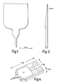
- a sensor consists of a silicon base forming an approximately square body of about 2 mm side from which projects a shank about 700 micrometers in length, 100 micrometers wide and 15 micrometers in depth, tapering to a sharp edge at its extremity as is shown in the side view of Figure 2.
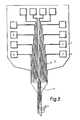
- Figure 3 shows the arrangement of conductors in the sensor.
- the shank 2 is provided along one edge with a row of twelve sensor interfaces 3 at 50 ⁇ m intervals and each interface is connected by a separate conductor 4 to a respective contact pad 5.
- Each interface is of dimensions in the range 1-2 ⁇ .
- the view of Figure 3 is taken before the final stage of manufacture which comprises coating the conductors and the surface of the body with an insulating and protective layer leaving exposed only the sensor interfaces 3 at the very edge of the shank of the sensor and a window over each of the contact areas 5 indicated by the dotted outlines 6.
- lithography is used to mask the conductors and the unmasked surface of the wafer is etched with an etchant which has a strongly preferred direction of action along a particular crystallographic axis.
- an etchant which has a strongly preferred direction of action along a particular crystallographic axis.
- Such a highly anisotropic etchant may consist, for example, of ethylene diamine, pyrocatechol and water.
- the photoresist is then removed with a suitable solvent from the surface of the upstanding sensor and this surface of the wafer is attached with black wax to a teflon paddle.
- the wafer mounted on its paddle is then immersed into an isotropic further etchant solution which etches away the silicon from the rear until the sensor is separated from the wafer, remaining fixed by the wax to the teflon paddle.
- the sensor is removed by dissolving the wax with an appropriate solvent.
- Figure 5a the silicon wafer 7 carries the sensors, each of which is protected by a layer of hardened photoresist 8.
- Figure 5b shows the same wafer section after it has been etched from the front surface by the anisotropic etchant, leaving the sensor upstanding as a mesa with its protective layer of photoresist, above the general level of the front surface of the wafer.
- Figure 5c shows the section of the wafer with the resist removed, and Figure 5d shows the separated sensor after the wafer has been eteched away from the rear surface by the final etch, which is isotropic.
- the sensing interfaces employed in this invention may be in the form of simple electrodes or they may incorporate various interfacing materials to produce various functions. They may comprise thermocouples of dissimilar metals for example.
Abstract
Description
- The invention relates to microenvironmental sensors, that is sensors for use in sensing environments of dimensions of the order of 10⁻³ -10⁻⁷ metres.
- A microenvironmental sensor may be in the form of a probe carrying a single sensing interface or an array of such interfaces, each interface being of micro dimensions and mounted on a substrate of the probe, the substrate having micro transverse dimensions. Typically the interface is carried on a shank portion of the probe. Such a probe is used in conjunction with signal processing circuitry.
- A typical application of microenvironmental sensors is in physiological work in which it is frequently necessary to use biosensors of extremely small physical dimensions. For example, it may be desired to sense neurological changes of electrical potential by implanting a sensing interface in a single nerve cell with minimal damage to and effect on the surrounding tissue and environment.
- Conventional microenvironmental sensors are large, they have substrates of more than 100µ wide, 25-30µ thick and sensing interfaces of dimensions more than about 10µ. These suffer from the disadvantages of disturbing and often irreversibly modifying the microenvironment into which they are placed, especially of the microenvironment around the sensing interfaces.
- An object of the present invention is to overcome this problem by providing a method of making a microenvironmental sensor of very small dimensions.
- According to the invention there is provided a method of making a microenvironmental sensor from a substrate having a crystalline structure, the method comprising applying sensor means to the substrate surface, anisotropically etching around the sensor means in accordance with the crystal orientation, to produce a required thickness of sensor, the releasing the sensor from the substrate.
- The present invention employs substrates of crystalline materials that can be etched by an etchant compatible with the material and acting anisotropically so as to etch the crystal preferentially in a certain crystallographic direction.
- Sensors made in accordance with this invention can be made precisely to dimensions of the order of 10⁻³-10⁻⁷ meters. They may have substrates at least a portion of which is of reduced width, typically less than 100µ, and reduced thickness, typically less than 20µ, and sensing interfaces thereon of reduced size, typically less than 5µ. This is especially advantageous for sensors to be used in microenvironments, especially delicate situations in which damage to and effect on the surroundings of the sensor, especially the sensing interface, must be minimised, such as in testing a physiological environment such as human, animal or plant tissue and cells. Other environments which may be tested are soils or metals.
- The preferred substrate material is silicon. Other materials which may be used are for example other group 4 elements such as germanium.
- The sensor of the invention may be fixed to a carrier which incorporates any required signal processing circuitry. Alternatively, the sensor itself may include signal processing circuitry.
- The sensor means preferably comprises conductive means such as metal or polysilicon. Preferred metals are tantalum, titanium, gold, silver, platinum, iridium, aluminium, nickel, rhodium. The conductive means may be insulated from the substrate, preferably by silicon dioxide and/or silicon nitride.
- A microenvironmental sensor according to the invention will be described in detail with reference to the following drawings, in which:-
- Figure 1 is a plan view in outline of a sensor produced according to the invention;
- Figure 2 is a side view of the shank of the sensor;
- Figure 3 is a surface view of the sensor showing an array of sensor interfaces, conductors and contact pads before the application of a final insulating and protective layer;
- Figure 4 shows a probe mounted in a carrier with three four channel amplifiers; and
- Figure 5 comprises diagrams showing successive stages in the making of a probe according to the invention.
- Referring first to Figure 1, a sensor consists of a silicon base forming an approximately square body of about 2 mm side from which projects a shank about 700 micrometers in length, 100 micrometers wide and 15 micrometers in depth, tapering to a sharp edge at its extremity as is shown in the side view of Figure 2.
- Figure 3 shows the arrangement of conductors in the sensor. The shank 2 is provided along one edge with a row of twelve sensor interfaces 3 at 50 µm intervals and each interface is connected by a separate conductor 4 to a
respective contact pad 5. Each interface is of dimensions in the range 1-2µ. The view of Figure 3 is taken before the final stage of manufacture which comprises coating the conductors and the surface of the body with an insulating and protective layer leaving exposed only the sensor interfaces 3 at the very edge of the shank of the sensor and a window over each of thecontact areas 5 indicated by the dottedoutlines 6. - When the manufacture of the sensor has been thus completed it is fitted face down into a carrier as shown in Figure 4, the carrier making contact with the twelve contact pads and connecting them to the inputs of three four-channel amplifiers f mounted in the carrier. The overall dimensions of the carrier are approximately 4.5 mm long, 2.3 mm wide and .25 mm thick. The carrier may incorporate any required signal processing circuitry.
- The sensor is made from a silicon wafer as follows.
- A pattern of conductors corresponding to a sensor corresponding to the arrangement shown in Figure 3, is formed on one surface of a silicon wafer, which may be a single crystal, by use of known techniques employed in the manufacture of integrated circuits. For example, the conductors may be laid down by vacuum deposition, sputtering or selective etching of a uniformly applied metal layer. The conductors are insulated from the silicon substrate, for example by silicon dioxide. The metal of the sensor interface must not react with the constituents of living cells. A preferred metal is gold, which is biocompatible, chemically stable and not prone to oxidation. The gold is adhered to the conductor via a layer of chrome. The conductors of the sensor are finally protected by an insulating and protective layer, as already described with reference to Figure 3.
- When the conductors and insulators of the sensor have been formed in this way or prior to this, a layer of photoresist is applied to the surface of the silicon wafer and exposed through a mask so as to define the outlines of the sensor as shown in Figure 1. Then the unexposed portions of the photoresist are dissolved away.
- Further lithography is used to mask the conductors and the unmasked surface of the wafer is etched with an etchant which has a strongly preferred direction of action along a particular crystallographic axis. Such a highly anisotropic etchant may consist, for example, of ethylene diamine, pyrocatechol and water. By the use of this etchant the unmasked silicon surrounding the probes is etched away, leaving the sensors upstanding as mesas above the surrounding surface.
- The photoresist is then removed with a suitable solvent from the surface of the upstanding sensor and this surface of the wafer is attached with black wax to a teflon paddle. The wafer mounted on its paddle is then immersed into an isotropic further etchant solution which etches away the silicon from the rear until the sensor is separated from the wafer, remaining fixed by the wax to the teflon paddle. In the final stage of the manufacture, the sensor is removed by dissolving the wax with an appropriate solvent.
- The final etching stages are shown diagrammatically in Figure 5. In Figure 5a the
silicon wafer 7 carries the sensors, each of which is protected by a layer of hardenedphotoresist 8. Figure 5b shows the same wafer section after it has been etched from the front surface by the anisotropic etchant, leaving the sensor upstanding as a mesa with its protective layer of photoresist, above the general level of the front surface of the wafer. Figure 5c shows the section of the wafer with the resist removed, and Figure 5d shows the separated sensor after the wafer has been eteched away from the rear surface by the final etch, which is isotropic. - More than one sensor may be made from a single wafer as shown in Figure 5.
- The sensing interfaces employed in this invention may be in the form of simple electrodes or they may incorporate various interfacing materials to produce various functions. They may comprise thermocouples of dissimilar metals for example.
Claims (16)
Applications Claiming Priority (4)
| Application Number | Priority Date | Filing Date | Title |
|---|---|---|---|
| GB8702066 | 1987-01-30 | ||
| GB878702066A GB8702066D0 (en) | 1987-01-30 | 1987-01-30 | Microenvironmental sensors |
| GB878728102A GB8728102D0 (en) | 1987-12-01 | 1987-12-01 | Microenvironmental sensors |
| GB8728102 | 1987-12-01 |
Publications (2)
| Publication Number | Publication Date |
|---|---|
| EP0276979A2 true EP0276979A2 (en) | 1988-08-03 |
| EP0276979A3 EP0276979A3 (en) | 1989-12-06 |
Family
ID=26291849
Family Applications (1)
| Application Number | Title | Priority Date | Filing Date |
|---|---|---|---|
| EP88300624A Withdrawn EP0276979A3 (en) | 1987-01-30 | 1988-01-26 | Microenvironmental sensors |
Country Status (3)
| Country | Link |
|---|---|
| US (1) | US5020376A (en) |
| EP (1) | EP0276979A3 (en) |
| JP (1) | JPS63282645A (en) |
Cited By (3)
| Publication number | Priority date | Publication date | Assignee | Title |
|---|---|---|---|---|
| EP0774917A1 (en) * | 1994-08-12 | 1997-05-28 | Cb Carmel Biotechnology, Ltd. | Implantable sensor chip |
| AT403528B (en) * | 1989-04-04 | 1998-03-25 | Urban Gerald | MICRO-MULTI-ELECTRODE STRUCTURE FOR ELECTROCHEMICAL APPLICATIONS AND METHOD FOR THEIR PRODUCTION |
| EP2393424A2 (en) * | 2009-02-09 | 2011-12-14 | Edwards Lifesciences Corporation | Analyte sensor and fabrication methods |
Families Citing this family (2)
| Publication number | Priority date | Publication date | Assignee | Title |
|---|---|---|---|---|
| US5267471A (en) * | 1992-04-30 | 1993-12-07 | Ibm Corporation | Double cantilever sensor for atomic force microscope |
| CN104132965B (en) * | 2014-07-11 | 2016-03-09 | 江西科技师范大学 | Polygalic acid is to the test method of the effect that hippocampus of rats cynapse is transmitted |
Citations (1)
| Publication number | Priority date | Publication date | Assignee | Title |
|---|---|---|---|---|
| US4461304A (en) * | 1979-11-05 | 1984-07-24 | Massachusetts Institute Of Technology | Microelectrode and assembly for parallel recording of neurol groups |
Family Cites Families (11)
| Publication number | Priority date | Publication date | Assignee | Title |
|---|---|---|---|---|
| NL255453A (en) * | 1960-02-04 | |||
| US3288662A (en) * | 1963-07-18 | 1966-11-29 | Rca Corp | Method of etching to dice a semiconductor slice |
| GB1251692A (en) * | 1968-03-29 | 1971-10-27 | ||
| IT1125182B (en) * | 1976-12-14 | 1986-05-14 | Selenia Ind Elettroniche | PROCEDURE FOR THE PRODUCTION OF LINEAR AND TWO-DIMENSIONAL INFRARED DETECTORS FOR MULTI-ELEMENTS WITH PERFECTED GEOMETRIC CHARACTERISTICS AND HIGH DEGREE OF INTEGRATION |
| US4129042A (en) * | 1977-11-18 | 1978-12-12 | Signetics Corporation | Semiconductor transducer packaged assembly |
| US4793194A (en) * | 1985-03-26 | 1988-12-27 | Endevco Corporation | Piezoresistive transducer |
| US4766666A (en) * | 1985-09-30 | 1988-08-30 | Kabushiki Kaisha Toyota Chuo Kenkyusho | Semiconductor pressure sensor and method of manufacturing the same |
| DE3606851A1 (en) * | 1986-03-03 | 1987-09-10 | Vdo Schindling | ARRANGEMENT FOR MEASURING THE FLOW RATE |
| US4682503A (en) * | 1986-05-16 | 1987-07-28 | Honeywell Inc. | Microscopic size, thermal conductivity type, air or gas absolute pressure sensor |
| US4872945A (en) * | 1986-06-25 | 1989-10-10 | Motorola Inc. | Post seal etching of transducer diaphragm |
| US4790192A (en) * | 1987-09-24 | 1988-12-13 | Rosemount Inc. | Silicon side by side coplanar pressure sensors |
-
1988
- 1988-01-26 EP EP88300624A patent/EP0276979A3/en not_active Withdrawn
- 1988-01-29 JP JP63017545A patent/JPS63282645A/en active Pending
- 1988-01-29 US US07/149,847 patent/US5020376A/en not_active Expired - Fee Related
Patent Citations (1)
| Publication number | Priority date | Publication date | Assignee | Title |
|---|---|---|---|---|
| US4461304A (en) * | 1979-11-05 | 1984-07-24 | Massachusetts Institute Of Technology | Microelectrode and assembly for parallel recording of neurol groups |
Non-Patent Citations (2)
| Title |
|---|
| IBM TECHNICAL DISCLOSURE BULLETIN * |
| IEEE TRANSACTIONS ON BIOMEDICAL ENGINEERING * |
Cited By (6)
| Publication number | Priority date | Publication date | Assignee | Title |
|---|---|---|---|---|
| AT403528B (en) * | 1989-04-04 | 1998-03-25 | Urban Gerald | MICRO-MULTI-ELECTRODE STRUCTURE FOR ELECTROCHEMICAL APPLICATIONS AND METHOD FOR THEIR PRODUCTION |
| EP0774917A1 (en) * | 1994-08-12 | 1997-05-28 | Cb Carmel Biotechnology, Ltd. | Implantable sensor chip |
| EP0774917A4 (en) * | 1994-08-12 | 1997-10-15 | Cb Carmel Biotechnology Ltd | Implantable sensor chip |
| EP2393424A2 (en) * | 2009-02-09 | 2011-12-14 | Edwards Lifesciences Corporation | Analyte sensor and fabrication methods |
| EP2393424A4 (en) * | 2009-02-09 | 2013-06-05 | Edwards Lifesciences Corp | Analyte sensor and fabrication methods |
| US8696917B2 (en) | 2009-02-09 | 2014-04-15 | Edwards Lifesciences Corporation | Analyte sensor and fabrication methods |
Also Published As
| Publication number | Publication date |
|---|---|
| EP0276979A3 (en) | 1989-12-06 |
| JPS63282645A (en) | 1988-11-18 |
| US5020376A (en) | 1991-06-04 |
Similar Documents
| Publication | Publication Date | Title |
|---|---|---|
| Yoon et al. | A micromachined silicon depth probe for multichannel neural recording | |
| Hoogerwerf et al. | A three-dimensional microelectrode array for chronic neural recording | |
| Najafi et al. | A high-yield IC-compatible multichannel recording array | |
| US6973342B1 (en) | Flexible bio-probe assembly | |
| US8637351B2 (en) | Methods for making micro needles and applications thereof | |
| US11022577B2 (en) | Nanopatterned biosensor electrode for enhanced sensor signal and sensitivity | |
| US4765865A (en) | Silicon etch rate enhancement | |
| US4783237A (en) | Solid state transducer and method of making same | |
| Ensell et al. | Silicon-based microelectrodes for neurophysiology fabricated using a gold metallization/nitride passivation system | |
| US11013437B2 (en) | Nanopatterned biosensor electrode for enhanced sensor signal and sensitivity | |
| Ensell | Free standing single-crystal silicon microstructures | |
| US20060213259A1 (en) | Sensors for electrochemical, electrical or topographical analysis | |
| US20070187238A1 (en) | Microelectrode system for neuro-stimulation and neuro-sensing and microchip packaging | |
| Van den Vlekkert et al. | A pH-ISFET and an integrated pH-pressure sensor with back-side contacts | |
| EP0276979A2 (en) | Microenvironmental sensors | |
| Ensell et al. | Silicon-based microelectrodes for neurophysiology, micromachined from silicon-on-insulator wafers | |
| US6719582B1 (en) | Method of making a flexible electrode bio-probe assembly | |
| Kawano et al. | Multichannel 5× 5-Site 3-dimensional Si microprobe electrode array for neural activity recording system | |
| US20130190586A1 (en) | Multi-Terminal Nanoelectrode Array | |
| Peeters et al. | A two-wire, digital output multichannel microprobe for recording single-unit neural activity | |
| JPS6242539A (en) | Chemically responsive semiconductor device and manufacture thereof | |
| JPH02221881A (en) | Probe for testing integrated circuit device | |
| KR100277533B1 (en) | Needle type sensor and manufacturing method thereof | |
| Metz et al. | Microelectrodes with three-dimensional structures for improved neural interfacing | |
| JPH0843344A (en) | Micro-array carbon electrode and its manufacture |
Legal Events
| Date | Code | Title | Description |
|---|---|---|---|
| PUAI | Public reference made under article 153(3) epc to a published international application that has entered the european phase |
Free format text: ORIGINAL CODE: 0009012 |
|
| AK | Designated contracting states |
Kind code of ref document: A2 Designated state(s): AT BE CH DE ES FR GB GR IT LI LU NL SE |
|
| PUAL | Search report despatched |
Free format text: ORIGINAL CODE: 0009013 |
|
| AK | Designated contracting states |
Kind code of ref document: A3 Designated state(s): AT BE CH DE ES FR GB GR IT LI LU NL SE |
|
| RHK1 | Main classification (correction) |
Ipc: A61B 5/04 |
|
| RIN1 | Information on inventor provided before grant (corrected) |
Inventor name: ENSELL, GRAHAM, DR.C/OUNIVERSITY COLLEGE CARDIFF Inventor name: LEONG, DAVID,C/O UNIVERSITY COLLEGE CARDIFF Inventor name: PICKARD, ROBERT S., PROF. Inventor name: WALL, PETER, DR. |
|
| 17P | Request for examination filed |
Effective date: 19900606 |
|
| 17Q | First examination report despatched |
Effective date: 19920313 |
|
| STAA | Information on the status of an ep patent application or granted ep patent |
Free format text: STATUS: THE APPLICATION IS DEEMED TO BE WITHDRAWN |
|
| 18D | Application deemed to be withdrawn |
Effective date: 19930306 |