EP0266210A2 - Electronic apparatus comprising a ceramic substrate - Google Patents
Electronic apparatus comprising a ceramic substrate Download PDFInfo
- Publication number
- EP0266210A2 EP0266210A2 EP87309593A EP87309593A EP0266210A2 EP 0266210 A2 EP0266210 A2 EP 0266210A2 EP 87309593 A EP87309593 A EP 87309593A EP 87309593 A EP87309593 A EP 87309593A EP 0266210 A2 EP0266210 A2 EP 0266210A2
- Authority
- EP
- European Patent Office
- Prior art keywords
- wiring portion
- ceramic substrate
- multilayered wiring
- main surface
- layer
- Prior art date
- Legal status (The legal status is an assumption and is not a legal conclusion. Google has not performed a legal analysis and makes no representation as to the accuracy of the status listed.)
- Granted
Links
Images


Classifications
-
- H—ELECTRICITY
- H01—ELECTRIC ELEMENTS
- H01L—SEMICONDUCTOR DEVICES NOT COVERED BY CLASS H10
- H01L23/00—Details of semiconductor or other solid state devices
- H01L23/02—Containers; Seals
- H01L23/10—Containers; Seals characterised by the material or arrangement of seals between parts, e.g. between cap and base of the container or between leads and walls of the container
-
- H—ELECTRICITY
- H01—ELECTRIC ELEMENTS
- H01L—SEMICONDUCTOR DEVICES NOT COVERED BY CLASS H10
- H01L23/00—Details of semiconductor or other solid state devices
- H01L23/02—Containers; Seals
- H01L23/04—Containers; Seals characterised by the shape of the container or parts, e.g. caps, walls
- H01L23/053—Containers; Seals characterised by the shape of the container or parts, e.g. caps, walls the container being a hollow construction and having an insulating or insulated base as a mounting for the semiconductor body
- H01L23/057—Containers; Seals characterised by the shape of the container or parts, e.g. caps, walls the container being a hollow construction and having an insulating or insulated base as a mounting for the semiconductor body the leads being parallel to the base
-
- H—ELECTRICITY
- H01—ELECTRIC ELEMENTS
- H01L—SEMICONDUCTOR DEVICES NOT COVERED BY CLASS H10
- H01L23/00—Details of semiconductor or other solid state devices
- H01L23/52—Arrangements for conducting electric current within the device in operation from one component to another, i.e. interconnections, e.g. wires, lead frames
- H01L23/538—Arrangements for conducting electric current within the device in operation from one component to another, i.e. interconnections, e.g. wires, lead frames the interconnection structure between a plurality of semiconductor chips being formed on, or in, insulating substrates
-
- H—ELECTRICITY
- H01—ELECTRIC ELEMENTS
- H01L—SEMICONDUCTOR DEVICES NOT COVERED BY CLASS H10
- H01L25/00—Assemblies consisting of a plurality of individual semiconductor or other solid state devices ; Multistep manufacturing processes thereof
- H01L25/16—Assemblies consisting of a plurality of individual semiconductor or other solid state devices ; Multistep manufacturing processes thereof the devices being of types provided for in two or more different main groups of groups H01L27/00 - H01L33/00, or in a single subclass of H10K, H10N, e.g. forming hybrid circuits
-
- H—ELECTRICITY
- H01—ELECTRIC ELEMENTS
- H01L—SEMICONDUCTOR DEVICES NOT COVERED BY CLASS H10
- H01L2224/00—Indexing scheme for arrangements for connecting or disconnecting semiconductor or solid-state bodies and methods related thereto as covered by H01L24/00
- H01L2224/01—Means for bonding being attached to, or being formed on, the surface to be connected, e.g. chip-to-package, die-attach, "first-level" interconnects; Manufacturing methods related thereto
- H01L2224/26—Layer connectors, e.g. plate connectors, solder or adhesive layers; Manufacturing methods related thereto
- H01L2224/31—Structure, shape, material or disposition of the layer connectors after the connecting process
- H01L2224/32—Structure, shape, material or disposition of the layer connectors after the connecting process of an individual layer connector
- H01L2224/321—Disposition
- H01L2224/32151—Disposition the layer connector connecting between a semiconductor or solid-state body and an item not being a semiconductor or solid-state body, e.g. chip-to-substrate, chip-to-passive
- H01L2224/32221—Disposition the layer connector connecting between a semiconductor or solid-state body and an item not being a semiconductor or solid-state body, e.g. chip-to-substrate, chip-to-passive the body and the item being stacked
- H01L2224/32225—Disposition the layer connector connecting between a semiconductor or solid-state body and an item not being a semiconductor or solid-state body, e.g. chip-to-substrate, chip-to-passive the body and the item being stacked the item being non-metallic, e.g. insulating substrate with or without metallisation
-
- H—ELECTRICITY
- H01—ELECTRIC ELEMENTS
- H01L—SEMICONDUCTOR DEVICES NOT COVERED BY CLASS H10
- H01L2224/00—Indexing scheme for arrangements for connecting or disconnecting semiconductor or solid-state bodies and methods related thereto as covered by H01L24/00
- H01L2224/01—Means for bonding being attached to, or being formed on, the surface to be connected, e.g. chip-to-package, die-attach, "first-level" interconnects; Manufacturing methods related thereto
- H01L2224/42—Wire connectors; Manufacturing methods related thereto
- H01L2224/44—Structure, shape, material or disposition of the wire connectors prior to the connecting process
- H01L2224/45—Structure, shape, material or disposition of the wire connectors prior to the connecting process of an individual wire connector
- H01L2224/45001—Core members of the connector
- H01L2224/45099—Material
- H01L2224/451—Material with a principal constituent of the material being a metal or a metalloid, e.g. boron (B), silicon (Si), germanium (Ge), arsenic (As), antimony (Sb), tellurium (Te) and polonium (Po), and alloys thereof
- H01L2224/45117—Material with a principal constituent of the material being a metal or a metalloid, e.g. boron (B), silicon (Si), germanium (Ge), arsenic (As), antimony (Sb), tellurium (Te) and polonium (Po), and alloys thereof the principal constituent melting at a temperature of greater than or equal to 400°C and less than 950°C
- H01L2224/45124—Aluminium (Al) as principal constituent
-
- H—ELECTRICITY
- H01—ELECTRIC ELEMENTS
- H01L—SEMICONDUCTOR DEVICES NOT COVERED BY CLASS H10
- H01L2224/00—Indexing scheme for arrangements for connecting or disconnecting semiconductor or solid-state bodies and methods related thereto as covered by H01L24/00
- H01L2224/01—Means for bonding being attached to, or being formed on, the surface to be connected, e.g. chip-to-package, die-attach, "first-level" interconnects; Manufacturing methods related thereto
- H01L2224/42—Wire connectors; Manufacturing methods related thereto
- H01L2224/44—Structure, shape, material or disposition of the wire connectors prior to the connecting process
- H01L2224/45—Structure, shape, material or disposition of the wire connectors prior to the connecting process of an individual wire connector
- H01L2224/45001—Core members of the connector
- H01L2224/45099—Material
- H01L2224/451—Material with a principal constituent of the material being a metal or a metalloid, e.g. boron (B), silicon (Si), germanium (Ge), arsenic (As), antimony (Sb), tellurium (Te) and polonium (Po), and alloys thereof
- H01L2224/45138—Material with a principal constituent of the material being a metal or a metalloid, e.g. boron (B), silicon (Si), germanium (Ge), arsenic (As), antimony (Sb), tellurium (Te) and polonium (Po), and alloys thereof the principal constituent melting at a temperature of greater than or equal to 950°C and less than 1550°C
- H01L2224/45144—Gold (Au) as principal constituent
-
- H—ELECTRICITY
- H01—ELECTRIC ELEMENTS
- H01L—SEMICONDUCTOR DEVICES NOT COVERED BY CLASS H10
- H01L2224/00—Indexing scheme for arrangements for connecting or disconnecting semiconductor or solid-state bodies and methods related thereto as covered by H01L24/00
- H01L2224/01—Means for bonding being attached to, or being formed on, the surface to be connected, e.g. chip-to-package, die-attach, "first-level" interconnects; Manufacturing methods related thereto
- H01L2224/42—Wire connectors; Manufacturing methods related thereto
- H01L2224/47—Structure, shape, material or disposition of the wire connectors after the connecting process
- H01L2224/48—Structure, shape, material or disposition of the wire connectors after the connecting process of an individual wire connector
- H01L2224/4805—Shape
- H01L2224/4809—Loop shape
- H01L2224/48091—Arched
-
- H—ELECTRICITY
- H01—ELECTRIC ELEMENTS
- H01L—SEMICONDUCTOR DEVICES NOT COVERED BY CLASS H10
- H01L2224/00—Indexing scheme for arrangements for connecting or disconnecting semiconductor or solid-state bodies and methods related thereto as covered by H01L24/00
- H01L2224/01—Means for bonding being attached to, or being formed on, the surface to be connected, e.g. chip-to-package, die-attach, "first-level" interconnects; Manufacturing methods related thereto
- H01L2224/42—Wire connectors; Manufacturing methods related thereto
- H01L2224/47—Structure, shape, material or disposition of the wire connectors after the connecting process
- H01L2224/48—Structure, shape, material or disposition of the wire connectors after the connecting process of an individual wire connector
- H01L2224/481—Disposition
- H01L2224/48151—Connecting between a semiconductor or solid-state body and an item not being a semiconductor or solid-state body, e.g. chip-to-substrate, chip-to-passive
- H01L2224/48221—Connecting between a semiconductor or solid-state body and an item not being a semiconductor or solid-state body, e.g. chip-to-substrate, chip-to-passive the body and the item being stacked
- H01L2224/48225—Connecting between a semiconductor or solid-state body and an item not being a semiconductor or solid-state body, e.g. chip-to-substrate, chip-to-passive the body and the item being stacked the item being non-metallic, e.g. insulating substrate with or without metallisation
- H01L2224/48227—Connecting between a semiconductor or solid-state body and an item not being a semiconductor or solid-state body, e.g. chip-to-substrate, chip-to-passive the body and the item being stacked the item being non-metallic, e.g. insulating substrate with or without metallisation connecting the wire to a bond pad of the item
-
- H—ELECTRICITY
- H01—ELECTRIC ELEMENTS
- H01L—SEMICONDUCTOR DEVICES NOT COVERED BY CLASS H10
- H01L2224/00—Indexing scheme for arrangements for connecting or disconnecting semiconductor or solid-state bodies and methods related thereto as covered by H01L24/00
- H01L2224/01—Means for bonding being attached to, or being formed on, the surface to be connected, e.g. chip-to-package, die-attach, "first-level" interconnects; Manufacturing methods related thereto
- H01L2224/42—Wire connectors; Manufacturing methods related thereto
- H01L2224/47—Structure, shape, material or disposition of the wire connectors after the connecting process
- H01L2224/48—Structure, shape, material or disposition of the wire connectors after the connecting process of an individual wire connector
- H01L2224/484—Connecting portions
- H01L2224/48463—Connecting portions the connecting portion on the bonding area of the semiconductor or solid-state body being a ball bond
- H01L2224/48465—Connecting portions the connecting portion on the bonding area of the semiconductor or solid-state body being a ball bond the other connecting portion not on the bonding area being a wedge bond, i.e. ball-to-wedge, regular stitch
-
- H—ELECTRICITY
- H01—ELECTRIC ELEMENTS
- H01L—SEMICONDUCTOR DEVICES NOT COVERED BY CLASS H10
- H01L2224/00—Indexing scheme for arrangements for connecting or disconnecting semiconductor or solid-state bodies and methods related thereto as covered by H01L24/00
- H01L2224/73—Means for bonding being of different types provided for in two or more of groups H01L2224/10, H01L2224/18, H01L2224/26, H01L2224/34, H01L2224/42, H01L2224/50, H01L2224/63, H01L2224/71
- H01L2224/732—Location after the connecting process
- H01L2224/73251—Location after the connecting process on different surfaces
- H01L2224/73265—Layer and wire connectors
-
- H—ELECTRICITY
- H01—ELECTRIC ELEMENTS
- H01L—SEMICONDUCTOR DEVICES NOT COVERED BY CLASS H10
- H01L24/00—Arrangements for connecting or disconnecting semiconductor or solid-state bodies; Methods or apparatus related thereto
- H01L24/01—Means for bonding being attached to, or being formed on, the surface to be connected, e.g. chip-to-package, die-attach, "first-level" interconnects; Manufacturing methods related thereto
- H01L24/42—Wire connectors; Manufacturing methods related thereto
- H01L24/44—Structure, shape, material or disposition of the wire connectors prior to the connecting process
- H01L24/45—Structure, shape, material or disposition of the wire connectors prior to the connecting process of an individual wire connector
-
- H—ELECTRICITY
- H01—ELECTRIC ELEMENTS
- H01L—SEMICONDUCTOR DEVICES NOT COVERED BY CLASS H10
- H01L24/00—Arrangements for connecting or disconnecting semiconductor or solid-state bodies; Methods or apparatus related thereto
- H01L24/01—Means for bonding being attached to, or being formed on, the surface to be connected, e.g. chip-to-package, die-attach, "first-level" interconnects; Manufacturing methods related thereto
- H01L24/42—Wire connectors; Manufacturing methods related thereto
- H01L24/47—Structure, shape, material or disposition of the wire connectors after the connecting process
- H01L24/48—Structure, shape, material or disposition of the wire connectors after the connecting process of an individual wire connector
-
- H—ELECTRICITY
- H01—ELECTRIC ELEMENTS
- H01L—SEMICONDUCTOR DEVICES NOT COVERED BY CLASS H10
- H01L2924/00—Indexing scheme for arrangements or methods for connecting or disconnecting semiconductor or solid-state bodies as covered by H01L24/00
- H01L2924/01—Chemical elements
- H01L2924/01046—Palladium [Pd]
-
- H—ELECTRICITY
- H01—ELECTRIC ELEMENTS
- H01L—SEMICONDUCTOR DEVICES NOT COVERED BY CLASS H10
- H01L2924/00—Indexing scheme for arrangements or methods for connecting or disconnecting semiconductor or solid-state bodies as covered by H01L24/00
- H01L2924/01—Chemical elements
- H01L2924/01078—Platinum [Pt]
-
- H—ELECTRICITY
- H01—ELECTRIC ELEMENTS
- H01L—SEMICONDUCTOR DEVICES NOT COVERED BY CLASS H10
- H01L2924/00—Indexing scheme for arrangements or methods for connecting or disconnecting semiconductor or solid-state bodies as covered by H01L24/00
- H01L2924/01—Chemical elements
- H01L2924/01079—Gold [Au]
-
- H—ELECTRICITY
- H01—ELECTRIC ELEMENTS
- H01L—SEMICONDUCTOR DEVICES NOT COVERED BY CLASS H10
- H01L2924/00—Indexing scheme for arrangements or methods for connecting or disconnecting semiconductor or solid-state bodies as covered by H01L24/00
- H01L2924/013—Alloys
- H01L2924/0132—Binary Alloys
- H01L2924/01322—Eutectic Alloys, i.e. obtained by a liquid transforming into two solid phases
-
- H—ELECTRICITY
- H01—ELECTRIC ELEMENTS
- H01L—SEMICONDUCTOR DEVICES NOT COVERED BY CLASS H10
- H01L2924/00—Indexing scheme for arrangements or methods for connecting or disconnecting semiconductor or solid-state bodies as covered by H01L24/00
- H01L2924/095—Indexing scheme for arrangements or methods for connecting or disconnecting semiconductor or solid-state bodies as covered by H01L24/00 with a principal constituent of the material being a combination of two or more materials provided in the groups H01L2924/013 - H01L2924/0715
- H01L2924/097—Glass-ceramics, e.g. devitrified glass
- H01L2924/09701—Low temperature co-fired ceramic [LTCC]
-
- H—ELECTRICITY
- H01—ELECTRIC ELEMENTS
- H01L—SEMICONDUCTOR DEVICES NOT COVERED BY CLASS H10
- H01L2924/00—Indexing scheme for arrangements or methods for connecting or disconnecting semiconductor or solid-state bodies as covered by H01L24/00
- H01L2924/15—Details of package parts other than the semiconductor or other solid state devices to be connected
- H01L2924/161—Cap
- H01L2924/1615—Shape
- H01L2924/16152—Cap comprising a cavity for hosting the device, e.g. U-shaped cap
-
- H—ELECTRICITY
- H01—ELECTRIC ELEMENTS
- H01L—SEMICONDUCTOR DEVICES NOT COVERED BY CLASS H10
- H01L2924/00—Indexing scheme for arrangements or methods for connecting or disconnecting semiconductor or solid-state bodies as covered by H01L24/00
- H01L2924/19—Details of hybrid assemblies other than the semiconductor or other solid state devices to be connected
- H01L2924/1901—Structure
- H01L2924/1904—Component type
- H01L2924/19041—Component type being a capacitor
Definitions
- This invention relates to an electronic apparatus and more particularly to an electronic apparatus of the type which, like a hybrid IC, has electronic devices mounted on a multilayer substrate and covered with a hermetic cap.
- hybrid IC's constructed by mounting numerous chip components such as IC chips, resistors, and capacitors on a multilayer ceramic substrate and hermetically covering these chip components with a metallic cap are finding increasing applications.
- the ceramic multilayer substrates which are used for such hybrid IC's have been heretofore produced by the green sheet method, the thick film method, or the mixed thick film-thin film method.
- This multilayer substrate has a construction in which, as illustrated in Fig. 1, a thin-film conductor pattern 1 formed mainly of copper in a thickness of about 1 to 10 ⁇ m, generally 1 to 3 ⁇ m and a polyimide layer 2 having the thickness of about 10 ⁇ m are alternately superposed a plurality of times on a ceramic substrate 3. It is produced as follows.
- the thin-film conductor pattern is formed by evaporating or spattering copper land a conductive metal other than copper thereby supperposing a conductor layer on the entire surface of the ceramic substrate 3 and etching unnecessary portions by the photolithographic technique. Then, on this thin-film conductor pattern, polyimide is deposited in the form of a thin layer by spin coating and this thin layer is dried. By photolithography, via holes 4 are formed to interconnect the upper and lower conductor patterns 1 electrically. By repeating this procedure a plurality of times, there is obtained a copper-polyimide multilayer substrate.
- This copper-polyimide multilayer substrate has a disadvantage that the polyimide resin used therein is hygroscopic.
- the hybrid IC which is produced by mounting IC chips on this substrate and hermetically sealing the IC chips with a metallic cap, therefore, suffers moisture to permeate through the polyimide layer 2 and reach the interior of the metallic cap.
- the conventional hybrid IC's using this copper-polyimide multilayer substrate have had the disadvantage that the humidity reaching the interior of the metallic cap through the polyimide layer 2 will expose the multilayered wiring portion to the danger of forming closed-circuit failure through migration, the IC chips and bonding wires to the danger of yielding to corrosion, and the entire IC proper to the danger of establishing closed-circuit failure due to formation of dew during the course of the temperature cycling test.
- a primary object of this invention is to provide an electronic apparatus constructed that the IC chips mounted on the substrate thereof will operate at high speeds, the portion hermetically sealed with a cap will not admit moisture, and the danger of migration, the danger of wire corrosion, the danger of dew formation, and the danger of estabilishment of closed-circuit failure due to formation of dew during the course of temperature cycling test will never happen.
- Another object of this invention is to provide an electronic apparatus incorporating therein an input-output conductor pad which enables a metallic cap, input and output leads, and input and output pins to be fixed thereto with full strength.
- the electronic apparatus of this invention comprises a ceramic substrate, a multilayered wiring portion disposed at a distance from the periphery of the main surface of the ceramic substrate and produced by althernately repeating a conductor pattern formed by the thin-film method using a conductive metal and a polyimide layer, electronic devices mounted on the multilayered wiring portion and electrically connected to the conductor patterns of the multilayered wiring portion, input and output conductor pads formed on the periphery of the main surface of the ceramic substrate, connection conductor patterns formed on the main surface of the ceramic substrate astride the gap between the line patterns of the multilayered wiring portion and the input and output conductor pads, an inorganic insulation layer formed annularly on the main surface of the ceramic substrate across over at least part of the connection conductor patterns around the multilayered wiring portion, a metallized layer formed on the inorganic insulation layer, and a moistureproof cap having the edge thereof hermetically fixed by soldering on the metallized layer.
- the ceramic substrate mentioned above there can be used an alumina substrate or an A1N substrate, for example.
- the conductor pattern as the first layer in the multilayered wiring portion is formed, for example, by forming a conductive metal coat on the entire surface of a ceramic substrate by the thin-film method, i.e. by evaporating or spattering a conductive metal such as Cr/Cu, Ti/Cu, Cr/Cu/Cr, Ti/Cu/Ti, Cr/Cu/Au, or Ti/Cu/Au which has copper as a main component and etching the conductive metal coat in a prescribed pattern by the photolithographic method.
- the conductor pattern as the lowermost layer is formed in such a manner that the edges thereof will be superposed on the inner edges of the connection conductor patterns which will be described more fully later on and is electrically connected to the connection conductor patterns.
- the polyimide layer superposed on the thin-film conductor pattern is formed, for example, by applying a photosensitive polyimide resin in the form of a thin film by spin coating on the aforementioned conductor pattern, drying the applied film of the polyimide resin, and etching the dry film photolighographically in such a manner as to impart via holes and a visible contour thereto.
- the multilayered wiring portion is formed by alternately repeating the aforementioned thin-film conductor pattern and polyimide layer a plurality of times.
- the input and output conductor pads and the connection conductor patterns are generally formed by superposing a pasty conductive composition on the ceramic substrate by the thick-film method, i.e. by printing the pasty conductive composition in prescribed patterns by the screen printing method and drying and firing the deposited layers of the composition.
- a pasty conductive composition suitably used by the thick-film method
- there may be cited Cu paste, Ag-Pt paste, Au-Pt paste, and Ag-Pd paste which exhibit satisfactory wettability and low diffusibility to the Sn-Pb type solder.
- the thickness which the input and output conductor pads and the connection conductor patterns will assume after the firing are approximately in the range of 1 to 20 ⁇ m.
- the thick-film method described herein has generally two process as follows.
- a photosensitive layer is formed by applying a photosensitive emulsion on a screen having generally 325 mesh and drying the screen. Then this photosensitive layer is exposed by using a mask and developed. Thereby, this layer is partially removed. Setting the obtained screen on the substrate and printing by using a pasty conductive composition, this pasty composition is printed on the screen only to the part which the photosensitive layer is partially removed.
- This process can be used for forming a conductor pattern generally having the line width of about 100 ⁇ m or more and the thickness in the range of 10 to 15 ⁇ m.
- the pasty conductive composition is printed on the substrate in the thin layer state by using the screen having generally 400 mesh.
- This layer of pasty conductive composition is dried and fired, thereby caused a uniformed conductor layer.
- this conductor layer is etched by the photolithographic technique. Thereby, the prescribed conductor pattern can be obtained.
- This process can be used for forming a fine conductor pattern generally having the line width in the range of 30 to 50 ⁇ m and the thickness in the range of 3 to 5 ⁇ m.
- the input and output conductor pads may be formed in combination with the conductor pattern as the uppermost layer of the multilayered wiring portion, subsequently to the formation of the connecting conductor patterns by the thick-film method, in accordance with the thin-film method applying the aforementioned conductive metal composed mainly of copper in such a manner as to overlie the outer edges of the connection conductor patterns.
- the input and output conductor pads may be otherwise obtained by first forming the conductor metal in a prescribed shape by the thick-film method using an Au paste in such a manner as to come into contact with the outer edges of the connection conductor patterns and then coating the deposited layer of the conductor metal with a metal layer formed mainly of copper by the thin-film method.
- the annular inorganic insulation layer to be formed across the connection conductor patterns it is suitable to use what is produced in a thickness in the range of 10 to 40 ⁇ m by the so-called thick-film method which comprises applying an inorganic insulator paste such as crystallized glass or ceramic in a prescribed pattern on a surface by screen printing and then firing the applied layer.
- the annular metallized layer to be formed on the inorganic insulation layer is destined to function as a seal ring pattern while a hermetic cap such as the metallic cap disposed to enclose such devices as IC chips mounted on the multilayered wiring portion is fixed by fusion with a solder. It is superposed on the inorganic insulation layer by the thick-film method using either the aforementioned pasty conductive composition or a pasty conductive composition containing metal powder, metal oxide, etc.
- annular metallized layer and the input and output conductor pads are formed by the thick-film method specifically using a pasty conductive composition which exhibits satisfactory wettability to the Sn-Pb type solder and diffuses at a low speed in this solder, there is derived the advantage that the layer and the pads so produced will increase the strength of fixation and facilitate the work of soldering when the metallic cap, input and output leads, or input and output pins are to be fixed thereon as with a solder.
- the aforementioned conductive metal composed mainly of copper may be applied by the thin-film method so as to coat completely the thick-film layers.
- the thin-film coats thus added further enhance the strength of fixation and further facilitate the work of soldering when the moistureproof cap, inlet and outlet leads, and input and output pins are to be fixed thereon as with a solder.
- the IC chips and the electronic chip components such as resistors and capacitors are mounted on the multilayered wiring portion by a suitable conventional method such as, for example, the wire bonding method or the method of electric connection using bumps and no wire.
- a moistureproof cap such as the metallic cap is hermetically deposited by soldering.
- the metallic cap can be fixed hermetically with the upper side of the annular metallized layer by soldering. Moreover, since the inorganic insulation layer completely outside the seal ring pattern is formed of ceramic or crystallized glass, there is absolutely no possibility of any humidity permeating through the inorganic insulation layer in the direction of thickness. Thus, the electronic apparatus of the present invention is perfectly free from the dangers of closed-circuit failure, corrosion, due to formation of dew and warrants highly reliable performance.
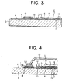
- Fig. 2 and Fig. 3 are a perspective view and a partial cross section illustrating a typical multilayer substrate to be used in embodying the present invention.
- the reference numeral 5 denotes a ceramic substrate formed of alumina or A1N, for example.
- a plurality of input and output conductor pads 6 and a plurality of relatively short connection conductor patterns 7 extending inwardly from the input and output conductor pads 6 are simultaneously formed in a thickness in the range of 1 to 20 ⁇ m by a method which comprises screen printing, drying, and firing and uses a conductive paste such as, for example Cu paste, Ag-Pt paste, Au-Pt paste, or Ag-Pd paste which exhibits satisfactory wettability to the solder and diffuses at a low speed in the solder.
- annular inorganic insulation layer 8 is deposited across over the connection conductor patterns by a method which comprises screen printing, drying, and firing and uses a crystallized glass paste.
- annular metallized layer 9 having a slightly smaller width than the inorganic insulation layer 8 is formed by printing the aforementioned conductive paste in such a manner that the underlying inorganic insulation layer will expose on both sides of the metallized layer, and drying and firing the applied conductive paste.
- a thin-film conductor pattern 10 formed in a thickness of about 1 ⁇ m using a conductive metal composed of copper as a main component and other additional metal such as, for example, Cr/Cu, Ti/Cu, Cr/Cu/Cr, Ti/Cu/Cr, Cr/Cu/Au, or Ti/Cu/Au and a polyimide layer 11 having the thickness of about 10 um are alternately superposed to produce a copper-polyimide multilayered wiring portion 12.
- This multilayered wiring portion 12 is produced as follows.
- the conductive metal composed mainly of copper as described above is deposited in the form of a thin layer by evaporating or spattering on the ceramic substrate 5 inside the annular metallized layer 9.
- This thin film is etched by photolithography to remove unnecessary portions and produce a thin-film conductor pattern 10 as the first layer.
- the thin-film conductor pattern 10 as the first layer is so formed that the edge thereof will overlie the inner edges of the connection conductor patterns.
- it is electrically connected to the input and output conductor pads 6 through the medium of the connection conductor patterns 7.
- a polyimide layer 11 is formed on thin-film conductor pattern 10 by depositing a polyimide resin solution by spin coating, drying the applied coat, and curing the coat.
- the polyimide layer 11 is etched by photolighography to form therein via holes 13 for electrically connecting the conductor patterns 10 and impart a prescribed contour thereto.
- a plurality of die pads 14 for supporting thereon such active devices as IC chips and such passive chip devices as resistors and capacitors and a plurality of outer lead bonding pads (OLB) 15 for electrically connecting the multilayered wiring portion 12 to the active devices mounted thereon through the medium of bonding wires are formed to complete copper-polyimide multilayered wiring portion 12.
- the electronic devices are generally mounted as follows. By hermetically coating the electronic devices so mounted on the multilayer substrate, the electronic apparatus contemplated by this invention is completed.
- IC chips 16 and resistors are severally joined with an adhesive agent 17 such as a conductive epoxy resin. These IC chips 16 and the corresponding OLB's 15 are electrically connected with bonding wires 18 such as, for example, Au wires or Al wires.
- bonding wires 18 such as, for example, Au wires or Al wires.
- a cap 19 made of a metal such as Kovar or Fe/Ni42 Alloy which has substantially the same thermal expansion coefficient as the ceramic is fixed with a eutectic solder 20 such as, for example the Sn/Pb 63/37 alloy.
- the air entrapped within the space enclosed with the metallic cap 19 land a accommodating therein the IC chips and other devices is displaced with an inactive gas 21 such as helium or nitrogen. Then, the cap 19 is sealed hermetically.
- input and output leads such as the clip leads and input and output pins (not shown) are fixed as with a eutectic solder.
- the multilayered wiring portion 12 on which the IC chips 16 and other electronic devices are mounted is formed of a polyimide resin possessing a very low dielectric constant as compared with the ceramic or crystallized glass, the floating capacity for distributed line patterns is small and the active devices such as the IC chips mounted on the multilayered wiring portion are enabled to operate at high speeds.
- the empty space in which the IC chips 16 and other electronic devices are disposed is hermetically sealed with the metallic cap 19 and further since the peripheral portions exposed outside the metallic cap 19 are formed of the inorganic insulation layer 8 and the ceramic substrate 5 which are inorganic materials highly impervious to moisture, the interior of the metallic cap 19 never admits moisture and the electronic apparatus is perfectly free from the dangers of migration, corrosion of wires, and formation of dew.
- the annular metallized layer 9 and the input and output conductor pads 6 are both formed by the thick-film method using conductive metals which exhibit highly satisfactory wettability to the solder and diffuse at low speed in the solder, the metallic cap 19 and the input and output leads can be fixed strongly thereon with the solder 20.
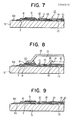
- Fig. 5 is a partially magnified cross section of another typical multilayer substrate to be used in embodying the present invention
- Fig. 6 is a partially magnified cross section of another embodiment of this invention using this distribution substrate.
- This embodiment is identical in construction with the embodiment illustrated in Figs. 2 through 4, excepting the input and output conductor pads 6 are formed by the thin-film method using copper and other conductive metal than copper such as, for example, Cr/Cu, Ti/Cu, Cr/Cu/Cr, Ti/Cu/Cr, Cr/Cu/Au, or Ti/Cu/Au instead of the thick-film method.
- Cr/Cu Ti/Cu, Cr/Cu/Cr, Ti/Cu/Cr, Cr/Cu/Au
- Ti/Cu/Au instead of the thick-film method.
- the input and output conductor pads 6a are formed on the peripheral portion of the ceramic substrate 5 by the thin-film method using the aforementioned two-component or three-component conductive metal having copper as a main component in such a manner that part of the formed pads will float up on the connection conductor patterns 7.
- the input and output conductor pads 6a are formed at the same time that the plurality of die pads 14 and the plurality of outer lead bonding pads (OLB) 15 are formed on the uppermost layer of the multilayered wiring portion 12.
- the input and output conductor pads 6a are formed of a thin film of the two- component or three-component conductive metal having copper as a main component and excelling in solderability, the input and output leads or the input and output pins can be soldered with ample strength.
- Fig. 7 is a partial cross section of yet another typical multilayer substrate to be used in this invention and Fig. 8 is a partial cross section illustrating yet another embodiment of this invention using the distribution substrate just mentioned.
- the present embodiment is identical in construction with the embodiment illustrated in Figs. 2 through 4, excepting the input and output conductor pads 6b are formed of a thin film of the two-component or three-component conductive metal having copper as a main component and excelling in solderability and a thin film of the two-component or three-component conductive metal having copper as a main component and excelling in solderability is formed on the metallized layer 9.
- the component parts of this embodiment which have equals in the embodiment illustrated in Figs. 2 through 4, therefore, will be denoted by equal reference numerals and will be omitted from the following description of the present embodiment.
- the input and output conductor pads 6b are formed by the thin-film method in such a manner as to extend from the edge of the ceramic substrate 5 to the inorganic insulation layer 8 astride the connection conductor patterns 7.
- the annular metallized layer 9 formed by the thick-film method which is excellent in the fine pattern property and the multi-layer property and deficient in the property of union with solder is perfectly coated with a thin film using a conductive metal having as its main component copper, a highly solderable substance.
- the present embodiment can afford an electronic apparatus having a metallic cap 19 fixed therein with great strength.
- Fig. 6 and Fig. 8 represent cases in which the input and output conductor pads 6a and 6b are formed solely of a thin film using the two-component or three-component conductive metal having copper as a main component.
- a plurality of input and output conductor pads 6c may be formed adjacently to the peripheral portion of the ceramic substrate 5 by the thick-film method using an Au paste, for example, in such a manner as to contact the connection conductor patterns 7 electrically and input and output conductor pads 6b one size larger than the input and output conductor pads 6c may be formed on the input and output conductor pads 6c by the thin-film method using a conductive metal having copper as a main component as illustrated in Fig. 9.
- the input and output conductor pads 6b which are formed of a thin film are fixed on the ceramic substrate 5 through the medium of the input and output conductor pads 6c formed of a thick-film conductor excelling in conductivity and abounding with adhesive strength to the ceramic substrate, the adhesive strength relative to the ceramic substrate and the soldering strength relative to the metallic cap are both improved.
Abstract
Description
- This invention relates to an electronic apparatus and more particularly to an electronic apparatus of the type which, like a hybrid IC, has electronic devices mounted on a multilayer substrate and covered with a hermetic cap.
- The desirability of the trend of electronic apparatus toward decrease of size and weight, diversification of function, increase of operational speed, and improvement of operational reliability has been finding growing recognition. In reply to this demand, hybrid IC's constructed by mounting numerous chip components such as IC chips, resistors, and capacitors on a multilayer ceramic substrate and hermetically covering these chip components with a metallic cap are finding increasing applications.
- The ceramic multilayer substrates which are used for such hybrid IC's have been heretofore produced by the green sheet method, the thick film method, or the mixed thick film-thin film method.
- In the ceramic multilayer substrates, since the insulation layers are formed of such materials of relatively large dielectric constants (ε) as ceramic (ε = 8 to 10) and crystallized glass (ε = 9 to 20), it is difficult to keep the floating capacity for wiring line patterns down to a low level. This difficulty has formed the cause for the retardation in the improvement of operational speed of the component devices mounted on the substrates.
- Recently, a copper-polyimide multilayer substrate has been developed for supporting high-speed devices. This multilayer substrate has a construction in which, as illustrated in Fig. 1, a thin-film conductor pattern 1 formed mainly of copper in a thickness of about 1 to 10 µm, generally 1 to 3 µm and a
polyimide layer 2 having the thickness of about 10 µm are alternately superposed a plurality of times on a ceramic substrate 3. It is produced as follows. - First, the thin-film conductor pattern is formed by evaporating or spattering copper land a conductive metal other than copper thereby supperposing a conductor layer on the entire surface of the ceramic substrate 3 and etching unnecessary portions by the photolithographic technique. Then, on this thin-film conductor pattern, polyimide is deposited in the form of a thin layer by spin coating and this thin layer is dried. By photolithography, via
holes 4 are formed to interconnect the upper and lower conductor patterns 1 electrically. By repeating this procedure a plurality of times, there is obtained a copper-polyimide multilayer substrate. - This copper-polyimide mutilayer substrate permits the devices mounted thereon to operate at high speeds because the polyimide resin of which the insulation layers are made has an extremely small dielectric constant (ε = 3 to 4) and further because the conductor patterns 1 are formed of a smallerconductive electric resistance than other metals.
- This copper-polyimide multilayer substrate, however, has a disadvantage that the polyimide resin used therein is hygroscopic. The hybrid IC which is produced by mounting IC chips on this substrate and hermetically sealing the IC chips with a metallic cap, therefore, suffers moisture to permeate through the
polyimide layer 2 and reach the interior of the metallic cap. - Thus, the conventional hybrid IC's using this copper-polyimide multilayer substrate have had the disadvantage that the humidity reaching the interior of the metallic cap through the
polyimide layer 2 will expose the multilayered wiring portion to the danger of forming closed-circuit failure through migration, the IC chips and bonding wires to the danger of yielding to corrosion, and the entire IC proper to the danger of establishing closed-circuit failure due to formation of dew during the course of the temperature cycling test. - A primary object of this invention, therefore, is to provide an electronic apparatus constructed that the IC chips mounted on the substrate thereof will operate at high speeds, the portion hermetically sealed with a cap will not admit moisture, and the danger of migration, the danger of wire corrosion, the danger of dew formation, and the danger of estabilishment of closed-circuit failure due to formation of dew during the course of temperature cycling test will never happen.
- Another object of this invention is to provide an electronic apparatus incorporating therein an input-output conductor pad which enables a metallic cap, input and output leads, and input and output pins to be fixed thereto with full strength.
- The electronic apparatus of this invention comprises a ceramic substrate, a multilayered wiring portion disposed at a distance from the periphery of the main surface of the ceramic substrate and produced by althernately repeating a conductor pattern formed by the thin-film method using a conductive metal and a polyimide layer, electronic devices mounted on the multilayered wiring portion and electrically connected to the conductor patterns of the multilayered wiring portion, input and output conductor pads formed on the periphery of the main surface of the ceramic substrate, connection conductor patterns formed on the main surface of the ceramic substrate astride the gap between the line patterns of the multilayered wiring portion and the input and output conductor pads, an inorganic insulation layer formed annularly on the main surface of the ceramic substrate across over at least part of the connection conductor patterns around the multilayered wiring portion, a metallized layer formed on the inorganic insulation layer, and a moistureproof cap having the edge thereof hermetically fixed by soldering on the metallized layer.
- As the ceramic substrate mentioned above, there can be used an alumina substrate or an A1N substrate, for example.
- The conductor pattern as the first layer in the multilayered wiring portion is formed, for example, by forming a conductive metal coat on the entire surface of a ceramic substrate by the thin-film method, i.e. by evaporating or spattering a conductive metal such as Cr/Cu, Ti/Cu, Cr/Cu/Cr, Ti/Cu/Ti, Cr/Cu/Au, or Ti/Cu/Au which has copper as a main component and etching the conductive metal coat in a prescribed pattern by the photolithographic method. The conductor pattern as the lowermost layer is formed in such a manner that the edges thereof will be superposed on the inner edges of the connection conductor patterns which will be described more fully later on and is electrically connected to the connection conductor patterns. The polyimide layer superposed on the thin-film conductor pattern is formed, for example, by applying a photosensitive polyimide resin in the form of a thin film by spin coating on the aforementioned conductor pattern, drying the applied film of the polyimide resin, and etching the dry film photolighographically in such a manner as to impart via holes and a visible contour thereto.
- The multilayered wiring portion is formed by alternately repeating the aforementioned thin-film conductor pattern and polyimide layer a plurality of times.
- The input and output conductor pads and the connection conductor patterns are generally formed by superposing a pasty conductive composition on the ceramic substrate by the thick-film method, i.e. by printing the pasty conductive composition in prescribed patterns by the screen printing method and drying and firing the deposited layers of the composition. As examples of the pasty conductive composition suitably used by the thick-film method, there may be cited Cu paste, Ag-Pt paste, Au-Pt paste, and Ag-Pd paste which exhibit satisfactory wettability and low diffusibility to the Sn-Pb type solder. Suitably, the thickness which the input and output conductor pads and the connection conductor patterns will assume after the firing are approximately in the range of 1 to 20 µm.
- The thick-film method described herein, has generally two process as follows.
- In the first process, a photosensitive layer is formed by applying a photosensitive emulsion on a screen having generally 325 mesh and drying the screen. Then this photosensitive layer is exposed by using a mask and developed. Thereby, this layer is partially removed. Setting the obtained screen on the substrate and printing by using a pasty conductive composition, this pasty composition is printed on the screen only to the part which the photosensitive layer is partially removed. This process can be used for forming a conductor pattern generally having the line width of about 100 µm or more and the thickness in the range of 10 to 15 µm.
- In the second process, the pasty conductive composition is printed on the substrate in the thin layer state by using the screen having generally 400 mesh. This layer of pasty conductive composition is dried and fired, thereby caused a uniformed conductor layer. Then this conductor layer is etched by the photolithographic technique. Thereby, the prescribed conductor pattern can be obtained. This process can be used for forming a fine conductor pattern generally having the line width in the range of 30 to 50 µm and the thickness in the range of 3 to 5 µm.
- Optionally, the input and output conductor pads may be formed in combination with the conductor pattern as the uppermost layer of the multilayered wiring portion, subsequently to the formation of the connecting conductor patterns by the thick-film method, in accordance with the thin-film method applying the aforementioned conductive metal composed mainly of copper in such a manner as to overlie the outer edges of the connection conductor patterns. The input and output conductor pads may be otherwise obtained by first forming the conductor metal in a prescribed shape by the thick-film method using an Au paste in such a manner as to come into contact with the outer edges of the connection conductor patterns and then coating the deposited layer of the conductor metal with a metal layer formed mainly of copper by the thin-film method.
- As the annular inorganic insulation layer to be formed across the connection conductor patterns, it is suitable to use what is produced in a thickness in the range of 10 to 40 µm by the so-called thick-film method which comprises applying an inorganic insulator paste such as crystallized glass or ceramic in a prescribed pattern on a surface by screen printing and then firing the applied layer.
- The annular metallized layer to be formed on the inorganic insulation layer is destined to function as a seal ring pattern while a hermetic cap such as the metallic cap disposed to enclose such devices as IC chips mounted on the multilayered wiring portion is fixed by fusion with a solder. It is superposed on the inorganic insulation layer by the thick-film method using either the aforementioned pasty conductive composition or a pasty conductive composition containing metal powder, metal oxide, etc. Where the annular metallized layer and the input and output conductor pads are formed by the thick-film method specifically using a pasty conductive composition which exhibits satisfactory wettability to the Sn-Pb type solder and diffuses at a low speed in this solder, there is derived the advantage that the layer and the pads so produced will increase the strength of fixation and facilitate the work of soldering when the metallic cap, input and output leads, or input and output pins are to be fixed thereon as with a solder.
- Optionally on the entire surfaces of the input and output conductor pads, the connection conductor patterns and the annular metallized layer which have been produced by the thick-film method, the aforementioned conductive metal composed mainly of copper may be applied by the thin-film method so as to coat completely the thick-film layers. The thin-film coats thus added further enhance the strength of fixation and further facilitate the work of soldering when the moistureproof cap, inlet and outlet leads, and input and output pins are to be fixed thereon as with a solder.
- The IC chips and the electronic chip components such as resistors and capacitors are mounted on the multilayered wiring portion by a suitable conventional method such as, for example, the wire bonding method or the method of electric connection using bumps and no wire.
- On the annular metallized layer, a moistureproof cap such as the metallic cap is hermetically deposited by soldering.
- In accordance with the present invention, the metallic cap can be fixed hermetically with the upper side of the annular metallized layer by soldering. Moreover, since the inorganic insulation layer completely outside the seal ring pattern is formed of ceramic or crystallized glass, there is absolutely no possibility of any humidity permeating through the inorganic insulation layer in the direction of thickness. Thus, the electronic apparatus of the present invention is perfectly free from the dangers of closed-circuit failure, corrosion, due to formation of dew and warrants highly reliable performance.
- Fig. 1 is a cross section of a copper-polyimide multilayer substrate,
- Fig. 2 and Fig. 3 are a perspective view and a partially magnified cross section illustrating a typical multilayer substrate to be used for the electronic apparatus of the present invention,
- Fig. 4 is a partially magnified cross section illustrating one embodiment of the present invention using the multilayer substrate mentioned above,
- Fig. 5 is a partially magnified cross section illustrating another typical multilayer substrate to be used in embodying the present invention,
- Fig. 6 is a partially magnified cross section illustrating another embodiment of the present invention using the multilayer substrate just mentioned,
- Fig. 7 is a partially magnified cross section illustrating yet another typical multilayer substrate to be used in embodying the present invention,
- Fig. 8 is a partially magnified cross section illustrating yet another embodiment of the present invention using the mutilayer substrate mentioned above, and
- Fig. 9 is a partial cross section illustrating still another multilayer substrate to be used in embodying the present invention.
- Now, the preferred embodiments of the present invention will be described below with reference to the accompanying drawings.
- Fig. 2 and Fig. 3 are a perspective view and a partial cross section illustrating a typical multilayer substrate to be used in embodying the present invention.
- In these diagrams, the
reference numeral 5 denotes a ceramic substrate formed of alumina or A1N, for example. On the peripheral portion of the main surface of thisceramic substrate 5, a plurality of input andoutput conductor pads 6 and a plurality of relatively shortconnection conductor patterns 7 extending inwardly from the input andoutput conductor pads 6 are simultaneously formed in a thickness in the range of 1 to 20 µm by a method which comprises screen printing, drying, and firing and uses a conductive paste such as, for example Cu paste, Ag-Pt paste, Au-Pt paste, or Ag-Pd paste which exhibits satisfactory wettability to the solder and diffuses at a low speed in the solder. - Inside the rows of these input and
output conductor pads 6, an annularinorganic insulation layer 8 is deposited across over the connection conductor patterns by a method which comprises screen printing, drying, and firing and uses a crystallized glass paste. - On this annular
inorganic insulation layer 8, anannular metallized layer 9 having a slightly smaller width than theinorganic insulation layer 8 is formed by printing the aforementioned conductive paste in such a manner that the underlying inorganic insulation layer will expose on both sides of the metallized layer, and drying and firing the applied conductive paste. - Further, inside the
annular metallized layer 9 on the surface of theceramic substrate 5, a thin-film conductor pattern 10 formed in a thickness of about 1 µm using a conductive metal composed of copper as a main component and other additional metal such as, for example, Cr/Cu, Ti/Cu, Cr/Cu/Cr, Ti/Cu/Cr, Cr/Cu/Au, or Ti/Cu/Au and apolyimide layer 11 having the thickness of about 10 um are alternately superposed to produce a copper-polyimidemultilayered wiring portion 12. - This
multilayered wiring portion 12 is produced as follows. - First, the conductive metal composed mainly of copper as described above is deposited in the form of a thin layer by evaporating or spattering on the
ceramic substrate 5 inside theannular metallized layer 9. This thin film is etched by photolithography to remove unnecessary portions and produce a thin-film conductor pattern 10 as the first layer. In this case, the thin-film conductor pattern 10 as the first layer is so formed that the edge thereof will overlie the inner edges of the connection conductor patterns. As a result, it is electrically connected to the input andoutput conductor pads 6 through the medium of theconnection conductor patterns 7. Then, apolyimide layer 11 is formed on thin-film conductor pattern 10 by depositing a polyimide resin solution by spin coating, drying the applied coat, and curing the coat. Then, thepolyimide layer 11 is etched by photolighography to form therein viaholes 13 for electrically connecting theconductor patterns 10 and impart a prescribed contour thereto. - By following the procedure described above, required numbers of the thin-
film conductor patterns 10 andpolyimide layers 11 are alternately superposed. On the thin-film conductor as the uppermost layer, a plurality ofdie pads 14 for supporting thereon such active devices as IC chips and such passive chip devices as resistors and capacitors and a plurality of outer lead bonding pads (OLB) 15 for electrically connecting themultilayered wiring portion 12 to the active devices mounted thereon through the medium of bonding wires are formed to complete copper-polyimidemultilayered wiring portion 12. - On this multilayer substrate, the electronic devices are generally mounted as follows. By hermetically coating the electronic devices so mounted on the multilayer substrate, the electronic apparatus contemplated by this invention is completed.
- To the
die pads 14 mounted on themultilayered wiring portion 12, IC chips 16 and resistors (not shown) are severally joined with anadhesive agent 17 such as a conductive epoxy resin. These IC chips 16 and the corresponding OLB's 15 are electrically connected withbonding wires 18 such as, for example, Au wires or Al wires. On theannular metallized layer 9, acap 19 made of a metal such as Kovar or Fe/Ni42 Alloy which has substantially the same thermal expansion coefficient as the ceramic is fixed with aeutectic solder 20 such as, for example the Sn/Pb 63/37 alloy. The air entrapped within the space enclosed with themetallic cap 19 land a accommodating therein the IC chips and other devices is displaced with aninactive gas 21 such as helium or nitrogen. Then, thecap 19 is sealed hermetically. - Further, on the input and
output conductor pads 6, input and output leads such as the clip leads and input and output pins (not shown) are fixed as with a eutectic solder. - In the electronic apparatus of the present invention which is constructed as described above, since the
multilayered wiring portion 12 on which the IC chips 16 and other electronic devices are mounted is formed of a polyimide resin possessing a very low dielectric constant as compared with the ceramic or crystallized glass, the floating capacity for distributed line patterns is small and the active devices such as the IC chips mounted on the multilayered wiring portion are enabled to operate at high speeds. - Since the empty space in which the IC chips 16 and other electronic devices are disposed is hermetically sealed with the
metallic cap 19 and further since the peripheral portions exposed outside themetallic cap 19 are formed of theinorganic insulation layer 8 and theceramic substrate 5 which are inorganic materials highly impervious to moisture, the interior of themetallic cap 19 never admits moisture and the electronic apparatus is perfectly free from the dangers of migration, corrosion of wires, and formation of dew. - In the present embodiment, since the
annular metallized layer 9 and the input andoutput conductor pads 6 are both formed by the thick-film method using conductive metals which exhibit highly satisfactory wettability to the solder and diffuse at low speed in the solder, themetallic cap 19 and the input and output leads can be fixed strongly thereon with thesolder 20. - Fig. 5 is a partially magnified cross section of another typical multilayer substrate to be used in embodying the present invention and Fig. 6 is a partially magnified cross section of another embodiment of this invention using this distribution substrate. This embodiment is identical in construction with the embodiment illustrated in Figs. 2 through 4, excepting the input and
output conductor pads 6 are formed by the thin-film method using copper and other conductive metal than copper such as, for example, Cr/Cu, Ti/Cu, Cr/Cu/Cr, Ti/Cu/Cr, Cr/Cu/Au, or Ti/Cu/Au instead of the thick-film method. The component parts of this embodiment which have equals in the previous embodiment illustrated in Figs. through 4, therefore, will be denoted by equal reference numerals and will be omitted from the following description of the present embodiment. In the present embodiment, the input andoutput conductor pads 6a are formed on the peripheral portion of theceramic substrate 5 by the thin-film method using the aforementioned two-component or three-component conductive metal having copper as a main component in such a manner that part of the formed pads will float up on theconnection conductor patterns 7. - The input and
output conductor pads 6a are formed at the same time that the plurality ofdie pads 14 and the plurality of outer lead bonding pads (OLB) 15 are formed on the uppermost layer of themultilayered wiring portion 12. - In the present embodiment, since the input and
output conductor pads 6a are formed of a thin film of the two- component or three-component conductive metal having copper as a main component and excelling in solderability, the input and output leads or the input and output pins can be soldered with ample strength. - Fig. 7 is a partial cross section of yet another typical multilayer substrate to be used in this invention and Fig. 8 is a partial cross section illustrating yet another embodiment of this invention using the distribution substrate just mentioned. The present embodiment is identical in construction with the embodiment illustrated in Figs. 2 through 4, excepting the input and
output conductor pads 6b are formed of a thin film of the two-component or three-component conductive metal having copper as a main component and excelling in solderability and a thin film of the two-component or three-component conductive metal having copper as a main component and excelling in solderability is formed on the metallizedlayer 9. The component parts of this embodiment which have equals in the embodiment illustrated in Figs. 2 through 4, therefore, will be denoted by equal reference numerals and will be omitted from the following description of the present embodiment. - In this embodiment, the input and
output conductor pads 6b are formed by the thin-film method in such a manner as to extend from the edge of theceramic substrate 5 to theinorganic insulation layer 8 astride theconnection conductor patterns 7. Further in this embodiment, theannular metallized layer 9 formed by the thick-film method which is excellent in the fine pattern property and the multi-layer property and deficient in the property of union with solder is perfectly coated with a thin film using a conductive metal having as its main component copper, a highly solderable substance. As compared with the embodiment illustrated in Fig. 5, therefore, the present embodiment can afford an electronic apparatus having ametallic cap 19 fixed therein with great strength. - Fig. 6 and Fig. 8 represent cases in which the input and
output conductor pads output conductor pads 6c may be formed adjacently to the peripheral portion of theceramic substrate 5 by the thick-film method using an Au paste, for example, in such a manner as to contact theconnection conductor patterns 7 electrically and input andoutput conductor pads 6b one size larger than the input andoutput conductor pads 6c may be formed on the input andoutput conductor pads 6c by the thin-film method using a conductive metal having copper as a main component as illustrated in Fig. 9. - In the electronic apparatus using the multilayer substrate of the foregoing description, since the input and
output conductor pads 6b which are formed of a thin film are fixed on theceramic substrate 5 through the medium of the input andoutput conductor pads 6c formed of a thick-film conductor excelling in conductivity and abounding with adhesive strength to the ceramic substrate, the adhesive strength relative to the ceramic substrate and the soldering strength relative to the metallic cap are both improved.
Claims (19)
a ceramic substrate (5),
a multilayered wiring portion (12) disposed at a distance from the periphery of the main surface of said ceramic substrate (5) and produced by alternately repeating a conductor pattern (10) formed by the thin-film method using a conductive metal and a polyimide layer (11),
electronic devices mounted on said multilayered wiring portion (12) and electrically connected to the conductor patterns of said multilayered wiring portion (12),
input and output conductor pads (6) formed on the periphery of the main surface of said ceramic substrate (5),
connection conductor patterns (7) formed on the main surface of said ceramic substrate (5) astride the gap between said input and output conductor pads (6) and the line patterns of said multilayered wiring portion (12),
an inorganic insulation layer (8) formed annularly on the main surface of said ceramic substrate (5) across over at least part of said connection conductor patterns (7) around said multilayered wiring portion (12),
a metallized layer (9) formed annularly on said inorganic insulation layer (8), and
a moistureproof cap (19) having the edge thereof hermetically fixed by soldering on said metallized layer (9).
a ceramic substrate (5),
a multilayered wiring portion (12) disposed at a distance from the periphery of the main surface of said ceramic substrate (5) and produced by alternately repeating a conductor pattern (10) formed by the thin-film method using a conductive metal and a polyimide layer (11),
electronic devices mounted on said multilayered wiring portion (12) and electrically connected to the conductor patterns of said multilayered wiring portion (12),
input and output conductor pads (6) formed in the peripheral portion of the main surface of said ceramic substrate (5),
connection conductor patterns (7) formed astride the gap between said input and output conductor pads (6) and the line patterns of said multilayered wiring portion (12) both by the thick-film method using a conductive composition,
an inorganic insulation layer (8) formed annularly on the main surface of said ceramic substrate (5) across over at least part of said connection conductor patterns (7) around said multilayered wiring portion (12),
a metallized layer (9) formed annularly on said inorganic insulation layer (8), and
a moistureproof cap (19) having the edge thereof hermetically fixed by soldering on said metallized layer (9).
a ceramic substrate (5),
a multilayered wiring portion (12) disposed at a distance from the periphery of the main surface of said ceramic substrate (5) and produced by alternately repeating a conductor pattern (10) formed by the thin-film method using a conductive metal and a polyimide layer (11),
electronic devices mounted on said multilayered wiring portion (12) and electrically connected to the conductor patterns of said multilayered wiring portion (12),
input and output conductor pads (6) formed on the periphery of the main surface of said ceramic substrate (5) by the thin-film method using a conductive metal,
connection conductor patterns (7) formed on the main surface of said ceramic substrate (5) astride the gap between said input and output conductor pads (6) and the line patterns of said multilayered wiring portion (12),
an inorganic insulation layer (8) formed annularly on the main surface of said ceramic substrate (5) across over at least part of said connection conductor patterns (7) around said multilayered wiring portion (12),
a metallized layer (9) formed annularly on said inorganic insulation layer (8), and
a moistureproof cap (19) having the edge thereof hermetically fixed by soldering on said metallized layer (9).
a ceramic substrate (5),
a multilayered wiring portion (12) disposed at a distance from the periphery of the main surface of said ceramic substrate (5) and produced by alternately repeating a conductor pattern (10) formed by the thin-film method using a conductive metal and a polyimide layer (11),
electronic devices mounted on said multilayered wiring portion (12) and electrically connected to the conductor patterns of said multilayered wiring portion (12),
input and output conductor pads (6) formed on the periphery of the main surface of said ceramic substrate (5) by the thin-film method using a conductive composition,
connection conductor patterns (7) formed on the main surface of said ceramic substrate (5) astride the gap between said input and output conductor pads (6) and the line patterns of said multilayered wiring portion (12),
an inorganic insulation layer (8) formed annularly on the main surface of said ceramic substrate (5) across over at least part of said connection conductor patterns (7) around said multilayered wiring portion (12),
a metallized layer (9) formed annularly on said inorganic insulation layer (8) by the thick-film method using a conductive composition,
a conductive metal pattern formed annularly on said metallized layer by the thin-film method using a conductive metal in such a manner as to cover said metallized layer, and
a moistureproof cap (19) having the edge thereof hermetically fixed by soldering on said conductive metal pattern.
a ceramic substrate (15),
a multilayered wiring portion (12) disposed at a distance from the periphery of the main surface of said ceramic substrate (5) and produced by alternately repeating a conductor pattern (10) formed by the thin-film method using a conductive metal and a polyimide layer (11),
electronic devices mounted on said multilayered wiring portion (12) and electrically connected to the conductor patterns of said multilayered wiring portion (12),
input and output conductor pads (6) formed on the peripheral portion of the main surface of said ceramic substrate (5) with a conductive coat produced by the thickfilm method using a conductive composition and a conductive coat superposed on said conductive coat by the thin-film method using a conductive metal,
connection conductor patterns (7) formed on the main surface of said ceramic substrate (5) astride the gap between said input and output conductor pads (6) and the line patterns of said multilayered wiring portion (12),
an inorganic insulation layer (8) formed annularly on the main surface of said ceramic substrate (5) across over at least part of said connection conductor patterns (7) around said multilayered wiring portion (12),
a metallized layer (9) formed annularly on said inorganic insulation layer (8),
a conductive metal pattern formed annularly on said metallized layer by the thin-film method using a conductive metal in such a manner as to cover said metallized layer, and
a moistureproof (19) cap having the edge thereof hermatically fixed by soldering on said conductive metal pattern.
Applications Claiming Priority (6)
| Application Number | Priority Date | Filing Date | Title |
|---|---|---|---|
| JP257971/86 | 1986-10-29 | ||
| JP25797186A JPS63110755A (en) | 1986-10-29 | 1986-10-29 | Wiring substrate and manufacture thereof |
| JP25916886A JPS63111697A (en) | 1986-10-30 | 1986-10-30 | Wiring board and manufacture of the same |
| JP259168/86 | 1986-10-30 | ||
| JP25916486A JPS63111696A (en) | 1986-10-30 | 1986-10-30 | Wiring board and manufacture of the same |
| JP259164/86 | 1986-10-30 |
Publications (3)
| Publication Number | Publication Date |
|---|---|
| EP0266210A2 true EP0266210A2 (en) | 1988-05-04 |
| EP0266210A3 EP0266210A3 (en) | 1989-06-07 |
| EP0266210B1 EP0266210B1 (en) | 1993-02-17 |
Family
ID=27334685
Family Applications (1)
| Application Number | Title | Priority Date | Filing Date |
|---|---|---|---|
| EP87309593A Expired - Lifetime EP0266210B1 (en) | 1986-10-29 | 1987-10-29 | Electronic apparatus comprising a ceramic substrate |
Country Status (3)
| Country | Link |
|---|---|
| US (1) | US5153709A (en) |
| EP (1) | EP0266210B1 (en) |
| DE (1) | DE3784213T2 (en) |
Cited By (14)
| Publication number | Priority date | Publication date | Assignee | Title |
|---|---|---|---|---|
| EP0398597A2 (en) * | 1989-05-19 | 1990-11-22 | AT&T Corp. | Improved hybrid package arrangement |
| FR2653595A1 (en) * | 1989-10-25 | 1991-04-26 | Valtronic France | Electronic circuit inter-connection grid |
| WO1991011025A1 (en) * | 1990-01-16 | 1991-07-25 | A.S Micro Electronics | A method for manufacturing of mineature impedance matched interconnection patterns |
| EP0484032A2 (en) * | 1990-10-29 | 1992-05-06 | Hewlett-Packard Company | Microchip with electrical element in sealed cavity |
| EP0534133A1 (en) * | 1991-09-21 | 1993-03-31 | Alcatel SEL Aktiengesellschaft | Insulating sealing device for lead-in layers of a protection housing |
| EP0547807A2 (en) * | 1991-12-16 | 1993-06-23 | General Electric Company | Packaged electronic system |
| EP0588603A2 (en) * | 1992-09-18 | 1994-03-23 | General Electric Company | Hermetically sealed packaged electronic system and method of fabrication |
| EP0660383A1 (en) * | 1993-12-16 | 1995-06-28 | AT&T Corp. | Electronic device package |
| US5532906A (en) * | 1992-09-14 | 1996-07-02 | Kabushiki Kaisha Toshiba | Wiring substrate |
| WO1997006853A1 (en) * | 1995-08-16 | 1997-02-27 | Alfred E. Mann Foundation For Scientific Research | Hermetically sealed electrical feedthrough for use with implantable electronic devices |
| US6154372A (en) * | 1993-09-02 | 2000-11-28 | Siemens Aktiengesellschaft | Multichip module for surface mounting on printed circuit boards |
| US6516808B2 (en) | 1997-09-12 | 2003-02-11 | Alfred E. Mann Foundation For Scientific Research | Hermetic feedthrough for an implantable device |
| EP1333489A2 (en) * | 2002-01-31 | 2003-08-06 | Fujitsu Hitachi Plasma Display Limited | Semiconductor chip with a protective film |
| FR3019375A1 (en) * | 2014-03-31 | 2015-10-02 | Commissariat Energie Atomique | METHOD FOR PRODUCING A HERMETIC CASE FOR ENCAPSULATING AN IMPLANTABLE DEVICE AND CORRESPONDING HOUSING |
Families Citing this family (16)
| Publication number | Priority date | Publication date | Assignee | Title |
|---|---|---|---|---|
| US5818699A (en) * | 1995-07-05 | 1998-10-06 | Kabushiki Kaisha Toshiba | Multi-chip module and production method thereof |
| EP0794616B1 (en) * | 1996-03-08 | 2003-01-29 | Matsushita Electric Industrial Co., Ltd. | An electronic part and a method of production thereof |
| US5949654A (en) * | 1996-07-03 | 1999-09-07 | Kabushiki Kaisha Toshiba | Multi-chip module, an electronic device, and production method thereof |
| EP1014443A4 (en) * | 1996-09-20 | 2001-02-07 | Tdk Corp | Passive electronic parts, ic parts, and wafer |
| US5881945A (en) * | 1997-04-30 | 1999-03-16 | International Business Machines Corporation | Multi-layer solder seal band for semiconductor substrates and process |
| US5881944A (en) * | 1997-04-30 | 1999-03-16 | International Business Machines Corporation | Multi-layer solder seal band for semiconductor substrates |
| US5821161A (en) * | 1997-05-01 | 1998-10-13 | International Business Machines Corporation | Cast metal seal for semiconductor substrates and process thereof |
| US5982038A (en) * | 1997-05-01 | 1999-11-09 | International Business Machines Corporation | Cast metal seal for semiconductor substrates |
| US6070321A (en) | 1997-07-09 | 2000-06-06 | International Business Machines Corporation | Solder disc connection |
| US6882041B1 (en) * | 2002-02-05 | 2005-04-19 | Altera Corporation | Thermally enhanced metal capped BGA package |
| US6921630B2 (en) * | 2002-10-31 | 2005-07-26 | Sandia National Laboratories | Photoresist substrate having robust adhesion |
| KR100506738B1 (en) * | 2003-11-03 | 2005-08-08 | 삼성전기주식회사 | Leak-free sealing structure of a ceramic package, leak-free ceramic package and fabrication method of the ceramic package |
| US9254532B2 (en) | 2009-12-30 | 2016-02-09 | Intel Corporation | Methods of fabricating low melting point solder reinforced sealant and structures formed thereby |
| US20130119529A1 (en) * | 2011-11-15 | 2013-05-16 | Taiwan Semiconductor Manufacturing Company, Ltd. | Semiconductor device having lid structure and method of making same |
| US20140116500A1 (en) * | 2012-10-31 | 2014-05-01 | Emcore Solar Power, Inc. | Inverted metamorphic multijunction solar cells mounted on flexible support with bifacial contacts |
| KR102377794B1 (en) * | 2015-07-06 | 2022-03-23 | 엘지전자 주식회사 | Display device using semiconductor light emitting device and method for manufacturing |
Citations (5)
| Publication number | Priority date | Publication date | Assignee | Title |
|---|---|---|---|---|
| EP0092944A1 (en) * | 1982-04-24 | 1983-11-02 | Kabushiki Kaisha Toshiba | Method for packaging electronic parts |
| EP0113282A1 (en) * | 1982-12-28 | 1984-07-11 | Thomson-Csf | Housing for an electronic component having a humidity fixing element |
| DE3304215A1 (en) * | 1983-01-20 | 1984-07-26 | LGZ Landis & Gyr Zug AG, Zug | Ceramic housing for a hybrid circuit |
| US4558171A (en) * | 1984-10-12 | 1985-12-10 | General Electric Company | Hermetic enclosure for electronic components with an optionally transparent cover and a method of making the same |
| US4560826A (en) * | 1983-12-29 | 1985-12-24 | Amp Incorporated | Hermetically sealed chip carrier |
Family Cites Families (7)
| Publication number | Priority date | Publication date | Assignee | Title |
|---|---|---|---|---|
| US3469148A (en) * | 1967-11-08 | 1969-09-23 | Gen Motors Corp | Protectively covered hybrid microcircuits |
| US3793064A (en) * | 1971-11-15 | 1974-02-19 | Du Pont | Product and process for cavity metallization of semiconductor packages |
| JPS5471572A (en) * | 1977-11-18 | 1979-06-08 | Fujitsu Ltd | Semiconductor device |
| US4417392A (en) * | 1980-05-15 | 1983-11-29 | Cts Corporation | Process of making multi-layer ceramic package |
| JPS58223678A (en) * | 1982-06-16 | 1983-12-26 | 株式会社日立製作所 | Sic sintered body with metallized layer and manufacture |
| JPS5923531A (en) * | 1982-07-30 | 1984-02-07 | Hitachi Ltd | Semiconductor device |
| US4656499A (en) * | 1982-08-05 | 1987-04-07 | Olin Corporation | Hermetically sealed semiconductor casing |
-
1987
- 1987-10-29 EP EP87309593A patent/EP0266210B1/en not_active Expired - Lifetime
- 1987-10-29 DE DE8787309593T patent/DE3784213T2/en not_active Expired - Lifetime
-
1992
- 1992-01-09 US US07/817,996 patent/US5153709A/en not_active Expired - Lifetime
Patent Citations (5)
| Publication number | Priority date | Publication date | Assignee | Title |
|---|---|---|---|---|
| EP0092944A1 (en) * | 1982-04-24 | 1983-11-02 | Kabushiki Kaisha Toshiba | Method for packaging electronic parts |
| EP0113282A1 (en) * | 1982-12-28 | 1984-07-11 | Thomson-Csf | Housing for an electronic component having a humidity fixing element |
| DE3304215A1 (en) * | 1983-01-20 | 1984-07-26 | LGZ Landis & Gyr Zug AG, Zug | Ceramic housing for a hybrid circuit |
| US4560826A (en) * | 1983-12-29 | 1985-12-24 | Amp Incorporated | Hermetically sealed chip carrier |
| US4558171A (en) * | 1984-10-12 | 1985-12-10 | General Electric Company | Hermetic enclosure for electronic components with an optionally transparent cover and a method of making the same |
Non-Patent Citations (1)
| Title |
|---|
| IEEE PROCEEDING OD THE 31ST ELECTRONIC COMPONENTS CONFERENCE, 11th-13th May 1981, Atlanta, Feorgia, pages 9-17, IEEE, New York, US; T.S. LIU et al.: "Surface treatments and bondability of copper thick film circuits" * |
Cited By (25)
| Publication number | Priority date | Publication date | Assignee | Title |
|---|---|---|---|---|
| EP0398597A2 (en) * | 1989-05-19 | 1990-11-22 | AT&T Corp. | Improved hybrid package arrangement |
| EP0398597A3 (en) * | 1989-05-19 | 1991-11-21 | AT&T Corp. | Improved hybrid package arrangement |
| FR2653595A1 (en) * | 1989-10-25 | 1991-04-26 | Valtronic France | Electronic circuit inter-connection grid |
| WO1991011025A1 (en) * | 1990-01-16 | 1991-07-25 | A.S Micro Electronics | A method for manufacturing of mineature impedance matched interconnection patterns |
| EP0484032A2 (en) * | 1990-10-29 | 1992-05-06 | Hewlett-Packard Company | Microchip with electrical element in sealed cavity |
| EP0484032A3 (en) * | 1990-10-29 | 1992-12-23 | Hewlett-Packard Company | Microchip with electrical element in sealed cavity |
| US5490628A (en) * | 1990-10-29 | 1996-02-13 | Hewlett-Packard Company | Microchip assembly with electrical element in sealed cavity |
| EP0534133A1 (en) * | 1991-09-21 | 1993-03-31 | Alcatel SEL Aktiengesellschaft | Insulating sealing device for lead-in layers of a protection housing |
| EP0547807A3 (en) * | 1991-12-16 | 1993-09-22 | General Electric Company | Packaged electronic system |
| US5315486A (en) * | 1991-12-16 | 1994-05-24 | General Electric Company | Hermetically packaged HDI electronic system |
| EP0547807A2 (en) * | 1991-12-16 | 1993-06-23 | General Electric Company | Packaged electronic system |
| US5532906A (en) * | 1992-09-14 | 1996-07-02 | Kabushiki Kaisha Toshiba | Wiring substrate |
| EP0588603A2 (en) * | 1992-09-18 | 1994-03-23 | General Electric Company | Hermetically sealed packaged electronic system and method of fabrication |
| EP0588603A3 (en) * | 1992-09-18 | 1994-10-26 | Gen Electric | Hermetically sealed packaged electronic system and method of fabrication. |
| US6154372A (en) * | 1993-09-02 | 2000-11-28 | Siemens Aktiengesellschaft | Multichip module for surface mounting on printed circuit boards |
| EP0660383A1 (en) * | 1993-12-16 | 1995-06-28 | AT&T Corp. | Electronic device package |
| US5750926A (en) * | 1995-08-16 | 1998-05-12 | Alfred E. Mann Foundation For Scientific Research | Hermetically sealed electrical feedthrough for use with implantable electronic devices |
| WO1997006853A1 (en) * | 1995-08-16 | 1997-02-27 | Alfred E. Mann Foundation For Scientific Research | Hermetically sealed electrical feedthrough for use with implantable electronic devices |
| US6516808B2 (en) | 1997-09-12 | 2003-02-11 | Alfred E. Mann Foundation For Scientific Research | Hermetic feedthrough for an implantable device |
| EP1333489A2 (en) * | 2002-01-31 | 2003-08-06 | Fujitsu Hitachi Plasma Display Limited | Semiconductor chip with a protective film |
| EP1333489A3 (en) * | 2002-01-31 | 2006-07-26 | Fujitsu Hitachi Plasma Display Limited | Semiconductor chip with a protective film |
| US7224044B2 (en) | 2002-01-31 | 2007-05-29 | Fujitsu Hitachi Plasma Display Limited | Semiconductor chip mounting substrate and flat display |
| FR3019375A1 (en) * | 2014-03-31 | 2015-10-02 | Commissariat Energie Atomique | METHOD FOR PRODUCING A HERMETIC CASE FOR ENCAPSULATING AN IMPLANTABLE DEVICE AND CORRESPONDING HOUSING |
| EP2926865A1 (en) * | 2014-03-31 | 2015-10-07 | Commissariat A L'energie Atomique Et Aux Energies Alternatives | Method for manufacturing a sealed housing for encapsulating an implantable device and corresponding housing |
| US9387336B2 (en) | 2014-03-31 | 2016-07-12 | Commissariat A L'energie Atomique Et Aux Energies Alternatives | Method for producing a hermetically sealed casing intended for encapsulating an implantable device, and corresponding casing |
Also Published As
| Publication number | Publication date |
|---|---|
| EP0266210A3 (en) | 1989-06-07 |
| US5153709A (en) | 1992-10-06 |
| DE3784213D1 (en) | 1993-03-25 |
| DE3784213T2 (en) | 1993-06-03 |
| EP0266210B1 (en) | 1993-02-17 |
Similar Documents
| Publication | Publication Date | Title |
|---|---|---|
| EP0266210B1 (en) | Electronic apparatus comprising a ceramic substrate | |
| US5383093A (en) | Hybrid integrated circuit apparatus | |
| EP0100175B1 (en) | Chip capacitor having a compliant termination | |
| US4910643A (en) | Thick film, multi-layer, ceramic interconnected circuit board | |
| CA2024784C (en) | Stackable multilayer substrate for mounting integrated circuits | |
| US4859808A (en) | Electrical conductor having unique solder dam configuration | |
| CA2412030C (en) | Perimeter anchored thick film pad | |
| US4652977A (en) | Microelectronics module | |
| US4639830A (en) | Packaged electronic device | |
| WO1997030461A1 (en) | Resistor network in ball grid array package | |
| US6414250B1 (en) | Hermetic multi-layered circuit assemblies and method of manufacture | |
| JP3404266B2 (en) | Wiring board connection structure | |
| JPS6016749B2 (en) | Packages for integrated circuits | |
| JPS63111697A (en) | Wiring board and manufacture of the same | |
| JPS59201452A (en) | Device sealing for high density tape bonding | |
| JP2003078103A (en) | Circuit board | |
| JPS63110755A (en) | Wiring substrate and manufacture thereof | |
| JPH0365033B2 (en) | ||
| JPS6364918B2 (en) | ||
| JP2670208B2 (en) | Package for storing semiconductor elements | |
| JPH04137752A (en) | Manufacture of ceramic substrate having metallized layer | |
| JPH06151618A (en) | Package for enclosing semiconductor devices | |
| JPS63261790A (en) | Hybrid integrated circuit board | |
| JPS6384096A (en) | Circuit board | |
| JPS6010798A (en) | Method of mounting circuit element |
Legal Events
| Date | Code | Title | Description |
|---|---|---|---|
| PUAI | Public reference made under article 153(3) epc to a published international application that has entered the european phase |
Free format text: ORIGINAL CODE: 0009012 |
|
| 17P | Request for examination filed |
Effective date: 19871116 |
|
| AK | Designated contracting states |
Kind code of ref document: A2 Designated state(s): DE FR GB |
|
| PUAL | Search report despatched |
Free format text: ORIGINAL CODE: 0009013 |
|
| AK | Designated contracting states |
Kind code of ref document: A3 Designated state(s): DE FR GB |
|
| RHK1 | Main classification (correction) |
Ipc: H01L 23/10 |
|
| 17Q | First examination report despatched |
Effective date: 19910829 |
|
| GRAA | (expected) grant |
Free format text: ORIGINAL CODE: 0009210 |
|
| AK | Designated contracting states |
Kind code of ref document: B1 Designated state(s): DE FR GB |
|
| REF | Corresponds to: |
Ref document number: 3784213 Country of ref document: DE Date of ref document: 19930325 |
|
| ET | Fr: translation filed | ||
| PLBE | No opposition filed within time limit |
Free format text: ORIGINAL CODE: 0009261 |
|
| STAA | Information on the status of an ep patent application or granted ep patent |
Free format text: STATUS: NO OPPOSITION FILED WITHIN TIME LIMIT |
|
| 26N | No opposition filed | ||
| REG | Reference to a national code |
Ref country code: GB Ref legal event code: 746 Effective date: 19980909 |
|
| REG | Reference to a national code |
Ref country code: FR Ref legal event code: D6 |
|
| REG | Reference to a national code |
Ref country code: GB Ref legal event code: IF02 |
|
| PGFP | Annual fee paid to national office [announced via postgrant information from national office to epo] |
Ref country code: GB Payment date: 20061025 Year of fee payment: 20 |
|
| PGFP | Annual fee paid to national office [announced via postgrant information from national office to epo] |
Ref country code: DE Payment date: 20061026 Year of fee payment: 20 |
|
| REG | Reference to a national code |
Ref country code: GB Ref legal event code: PE20 |
|
| PG25 | Lapsed in a contracting state [announced via postgrant information from national office to epo] |
Ref country code: GB Free format text: LAPSE BECAUSE OF EXPIRATION OF PROTECTION Effective date: 20071028 |
|
| PGFP | Annual fee paid to national office [announced via postgrant information from national office to epo] |
Ref country code: FR Payment date: 20061010 Year of fee payment: 20 |