EP0263944A1 - A method of squeegeeing solder paste onto and into a printed circuit board - Google Patents
A method of squeegeeing solder paste onto and into a printed circuit board Download PDFInfo
- Publication number
- EP0263944A1 EP0263944A1 EP87111959A EP87111959A EP0263944A1 EP 0263944 A1 EP0263944 A1 EP 0263944A1 EP 87111959 A EP87111959 A EP 87111959A EP 87111959 A EP87111959 A EP 87111959A EP 0263944 A1 EP0263944 A1 EP 0263944A1
- Authority
- EP
- European Patent Office
- Prior art keywords
- solder
- mask
- blade
- holes
- amount
- Prior art date
- Legal status (The legal status is an assumption and is not a legal conclusion. Google has not performed a legal analysis and makes no representation as to the accuracy of the status listed.)
- Withdrawn
Links
Images

Classifications
-
- H—ELECTRICITY
- H05—ELECTRIC TECHNIQUES NOT OTHERWISE PROVIDED FOR
- H05K—PRINTED CIRCUITS; CASINGS OR CONSTRUCTIONAL DETAILS OF ELECTRIC APPARATUS; MANUFACTURE OF ASSEMBLAGES OF ELECTRICAL COMPONENTS
- H05K3/00—Apparatus or processes for manufacturing printed circuits
- H05K3/10—Apparatus or processes for manufacturing printed circuits in which conductive material is applied to the insulating support in such a manner as to form the desired conductive pattern
- H05K3/12—Apparatus or processes for manufacturing printed circuits in which conductive material is applied to the insulating support in such a manner as to form the desired conductive pattern using thick film techniques, e.g. printing techniques to apply the conductive material or similar techniques for applying conductive paste or ink patterns
- H05K3/1216—Apparatus or processes for manufacturing printed circuits in which conductive material is applied to the insulating support in such a manner as to form the desired conductive pattern using thick film techniques, e.g. printing techniques to apply the conductive material or similar techniques for applying conductive paste or ink patterns by screen printing or stencil printing
- H05K3/1233—Methods or means for supplying the conductive material and for forcing it through the screen or stencil
-
- H—ELECTRICITY
- H05—ELECTRIC TECHNIQUES NOT OTHERWISE PROVIDED FOR
- H05K—PRINTED CIRCUITS; CASINGS OR CONSTRUCTIONAL DETAILS OF ELECTRIC APPARATUS; MANUFACTURE OF ASSEMBLAGES OF ELECTRICAL COMPONENTS
- H05K3/00—Apparatus or processes for manufacturing printed circuits
- H05K3/10—Apparatus or processes for manufacturing printed circuits in which conductive material is applied to the insulating support in such a manner as to form the desired conductive pattern
- H05K3/12—Apparatus or processes for manufacturing printed circuits in which conductive material is applied to the insulating support in such a manner as to form the desired conductive pattern using thick film techniques, e.g. printing techniques to apply the conductive material or similar techniques for applying conductive paste or ink patterns
-
- H—ELECTRICITY
- H05—ELECTRIC TECHNIQUES NOT OTHERWISE PROVIDED FOR
- H05K—PRINTED CIRCUITS; CASINGS OR CONSTRUCTIONAL DETAILS OF ELECTRIC APPARATUS; MANUFACTURE OF ASSEMBLAGES OF ELECTRICAL COMPONENTS
- H05K2201/00—Indexing scheme relating to printed circuits covered by H05K1/00
- H05K2201/09—Shape and layout
- H05K2201/09209—Shape and layout details of conductors
- H05K2201/095—Conductive through-holes or vias
- H05K2201/09572—Solder filled plated through-hole in the final product
-
- H—ELECTRICITY
- H05—ELECTRIC TECHNIQUES NOT OTHERWISE PROVIDED FOR
- H05K—PRINTED CIRCUITS; CASINGS OR CONSTRUCTIONAL DETAILS OF ELECTRIC APPARATUS; MANUFACTURE OF ASSEMBLAGES OF ELECTRICAL COMPONENTS
- H05K2203/00—Indexing scheme relating to apparatus or processes for manufacturing printed circuits covered by H05K3/00
- H05K2203/01—Tools for processing; Objects used during processing
- H05K2203/0104—Tools for processing; Objects used during processing for patterning or coating
- H05K2203/0139—Blade or squeegee, e.g. for screen printing or filling of holes
-
- H—ELECTRICITY
- H05—ELECTRIC TECHNIQUES NOT OTHERWISE PROVIDED FOR
- H05K—PRINTED CIRCUITS; CASINGS OR CONSTRUCTIONAL DETAILS OF ELECTRIC APPARATUS; MANUFACTURE OF ASSEMBLAGES OF ELECTRICAL COMPONENTS
- H05K2203/00—Indexing scheme relating to apparatus or processes for manufacturing printed circuits covered by H05K3/00
- H05K2203/16—Inspection; Monitoring; Aligning
- H05K2203/163—Monitoring a manufacturing process
Definitions
- This invention relates to a method of squeegeeing solder paste onto and into a printed circuit board having both plated through holes (PTH) and surface mount pads.
- PTH plated through holes
- solder paste is deposited through a mask or screen, that is, a metal stencil with apertures arranged in a pattern corresponding to the desired solder locations on the substrate.
- a mask or screen that is, a metal stencil with apertures arranged in a pattern corresponding to the desired solder locations on the substrate.
- the thickness of solder deposited is controlled as a function of the mask thickness, where the thicker the mask the more solder paste is deposited.
- U.S. -A- 3,735,730 discloses apparatus for applying a flowable medium to a carrier.
- the apparatus is provided with a spreading element for applying the flowable medium evenly at all points and the pressure of which upon the exposed surface and the density of the applied flowable medium can be varied continuously during the operation of the apparatus.
- solder paste deposited at each component site is critical, and the amount required in the through holes varies from that required at a surface mount land.
- the conventional method for attaching both pin in hole and surface mount components uses two solder applications. The solder paste is first applied to the surface mount sites by screen printing, then reflowed. This step is followed by a second step using wave soldering to apply solder to the pin in hole components.
- the present invention seeks to provide a single step solder application method for both surface mount and leaded through hole components.
- a method of squeegeeing solder paste onto and into a printed circuit board having lands for surface mountable components and plated through holes for leaded components, by a single sweep of a squeegee blade across a mask having apertures corresponding to the lands and through holes, the amount of solder deposited on the surface mount lands being dependent on the thickness of the mask, is characterised, according to the invention, by controlling the amount of solder deposited into the plated through holes in dependence on the hardness of the blade and the attack angle between the blade and the surface of the mask.
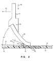
- PCB 10 is shown during a solder application process step.
- PCB 10 is provided with a plurality of plated through holes 14 in a pattern corresponding to the leads of a particular component type.
- pads 18 for surface mount components.
- Solder 20 is applied through mask 30 which has apertures (not shown) corresponding to the locations of surface mount pads 18 and PTHs 14.
- Mask 30 is preferably made of a metallic alloy such as beryllium copper having a thickness in a range of about 0.25 to 0.31 mm (10 to 12 mils).
- the screen printing mechanism includes squeegee apparatus shown schematically as including a holder 40 and resilient squeegee blade 42.
- the length of the portion 44 of the holder element 40 where blade 42 is attached is critical as it is the variation of this portion of holder 40 which provides for the variation in the attack angle for applying solder paste 20. As illustrated in Fig. 1, the short holder causes blade 42 to make an angle 48 with the surface of mask 30. Solder paste 20 rolls along in this space.
- solder paste 20 is pushed through mask 30 so that solder "bumps" 22, one of which is shown, are applied to surface mount lands 18 and solder "mushrooms" 24 are applied in the PTHs 14.
- Fig. 2 is similar to Fig 1 except that the length of a section 50, corresponding to section 44 in Fig. 1, of holder 40 is changed so that the angle made by squeegee 42 with the mask 30 is changed. As shown in Fig. 2, the long holder makes a larger angle 48 ⁇ between blade 42 and the surface of mask 30.
- solder paste 20 is distributed across and through mask 30 by squeegee blade 42.
- Various semi-rigid plastics such as vinyl, polyethylene or silicone rubber are among the materials suitable for squeegee blade 42.
- the hardness of the squeegee blade 42 is one variable for the control of the amount of solder 24 deposited in PTHs 14. It has been found that a hardness in the range of about 60 to 80 durometers is preferable.
- Holder sections 44 and 506 will hereafter be referred to as the short and long holder respectively.
- Table 1 illustrates the results of an experiment comparing the effects of varying the hardness of the squeegee blade 22 and holder 40 section length.
- Squeegee pressure exerted in the direction of arrow 56 in Fig. 1, may be adjusted between 3.6 and 5.4 kg (8-12 lbs). for optimum solder deposition on surface pads 18. It has been found that increasing squeegee pressure does not increase solder volume in PTHs 14. That solder volume has been found to be controlled by the attack angle 48 and 48 ⁇ , Figs. 1 and 2, respectively. Changing the attack angle controls the solder deposition into PTHs 14. The squeegee angle is a function of the hardness of the squeegee blade 42 and the length of the portion (44, Fig.1; 50, Fig. 2) of the squeegee holder 40. The amount of solder 20 applied to surface mount pads 18 can be maintained constant by the constant thickness mask.
- a method has been described herein wherein the amount of solder paste deposited into and onto a PCB is independently controlled, simultaneously on surface mount pads and into the PTHs. That is, the amount of paste in the PTHs may be varied to accommodate various lead diameters and printed circuit substrate thicknesses and thereby provide adequate sol der at reflow.
- the variation in PTH solder paste amount is carried out while solder paste amount deposited on the surface mount pads is held constant.
- the amount of solder paste deposited on the surface mount pads is controlled primarily by the thickness of the stencil mask 30. This is accomplished through the relative forward motion of a squeegee blade 42 in its holder 44 having a variable length dimension which creates a variably controllable relative angle between the squeegee blade and the PCB.
Abstract
In a method of squeegeeing solder paste onto and into a printed circuit board (10) having lands (18) for surface mountable components and plated through holes (14) for leaded components, by a single sweep of a squeegee blade (42) across a mask (30) having apertures corresponding to the lands and through holes, the amount of solder deposited on the surface mount lands (18) being dependent on the thickness of the mask (30), the amount of solder deposited into the plated through holes (14) is controlled in dependence on the hardness of the blade (42) and the attack angle between the blade (42) and the surface odf the mask (30).
Description
- This invention relates to a method of squeegeeing solder paste onto and into a printed circuit board having both plated through holes (PTH) and surface mount pads.
- A variety of methods are known for applying solder to printed circuitry substrates as well as various ways to control the amount of solder deposited at any given location on the substrate. Conventionally, solder paste is deposited through a mask or screen, that is, a metal stencil with apertures arranged in a pattern corresponding to the desired solder locations on the substrate. Normally, the thickness of solder deposited is controlled as a function of the mask thickness, where the thicker the mask the more solder paste is deposited.
- U.S. -A- 3,735,730 discloses apparatus for applying a flowable medium to a carrier. The apparatus is provided with a spreading element for applying the flowable medium evenly at all points and the pressure of which upon the exposed surface and the density of the applied flowable medium can be varied continuously during the operation of the apparatus.
- When it is desired to mount both leaded through hole and surface mount components on a single printed circuit board, adjustments must be made in conventional techniques for applying solder. The amount of solder paste deposited at each component site is critical, and the amount required in the through holes varies from that required at a surface mount land. The conventional method for attaching both pin in hole and surface mount components uses two solder applications. The solder paste is first applied to the surface mount sites by screen printing, then reflowed. This step is followed by a second step using wave soldering to apply solder to the pin in hole components.
- Another method for attaching leaded through hole and surface mount components to a single printed circuit board is disclosed in U.S. -A- 4,515,304 wherein the leaded through hole components are first placed on the printed circuit board. The lead ends are crimped to hold them in place while solder paste is applied, using individual applicator nozzles, to the lead ends and to solder pads for the surface mount components. Steps of inserting, crimping, turning the board and then applying solder are required. Surface mount components may then be placed on the second side of the printed circuit board and the whole reflow soldered.
- The present invention seeks to provide a single step solder application method for both surface mount and leaded through hole components.
- A method of squeegeeing solder paste onto and into a printed circuit board having lands for surface mountable components and plated through holes for leaded components, by a single sweep of a squeegee blade across a mask having apertures corresponding to the lands and through holes, the amount of solder deposited on the surface mount lands being dependent on the thickness of the mask, is characterised, according to the invention, by controlling the amount of solder deposited into the plated through holes in dependence on the hardness of the blade and the attack angle between the blade and the surface of the mask.
- We have found that varying the hardness of the squeegee blade material and a length dimension of the blade attachment mechanism, which alters the attack angle, allows control of the amount of solder applied into the PTHs. The amount of solder applied on the surface mount pads is substantially constant even while the amount applied in the PTHs can be varied.
- How the invention can be carried out will now be described by way of example, with reference to the accompanying drawings, in which:-
- Fig. 1 is a schematic cross-section of a printed circuit board (PCB) and apparatus for applying solder paste;
- Fig.2 is simila r to Fig. 1 but the dimensions of the squeegee holder have been changed; and
- Fig. 3 shows an enlarged cross-section of the PCB after solder is applied.
- In Fig. 1, a printed circuit board (PCB) 10 is shown during a solder application process step. PCB 10 is provided with a plurality of plated through
holes 14 in a pattern corresponding to the leads of a particular component type. In addition, it is provided withpads 18 for surface mount components.Solder 20 is applied throughmask 30 which has apertures (not shown) corresponding to the locations ofsurface mount pads 18 andPTHs 14.Mask 30 is preferably made of a metallic alloy such as beryllium copper having a thickness in a range of about 0.25 to 0.31 mm (10 to 12 mils). The screen printing mechanism includes squeegee apparatus shown schematically as including aholder 40 andresilient squeegee blade 42. - The length of the portion 44 of the
holder element 40 whereblade 42 is attached is critical as it is the variation of this portion ofholder 40 which provides for the variation in the attack angle for applyingsolder paste 20. As illustrated in Fig. 1, the short holder causesblade 42 to make anangle 48 with the surface ofmask 30. Solder paste 20 rolls along in this space. - As
squeegee blade 42 passes in the direction ofarrow 46,solder paste 20 is pushed throughmask 30 so that solder "bumps" 22, one of which is shown, are applied tosurface mount lands 18 and solder "mushrooms" 24 are applied in thePTHs 14. - Fig. 2 is similar to Fig 1 except that the length of a
section 50, corresponding to section 44 in Fig. 1, ofholder 40 is changed so that the angle made bysqueegee 42 with themask 30 is changed. As shown in Fig. 2, the long holder makes a larger angle 48ʹ betweenblade 42 and the surface ofmask 30. - In normal
usage solder paste 20 is distributed across and throughmask 30 bysqueegee blade 42. Various semi-rigid plastics such as vinyl, polyethylene or silicone rubber are among the materials suitable forsqueegee blade 42. The hardness of thesqueegee blade 42 is one variable for the control of the amount ofsolder 24 deposited inPTHs 14. It has been found that a hardness in the range of about 60 to 80 durometers is preferable. - Note the difference between
squeegee holder 40 section 44 in Fig. 1 and section 506 in Fig. 2. Holder sections 44 and 506 will hereafter be referred to as the short and long holder respectively. - Making these changes in
squeegee blade 42 hardness and angle allows more or less paste or solder as required to be deposited inholes 14 without any substantial change in the amount of paste or solder deposited onsurface pads 18. Table 1 illustrates the results of an experiment comparing the effects of varying the hardness of thesqueegee blade 22 and holder 40 section length.
- Squeegee pressure exerted in the direction of
arrow 56 in Fig. 1, may be adjusted between 3.6 and 5.4 kg (8-12 lbs). for optimum solder deposition onsurface pads 18. It has been found that increasing squeegee pressure does not increase solder volume inPTHs 14. That solder volume has been found to be controlled by theattack angle 48 and 48ʹ, Figs. 1 and 2, respectively. Changing the attack angle controls the solder deposition intoPTHs 14. The squeegee angle is a function of the hardness of thesqueegee blade 42 and the length of the portion (44, Fig.1; 50, Fig. 2) of thesqueegee holder 40. The amount ofsolder 20 applied tosurface mount pads 18 can be maintained constant by the constant thickness mask. - A method has been described herein wherein the amount of solder paste deposited into and onto a PCB is independently controlled, simultaneously on surface mount pads and into the PTHs. That is, the amount of paste in the PTHs may be varied to accommodate various lead diameters and printed circuit substrate thicknesses and thereby provide adequate sol der at reflow. The variation in PTH solder paste amount is carried out while solder paste amount deposited on the surface mount pads is held constant. The amount of solder paste deposited on the surface mount pads is controlled primarily by the thickness of the
stencil mask 30. This is accomplished through the relative forward motion of asqueegee blade 42 in its holder 44 having a variable length dimension which creates a variably controllable relative angle between the squeegee blade and the PCB.
Claims (4)
1. A method of squeegeeing solder paste onto and into a printed circuit board (10) having lands (18) for surface mountable components and plated through holes (14) for leaded components, by a single sweep of a squeegee blade (42) across a mask (30) having apertures corresponding to the lands and through holes, the amount of solder deposited on the surface mount lands (18) being dependent on the thickness of the mask (30), the method being characterised by controlling the amount of solder deposited into the plated through holes (14) in dependence on the hardness of the blade (42) and the attack angle between the blade (42) and the surface of the mask (30).
2. A method as claimed in Claim 1, wherein the squeegee blade has a hardness between 60 and 80 durometer.
3. A method as claimed in Claim 1 or Claim 2, further comprising determining the attack angle between the squeegee blade and the mask by adjusting the dimensions of a holder for the blade.
4. A method as claimed in any preceding Claim, wherein the attack angle may be varied in a range from about 15 degrees to about 45 degrees.
Applications Claiming Priority (2)
| Application Number | Priority Date | Filing Date | Title |
|---|---|---|---|
| US907265 | 1986-09-15 | ||
| US06/907,265 US4919970A (en) | 1986-09-15 | 1986-09-15 | Solder deposition control |
Publications (1)
| Publication Number | Publication Date |
|---|---|
| EP0263944A1 true EP0263944A1 (en) | 1988-04-20 |
Family
ID=25423792
Family Applications (1)
| Application Number | Title | Priority Date | Filing Date |
|---|---|---|---|
| EP87111959A Withdrawn EP0263944A1 (en) | 1986-09-15 | 1987-08-18 | A method of squeegeeing solder paste onto and into a printed circuit board |
Country Status (3)
| Country | Link |
|---|---|
| US (1) | US4919970A (en) |
| EP (1) | EP0263944A1 (en) |
| JP (1) | JPS6376395A (en) |
Cited By (5)
| Publication number | Priority date | Publication date | Assignee | Title |
|---|---|---|---|---|
| DE3843984A1 (en) * | 1988-12-27 | 1990-07-05 | Asea Brown Boveri | METHOD FOR SOLDERING A WIRELESS COMPONENT, AND CIRCUIT BOARD WITH SOLDERED, WIRELESS COMPONENT |
| EP0410623A1 (en) * | 1989-07-27 | 1991-01-30 | AT&T Corp. | Method and apparatus for soldering articles |
| EP0593938A1 (en) * | 1992-10-23 | 1994-04-27 | Motorola, Inc. | Method and apparatus for uniform deposition of solder paste on a pcb |
| US6020561A (en) * | 1996-03-29 | 2000-02-01 | Intel Corporation | Printed circuit substrate with solder formed on pad-on-via and pad-off-via contacts thereof |
| CN108430160A (en) * | 2018-03-06 | 2018-08-21 | 龙岩金时裕电子有限公司 | A kind of method that wiring board carries out filling holes with resin |
Families Citing this family (23)
| Publication number | Priority date | Publication date | Assignee | Title |
|---|---|---|---|---|
| JP2674092B2 (en) * | 1988-05-27 | 1997-11-05 | 松下電器産業株式会社 | Printer |
| EP0347550A3 (en) * | 1988-06-21 | 1991-08-28 | Texas Instruments Incorporated | Process for fabricating isolated vertical and super beta bipolar transistors |
| US5044306A (en) * | 1990-06-11 | 1991-09-03 | Gunter Erdmann | Solder applying mechanism |
| US5249520A (en) * | 1991-06-07 | 1993-10-05 | International Business Machines Corporation | Mask shock absorber pad |
| US5681387A (en) * | 1993-04-30 | 1997-10-28 | Jabil Circuit Company | Segmented squeegee blade |
| US5410806A (en) * | 1993-09-15 | 1995-05-02 | Lsi Logic Corporation | Method for fabricating conductive epoxy grid array semiconductors packages |
| AU1182295A (en) * | 1993-11-19 | 1995-06-06 | Cts Corporation | Metallurgically bonded polymer vias |
| JPH07263857A (en) * | 1994-03-22 | 1995-10-13 | Melco:Kk | Electronic part mounting method of printed wiring board |
| US5522929A (en) * | 1994-08-29 | 1996-06-04 | Erdmann; Gunter | Apparatus for material deposition for circuit board manufacture |
| US5669972A (en) * | 1995-04-27 | 1997-09-23 | International Business Machines Corporation | Flex tab thick film metal mask |
| US5738904A (en) * | 1995-06-30 | 1998-04-14 | Hti Engineering Inc. | Method and apparatus for variable speed material deposition |
| US5871807A (en) * | 1995-08-14 | 1999-02-16 | Micron Display Technology, Inc. | Multiple level printing in a single pass |
| JP3410639B2 (en) | 1997-07-23 | 2003-05-26 | 株式会社日立製作所 | Paste filling method, soldering method and paste printing machine |
| KR100244965B1 (en) * | 1997-08-12 | 2000-02-15 | 윤종용 | Method for manufacturing printed circuit board(PCB) and ball grid array(BGA) package |
| US6194085B1 (en) * | 1997-09-27 | 2001-02-27 | International Business Machines Corporation | Optical color tracer identifier in metal paste that bleed to greensheet |
| US6273327B1 (en) * | 1999-06-16 | 2001-08-14 | Trw Inc. | Apparatus and method for depositing solder material onto a circuit board |
| US6702592B1 (en) | 1999-12-03 | 2004-03-09 | Seagate Technology Llc | Printed circuit board assembly with secondary side rigid electrical pin to mate with compliant contact |
| JP3846554B2 (en) * | 2001-06-01 | 2006-11-15 | 日本電気株式会社 | Mask for printing, printing method, mounting structure, and manufacturing method of the mounting structure |
| JP3931600B2 (en) * | 2001-07-31 | 2007-06-20 | 株式会社デンソー | Filling method of fluid substance |
| KR101180477B1 (en) * | 2010-02-23 | 2012-09-06 | 주식회사 화진 | A steering wheel having a heating element and apparatus for attaching on it the heating element |
| US9237655B1 (en) | 2013-03-15 | 2016-01-12 | Lockheed Martin Corporation | Material deposition on circuit card assemblies |
| US9351407B1 (en) | 2015-01-08 | 2016-05-24 | Freescale Semiconductor, Inc. | Method for forming multilayer device having solder filled via connection |
| CN114851688A (en) * | 2021-01-20 | 2022-08-05 | 中兴通讯股份有限公司 | Scraper device, solder paste printing equipment and manufacturing method of printed circuit board assembly |
Citations (4)
| Publication number | Priority date | Publication date | Assignee | Title |
|---|---|---|---|---|
| US3735730A (en) * | 1969-12-22 | 1973-05-29 | Mitter & Co | Apparatus for applying a flowable medium to a carrier |
| FR2452377A1 (en) * | 1979-03-26 | 1980-10-24 | Buser Ag Maschf Fritz | Screen printing doctor blade - is preceded by further profiled section forming inflow gap and enclosing ink chamber (NL 30.9.80) |
| US4515304A (en) * | 1982-09-27 | 1985-05-07 | Northern Telecom Limited | Mounting of electronic components on printed circuit boards |
| EP0194247A2 (en) * | 1985-03-05 | 1986-09-10 | Svecia Silkscreen Maskiner AB | A screen printer adapted for providing a layer of material on the inner surface of a hole passing through a plate |
Family Cites Families (15)
| Publication number | Priority date | Publication date | Assignee | Title |
|---|---|---|---|---|
| US3226255A (en) * | 1961-10-31 | 1965-12-28 | Western Electric Co | Masking method for semiconductor |
| DE2300289C2 (en) * | 1973-01-04 | 1985-01-10 | Mitter & Co, 4815 Schloss Holte | Device for applying liquid or pasty paint for screen printing machines |
| DE2310062A1 (en) * | 1973-02-28 | 1974-08-29 | Siemens Ag | THICK-FILM CONNECTION ON CERAMIC SUBSTRATE WITH THROUGH CONTACTS BETWEEN THE CONDUCTORS ON BOTH SIDES OF THE SUBSTRATE |
| FR2296988A1 (en) * | 1974-12-31 | 1976-07-30 | Ibm France | IMPROVEMENT OF THE MANUFACTURING PROCESSES OF A CERAMIC MULTILAYER CIRCUIT MODULE |
| US4127337A (en) * | 1976-12-06 | 1978-11-28 | Ibex Inking Systems, Inc. | Business machine inking device and method of inking business machines |
| JPS55138294A (en) * | 1979-04-11 | 1980-10-28 | Matsushita Electric Ind Co Ltd | Method of forming through hole connector |
| JPS5667989A (en) * | 1979-11-09 | 1981-06-08 | Hitachi Ltd | Method of soldering circuit board |
| DE3040314A1 (en) * | 1980-10-25 | 1982-05-27 | Licentia Patent-Verwaltungs-Gmbh, 6000 Frankfurt | Adhesive bonding of elements to circuit cards - each card having metal coating covered with layer of adhesive which enters clearance holes |
| JPS5877287A (en) * | 1981-11-02 | 1983-05-10 | 松下電器産業株式会社 | Method of producing printed circuit board |
| US4459320A (en) * | 1981-12-11 | 1984-07-10 | At&T Bell Laboratories | Maskless process for applying a patterned solder mask coating |
| US4529477A (en) * | 1983-05-02 | 1985-07-16 | Kollmorgen Technologies Corporation | Process for the manufacture of printed circuit boards |
| JPS6112108U (en) * | 1984-06-25 | 1986-01-24 | 株式会社クボタ | self-driving work vehicle |
| JPS6112110U (en) * | 1984-06-26 | 1986-01-24 | 株式会社明電舎 | Unmanned vehicle standby control device |
| US4604966A (en) * | 1985-10-10 | 1986-08-12 | International Business Machine Corp. | Continuous solder paste dispenser |
| US4761881A (en) * | 1986-09-15 | 1988-08-09 | International Business Machines Corporation | Single step solder process |
-
1986
- 1986-09-15 US US06/907,265 patent/US4919970A/en not_active Expired - Lifetime
-
1987
- 1987-08-07 JP JP62196546A patent/JPS6376395A/en active Granted
- 1987-08-18 EP EP87111959A patent/EP0263944A1/en not_active Withdrawn
Patent Citations (4)
| Publication number | Priority date | Publication date | Assignee | Title |
|---|---|---|---|---|
| US3735730A (en) * | 1969-12-22 | 1973-05-29 | Mitter & Co | Apparatus for applying a flowable medium to a carrier |
| FR2452377A1 (en) * | 1979-03-26 | 1980-10-24 | Buser Ag Maschf Fritz | Screen printing doctor blade - is preceded by further profiled section forming inflow gap and enclosing ink chamber (NL 30.9.80) |
| US4515304A (en) * | 1982-09-27 | 1985-05-07 | Northern Telecom Limited | Mounting of electronic components on printed circuit boards |
| EP0194247A2 (en) * | 1985-03-05 | 1986-09-10 | Svecia Silkscreen Maskiner AB | A screen printer adapted for providing a layer of material on the inner surface of a hole passing through a plate |
Cited By (5)
| Publication number | Priority date | Publication date | Assignee | Title |
|---|---|---|---|---|
| DE3843984A1 (en) * | 1988-12-27 | 1990-07-05 | Asea Brown Boveri | METHOD FOR SOLDERING A WIRELESS COMPONENT, AND CIRCUIT BOARD WITH SOLDERED, WIRELESS COMPONENT |
| EP0410623A1 (en) * | 1989-07-27 | 1991-01-30 | AT&T Corp. | Method and apparatus for soldering articles |
| EP0593938A1 (en) * | 1992-10-23 | 1994-04-27 | Motorola, Inc. | Method and apparatus for uniform deposition of solder paste on a pcb |
| US6020561A (en) * | 1996-03-29 | 2000-02-01 | Intel Corporation | Printed circuit substrate with solder formed on pad-on-via and pad-off-via contacts thereof |
| CN108430160A (en) * | 2018-03-06 | 2018-08-21 | 龙岩金时裕电子有限公司 | A kind of method that wiring board carries out filling holes with resin |
Also Published As
| Publication number | Publication date |
|---|---|
| JPH048959B2 (en) | 1992-02-18 |
| US4919970A (en) | 1990-04-24 |
| JPS6376395A (en) | 1988-04-06 |
Similar Documents
| Publication | Publication Date | Title |
|---|---|---|
| EP0263944A1 (en) | A method of squeegeeing solder paste onto and into a printed circuit board | |
| US5740730A (en) | Apparatus for depositing solder and adhesive materials onto a printed circuit board | |
| US4953460A (en) | Method and apparatus for screen printing | |
| US5535936A (en) | Fine pitch solder formation on printed circuit board process and product | |
| US5311405A (en) | Method and apparatus for aligning and attaching a surface mount component | |
| US4836435A (en) | Component self alignment | |
| US5172852A (en) | Soldering method | |
| US5254362A (en) | Method and apparatus for deposition of solder paste on a printed wiring board | |
| US5373984A (en) | Reflow process for mixed technology on a printed wiring board | |
| GB2307446A (en) | Solder paste deposition | |
| JP2502912B2 (en) | Apparatus and method for soldering to fine pitch | |
| US5676305A (en) | Method to achieve regulated force contact in pin transfer deposition of liquidus substances | |
| EP0487782B1 (en) | Method of soldering circuit boards | |
| US5813331A (en) | Method of printing with a differential thickness stencil | |
| AU2933597A (en) | Electroformed squeegee blade for surface mount screen printing | |
| US5668699A (en) | System and method for providing uniform solder jiunt height for printed circuit boards and their assemblies | |
| US5743007A (en) | Method of mounting electronics component | |
| US7726239B2 (en) | Controlled deposition of printing material | |
| EP0245713A1 (en) | Solder pads for use on printed circuit boards | |
| US3911163A (en) | Solder coating process and apparatus | |
| DE19854036A1 (en) | Applying pasty media e.g. adhesive, solder paste, conductive glue etc. to circuit board by transmitting vibration from squeegee to pasty medium | |
| JPH01184994A (en) | Screen printer | |
| JPH02303180A (en) | Solder printing apparatus for printed circuit board | |
| JP2824106B2 (en) | Screen printing method | |
| JPH1140936A (en) | Method of forming solder bump |
Legal Events
| Date | Code | Title | Description |
|---|---|---|---|
| PUAI | Public reference made under article 153(3) epc to a published international application that has entered the european phase |
Free format text: ORIGINAL CODE: 0009012 |
|
| AK | Designated contracting states |
Kind code of ref document: A1 Designated state(s): DE FR GB |
|
| 17P | Request for examination filed |
Effective date: 19880729 |
|
| 17Q | First examination report despatched |
Effective date: 19910430 |
|
| STAA | Information on the status of an ep patent application or granted ep patent |
Free format text: STATUS: THE APPLICATION HAS BEEN WITHDRAWN |
|
| 18W | Application withdrawn |
Withdrawal date: 19921028 |
|
| RIN1 | Information on inventor provided before grant (corrected) |
Inventor name: HOEBENER, KARL GRANT Inventor name: STANKUS, JOHN JOSEPH |