EP0261712A1 - Picture display cell, method of forming an orientation layer on a substrate of the picture display cell and monomeric compounds for use in the orientation layer - Google Patents
Picture display cell, method of forming an orientation layer on a substrate of the picture display cell and monomeric compounds for use in the orientation layer Download PDFInfo
- Publication number
- EP0261712A1 EP0261712A1 EP87201642A EP87201642A EP0261712A1 EP 0261712 A1 EP0261712 A1 EP 0261712A1 EP 87201642 A EP87201642 A EP 87201642A EP 87201642 A EP87201642 A EP 87201642A EP 0261712 A1 EP0261712 A1 EP 0261712A1
- Authority
- EP
- European Patent Office
- Prior art keywords
- picture display
- display cell
- monomer
- orientation layer
- substrate
- Prior art date
- Legal status (The legal status is an assumption and is not a legal conclusion. Google has not performed a legal analysis and makes no representation as to the accuracy of the status listed.)
- Withdrawn
Links
Images

Classifications
-
- G—PHYSICS
- G03—PHOTOGRAPHY; CINEMATOGRAPHY; ANALOGOUS TECHNIQUES USING WAVES OTHER THAN OPTICAL WAVES; ELECTROGRAPHY; HOLOGRAPHY
- G03F—PHOTOMECHANICAL PRODUCTION OF TEXTURED OR PATTERNED SURFACES, e.g. FOR PRINTING, FOR PROCESSING OF SEMICONDUCTOR DEVICES; MATERIALS THEREFOR; ORIGINALS THEREFOR; APPARATUS SPECIALLY ADAPTED THEREFOR
- G03F7/00—Photomechanical, e.g. photolithographic, production of textured or patterned surfaces, e.g. printing surfaces; Materials therefor, e.g. comprising photoresists; Apparatus specially adapted therefor
- G03F7/004—Photosensitive materials
- G03F7/027—Non-macromolecular photopolymerisable compounds having carbon-to-carbon double bonds, e.g. ethylenic compounds
-
- C—CHEMISTRY; METALLURGY
- C09—DYES; PAINTS; POLISHES; NATURAL RESINS; ADHESIVES; COMPOSITIONS NOT OTHERWISE PROVIDED FOR; APPLICATIONS OF MATERIALS NOT OTHERWISE PROVIDED FOR
- C09K—MATERIALS FOR MISCELLANEOUS APPLICATIONS, NOT PROVIDED FOR ELSEWHERE
- C09K19/00—Liquid crystal materials
- C09K19/04—Liquid crystal materials characterised by the chemical structure of the liquid crystal components, e.g. by a specific unit
- C09K19/38—Polymers
-
- G—PHYSICS
- G02—OPTICS
- G02F—OPTICAL DEVICES OR ARRANGEMENTS FOR THE CONTROL OF LIGHT BY MODIFICATION OF THE OPTICAL PROPERTIES OF THE MEDIA OF THE ELEMENTS INVOLVED THEREIN; NON-LINEAR OPTICS; FREQUENCY-CHANGING OF LIGHT; OPTICAL LOGIC ELEMENTS; OPTICAL ANALOGUE/DIGITAL CONVERTERS
- G02F1/00—Devices or arrangements for the control of the intensity, colour, phase, polarisation or direction of light arriving from an independent light source, e.g. switching, gating or modulating; Non-linear optics
- G02F1/01—Devices or arrangements for the control of the intensity, colour, phase, polarisation or direction of light arriving from an independent light source, e.g. switching, gating or modulating; Non-linear optics for the control of the intensity, phase, polarisation or colour
- G02F1/13—Devices or arrangements for the control of the intensity, colour, phase, polarisation or direction of light arriving from an independent light source, e.g. switching, gating or modulating; Non-linear optics for the control of the intensity, phase, polarisation or colour based on liquid crystals, e.g. single liquid crystal display cells
- G02F1/133—Constructional arrangements; Operation of liquid crystal cells; Circuit arrangements
- G02F1/1333—Constructional arrangements; Manufacturing methods
- G02F1/1337—Surface-induced orientation of the liquid crystal molecules, e.g. by alignment layers
- G02F1/133711—Surface-induced orientation of the liquid crystal molecules, e.g. by alignment layers by organic films, e.g. polymeric films
- G02F1/133719—Surface-induced orientation of the liquid crystal molecules, e.g. by alignment layers by organic films, e.g. polymeric films with coupling agent molecules, e.g. silane
-
- G—PHYSICS
- G03—PHOTOGRAPHY; CINEMATOGRAPHY; ANALOGOUS TECHNIQUES USING WAVES OTHER THAN OPTICAL WAVES; ELECTROGRAPHY; HOLOGRAPHY
- G03F—PHOTOMECHANICAL PRODUCTION OF TEXTURED OR PATTERNED SURFACES, e.g. FOR PRINTING, FOR PROCESSING OF SEMICONDUCTOR DEVICES; MATERIALS THEREFOR; ORIGINALS THEREFOR; APPARATUS SPECIALLY ADAPTED THEREFOR
- G03F7/00—Photomechanical, e.g. photolithographic, production of textured or patterned surfaces, e.g. printing surfaces; Materials therefor, e.g. comprising photoresists; Apparatus specially adapted therefor
- G03F7/0005—Production of optical devices or components in so far as characterised by the lithographic processes or materials used therefor
- G03F7/001—Phase modulating patterns, e.g. refractive index patterns
-
- C—CHEMISTRY; METALLURGY
- C09—DYES; PAINTS; POLISHES; NATURAL RESINS; ADHESIVES; COMPOSITIONS NOT OTHERWISE PROVIDED FOR; APPLICATIONS OF MATERIALS NOT OTHERWISE PROVIDED FOR
- C09K—MATERIALS FOR MISCELLANEOUS APPLICATIONS, NOT PROVIDED FOR ELSEWHERE
- C09K2323/00—Functional layers of liquid crystal optical display excluding electroactive liquid crystal layer characterised by chemical composition
-
- G—PHYSICS
- G02—OPTICS
- G02F—OPTICAL DEVICES OR ARRANGEMENTS FOR THE CONTROL OF LIGHT BY MODIFICATION OF THE OPTICAL PROPERTIES OF THE MEDIA OF THE ELEMENTS INVOLVED THEREIN; NON-LINEAR OPTICS; FREQUENCY-CHANGING OF LIGHT; OPTICAL LOGIC ELEMENTS; OPTICAL ANALOGUE/DIGITAL CONVERTERS
- G02F1/00—Devices or arrangements for the control of the intensity, colour, phase, polarisation or direction of light arriving from an independent light source, e.g. switching, gating or modulating; Non-linear optics
- G02F1/01—Devices or arrangements for the control of the intensity, colour, phase, polarisation or direction of light arriving from an independent light source, e.g. switching, gating or modulating; Non-linear optics for the control of the intensity, phase, polarisation or colour
- G02F1/13—Devices or arrangements for the control of the intensity, colour, phase, polarisation or direction of light arriving from an independent light source, e.g. switching, gating or modulating; Non-linear optics for the control of the intensity, phase, polarisation or colour based on liquid crystals, e.g. single liquid crystal display cells
- G02F1/133—Constructional arrangements; Operation of liquid crystal cells; Circuit arrangements
- G02F1/1333—Constructional arrangements; Manufacturing methods
- G02F1/1337—Surface-induced orientation of the liquid crystal molecules, e.g. by alignment layers
- G02F1/133711—Surface-induced orientation of the liquid crystal molecules, e.g. by alignment layers by organic films, e.g. polymeric films
- G02F1/133726—Surface-induced orientation of the liquid crystal molecules, e.g. by alignment layers by organic films, e.g. polymeric films made of a mesogenic material
Definitions
- the invention relates to a picture display cell comprising as a substrate two oppositely relocated plates which are transparent to light and which on the facing sides comprise an electrode of a material which is transparent to light having hereon an orientation layer and a sealing ring between the ends of the plates, a liquid crystalline material being provided in the space between the plates and the ring.
- the invention further relates to a method of forming an orientation layer on a substrate for the picture display cell comprising an electrode and to the materials from which the orientation layer is manufactured.
- Such a picture display cell is known from United States Patent Specification 4,469,409 in which picture display cell an orientation layer is provided on a glass substrate, which orientation layer is formed from a film of a homogeneous mixture having a silanol oligomer modified with an aromatic ring which comprises a silane group and an organic polymer.
- the picture display cell of the twisted nematic type (TN-type) according to the said United States Patent Specification comprises a substrate having an orientation layer which can better withstand elevated temperatures and has an improved bonding to the "substrate than the previously used organic polymers having an imide or quinazoline ring.
- a method of providing a polymeric layer on a substrate is described in example 1 of the United States Patent Specification in which a solution of the polymer is prepared and this solution is provided on the substrate via a spinning technique.
- German Auslegeschrift 2,315,541 discloses a picture display cell in which on the substrate an orientation is provided by vapour deposition at reduced pressure. According to these vapour deposition techniques SiO x layers are provided and more information on such layers is procured by H.A. van Sprang and R.G. Aartsen in J.Appl.Phys. 56(2), July 15, 1984, pp.251-262, in which general article the method of providing, the measurements and the apparatus used are described.
- the use of such an SiO x orientation layer in a picture display cell has for its disadvantage that with these cells only a restricted range of solid angles for the orientation of the nematic liquid crystal material is available.
- German Offenlegungschrift 3,020.645 discloses a picture display cell in which a polymeric orientation layer is provided on the substrate, which polymeric orientation layer itself is liquid crystalline. When switching on or of the voltage the liquid crystalline material and the polymeric layer are both oriented at right angles to or parallel to the substrate. The orientation layer is also in the liquid cristalline phase under operating conditions.
- Japanese Patent Application Kokai No. 52-146255 discloses a picture display cell having a liquid crystalline material in which the orientation of the liquid crystalline material takes place by incorporating herein magnetic particles, for example, -Fe 2 0 3 acicular particles which are oriented by means of a magnet, after which the temperature of the glass plates is raised so that the liquid binder at the raised temperature is made to solidify. In this manner the magnetic particles are fixed and hence also the liquid crystal material.
- the presence of the acicular -Fe 2 O 3 -particles in the picture display cell has disadvantages because under the influence of said particles interferences in the light permeability can easily occur.
- the orientation layer is formed from a monomer or lower molecular compound which is first oriented in a field and is then polymerized.
- the method of forming an orientation layer on a substrate which comprises an electrode for a picture display cell is therefore characterized in that a film of a liquid crystalline monomer is provided, said monomer is oriented at a given angle in a magnetic or an electric field and is then polymerized.
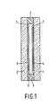
- Reference numerals 1 and 2 in the Figure denote two oppositely relocated plates which are transparent to light and which are herein after referred to as substrates and which on the facing sides comprise electrodes 4 and 5, for example, manufactured of In 2 0 3 SnOz.
- the cell is formed by placing the substrates thus formed with electrodes and orientation layer opposite to each other and sealing the aperture by means of a ring and filling the space between the substrates and the ring 3 with the liquid crystalline material 6.
- a layer of adhesive of an epoxy compound is often used as the ring 3.
- the invention resides in the fact that a liquid crystalline monomer is provided on a substrate and is oriented in an electric or magnetic field after the liquid crystalline monomer has been provided in a liquid crystalline phase and after the orientation the monomer is polymerized, possibly by exposure to actinic light.
- Another method is to heat the monomer up to a temperature above the transition nematic-isotropic and then cooling it in the field down to a temperature at which the monomer is again liquid crystalline, after which the polymerization is carried out.
- Dependent on the angle of the optical axis of the nematic groups the polymer layer induces tilted orientation in the subsequently provided liquid crystal material.
- the orientation layer there may be started from a liquid film of a crystalline (meth)-acrylate monomer.
- This monomer can be dissolved and the resulting solution can then be provided on the substrate in the form of a thin film according to a known spinning technique.
- An useful example of such an acrylate monomer is represented by the formula 4 of the formula sheet.
- liquid crystalline meth(acrylate)monomer corresponds to the formulae 2 and 3 of the formula sheet.
- the monomers of the formulae 2 and 3 are diacrylates which upon polymenication form a cross-link structure.
- the monomers of formulae 2 and 3 are novel products.
- the invention also relates to these novel products.
- the monomers of formula 2 can be prepared by a chemical process represented by reaction scheme 12 of the formula sheet.
- the monomers of formula 3 can be manufactured according to the reaction scheme 13 of the formula sheet.
- the several reactions are, as usual, performed in the presence of inert organic solvents such as ketonen, ethers or hydrocarbons.
- the reaction A and B of scheme 12 are performed in the presence of an racine, particularly a mixture (10:1) of triethyamine and 1-dimethylamino-pyridine.
- the reaction A of scheme 13 is performed in the presence of NaOH and Nal.
- the reactions C and E of - scheme 13 are performed in the presence of amine as denoted above for scheme 12.
- R 1 has the meaning disclosed hereinbefore and .... stands for an alkylene group.
- the monomer For the orientation of the mesogenic groups of the monomer in the electric or the magnetic field, the monomer must be transferred to the Iiquid crystalline phase, which is possible by raising the temperature.
- the transition from crystalline to nematic takes place at 89°C and from the nematic to the isotropic state at 98.5 °C upon heating the monomer, while upon cooling the transition from the isotropic state to the nematic state takes place at 98°C, the transition from the nematic to the smectic state at 78°C and from the smectic state to the crystalline state at 49°C.
- the orientation and the in situ polymerization preferably take place at a temperature of 89-98 * C dependent on the desired state of the orientation layer.
- the transition in a heating cycle from crystalline to smectic takes place at 17°C and from smectic to nematic at 93°C and from nematic to isotropic at 193°C. Therefore, the orientation for the monomer of formula 4 will take place at a temperature between 77 and 153°C.
- the compound of the formula 6 shows a transition from crystalline to nematic at 129°C and from nematic to isotropic at 149°C.
- the temperature at which the orientation of the monomer, notably the mesogenic group, has to be carried out may be reduced by using a mixture of monomers in which not only the orientation takes place separately but can also take place at the comparatively low temperature, possibly at ambient temperature.
- a further modification is the use of a mixture of polymer in a monomer in which the polymer may be constructed from other monomers than the monomer which is used here as a solvent.
- the polymerization of the oriented monomer preferably takes place by exposure to actinic light, notably by exposure to UV-light.
- the polymerization can be accelerated by adding to the acrylate monomers a small quantity, preferably less than 10 % by weight, of a photo initiator.
- the polymerization preferably takes place while excluding oxygen.
- the orientation of the mesogenic groups is fixed so that said anisotropy is maintained within a wide temperature range.
- the photo initiators to be used are known and an example hereof is Irgacure 651 (trademark. of CIBA-Geigy).
- a bonding layer which may consist of - methacryloxypropyl trimethoxysilane or - aminopropylsilane.
- Another embodiment which is to be preferred is to carry out the polymerization in the presence of a photo initiator which, however, is not mixed with the monomer but which photo initiator is bound to the surface so that no changes of the liquid crystalline properties of the monomer are obtained in that it is mixed with the non-liquid crystalline photo initiator and moreover the polymerization then takes place from the surface and the polymer chains are bound to the surface. In this manner it is prevented that the polymer is optionally dissolved in the liquid crystalline material 6 of the display cell.
- the photo initiator may be bound to the surface by first providing the substrate according to a known method with a layer of -aminopropylsilane, after which the substrate is immersed in a solution of a photo initiator in THF (tetrahydrofuran), for which purpose a 5 % solution of the photo initiator of formula 9 may be used. At ambient temperature the reaction takes place between - aminopropylsilane and the compound of formula 9, so that the substrate is provided with a surface film of a material which comprises both an amino group and a benzophenone group, which amino group has an accelerating effect on the photo initiation of the benzophenone group.
- THF tetrahydrofuran
- the actinic radiation is carried out with electron radiation it is not necessary to use an initiator.
- the disadvantage of this is that at the said comparatively high temperature the possibility of polymerization rather occurs so that it is to be preferred to perform the orientation at a comparatively low temperature and then to freeze the oriented monomeric groups by polymerization.
Abstract
The picture display cell comprising two transparent plates having an electrode (4, 5) with thereon an orientation layer (7) and a sealing ring (3) between the ends of the plates, a liquid crystalline (6) material being present in the space between the plates and the ring, the orientation layer being formed from a (methacrylate) monomer or a low molecular compound which is first oriented in a electric or magnetic field after having been transferred in the liquid crystalline phase by raising the temperature. Then, the polymerization of the oriented monomer takes place by exposure to actinic light (notably UV).
Description
- The invention relates to a picture display cell comprising as a substrate two oppositely relocated plates which are transparent to light and which on the facing sides comprise an electrode of a material which is transparent to light having hereon an orientation layer and a sealing ring between the ends of the plates, a liquid crystalline material being provided in the space between the plates and the ring. The invention further relates to a method of forming an orientation layer on a substrate for the picture display cell comprising an electrode and to the materials from which the orientation layer is manufactured.
- Such a picture display cell is known from United States Patent Specification 4,469,409 in which picture display cell an orientation layer is provided on a glass substrate, which orientation layer is formed from a film of a homogeneous mixture having a silanol oligomer modified with an aromatic ring which comprises a silane group and an organic polymer. The picture display cell of the twisted nematic type (TN-type) according to the said United States Patent Specification comprises a substrate having an orientation layer which can better withstand elevated temperatures and has an improved bonding to the "substrate than the previously used organic polymers having an imide or quinazoline ring. A method of providing a polymeric layer on a substrate is described in example 1 of the United States Patent Specification in which a solution of the polymer is prepared and this solution is provided on the substrate via a spinning technique.
- German Auslegeschrift 2,315,541 discloses a picture display cell in which on the substrate an orientation is provided by vapour deposition at reduced pressure. According to these vapour deposition techniques SiOx layers are provided and more information on such layers is procured by H.A. van Sprang and R.G. Aartsen in J.Appl.Phys. 56(2), July 15, 1984, pp.251-262, in which general article the method of providing, the measurements and the apparatus used are described. The use of such an SiOx orientation layer in a picture display cell, however, has for its disadvantage that with these cells only a restricted range of solid angles for the orientation of the nematic liquid crystal material is available.
- German Offenlegungschrift 3,020.645 discloses a picture display cell in which a polymeric orientation layer is provided on the substrate, which polymeric orientation layer itself is liquid crystalline. When switching on or of the voltage the liquid crystalline material and the polymeric layer are both oriented at right angles to or parallel to the substrate. The orientation layer is also in the liquid cristalline phase under operating conditions.
- Japanese Patent Application Kokai No. 52-146255 discloses a picture display cell having a liquid crystalline material in which the orientation of the liquid crystalline material takes place by incorporating herein magnetic particles, for example, -
Fe 203 acicular particles which are oriented by means of a magnet, after which the temperature of the glass plates is raised so that the liquid binder at the raised temperature is made to solidify. In this manner the magnetic particles are fixed and hence also the liquid crystal material. The presence of the acicular -Fe2O3-particles in the picture display cell, however, has disadvantages because under the influence of said particles interferences in the light permeability can easily occur. - Applicants have made further research into the orientation layer of the picture display cells and they have found that it is possible to provide a polymeric layer on the substrate, which polymeric layer can be oriented and be fixed after the orientation. As polymers could be used specific materials as described inter alia by R. Simon and H.J. Coles in Mol. Cryst. Liq. Cryst. Vol. 102 (Letters), p2. 43-48. This method yielded good results but a disadvantage was that it took some time, for example, 5 minutes to more than 1 hour, dependent on the polymer used, until the orientation layer had been oriented completely in an electric or magnetic field.
- It has now proved possible to considerably reduce said time necessary for the orientation, namely to even a few seconds, by composing a picture display cell according to the invention as described in the opening paragraph which is characterized in that the orientation layer is formed from a monomer or lower molecular compound which is first oriented in a field and is then polymerized. According to the invention, the method of forming an orientation layer on a substrate which comprises an electrode for a picture display cell is therefore characterized in that a film of a liquid crystalline monomer is provided, said monomer is oriented at a given angle in a magnetic or an electric field and is then polymerized.
- The invention will now be described in greater detail with reference to the ensuing description and the drawing, the Figure of which is cross-sectional view of a picture display cell according to the invention.
-
Reference numerals electrodes 4 and 5, for example, manufactured of In203SnOz. Anorientation layer 7 with which preferably nematicliquid crystals 6 can be oriented to provided across said electrodes. The cell is formed by placing the substrates thus formed with electrodes and orientation layer opposite to each other and sealing the aperture by means of a ring and filling the space between the substrates and thering 3 with the liquidcrystalline material 6. In practice, a layer of adhesive of an epoxy compound is often used as thering 3. - Essentially the invention resides in the fact that a liquid crystalline monomer is provided on a substrate and is oriented in an electric or magnetic field after the liquid crystalline monomer has been provided in a liquid crystalline phase and after the orientation the monomer is polymerized, possibly by exposure to actinic light. Another method is to heat the monomer up to a temperature above the transition nematic-isotropic and then cooling it in the field down to a temperature at which the monomer is again liquid crystalline, after which the polymerization is carried out. Dependent on the angle of the optical axis of the nematic groups the polymer layer induces tilted orientation in the subsequently provided liquid crystal material.
- More in particular it has been found that, in order to obtain the orientation layer, there may be started from a liquid film of a crystalline (meth)-acrylate monomer. This monomer can be dissolved and the resulting solution can then be provided on the substrate in the form of a thin film according to a known spinning technique. A suitable group of liquid crystalline acrylate monomers is represented by
formula 1 of the formula sheet, in which formula - A - is a flexible spacer, for example,
formulae - In a preferred embodiment of the picture display cell according to the invention the liquid crystalline meth(acrylate)monomer corresponds to the
formulae formulae - The monomers of
formulae formula 2 can be prepared by a chemical process represented by reaction scheme 12 of the formula sheet. The monomers offormula 3 can be manufactured according to thereaction scheme 13 of the formula sheet. The several reactions are, as usual, performed in the presence of inert organic solvents such as ketonen, ethers or hydrocarbons. The reaction A and B of scheme 12 are performed in the presence of an racine, particularly a mixture (10:1) of triethyamine and 1-dimethylamino-pyridine. The reaction A ofscheme 13 is performed in the presence of NaOH and Nal. The reactions C and E of -scheme 13 are performed in the presence of amine as denoted above for scheme 12. Inschemes 12 and 13, R1 has the meaning disclosed hereinbefore and .... stands for an alkylene group. - Useful representation of the diacrylate monomers are given by the
formulae - For the orientation of the mesogenic groups of the monomer in the electric or the magnetic field, the monomer must be transferred to the Iiquid crystalline phase, which is possible by raising the temperature. For the acrylate of formula 4, shown on the formula sheet, the transition from crystalline to nematic takes place at 89°C and from the nematic to the isotropic state at 98.5 °C upon heating the monomer, while upon cooling the transition from the isotropic state to the nematic state takes place at 98°C, the transition from the nematic to the smectic state at 78°C and from the smectic state to the crystalline state at 49°C. This means that the orientation and the in situ polymerization preferably take place at a temperature of 89-98*C dependent on the desired state of the orientation layer.
- For the acrylate monomer shown in the formula sheet by
formula 5, the transition in a heating cycle from crystalline to smectic takes place at 17°C and from smectic to nematic at 93°C and from nematic to isotropic at 193°C. Therefore, the orientation for the monomer of formula 4 will take place at a temperature between 77 and 153°C. - The compound of the
formula 6 shows a transition from crystalline to nematic at 129°C and from nematic to isotropic at 149°C. - The temperature at which the orientation of the monomer, notably the mesogenic group, has to be carried out may be reduced by using a mixture of monomers in which not only the orientation takes place separately but can also take place at the comparatively low temperature, possibly at ambient temperature. A further modification is the use of a mixture of polymer in a monomer in which the polymer may be constructed from other monomers than the monomer which is used here as a solvent. The polymerization of the oriented monomer preferably takes place by exposure to actinic light, notably by exposure to UV-light. The polymerization can be accelerated by adding to the acrylate monomers a small quantity, preferably less than 10 % by weight, of a photo initiator. The polymerization preferably takes place while excluding oxygen. As a result of the polymerization the orientation of the mesogenic groups is fixed so that said anisotropy is maintained within a wide temperature range.
- The photo initiators to be used are known and an example hereof is Irgacure 651 (trademark. of CIBA-Geigy).
- It may be advantageous not to provide the film of the monomer directly on the substrate material but first to provide said substrate material with a bonding layer which may consist of - methacryloxypropyl trimethoxysilane or - aminopropylsilane. Another embodiment which is to be preferred is to carry out the polymerization in the presence of a photo initiator which, however, is not mixed with the monomer but which photo initiator is bound to the surface so that no changes of the liquid crystalline properties of the monomer are obtained in that it is mixed with the non-liquid crystalline photo initiator and moreover the polymerization then takes place from the surface and the polymer chains are bound to the surface. In this manner it is prevented that the polymer is optionally dissolved in the liquid
crystalline material 6 of the display cell. - The photo initiator may be bound to the surface by first providing the substrate according to a known method with a layer of -aminopropylsilane, after which the substrate is immersed in a solution of a photo initiator in THF (tetrahydrofuran), for which purpose a 5 % solution of the photo initiator of
formula 9 may be used. At ambient temperature the reaction takes place between - aminopropylsilane and the compound offormula 9, so that the substrate is provided with a surface film of a material which comprises both an amino group and a benzophenone group, which amino group has an accelerating effect on the photo initiation of the benzophenone group. - If the actinic radiation is carried out with electron radiation it is not necessary to use an initiator. When the orientation of the mesogenic group in the monomer has to be carried out at a comparatively high temperature,the disadvantage of this is that at the said comparatively high temperature the possibility of polymerization rather occurs so that it is to be preferred to perform the orientation at a comparatively low temperature and then to freeze the oriented monomeric groups by polymerization.
Claims (13)
1. A picture display cell comprising as a substrate two oppositely located plates which are transparent to light and which on the facing sides comprise an electrode of a material which is transparent to light having hereon an orientation layer and a sealing ring between the ends of the plate, a liquid crystalline material being. provided in the space between the plates and the ring, characterized in that the orientation layer is formed from a monomer or low molecular compound which is first oriented in a field and is then polymerized.
2. A picture display cell as claimed in Claim 1, characterized in that the orientation layer is built up from a polymer obtained by the polymerization of oriented liquid crystalline (meth)acrylate monomers.
3. A picture display cell as claimed in Claims 1-2, characterized in that the acrylate monomers correspond to formula 1, 2 or 3 of the formula sheet, -A-being a flexible spacer, -B-being a mesogenic group, R representing a hydrogen atom or a methyl group and R2 representing an alkyl group, an aromatic group, acyane group or combinations thereof.
4. A picture display cell as claimed in Claim 3, characterized in that the acrylate monomers correspond to formula 4, 5 or 6 of the formula sheet
5. A picture display cell as claimed in Claims 1 to 4, characterized in that the orientation layer is formed from a mixture of two or more monomers which are polymerized.
6. Monomers of formula 2 or 3 of the formula sheet, in which R1 is H or CH3, and -A-is a flexible spacer, chosen from the group consisting of

wherein x = 1-15 or

7. A method of forming an orientation layer on a substrate for a picture display cell comprising an electrode, characterized in that a film of a liquid crystalline monomer is provided, said monomer is oriented in a magnetic or electric field at a given angle, and is then polymerized.
7. A method as claimed in Claim 7, characterized in that the polymerization is carried out by exposure to actinic light.
9. A method as claimed in Claims 7-8, characterized in that a photo initiator is added to a monomer in a quantity smaller than 10 % by weight calculated on the monomer.
10. A method as claimed in Claim 7-9, characterized in that monomers are used as stated in Claim 6.
11. A method as claimed in Claim 7-10, characterized in that a bonding layer is formed on the substrate before the monomeric film is provided.
12. A method as claimed in Claim 9, characterized in that the photo initiator is bonded to the surface of the substrate and is not mixed in the monomer.
13. A method as claimed in Claim 12, characterized in that the substrate is provided with a bonding agent, then with a photo initiator, after which a monomeric film is provided and after ori-. entation the polymerization of the monomeric film is carried out under the influence of UV-rays.
Applications Claiming Priority (2)
| Application Number | Priority Date | Filing Date | Title |
|---|---|---|---|
| NL8602235 | 1986-09-04 | ||
| NL8602235 | 1986-09-04 |
Publications (1)
| Publication Number | Publication Date |
|---|---|
| EP0261712A1 true EP0261712A1 (en) | 1988-03-30 |
Family
ID=19848498
Family Applications (1)
| Application Number | Title | Priority Date | Filing Date |
|---|---|---|---|
| EP87201642A Withdrawn EP0261712A1 (en) | 1986-09-04 | 1987-08-31 | Picture display cell, method of forming an orientation layer on a substrate of the picture display cell and monomeric compounds for use in the orientation layer |
Country Status (3)
| Country | Link |
|---|---|
| US (1) | US4892392A (en) |
| EP (1) | EP0261712A1 (en) |
| JP (1) | JPH083586B2 (en) |
Cited By (92)
| Publication number | Priority date | Publication date | Assignee | Title |
|---|---|---|---|---|
| EP0397263A1 (en) * | 1989-05-10 | 1990-11-14 | Koninklijke Philips Electronics N.V. | Method of manufacturing a polarisation filter, a polarisation filter thus obtained and a display having such a polarisation filter |
| EP0405713A1 (en) * | 1989-06-20 | 1991-01-02 | Edison Polymer Innovation Corporation ( Epic) | Polymerization of liquid crystalline monomers |
| EP0445629A2 (en) | 1990-03-07 | 1991-09-11 | Hercules Incorporated | Process of preparing liquid crystal compositions containing multiple oriented mesogens |
| EP0451905A1 (en) * | 1990-04-06 | 1991-10-16 | Koninklijke Philips Electronics N.V. | Liquid crystalline material and display cell containing said material |
| EP0331233A3 (en) * | 1988-02-29 | 1991-10-30 | Koninklijke Philips Electronics N.V. | Method of manufacturing a laminated element and the element thus obtained |
| EP0476543A2 (en) * | 1990-09-17 | 1992-03-25 | Matsushita Electric Industrial Co., Ltd. | Liquid crystal alignment film and method of manufacturing the same |
| US5256456A (en) * | 1990-09-17 | 1993-10-26 | Matsushita Electric Industrial Co., Ltd. | Liquid crystal alignment film and method of manufacturing the same |
| EP0601895A1 (en) * | 1992-12-11 | 1994-06-15 | Sharp Kabushiki Kaisha | Method for forming an orientation film |
| US5359253A (en) * | 1992-03-27 | 1994-10-25 | U.S. Philips Corporation | Piezoelectric material comprising a polymer network |
| WO1995022586A1 (en) * | 1994-02-19 | 1995-08-24 | Basf Aktiengesellschaft | New polymerisable liquid crystal compounds |
| WO1995024455A1 (en) * | 1994-03-11 | 1995-09-14 | Basf Aktiengesellschaft | Novel polymerizable liquid-crystalline compounds |
| WO1996024647A1 (en) * | 1995-02-06 | 1996-08-15 | Merck Patent Gmbh | Direactive mesogenic compounds and intermediates |
| WO1997004349A1 (en) * | 1995-07-21 | 1997-02-06 | The Secretary Of State For Defence | Liquid crystal polymer devices and materials |
| GB2317965A (en) * | 1995-07-21 | 1998-04-08 | Secr Defence | Liquid crystal polymer devices and materials |
| GB2330213A (en) * | 1997-10-08 | 1999-04-14 | Secr Defence | Twisted Nematic Liquid crystal device |
| GB2330214A (en) * | 1997-10-08 | 1999-04-14 | Secr Defence | Bistable nematic liquid crystal device |
| GB2331591A (en) * | 1997-11-21 | 1999-05-26 | Lg Electronics Inc | Alignment layer comprising pyranose or furanose polymer |
| EP0962460A1 (en) * | 1997-07-31 | 1999-12-08 | Matsushita Electric Industrial Co., Ltd. | Chemisorptive substance, aligned liquid-crystal film and liquid-crystal display element both made by using the same, and processes for producing these |
| US6099751A (en) * | 1996-03-21 | 2000-08-08 | Basf Aktiengesellschaft | Chiral compounds |
| US6191836B1 (en) | 1996-11-07 | 2001-02-20 | Lg Philips Lcd, Co., Ltd. | Method for fabricating a liquid crystal cell |
| EP1081207A1 (en) * | 1999-08-31 | 2001-03-07 | Canon Kabushiki Kaisha | Single-crystalline film and process for production thereof |
| US6226066B1 (en) | 1996-01-09 | 2001-05-01 | Lg. Philips Lcd Co., Ltd. | Method for controlling pretilt angle direction in a liquid crystal cell |
| US6292296B1 (en) | 1997-05-28 | 2001-09-18 | Lg. Philips Lcd Co., Ltd. | Large scale polarizer and polarizer system employing it |
| US6383579B1 (en) | 1999-04-21 | 2002-05-07 | Lg. Philips Lcd Co., Ltd. | Liquid crystal display device |
| US6479218B1 (en) | 1999-10-14 | 2002-11-12 | Lg Philips Lcd Co., Ltd | Method for manufacturing multi-domain liquid crystal cell |
| EP1342770A1 (en) * | 2002-03-04 | 2003-09-10 | Fuji Photo Film Co., Ltd. | Polymerizable liquid crystal compound, liquid crystal polymer and applications thereof |
| US6676857B2 (en) | 2001-07-25 | 2004-01-13 | Merck Patent Gesellschaft Mit | Mono-, oligo- and poly-4-fluorothiophenes and their use as charge transport materials |
| US6695978B2 (en) | 2001-09-29 | 2004-02-24 | Merck Patent Gesellschaft Mit Beschraenkter Haftung | Mono-, oligo- and polymers of benzo[b]thiophene and 2,2′-bisbenzo[b]thiophene and their use as charge transport materials |
| EP1431050A2 (en) | 2002-12-19 | 2004-06-23 | MERCK PATENT GmbH | Process for laser marking of a liquid crystal film |
| US6764724B1 (en) | 1999-03-25 | 2004-07-20 | Lg.Philips Lcd Co., Ltd. | Alignment layer for a liquid crystal display device |
| US6770335B2 (en) | 2000-10-28 | 2004-08-03 | Lg.Philips Lcd Co., Ltd. | Photoalignment materials and liquid crystal display device and method for fabricating the same with said materials |
| US6793987B2 (en) | 2000-10-28 | 2004-09-21 | Lg.Philips Lcd Co., Ltd. | Photoalignment materials and liquid crystal display fabricated with such photoalignment materials |
| US6806374B2 (en) | 2001-07-25 | 2004-10-19 | Merck Patent Gmbh | Mono-, oligo- and poly-3-(1,1-difluoroalkyl)thiophenes and their use as charge transport materials |
| US6805922B2 (en) | 2001-08-17 | 2004-10-19 | Merck Patent Gmbh | Mono-, oligo-and polyalkylidenefluorenes and their use as charge transport materials |
| US6824706B2 (en) | 2001-07-25 | 2004-11-30 | Merck Patent Gesellschaft Mit Beschrank Haftung | Mono-, Oligo- and poly-difluorovinyl-(hetero)arylenes, their synthesis and their use as charge transport materials |
| US6863841B2 (en) | 2001-12-13 | 2005-03-08 | Merck Patent Gmbh | Oxadiazole derivative and its use as charge transport and light emitting material |
| US6913710B2 (en) | 2002-04-24 | 2005-07-05 | Merck Patent Gmbh | Reactive mesogenic benzodithiophenes |
| US6924861B2 (en) | 2002-02-06 | 2005-08-02 | Merck Patent Gmbh | Birefringement film containing liquid crystal material having multi domains with splayed structure |
| US6958797B2 (en) | 2002-07-23 | 2005-10-25 | Nitto Denko Corporation | Optical film having low chromaticity variation and quarter wavelength plate, and liquid crystal display using the same |
| US7046443B2 (en) | 2002-07-24 | 2006-05-16 | Nitto Denko Corporation | Anisotropic light scattering element, anisotropic light scattering polarizing plate using the same, and image display device using the same |
| US7061679B1 (en) | 1998-05-27 | 2006-06-13 | Lg. Philips Lcd Co., Ltd. | Light irradiating device |
| US7081282B2 (en) | 2001-07-02 | 2006-07-25 | Merck Patent Gmbh | Optically variable marking |
| US7083834B2 (en) | 2002-02-13 | 2006-08-01 | Merck Patent Gmbh | Method of preparing an anisotropic polymer film on a substrate with a structured surface |
| EP1690918A2 (en) | 1998-10-20 | 2006-08-16 | Asahi Glass Company Ltd. | Liquid crystal optical element and method for its production |
| EP1701205A3 (en) * | 2005-03-07 | 2006-09-20 | L.G. Philips LCD Co., Ltd. | Method of forming alignment layer for liquid crystal display and liquid crystal display fabricated using the same |
| US7396486B2 (en) | 2002-11-07 | 2008-07-08 | Wacker Chemie Ag | Polymerizable mixtures |
| EP1093599B1 (en) * | 1998-07-08 | 2008-07-30 | Ecsibeo Ppf1 Ab | Liquid crystal device with dynamic alignment layer |
| DE112006002690T5 (en) | 2005-11-24 | 2008-10-23 | Merck Patent Gmbh | Regioregular polyselenophene |
| US7443585B2 (en) | 2002-04-23 | 2008-10-28 | Nitto Denko Corporation | Polarizer, polarization light source and image display unit using them |
| EP2033707A1 (en) | 2007-09-07 | 2009-03-11 | MERCK PATENT GmbH | Method for manufacturing a homogenous fluid mixture |
| EP2065361A2 (en) | 2007-11-30 | 2009-06-03 | Merck Patent GmbH | Polymerisable compounds |
| US7557883B2 (en) | 2006-07-12 | 2009-07-07 | Nitto Denko Corporation | Polarizing plate with optical compensation layer, method of producing the same, and liquid crystal panel, liquid crystal display, and image display including the same |
| EP2098584A1 (en) | 2008-03-05 | 2009-09-09 | Merck Patent GmbH | Liquid-crystalline medium and liquid-crystal display having high twist |
| EP2209027A1 (en) | 2002-02-13 | 2010-07-21 | MERCK PATENT GmbH | Security marking comprising an anisotropic polymer film on a substrate with a structured surface |
| EP2218764A1 (en) | 2009-02-13 | 2010-08-18 | Merck Patent GmbH | Chiral reactive mesogen mixture |
| WO2010108593A1 (en) | 2009-03-26 | 2010-09-30 | Merck Patent Gmbh | Process of preparing an anisotropic multilayer using particle beam alignment |
| US7879256B2 (en) | 2006-03-31 | 2011-02-01 | E. I. Du Pont De Nemours And Company | Liquid crystal compositions, polymer networks derived therefrom and process for making the same |
| US7914700B2 (en) | 2006-03-31 | 2011-03-29 | E. I. Du Pont De Nemours And Company | Liquid crystal compositions and polymer networks derived therefrom |
| EP2309318A1 (en) | 2008-02-29 | 2011-04-13 | Merck Patent GmbH | Alignment film for liquid crystals optainable by direct particle beam deposition |
| EP2307924A1 (en) * | 2008-07-14 | 2011-04-13 | Lensvector Inc. | Liquid crystal lens using surface programming |
| WO2011050896A1 (en) | 2009-10-30 | 2011-05-05 | Merck Patent Gmbh | Polymerisable lc material and polymer film with negative optical dispersion |
| EP2320268A1 (en) | 2009-10-26 | 2011-05-11 | Merck Patent GmbH | Alignment layer for planar alignment of a polymerizable liquid crystalline or mesogenic material |
| WO2011078055A1 (en) | 2009-12-24 | 2011-06-30 | 日東電工株式会社 | Process for production of broad-band cholesteric liquid crystal film |
| US7988881B2 (en) | 2008-09-30 | 2011-08-02 | E. I. Du Pont De Nemours And Company | Multilayer laminates comprising chiral nematic liquid crystals |
| WO2011120620A1 (en) | 2010-03-30 | 2011-10-06 | Merck Patent Gmbh | Method for producing multicoloured coatings |
| EP2399972A2 (en) | 2010-06-25 | 2011-12-28 | Merck Patent GmbH | Liquid-crystalline medium and liquid-crystal display having high twist |
| US8137582B2 (en) | 2007-08-15 | 2012-03-20 | E. I. Du Pont De Nemours And Company | Alkaloid monomers, liquid crystal compositions and polymer networks derived therefrom |
| WO2012152409A1 (en) | 2011-05-09 | 2012-11-15 | Merck Patent Gmbh | Reactive mesogen based polymer particles |
| US8388860B2 (en) | 2007-08-15 | 2013-03-05 | E I Du Pont De Nemours And Company | Chiral compounds, liquid crystal compositions and polymer networks derived therefrom |
| US8542333B2 (en) | 2008-07-14 | 2013-09-24 | Universite Laval | Liquid crystal cell alignment surface programming method and liquid cell light modulator devices made thereof |
| DE102012011464A1 (en) | 2012-06-12 | 2013-12-12 | Merck Patent Gmbh | Method for producing three-dimensional patterns in liquid-crystalline coatings |
| WO2014000846A1 (en) | 2012-06-26 | 2014-01-03 | dedeMERCK PATENT GMBH | Method of preparing a birefringent polymer film |
| WO2015058832A1 (en) | 2013-10-21 | 2015-04-30 | Merck Patent Gmbh | Method of preparing a birefringent polymer film |
| DE102013018094A1 (en) | 2013-12-03 | 2015-06-03 | Merck Patent Gmbh | Mixing device and its use |
| DE102013020400A1 (en) | 2013-12-10 | 2015-06-11 | Merck Patent Gmbh | cleaning device |
| DE102013020638A1 (en) | 2013-12-16 | 2015-06-18 | Merck Patent Gmbh | Filling device and its use for filling a fluid |
| DE102013021279A1 (en) | 2013-12-18 | 2015-06-18 | Merck Patent Gmbh | Process for cleaning a liquid crystal mixture |
| WO2016070952A1 (en) | 2014-11-06 | 2016-05-12 | Merck Patent Gmbh | Light modulation element |
| WO2016096076A1 (en) | 2014-12-19 | 2016-06-23 | Merck Patent Gmbh | Light modulation element |
| WO2016116123A1 (en) | 2015-01-23 | 2016-07-28 | Merck Patent Gmbh | Light modulation element |
| WO2016116254A1 (en) | 2015-01-23 | 2016-07-28 | Merck Patent Gmbh | Light modulation element |
| WO2017001041A1 (en) | 2015-07-02 | 2017-01-05 | Merck Patent Gmbh | Process of preparing a light modulation element |
| WO2017001043A1 (en) | 2015-07-02 | 2017-01-05 | Merck Patent Gmbh | Process of preparing a light modulation element |
| WO2017059942A1 (en) | 2015-10-06 | 2017-04-13 | Merck Patent Gmbh | Chiral compounds |
| WO2017198586A1 (en) | 2016-05-17 | 2017-11-23 | Merck Patent Gmbh | Light modulation element |
| WO2018042026A1 (en) | 2016-09-05 | 2018-03-08 | Merck Patent Gmbh | Uv curable adhesion promoters based on functionalised polyvinyl alcohols |
| WO2018073459A2 (en) | 2017-03-28 | 2018-04-26 | Merck Patent Gmbh | Liquid crystal device |
| WO2018099883A1 (en) | 2016-12-01 | 2018-06-07 | Merck Patent Gmbh | Polymerisable lc medium and polymer film with flat optical dispersion |
| WO2018192896A1 (en) | 2017-04-20 | 2018-10-25 | Merck Patent Gmbh | Light modulation element |
| WO2019121368A1 (en) | 2017-12-18 | 2019-06-27 | Merck Patent Gmbh | Liquid crystal medium and liquid crystal device |
| DE10257711B4 (en) | 2001-12-27 | 2019-09-26 | Merck Patent Gmbh | Polymerizable monocyclic compounds containing liquid crystal mixtures |
| WO2023032675A1 (en) | 2021-09-01 | 2023-03-09 | 日東電工株式会社 | Polymer dispersion type liquid crystal film, and method for producing polymer dispersion type liquid crystal film |
Families Citing this family (24)
| Publication number | Priority date | Publication date | Assignee | Title |
|---|---|---|---|---|
| US5178710A (en) * | 1988-11-02 | 1993-01-12 | U.S. Philips Corporation | Bonding using a difunctional liquid crystalline monomer adhesive under an applied force field |
| US5247379A (en) * | 1989-02-16 | 1993-09-21 | S. T. Lagerwall S.A.R.L. | Chiral nematic liquid crystal device with linear electroclinic effect |
| US5130833A (en) * | 1989-09-01 | 1992-07-14 | Semiconductor Energy Laboratory Co., Ltd. | Liquid crystal device and manufacturing method therefor |
| WO1991010149A1 (en) * | 1989-12-26 | 1991-07-11 | Allied-Signal Inc. | Method for forming optically active waveguides |
| EP0506175B1 (en) * | 1991-03-26 | 1996-12-04 | Koninklijke Philips Electronics N.V. | Liquid crystal display device comprising an orientation layer |
| US5438421A (en) * | 1991-04-24 | 1995-08-01 | Alps Electric Co., Ltd. | Orientation film of liquid crystal having bilaterally asymmetric ridges separated by grooves |
| JPH06337416A (en) * | 1993-04-02 | 1994-12-06 | Alps Electric Co Ltd | Oriented film for liquid crystal element and manufacture thereof |
| EP0659865B1 (en) * | 1993-12-24 | 1999-06-16 | Dainippon Ink And Chemicals, Inc. | Polymerizable liquid crystal composition and optically anisotropic film comprising the same |
| WO1996009567A1 (en) * | 1994-09-20 | 1996-03-28 | Philips Electronics N.V. | Manufacture of a substrate having a modified orientation layer and of a liquid crystalline display device comprising such a substrate |
| JP3195172B2 (en) * | 1994-09-21 | 2001-08-06 | アルプス電気株式会社 | Liquid crystal display device and method of manufacturing the same |
| US5846452A (en) * | 1995-04-06 | 1998-12-08 | Alliant Techsystems Inc. | Liquid crystal optical storage medium with gray scale |
| US5965081A (en) * | 1996-05-16 | 1999-10-12 | The Coca-Cola Company | Method of making side-gated preforms for use in blow molding plastic bottles |
| US5851471A (en) * | 1996-05-16 | 1998-12-22 | The Coca-Cola Company | Method for injection molding a multi-layer preform for use in blow molding a plastic bottle |
| DE19781752T1 (en) * | 1996-07-01 | 1999-09-02 | Merck Patent Gmbh | Chiral dopants |
| US5707691A (en) * | 1996-08-27 | 1998-01-13 | The Coca-Cola Company | Coating hollow containers by in-situ polymerization of monomers in bi-axially orientated form |
| KR100208475B1 (en) * | 1996-09-12 | 1999-07-15 | 박원훈 | Method for lc alignment layer with magnetic field process |
| TW472081B (en) * | 1996-09-17 | 2002-01-11 | Merck Patent Gmbh | Optical retardation film |
| KR20030041986A (en) * | 2001-07-10 | 2003-05-27 | 코닌클리케 필립스 일렉트로닉스 엔.브이. | Anisotropic composite comprising a mixture of a polymeric network and inorganic material |
| WO2005008324A1 (en) * | 2003-07-18 | 2005-01-27 | Koninklijke Philips Electronics N.V. | Liquid crystal display device comprising an anchoring layer |
| US7390540B2 (en) * | 2004-07-21 | 2008-06-24 | Hewlett-Packard Development Company, L.P. | Method for preparation of anisotropic materials |
| KR100949500B1 (en) | 2005-02-07 | 2010-03-24 | 엘지디스플레이 주식회사 | Method and Apparatus of forming an alignment layer for liquid crystal display device |
| KR100971384B1 (en) * | 2005-02-07 | 2010-07-21 | 엘지디스플레이 주식회사 | Method and Apparatus of forming an alignment layer for liquid crystal display device |
| KR101315198B1 (en) * | 2005-09-15 | 2013-10-07 | 가부시키가이샤 한도오따이 에네루기 켄큐쇼 | Manufacturing method of liquid crystal display device |
| CN108681158B (en) * | 2018-05-21 | 2021-12-03 | 南京京东方显示技术有限公司 | Self-alignment display device and alignment method thereof |
Citations (3)
| Publication number | Priority date | Publication date | Assignee | Title |
|---|---|---|---|---|
| DE3027571A1 (en) * | 1980-07-21 | 1982-02-18 | Siemens AG, 1000 Berlin und 8000 München | Liq. crystal display with orientation layer of polymer - forming solidified mesophase contg. aligned dichroitic dyestuff giving linear polarisation |
| EP0137679A1 (en) * | 1983-08-24 | 1985-04-17 | University Patents, Inc. | Diacetylenes having liquid crystal phases |
| EP0184482A1 (en) * | 1984-11-13 | 1986-06-11 | Thomson-Csf | Thermotropical polymers with chiral lateral chains, and process for their preparation |
Family Cites Families (18)
| Publication number | Priority date | Publication date | Assignee | Title |
|---|---|---|---|---|
| FR2248529B1 (en) * | 1973-10-19 | 1978-02-17 | Thomson Csf | |
| US4038441A (en) * | 1973-12-23 | 1977-07-26 | Thomson-Csf | Method of manufacturing a liquid crystal device with plane alignment |
| US4022934A (en) * | 1975-04-21 | 1977-05-10 | Hughes Aircraft Company | Means for inducing perpendicular alignment of a nematic liquid crystal on a coated substrate |
| DE2831909A1 (en) * | 1978-07-20 | 1980-02-07 | Basf Ag | LIQUID CRYSTALLINE POLYMER PHASE WITH CHOLESTERIC STRUCTURE, METHOD FOR THE PRODUCTION THEREOF AND THEIR USE |
| US4561725A (en) * | 1983-02-09 | 1985-12-31 | Canon Kabushiki Kaisha | Electro-optical device having homogeneous alignment layer hardened with cross-linking agents |
| JPS60156043A (en) * | 1984-01-23 | 1985-08-16 | Canon Inc | Liquid crystal element |
| JPS60165183A (en) * | 1984-02-06 | 1985-08-28 | Canon Inc | Image pickup element of image pickup device |
| JPS6145224A (en) * | 1984-08-10 | 1986-03-05 | Alps Electric Co Ltd | Manufacture of liquid-crystal display element |
| FR2577690B1 (en) * | 1985-02-21 | 1989-02-17 | Centre Nat Rech Scient | SURPLATINUM FOR THERMODYNAMIC STUDIES UNDER MICROSCOPE |
| US4643528A (en) * | 1985-03-18 | 1987-02-17 | Manchester R & D Partnership | Encapsulated liquid crystal and filler material |
| US4683327A (en) * | 1985-06-24 | 1987-07-28 | Celanese Corporation | Anisotropic heat-curable acrylic terminated monomers |
| EP0219336B1 (en) * | 1985-10-14 | 1993-07-21 | Hitachi Chemical Co., Ltd. | Liquid crystal orientation controlling film and liquid crystal device using the same |
| JPS62135338A (en) * | 1985-12-09 | 1987-06-18 | Diafoil Co Ltd | Monoaxially high-orientated film of polyethylene-naphthalate for liquid crystal panel substrate |
| GB2185487B (en) * | 1986-01-16 | 1990-06-06 | Gen Electric Plc | Electro-optical material |
| US4820026A (en) * | 1986-03-20 | 1989-04-11 | Canon Kabushiki Kaisha | Ferroelectric liquid crystal device with modified polyvinyl alcohol alignment film |
| JPS62245218A (en) * | 1986-04-18 | 1987-10-26 | Seiko Epson Corp | Production of liquid crystal display device |
| JPH06100755B2 (en) * | 1986-06-18 | 1994-12-12 | 日産化学工業株式会社 | Alignment treatment agent for liquid crystal cells |
| US4767191A (en) * | 1986-11-14 | 1988-08-30 | U.S. Philips Corporation | Display cell |
-
1987
- 1987-08-31 EP EP87201642A patent/EP0261712A1/en not_active Withdrawn
- 1987-09-04 JP JP62220529A patent/JPH083586B2/en not_active Expired - Fee Related
-
1988
- 1988-11-02 US US07/267,694 patent/US4892392A/en not_active Expired - Lifetime
Patent Citations (3)
| Publication number | Priority date | Publication date | Assignee | Title |
|---|---|---|---|---|
| DE3027571A1 (en) * | 1980-07-21 | 1982-02-18 | Siemens AG, 1000 Berlin und 8000 München | Liq. crystal display with orientation layer of polymer - forming solidified mesophase contg. aligned dichroitic dyestuff giving linear polarisation |
| EP0137679A1 (en) * | 1983-08-24 | 1985-04-17 | University Patents, Inc. | Diacetylenes having liquid crystal phases |
| EP0184482A1 (en) * | 1984-11-13 | 1986-06-11 | Thomson-Csf | Thermotropical polymers with chiral lateral chains, and process for their preparation |
Non-Patent Citations (1)
| Title |
|---|
| JAPANESE JOURNAL OF APPLIED PHYSICS, vol. 24, no. 11, November 1985, pages 1379-1388, Tokyo, JP; K. MIYANO: "Interfaces as a field for arranging organic molecules" * |
Cited By (137)
| Publication number | Priority date | Publication date | Assignee | Title |
|---|---|---|---|---|
| EP0331233A3 (en) * | 1988-02-29 | 1991-10-30 | Koninklijke Philips Electronics N.V. | Method of manufacturing a laminated element and the element thus obtained |
| EP0397263A1 (en) * | 1989-05-10 | 1990-11-14 | Koninklijke Philips Electronics N.V. | Method of manufacturing a polarisation filter, a polarisation filter thus obtained and a display having such a polarisation filter |
| EP0405713A1 (en) * | 1989-06-20 | 1991-01-02 | Edison Polymer Innovation Corporation ( Epic) | Polymerization of liquid crystalline monomers |
| US5078910A (en) * | 1989-06-20 | 1992-01-07 | Edison Polymer Innovation Corp. | Polimerization of liquid crystalline monomers |
| EP0445629A2 (en) | 1990-03-07 | 1991-09-11 | Hercules Incorporated | Process of preparing liquid crystal compositions containing multiple oriented mesogens |
| US5073294A (en) * | 1990-03-07 | 1991-12-17 | Hercules Incorporated | Process of preparing compositions having multiple oriented mesogens |
| EP0451905A1 (en) * | 1990-04-06 | 1991-10-16 | Koninklijke Philips Electronics N.V. | Liquid crystalline material and display cell containing said material |
| EP0476543A3 (en) * | 1990-09-17 | 1992-11-19 | Matsushita Electric Industrial Co., Ltd. | Liquid crystal alignment film and method of manufacturing the same |
| US5256456A (en) * | 1990-09-17 | 1993-10-26 | Matsushita Electric Industrial Co., Ltd. | Liquid crystal alignment film and method of manufacturing the same |
| EP0476543A2 (en) * | 1990-09-17 | 1992-03-25 | Matsushita Electric Industrial Co., Ltd. | Liquid crystal alignment film and method of manufacturing the same |
| US5359253A (en) * | 1992-03-27 | 1994-10-25 | U.S. Philips Corporation | Piezoelectric material comprising a polymer network |
| EP0601895A1 (en) * | 1992-12-11 | 1994-06-15 | Sharp Kabushiki Kaisha | Method for forming an orientation film |
| US5468519A (en) * | 1992-12-11 | 1995-11-21 | Sharp Kabushiki Kaisha | Method for forming an orientation film including coupling an organic compound to a silane coupling agent in a magnetic or electrical field |
| WO1995022586A1 (en) * | 1994-02-19 | 1995-08-24 | Basf Aktiengesellschaft | New polymerisable liquid crystal compounds |
| WO1995024455A1 (en) * | 1994-03-11 | 1995-09-14 | Basf Aktiengesellschaft | Novel polymerizable liquid-crystalline compounds |
| WO1996024647A1 (en) * | 1995-02-06 | 1996-08-15 | Merck Patent Gmbh | Direactive mesogenic compounds and intermediates |
| GB2317965B (en) * | 1995-07-21 | 2000-02-16 | Secr Defence | Liquid crystal polymer devices and materials |
| WO1997004349A1 (en) * | 1995-07-21 | 1997-02-06 | The Secretary Of State For Defence | Liquid crystal polymer devices and materials |
| GB2317965A (en) * | 1995-07-21 | 1998-04-08 | Secr Defence | Liquid crystal polymer devices and materials |
| US7145618B2 (en) | 1996-01-09 | 2006-12-05 | Lg.Philips Lcd Co., Ltd | Method for controlling pretilt angle direction in a liquid crystal cell |
| US6633355B2 (en) | 1996-01-09 | 2003-10-14 | Lg. Philips Lcd Co., Ltd. | Method for controlling pretilt angle direction in a liquid crystal cell |
| US6879363B2 (en) | 1996-01-09 | 2005-04-12 | Lg.Philips Lcd Co., Ltd. | Method for controlling pretilt angle direction in a liquid crystal cell |
| US6433850B2 (en) | 1996-01-09 | 2002-08-13 | Lg. Phillips Lcd Co., Ltd. | Pretilt angle direction in a liquid crystal cell |
| US6226066B1 (en) | 1996-01-09 | 2001-05-01 | Lg. Philips Lcd Co., Ltd. | Method for controlling pretilt angle direction in a liquid crystal cell |
| US6099751A (en) * | 1996-03-21 | 2000-08-08 | Basf Aktiengesellschaft | Chiral compounds |
| US6721025B2 (en) | 1996-11-07 | 2004-04-13 | Lg.Philips Lcd Co., Ltd | Method for fabricating a liquid crystal cell |
| US6191836B1 (en) | 1996-11-07 | 2001-02-20 | Lg Philips Lcd, Co., Ltd. | Method for fabricating a liquid crystal cell |
| US6462797B1 (en) | 1996-11-07 | 2002-10-08 | Lg. Philips Lcd Co., Ltd. | Method for fabricating a liquid crystal cell |
| US6417905B1 (en) | 1996-11-07 | 2002-07-09 | Lg. Philips Lcd Co., Ltd. | Method for fabricating a liquid crystal cell |
| US6292296B1 (en) | 1997-05-28 | 2001-09-18 | Lg. Philips Lcd Co., Ltd. | Large scale polarizer and polarizer system employing it |
| EP0962460A4 (en) * | 1997-07-31 | 2000-06-21 | Matsushita Electric Ind Co Ltd | Chemisorptive substance, aligned liquid-crystal film and liquid-crystal display element both made by using the same, and processes for producing these |
| US6495221B1 (en) | 1997-07-31 | 2002-12-17 | Matsushita Electric Industrial Co., Ltd. | Chemisorptive substance, aligned liquid-crystal film and liquid-crystal display element both made by using the same, and processes for producing these |
| EP0962460A1 (en) * | 1997-07-31 | 1999-12-08 | Matsushita Electric Industrial Co., Ltd. | Chemisorptive substance, aligned liquid-crystal film and liquid-crystal display element both made by using the same, and processes for producing these |
| GB2330213A (en) * | 1997-10-08 | 1999-04-14 | Secr Defence | Twisted Nematic Liquid crystal device |
| GB2330214A (en) * | 1997-10-08 | 1999-04-14 | Secr Defence | Bistable nematic liquid crystal device |
| GB2331591A (en) * | 1997-11-21 | 1999-05-26 | Lg Electronics Inc | Alignment layer comprising pyranose or furanose polymer |
| US6399165B1 (en) | 1997-11-21 | 2002-06-04 | Lg. Philips Lcd Co., Ltd. | Liquid crystal display device |
| GB2331591B (en) * | 1997-11-21 | 2000-03-29 | Lg Electronics Inc | A liquid crystal display device |
| US6572939B2 (en) | 1997-11-21 | 2003-06-03 | Lg.Philips Lcd Co., Ltd. | Liquid crystal display device |
| US7061679B1 (en) | 1998-05-27 | 2006-06-13 | Lg. Philips Lcd Co., Ltd. | Light irradiating device |
| EP1093599B1 (en) * | 1998-07-08 | 2008-07-30 | Ecsibeo Ppf1 Ab | Liquid crystal device with dynamic alignment layer |
| EP1690918A3 (en) * | 1998-10-20 | 2006-11-08 | Asahi Glass Company Ltd. | Liquid crystal optical element and method for its production |
| EP1690918A2 (en) | 1998-10-20 | 2006-08-16 | Asahi Glass Company Ltd. | Liquid crystal optical element and method for its production |
| US7608211B2 (en) | 1999-03-25 | 2009-10-27 | Lg Display Co., Ltd. | Method of making a liquid crystal display device |
| US6764724B1 (en) | 1999-03-25 | 2004-07-20 | Lg.Philips Lcd Co., Ltd. | Alignment layer for a liquid crystal display device |
| US7014892B2 (en) | 1999-03-25 | 2006-03-21 | Lg.Philips Lcd Co., Ltd. | Alignment layer for a liquid crystal display device |
| US7901605B2 (en) | 1999-03-25 | 2011-03-08 | Lg Display Co., Ltd. | Method of forming an alignment layer for liquid crystal display device |
| US6582784B2 (en) | 1999-04-21 | 2003-06-24 | Lg.Philips Lcd Co., Ltd. | Liquid crystal display |
| US6383579B1 (en) | 1999-04-21 | 2002-05-07 | Lg. Philips Lcd Co., Ltd. | Liquid crystal display device |
| EP1081207A1 (en) * | 1999-08-31 | 2001-03-07 | Canon Kabushiki Kaisha | Single-crystalline film and process for production thereof |
| US6982104B2 (en) | 1999-08-31 | 2006-01-03 | Canon Kabushiki Kaisha | Single-crystalline film and process for production thereof |
| US6794533B1 (en) | 1999-08-31 | 2004-09-21 | Canon Kabushiki Kaisha | Single-crystalline film and process for production thereof |
| US7153551B2 (en) | 1999-08-31 | 2006-12-26 | Canon Kabushiki Kaisha | Single-crystalline film and process for production thereof |
| US6787292B2 (en) | 1999-10-14 | 2004-09-07 | Lg.Philips Lcd Co., Ltd. | Method for manufacturing multi-domain liquid crystal cell |
| US6479218B1 (en) | 1999-10-14 | 2002-11-12 | Lg Philips Lcd Co., Ltd | Method for manufacturing multi-domain liquid crystal cell |
| US6793987B2 (en) | 2000-10-28 | 2004-09-21 | Lg.Philips Lcd Co., Ltd. | Photoalignment materials and liquid crystal display fabricated with such photoalignment materials |
| US6770335B2 (en) | 2000-10-28 | 2004-08-03 | Lg.Philips Lcd Co., Ltd. | Photoalignment materials and liquid crystal display device and method for fabricating the same with said materials |
| US7083833B2 (en) | 2000-10-28 | 2006-08-01 | Lg.Philips Lcd Co., Ltd. | Photoalignment materials and liquid crystal display fabricated with such photoalignment materials |
| US7081282B2 (en) | 2001-07-02 | 2006-07-25 | Merck Patent Gmbh | Optically variable marking |
| US6824706B2 (en) | 2001-07-25 | 2004-11-30 | Merck Patent Gesellschaft Mit Beschrank Haftung | Mono-, Oligo- and poly-difluorovinyl-(hetero)arylenes, their synthesis and their use as charge transport materials |
| US6806374B2 (en) | 2001-07-25 | 2004-10-19 | Merck Patent Gmbh | Mono-, oligo- and poly-3-(1,1-difluoroalkyl)thiophenes and their use as charge transport materials |
| US6676857B2 (en) | 2001-07-25 | 2004-01-13 | Merck Patent Gesellschaft Mit | Mono-, oligo- and poly-4-fluorothiophenes and their use as charge transport materials |
| US6805922B2 (en) | 2001-08-17 | 2004-10-19 | Merck Patent Gmbh | Mono-, oligo-and polyalkylidenefluorenes and their use as charge transport materials |
| US6695978B2 (en) | 2001-09-29 | 2004-02-24 | Merck Patent Gesellschaft Mit Beschraenkter Haftung | Mono-, oligo- and polymers of benzo[b]thiophene and 2,2′-bisbenzo[b]thiophene and their use as charge transport materials |
| US6863841B2 (en) | 2001-12-13 | 2005-03-08 | Merck Patent Gmbh | Oxadiazole derivative and its use as charge transport and light emitting material |
| DE10257711B4 (en) | 2001-12-27 | 2019-09-26 | Merck Patent Gmbh | Polymerizable monocyclic compounds containing liquid crystal mixtures |
| US6924861B2 (en) | 2002-02-06 | 2005-08-02 | Merck Patent Gmbh | Birefringement film containing liquid crystal material having multi domains with splayed structure |
| EP2209027A1 (en) | 2002-02-13 | 2010-07-21 | MERCK PATENT GmbH | Security marking comprising an anisotropic polymer film on a substrate with a structured surface |
| US7083834B2 (en) | 2002-02-13 | 2006-08-01 | Merck Patent Gmbh | Method of preparing an anisotropic polymer film on a substrate with a structured surface |
| EP1342770A1 (en) * | 2002-03-04 | 2003-09-10 | Fuji Photo Film Co., Ltd. | Polymerizable liquid crystal compound, liquid crystal polymer and applications thereof |
| US7982952B2 (en) | 2002-04-23 | 2011-07-19 | Nitto Denko Corporation | Polarization component, polarization light source and image display apparatus using the same |
| US7746555B2 (en) | 2002-04-23 | 2010-06-29 | Nitto Denko Corporation | Polarizer, polarization light source and image display unit using them |
| US7443585B2 (en) | 2002-04-23 | 2008-10-28 | Nitto Denko Corporation | Polarizer, polarization light source and image display unit using them |
| US6913710B2 (en) | 2002-04-24 | 2005-07-05 | Merck Patent Gmbh | Reactive mesogenic benzodithiophenes |
| US6958797B2 (en) | 2002-07-23 | 2005-10-25 | Nitto Denko Corporation | Optical film having low chromaticity variation and quarter wavelength plate, and liquid crystal display using the same |
| US7046443B2 (en) | 2002-07-24 | 2006-05-16 | Nitto Denko Corporation | Anisotropic light scattering element, anisotropic light scattering polarizing plate using the same, and image display device using the same |
| US7396486B2 (en) | 2002-11-07 | 2008-07-08 | Wacker Chemie Ag | Polymerizable mixtures |
| EP1431050A2 (en) | 2002-12-19 | 2004-06-23 | MERCK PATENT GmbH | Process for laser marking of a liquid crystal film |
| US7615263B2 (en) | 2005-03-07 | 2009-11-10 | Lg Display Co., Ltd. | Method of forming alignment layer for liquid crystal display and liquid crystal display fabricated using the same |
| EP1701205A3 (en) * | 2005-03-07 | 2006-09-20 | L.G. Philips LCD Co., Ltd. | Method of forming alignment layer for liquid crystal display and liquid crystal display fabricated using the same |
| DE112006002690T5 (en) | 2005-11-24 | 2008-10-23 | Merck Patent Gmbh | Regioregular polyselenophene |
| US7914700B2 (en) | 2006-03-31 | 2011-03-29 | E. I. Du Pont De Nemours And Company | Liquid crystal compositions and polymer networks derived therefrom |
| US7879256B2 (en) | 2006-03-31 | 2011-02-01 | E. I. Du Pont De Nemours And Company | Liquid crystal compositions, polymer networks derived therefrom and process for making the same |
| US8344175B2 (en) | 2006-03-31 | 2013-01-01 | E I Du Pont De Nemours And Company | Liquid crystal compositions, polymer networks derived therefrom and process for making the same |
| US8334393B2 (en) | 2006-03-31 | 2012-12-18 | E I Du Pont De Nemours And Company | Chiral compounds and liquid crystal compositions and polymer networks derived therefrom |
| US7557883B2 (en) | 2006-07-12 | 2009-07-07 | Nitto Denko Corporation | Polarizing plate with optical compensation layer, method of producing the same, and liquid crystal panel, liquid crystal display, and image display including the same |
| US8388860B2 (en) | 2007-08-15 | 2013-03-05 | E I Du Pont De Nemours And Company | Chiral compounds, liquid crystal compositions and polymer networks derived therefrom |
| US8137582B2 (en) | 2007-08-15 | 2012-03-20 | E. I. Du Pont De Nemours And Company | Alkaloid monomers, liquid crystal compositions and polymer networks derived therefrom |
| DE102008039745A1 (en) | 2007-09-07 | 2009-03-12 | Merck Patent Gmbh | Process for the preparation of a homogeneous liquid mixture |
| EP2033707A1 (en) | 2007-09-07 | 2009-03-11 | MERCK PATENT GmbH | Method for manufacturing a homogenous fluid mixture |
| DE102008056221A1 (en) | 2007-11-30 | 2009-06-04 | Merck Patent Gmbh | Polymerizable compounds |
| EP2065361A2 (en) | 2007-11-30 | 2009-06-03 | Merck Patent GmbH | Polymerisable compounds |
| EP2309318A1 (en) | 2008-02-29 | 2011-04-13 | Merck Patent GmbH | Alignment film for liquid crystals optainable by direct particle beam deposition |
| EP2098584A1 (en) | 2008-03-05 | 2009-09-09 | Merck Patent GmbH | Liquid-crystalline medium and liquid-crystal display having high twist |
| EP2307924A4 (en) * | 2008-07-14 | 2012-02-29 | Lensvector Inc | Liquid crystal lens using surface programming |
| CN102150074A (en) * | 2008-07-14 | 2011-08-10 | 兰斯维克托公司 | Liquid crystal lens using surface programming |
| CN102150074B (en) * | 2008-07-14 | 2014-09-03 | 兰斯维克托公司 | Liquid crystal lens using surface programming |
| US8797499B2 (en) | 2008-07-14 | 2014-08-05 | Lensvector Inc. | Liquid crystal lens or beam steering device comprising an alignment layer with a rubbed foundation layer and an ordered surface layer that aligns liquid crystal molecules in a zero field ground state |
| EP2307924A1 (en) * | 2008-07-14 | 2011-04-13 | Lensvector Inc. | Liquid crystal lens using surface programming |
| US8542333B2 (en) | 2008-07-14 | 2013-09-24 | Universite Laval | Liquid crystal cell alignment surface programming method and liquid cell light modulator devices made thereof |
| US7988881B2 (en) | 2008-09-30 | 2011-08-02 | E. I. Du Pont De Nemours And Company | Multilayer laminates comprising chiral nematic liquid crystals |
| EP2218764A1 (en) | 2009-02-13 | 2010-08-18 | Merck Patent GmbH | Chiral reactive mesogen mixture |
| WO2010108593A1 (en) | 2009-03-26 | 2010-09-30 | Merck Patent Gmbh | Process of preparing an anisotropic multilayer using particle beam alignment |
| EP2320268A1 (en) | 2009-10-26 | 2011-05-11 | Merck Patent GmbH | Alignment layer for planar alignment of a polymerizable liquid crystalline or mesogenic material |
| WO2011050896A1 (en) | 2009-10-30 | 2011-05-05 | Merck Patent Gmbh | Polymerisable lc material and polymer film with negative optical dispersion |
| WO2011078055A1 (en) | 2009-12-24 | 2011-06-30 | 日東電工株式会社 | Process for production of broad-band cholesteric liquid crystal film |
| WO2011120620A1 (en) | 2010-03-30 | 2011-10-06 | Merck Patent Gmbh | Method for producing multicoloured coatings |
| EP2399972A2 (en) | 2010-06-25 | 2011-12-28 | Merck Patent GmbH | Liquid-crystalline medium and liquid-crystal display having high twist |
| US9109160B2 (en) | 2011-05-09 | 2015-08-18 | Merck Patent Gmbh | Reactive mesogen based polymer particles |
| US9598587B2 (en) | 2011-05-09 | 2017-03-21 | Merck Patent Gmbh | Reactive mesogen based polymer particles |
| WO2012152409A1 (en) | 2011-05-09 | 2012-11-15 | Merck Patent Gmbh | Reactive mesogen based polymer particles |
| WO2013185872A1 (en) | 2012-06-12 | 2013-12-19 | Merck Patent Gmbh | Method for producing three-dimensional patterns in liquid-crystalline coatings |
| DE102012011464A1 (en) | 2012-06-12 | 2013-12-12 | Merck Patent Gmbh | Method for producing three-dimensional patterns in liquid-crystalline coatings |
| WO2014000846A1 (en) | 2012-06-26 | 2014-01-03 | dedeMERCK PATENT GMBH | Method of preparing a birefringent polymer film |
| WO2015058832A1 (en) | 2013-10-21 | 2015-04-30 | Merck Patent Gmbh | Method of preparing a birefringent polymer film |
| EP2881383A2 (en) | 2013-12-03 | 2015-06-10 | Merck Patent GmbH | Mixing device and its use |
| DE102013018094A1 (en) | 2013-12-03 | 2015-06-03 | Merck Patent Gmbh | Mixing device and its use |
| DE102013020400A1 (en) | 2013-12-10 | 2015-06-11 | Merck Patent Gmbh | cleaning device |
| WO2015086125A1 (en) | 2013-12-10 | 2015-06-18 | Merck Patent Gmbh | Cleaning device |
| DE102013020638A1 (en) | 2013-12-16 | 2015-06-18 | Merck Patent Gmbh | Filling device and its use for filling a fluid |
| WO2015090524A1 (en) | 2013-12-16 | 2015-06-25 | Merck Patent Gmbh | Filling device and use thereof for filling a fluid |
| WO2015090565A1 (en) | 2013-12-18 | 2015-06-25 | Merck Patent Gmbh | Method for cleaning a liquid crystal mixture |
| DE102013021279A1 (en) | 2013-12-18 | 2015-06-18 | Merck Patent Gmbh | Process for cleaning a liquid crystal mixture |
| WO2016070952A1 (en) | 2014-11-06 | 2016-05-12 | Merck Patent Gmbh | Light modulation element |
| WO2016096076A1 (en) | 2014-12-19 | 2016-06-23 | Merck Patent Gmbh | Light modulation element |
| WO2016116254A1 (en) | 2015-01-23 | 2016-07-28 | Merck Patent Gmbh | Light modulation element |
| WO2016116123A1 (en) | 2015-01-23 | 2016-07-28 | Merck Patent Gmbh | Light modulation element |
| WO2017001043A1 (en) | 2015-07-02 | 2017-01-05 | Merck Patent Gmbh | Process of preparing a light modulation element |
| WO2017001041A1 (en) | 2015-07-02 | 2017-01-05 | Merck Patent Gmbh | Process of preparing a light modulation element |
| WO2017059942A1 (en) | 2015-10-06 | 2017-04-13 | Merck Patent Gmbh | Chiral compounds |
| WO2017198586A1 (en) | 2016-05-17 | 2017-11-23 | Merck Patent Gmbh | Light modulation element |
| WO2018042026A1 (en) | 2016-09-05 | 2018-03-08 | Merck Patent Gmbh | Uv curable adhesion promoters based on functionalised polyvinyl alcohols |
| WO2018099883A1 (en) | 2016-12-01 | 2018-06-07 | Merck Patent Gmbh | Polymerisable lc medium and polymer film with flat optical dispersion |
| WO2018073459A2 (en) | 2017-03-28 | 2018-04-26 | Merck Patent Gmbh | Liquid crystal device |
| WO2018192896A1 (en) | 2017-04-20 | 2018-10-25 | Merck Patent Gmbh | Light modulation element |
| WO2019121368A1 (en) | 2017-12-18 | 2019-06-27 | Merck Patent Gmbh | Liquid crystal medium and liquid crystal device |
| WO2023032675A1 (en) | 2021-09-01 | 2023-03-09 | 日東電工株式会社 | Polymer dispersion type liquid crystal film, and method for producing polymer dispersion type liquid crystal film |
Also Published As
| Publication number | Publication date |
|---|---|
| US4892392A (en) | 1990-01-09 |
| JPH083586B2 (en) | 1996-01-17 |
| JPS6364029A (en) | 1988-03-22 |
Similar Documents
| Publication | Publication Date | Title |
|---|---|---|
| EP0261712A1 (en) | Picture display cell, method of forming an orientation layer on a substrate of the picture display cell and monomeric compounds for use in the orientation layer | |
| US7449223B2 (en) | Polymerizable liquid crystal composition and optically anisotropic medium | |
| US5368770A (en) | Method of preparing thin liquid crystal films | |
| JP3948799B2 (en) | Trifunctional compounds and polymer liquid crystals | |
| EP0783721B1 (en) | Liquid crystal polymer devices | |
| JPH11510277A (en) | Liquid crystal elastomer | |
| JP4207233B2 (en) | Liquid crystal composition and optical anisotropic body using the same | |
| Lee et al. | Initiatorless photopolymerization of liquid crystal monomers | |
| JP3491926B2 (en) | Light modulator | |
| KR101878180B1 (en) | liquid crystal display device | |
| KR101136495B1 (en) | Polymerizable liquid crystal composition and optically anisotropic body | |
| JP4506105B2 (en) | Liquid crystal alignment accelerator, liquid crystal composition and optical anisotropic body | |
| JP3734044B2 (en) | Polymerizable liquid crystal composition and method for producing optical anisotropic body | |
| JP4334028B2 (en) | Manufacturing method of liquid crystal display element | |
| JPH11510264A (en) | Liquid crystal polymer devices and materials | |
| JPH11116534A (en) | Di(meth)acrylate compound | |
| EP0724006A1 (en) | Liquid crystalline epoxy resins in polymer dispersed liquid crystal composites | |
| JPH0782183A (en) | Liquid crystal instermediate compound, liquid crystal compound, high molecular liquid crystal compound, liquid crystal copolymer, composition thereof, liquid crystal element and recorder | |
| JPH09211462A (en) | Liquid crystal display device | |
| JPH11501359A (en) | Liquid crystal polymer | |
| JP2002521552A (en) | Liquid crystal polymer | |
| JP4419221B2 (en) | Polymer optical low-pass filter, its production method, and polymer optical low-pass filter composite | |
| JPH08240796A (en) | Liquid crystal composition, liquid crystal element using same and its production | |
| JP2001501229A (en) | Liquid crystal polymer | |
| ITMI960201A1 (en) | CHIRAL ANISOTROPIC THERMOSETTING RESIN IN LIQUID CRYSTALS STABILIZED WITH POLYMERS |
Legal Events
| Date | Code | Title | Description |
|---|---|---|---|
| PUAI | Public reference made under article 153(3) epc to a published international application that has entered the european phase |
Free format text: ORIGINAL CODE: 0009012 |
|
| AK | Designated contracting states |
Kind code of ref document: A1 Designated state(s): CH DE FR GB LI NL |
|
| 17P | Request for examination filed |
Effective date: 19880920 |
|
| 17Q | First examination report despatched |
Effective date: 19901017 |
|
| STAA | Information on the status of an ep patent application or granted ep patent |
Free format text: STATUS: THE APPLICATION IS DEEMED TO BE WITHDRAWN |
|
| 18D | Application deemed to be withdrawn |
Effective date: 19910228 |
|
| RIN1 | Information on inventor provided before grant (corrected) |
Inventor name: BROER, DIRK JAN |