EP0259018A1 - Optoelectronics package for a semiconductor laser - Google Patents
Optoelectronics package for a semiconductor laser Download PDFInfo
- Publication number
- EP0259018A1 EP0259018A1 EP87306979A EP87306979A EP0259018A1 EP 0259018 A1 EP0259018 A1 EP 0259018A1 EP 87306979 A EP87306979 A EP 87306979A EP 87306979 A EP87306979 A EP 87306979A EP 0259018 A1 EP0259018 A1 EP 0259018A1
- Authority
- EP
- European Patent Office
- Prior art keywords
- optical
- fiber
- lens
- bench
- laser
- Prior art date
- Legal status (The legal status is an assumption and is not a legal conclusion. Google has not performed a legal analysis and makes no representation as to the accuracy of the status listed.)
- Granted
Links
Images

Classifications
-
- H—ELECTRICITY
- H01—ELECTRIC ELEMENTS
- H01S—DEVICES USING THE PROCESS OF LIGHT AMPLIFICATION BY STIMULATED EMISSION OF RADIATION [LASER] TO AMPLIFY OR GENERATE LIGHT; DEVICES USING STIMULATED EMISSION OF ELECTROMAGNETIC RADIATION IN WAVE RANGES OTHER THAN OPTICAL
- H01S5/00—Semiconductor lasers
- H01S5/06—Arrangements for controlling the laser output parameters, e.g. by operating on the active medium
-
- G—PHYSICS
- G02—OPTICS
- G02B—OPTICAL ELEMENTS, SYSTEMS OR APPARATUS
- G02B6/00—Light guides; Structural details of arrangements comprising light guides and other optical elements, e.g. couplings
- G02B6/24—Coupling light guides
- G02B6/42—Coupling light guides with opto-electronic elements
- G02B6/4201—Packages, e.g. shape, construction, internal or external details
- G02B6/4248—Feed-through connections for the hermetical passage of fibres through a package wall
-
- G—PHYSICS
- G02—OPTICS
- G02B—OPTICAL ELEMENTS, SYSTEMS OR APPARATUS
- G02B6/00—Light guides; Structural details of arrangements comprising light guides and other optical elements, e.g. couplings
- G02B6/24—Coupling light guides
- G02B6/42—Coupling light guides with opto-electronic elements
- G02B6/4201—Packages, e.g. shape, construction, internal or external details
- G02B6/4204—Packages, e.g. shape, construction, internal or external details the coupling comprising intermediate optical elements, e.g. lenses, holograms
-
- G—PHYSICS
- G02—OPTICS
- G02B—OPTICAL ELEMENTS, SYSTEMS OR APPARATUS
- G02B6/00—Light guides; Structural details of arrangements comprising light guides and other optical elements, e.g. couplings
- G02B6/24—Coupling light guides
- G02B6/42—Coupling light guides with opto-electronic elements
- G02B6/4201—Packages, e.g. shape, construction, internal or external details
- G02B6/4219—Mechanical fixtures for holding or positioning the elements relative to each other in the couplings; Alignment methods for the elements, e.g. measuring or observing methods especially used therefor
- G02B6/422—Active alignment, i.e. moving the elements in response to the detected degree of coupling or position of the elements
- G02B6/4225—Active alignment, i.e. moving the elements in response to the detected degree of coupling or position of the elements by a direct measurement of the degree of coupling, e.g. the amount of light power coupled to the fibre or the opto-electronic element
-
- G—PHYSICS
- G02—OPTICS
- G02B—OPTICAL ELEMENTS, SYSTEMS OR APPARATUS
- G02B6/00—Light guides; Structural details of arrangements comprising light guides and other optical elements, e.g. couplings
- G02B6/24—Coupling light guides
- G02B6/42—Coupling light guides with opto-electronic elements
- G02B6/4201—Packages, e.g. shape, construction, internal or external details
- G02B6/4204—Packages, e.g. shape, construction, internal or external details the coupling comprising intermediate optical elements, e.g. lenses, holograms
- G02B6/4207—Packages, e.g. shape, construction, internal or external details the coupling comprising intermediate optical elements, e.g. lenses, holograms with optical elements reducing the sensitivity to optical feedback
-
- G—PHYSICS
- G02—OPTICS
- G02B—OPTICAL ELEMENTS, SYSTEMS OR APPARATUS
- G02B6/00—Light guides; Structural details of arrangements comprising light guides and other optical elements, e.g. couplings
- G02B6/24—Coupling light guides
- G02B6/42—Coupling light guides with opto-electronic elements
- G02B6/4201—Packages, e.g. shape, construction, internal or external details
- G02B6/4219—Mechanical fixtures for holding or positioning the elements relative to each other in the couplings; Alignment methods for the elements, e.g. measuring or observing methods especially used therefor
- G02B6/4236—Fixing or mounting methods of the aligned elements
- G02B6/4238—Soldering
-
- H—ELECTRICITY
- H01—ELECTRIC ELEMENTS
- H01S—DEVICES USING THE PROCESS OF LIGHT AMPLIFICATION BY STIMULATED EMISSION OF RADIATION [LASER] TO AMPLIFY OR GENERATE LIGHT; DEVICES USING STIMULATED EMISSION OF ELECTROMAGNETIC RADIATION IN WAVE RANGES OTHER THAN OPTICAL
- H01S5/00—Semiconductor lasers
- H01S5/02—Structural details or components not essential to laser action
- H01S5/022—Mountings; Housings
- H01S5/02208—Mountings; Housings characterised by the shape of the housings
-
- H—ELECTRICITY
- H01—ELECTRIC ELEMENTS
- H01S—DEVICES USING THE PROCESS OF LIGHT AMPLIFICATION BY STIMULATED EMISSION OF RADIATION [LASER] TO AMPLIFY OR GENERATE LIGHT; DEVICES USING STIMULATED EMISSION OF ELECTROMAGNETIC RADIATION IN WAVE RANGES OTHER THAN OPTICAL
- H01S5/00—Semiconductor lasers
- H01S5/02—Structural details or components not essential to laser action
- H01S5/022—Mountings; Housings
- H01S5/0225—Out-coupling of light
- H01S5/02251—Out-coupling of light using optical fibres
-
- H—ELECTRICITY
- H01—ELECTRIC ELEMENTS
- H01S—DEVICES USING THE PROCESS OF LIGHT AMPLIFICATION BY STIMULATED EMISSION OF RADIATION [LASER] TO AMPLIFY OR GENERATE LIGHT; DEVICES USING STIMULATED EMISSION OF ELECTROMAGNETIC RADIATION IN WAVE RANGES OTHER THAN OPTICAL
- H01S5/00—Semiconductor lasers
- H01S5/02—Structural details or components not essential to laser action
- H01S5/022—Mountings; Housings
- H01S5/023—Mount members, e.g. sub-mount members
- H01S5/02325—Mechanically integrated components on mount members or optical micro-benches
-
- H—ELECTRICITY
- H01—ELECTRIC ELEMENTS
- H01S—DEVICES USING THE PROCESS OF LIGHT AMPLIFICATION BY STIMULATED EMISSION OF RADIATION [LASER] TO AMPLIFY OR GENERATE LIGHT; DEVICES USING STIMULATED EMISSION OF ELECTROMAGNETIC RADIATION IN WAVE RANGES OTHER THAN OPTICAL
- H01S5/00—Semiconductor lasers
- H01S5/02—Structural details or components not essential to laser action
- H01S5/024—Arrangements for thermal management
- H01S5/02407—Active cooling, e.g. the laser temperature is controlled by a thermo-electric cooler or water cooling
- H01S5/02415—Active cooling, e.g. the laser temperature is controlled by a thermo-electric cooler or water cooling by using a thermo-electric cooler [TEC], e.g. Peltier element
Definitions
- This invention relates to an optoelectronics package, and especially to a package with an hermetically sealed enclosure wherein a semiconductor laser is coupled optically with a lens, an optical fiber and a monitor of the optical emission of the laser.
- a semiconductor laser also referred to as a laser diode
- a semiconductor device that emits coherent light from opposite edges or facets in response to an applied current.
- the light, or optical emission, from a front facet is useful as an optical carrier wave for communications signals.
- Construction of a semiconductor laser is known from various publications, some of which are identified in U.S. Patent 3,840,889.
- the patent also discloses an hermetically sealed enclosure for containing a semiconductor laser. Electrical terminals project from the interior of the enclosure to the exterior for connection to an electrical circuit that furnishes an applied current.
- U.S. Patent 4,003,074 discloses an optoelectronics package with an hermetically sealed enclosure containing a semiconductor laser and a monitor of optical emission from a rear facet of the semiconductor laser.
- a monitor for example, a PIN diode, in response to the optical emission produces an output voltage for supply to an electrical circuit that controls the current applied to the semiconductor laser.
- the enclosure incorporates an optical lens for directing rays of optical emission in a narrow course externally of the enclosure.
- the emission from the laser must be coupled into an optical fiber.
- Coupling between an optical fiber and a semiconductor laser is subject to disadvantages and requires a high degree of care in fabrication.
- a direct attachment of an optical fiber to the laser can be disrupted, because the operating temperature of the laser will fluctuate and cause different dimensional changes respectively in the fiber and the laser. The dimensional changes in response to temperature fluctuation will cause the fiber to change position with respect to the laser or become separated from the laser.
- Direct coupling is generally inefficient because of a wide disparity in the dimensions of the guided modes in the laser and in the fiber. This can be overcome by the use of a lens for mode size matching.
- An optical coupling is subject to further disadvantages arising from use of a lens to focus optical emission from a laser on an optical fiber. It is difficult to achieve precision optical alignment of the lens and the laser. The fiber can become misaligned due to dimensional changes with temperature fluctuations.
- an optoelectronics package with an hermetically sealed enclosure contains a semiconductor laser coupled optically with a lens and with an optical fiber that transmits optical emission of the laser externally of the enclosure.
- the package includes an alignment fixture in the form of an optical bench that defines an optical axis with an origin at the front facet of the laser.
- the lens is aligned with substantial precision along the optical axis and is focused upon the front facet.
- the lens transmits optical emission of the front facet into an end of the optical fiber aligned along the optical axis.
- the lens is assembled with a positioning means including an optical diaphragm, a pedestal against the lens supporting the diaphragm and a holder constructed for attached mounting on the optical bench.
- a portion of the optical fiber is anchored to the optical bench and another portion of the fiber is held by a ferrule that hermetically seals an opening of the enclosure through which the fiber projects and that applies a column load on the fiber such that the fiber ends are under a predetermined stress and stabilized against movement from or breakage from its anchored points over a range of operating temperatures of the laser.
- the optical axis along the optical bench is established by a line of sight of a television camera focused upon a front facet of optical emission of the laser, and the lens with the positioning means on the optical bench is aligned with considerable accuracy using the line of sight and using the optical emission as the focus of the lens.
- an alignment fixture in the form of an optical bench optically couples a semiconductor laser with a lens and with an optical fiber.
- the laser, lens and optical fiber are mounted on the optical bench before the optical bench is placed within the confines of an enclosure. The absence of the enclosure enables unobstructed manipulation of the parts into alignment on the optical bench.
- the optical bench defines an optical axis with an origin at the front facet of the laser.
- the lens is aligned with substantial precision along the optical axis and is focused upon the front facet.
- the lens transmits optical emission of the front facet into an end of the optical fiber aligned along the optical axis.
- the lens is assembled with a positioning means including an optical diaphragm, a pedestal against the lens supporting the diaphragm and a holder constructed for attached mounting on the optical bench.
- a portion of the optical fiber is anchored to the optical bench and another portion of the fiber is held by a tube that hermetically seals the fiber and that is useful for applying a column load on the fiber such that the fiber ends are under a predetermined stress and stabilized against movement from or breakage from its anchored points over a range of operating temperatures of the laser.
- the optical axis along the optical bench is established by a line of sight of a television camera focused upon a front facet of optical emission of the laser, and the lens with the positioning means on the optical bench is aligned with considerable accuracy using the line of sight and using the optical emission as the focus of the lens.
- a semiconductor laser, a lens and an optical fiber are optically coupled and are mounted on a optical bench that defines an optical axis with an origin at the front face of optical emission of the laser.
- a portion of the optical fiber is attached to a tube that facilitates anchoring of the optical fiber to the optical bench.
- Another portion of the fiber is held by a tube that is fastened to the fiber by an attachment technique that forms an hermetic seal with the periphery of the fiber.
- the tubes are useful for mounting the fiber, for example, in an optoelectronics package, and for applying a column load on the fiber such that the fiber points of attachment are under a predetermined stress and stabilized against movement from or breakage from its attachment points over a range of dimensional changes in the fiber due to fluctuations in temperature.
- the fiber length between its attachment points is free to bend to a smoothly curved configuration in relief of the applied stress.
- the curved configuration is contained substantially within the confines of a corresponding tube.
- the corresponding attachments of the fiber with the tube are fabricated by spaced segments of conductive material adhered to the fiber, followed by relatively thick layer of conductive material that are joined by solder to the corresponding tubes.
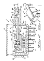
- Figures 1 through 3 illustrate an optoelectronics package 1 having an outer enclosure 2 comprising a box 3 with an open top 4 and a cover 5.
- Conductive electrical pins 6 are spaced apart in two rows and are encircled by insulative ceramic sleeves 7 mounted in a bottom wall 8 of the enclosure 2.
- a metal heat sink 9 is shown in Figure 4 having an L shape, and is secured on the bottom wall 8 between the rows of contacts 6 and against an end wall 10.
- a thermoelectric cooler 11 having end plates interconnected by coolant tubes is conductively soldered to the heat sink between the rows of contacts.
- thermoelectric cooler 11 is a known device which has a heat transfer rate that can be controlled by the application of an electrical current to a thermoelectric control circuit, not shown.
- a thermistor not shown, monitors the temperature of the cooler 11 and provides an output voltage in proportion to the temperature. The output voltage is sampled and used by the control circuit to control a current applied to the cooler.
- Figure 4 shows the heat sink 9 and cooler 11, which when soldered in the enclosure 2 are ready to receive a platform in the form of an optical bench 12.
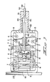
- Figures 2 and 5 illustrate the optical bench 12 in the form of an elongated platform 13 fabricated in one piece from heat conductive material.
- a planar surface 14 of the optical bench extends between a pair of laterally spaced apart pillars 15, 15 and perpendicular to an external datum surface 16 ⁇ on an end wall 16 having an opening 17 with an axis that is elevated and parallel with respect to the planar surface 14.
- a groove 18 is recessed angularly in the planar surface 14 near an end 19 opposite the end wall 16.
- a base 20 carries a semiconductor laser 21, shown schematically.
- the base 20 is fabricated from a plate of electrically insulative ceramic that has a metal film surface that is bonded to the surface 14 of the optical bench 12.
- a second base 22 of ceramic is mounted in the recess 18 and projects from the recess 18 at an angle with the planar surface 14.
- the second base 22 carries a PIN diode 23, shown schematically, in alignment with a rear facet of optical emission of the semiconductor laser 21.
- the laser 21 produces optical emission from two edges or facets.
- the PIN diode 23 monitors optical emission from a rear facet and produces an output voltage that is a measure of the emission being monitored.
- the diode 23 is angular with the axis of emission and is set back sufficiently to avoid reflection of emission reversely along the axis.
- the output voltage is sampled and used to control a voltage supply circuit, not shown, that supplies current to the laser 21, activating the laser 21 to produce optical emission.
- the optical bench 12 has a particular advantage in thermally coupling the laser 21, thereby eliminating the need for heat sink architecture within the semiconductor laser 21 itself.
- the pillars 15, 15 and the bottom of the optical bench 12 surround the laser 21 to provide a temperature modulator and a heat sink.
- the optical bench 12 is sufficiently thick to avoid warped distortion by thermal expansion or contraction with fluctuation in the operating temperature of the laser 21.
- the optical bench 12 is mounted by being soldered by its bottom surface 12 ⁇ to a top plate 24 of the thermoelectric cooler 11.
- the rate of heat conduction of the cooler 11 is electrically controlled according to known principles of operation. Heat is conducted away from the laser 21, to the optical bench 12, to the thermoelectric cooler 11, to the heat sink 9 and to the wall 10 of the package 1.
- a conductive mounting flange 25 in contact with the package 1 provides a means through which heat is dissipated or conducted away from the package 1.
- a lens assembly 26 comprises a hemispherical lens 27 having a diameter of about 2 millimeters and fabricated from optical quality silicon and coated with known antireflective optical coating.
- the lens 27 is assembled with a positioning means 28 including an optical diaphragm 29, a pedestal 30 against the lens 27 and the diaphragm 29 and a holder 31 constructed for attached mounting on the optical bench.
- the optical diaphragm 29 of metal has a diaphragm aperture 32 aligned with the spherical surface of the lens 27.
- the pedestal 30 is formed of thin metal with three legs 33, 33, 33 bent out of the plane of the thin metal and radially spaced about a central opening 34 in alignment with the diaphragm aperture 32.
- the legs 33, 33, 33 engage the spherical surface and hold the diaphragm 29 at a distance from the lens 27.
- the lens 27, pedestal 30 and diaphragm 29 are mounted in the lens holder 31 fabricated from copper and plated with nickel and then a layer of gold.
- the lens holder 31 has a wall 35 with a cylindrical opening 36 receiving the lens 27.
- the lens holder 31 has a plate 37 bonded externally to the wall 35.
- the plate 37 has an opening 38 less than the diameter of the opening 36 to provide a circular lip around the opening 37 against which the plano surface of the lens 27 engages.
- the diaphragm 29 is convex curved toward the lens 27. Trailing edges 39 of the curved diaphragm 29 seat against a bifurcated back wall 40 of the lens holder 35.
- the curved diaphragm 29 provides a leaf spring that urges the lens 27 to seat against the plate 37.
- the lens 27 is in fixed position on the lens assembly 26.
- the lens holder 31 has a planar bottom 41 and is adapted for precise mounting on the optical bench 12.
- the optical bench 12 is not yet mounted to the cooler 11.
- a vidicon 42 sights along an optical axis 43 along the optical bench 12 perpendicular to the datum surface 16 ⁇ and from the front facet of emission of the laser 21 and through the opening 17 of the optical bench.
- the laser 21 is temporarily activated to produce optical emission.
- the vidicon 42 focus is directed upon the front facet of optical emission and transmits an image of the emission to a CRT monitor 44.
- the vidicon 42 is of a type which can electronically generate a cross hair and overlay the cross hair at the focus. An image of the cross hair appears on the CRT 44.
- the lens assembly 26 is then placed on the optical bench 12 and is adjusted to a desired position on the optical bench 12 while maintaining the flat or plano surface of the hemispherical lens 27 parallel to the datum surface 16 ⁇ .
- the desired position is established when the lens 27 is focused upon the front facet of emission and the lens 27 transmits the emission precisely along the optical axis 43.
- the desired position becomes known by viewing the image of the emission on the CRT monitor 44, and watching the image of the emission shift as the lens assembly 26 is adjusted in position on the optical bench 12.
- the desired position of the lens assembly 26 is attained.
- the lens assembly 26 is clamped in place.
- the lens assembly 26 is aligned with zero tilt from direct alignment with the beam of laser emission.
- the tilt position may be adjusted before the lens assembly 26 is clamped in its final position.
- the clamped lens assembly 26 is secured by solder to the optical bench 12.
- the goal of the lens alignment is to align the axis of the focused beam to the axis of the fiber and yet avoid reflection from the fiber facet back into the laser. Maintaining reflection at the level of -50dB or less is critical to avoid spectral instability and deviations from linearity in the light versus current characteristic of the laser. This is best accomplished by beveling the fiber facet, also called the optical face, at an angle of 6_ or more. This angle is determined by the numerical aperture of the fiber. For a single mode fiber made of quartz, the resulting numerical aperture requires a bevel at an angle of 6_. This implies that the beam to be coupled must have a tilt angle equal to one-half the bevel angle of the fiber facet. The specific relationship is determined by the index of refraction of the fiber.
- a tilt angle must be added to the laser beam. This is done by aligning with zero tilt using the vidicon system and then displacing the lens by a predetermined amount to direct the beam to a tilted position from the zero tilt position. The resulting relationship between the tilt angle and the displacement is set by the magnification of the lens. In a typical system, magnification is 5 and a lens displacement of 7/10 of a mil will produce a tilt angle of 3_.
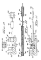
- Figures 9 and 10 show a length of optical fiber 45 having a relatively thick layer 46 of copper divided into segments 46, 46 adhered along the length of the fiber 45.
- the layer 46 is formed first by a minute thickness of copper that is applied by electroless deposition on the fiber 45 to provide a conductive surface.
- the conductive surface is then capable of receiving electrolytic deposition of additional copper to form the relatively thick layer 46.
- the segments 46, 46 are formed by selective deposition or by etching away the copper leaving only the segments 46, 46.
- a segment 46 is at one end 47 of the fiber 45 that is polished to provide an optical face 48.
- a fiber holder in the form of a first metal tube 49 concentrically encircles the end 47 of the fiber 45 and the segment 46, and is secured to the segment 46 with solder 50.
- the fiber 45 extends freely along the interior of the tube 49 and projects outwardly of an open end 51 of the tube 49.
- the other segment 46 is concentrically encircled by a fiber holder in the form of a second metal tube 52 spaced along the length of the fiber 45 from the tube 49.
- the second tube 52 is secured by solder 53 to the segment 46 forming an hermetic seal, and thereby to complete an optical fiber assembly 54.
- Figure 9 shows the optical fiber assembly 54 with the tube 49 surrounded concentrically by a sleeve bushing 55 having resilient fingers that radially grip the tube 49, and a radially outward projecting flange 47.
- the bushing 55 is placed against the wall 16 of the optical bench 12, with the tube 49 and the optical fiber 45 projecting through the opening 17 toward the lens 27 which was previously mounted on the optical bench 12.
- the optical face 48 of the fiber 45 is within the opening 17 and flush with the end of the interior 21 of the bushing 55.
- the bevel of the fiber facet is aligned with the bushing 55 and with the beam of laser emission.
- the laser 21 is temporarily activated to produce optical emission.
- the emission is transmitted by the lens 27 along the optical axis 43 and into the optical fiber 45 through its optical face 48 which faces toward the lens 27.
- the optical emission that emerges from the output end 58 of the optical fiber 45 is continuously measured for relative intensity. This measurement advantageously assists in locating the bushing 55 in a desired position.
- the desired position of the bushing 55 becomes known by viewing changes in the measured intensity as the position of the bushing 55 is adjusted. When the measure of intensity is at a relative maximum, the desired position of the bushing 55 is established.
- the bushing 55 is secured in desired position on the wall 16 by solder.
- the measurement of optical intensity is further advantageous in locating the optical face 48 of the optical fiber 45 in desired position along the optical axis 43.
- the position of the tube 49 is adjusted while the intensity of the optical emission is measured. More specifically, the tube 49 is moved with respect to the interior of the secured bushing 55, closer to or further from the lens 27, thereby causing a corresponding adjustment in position of the optical face 48 of the optical fiber 45 and a corresponding fluctuation of the measured intensity.
- the measure of intensity is at a relative maximum the desired position of the tube 49 and of the optical face 48 is established.
- the tube 49 in desired position is soldered to the interior of the bushing 55.
- the bushing 55, the tube 49, solder 50 and the corresponding segment of layer 46 provides positioning means for positioning the optical face 48 of the fiber 45 in desired position along the optical axis 43 and for mounting the fiber 45 to the optical bench 12.
- the optical bench 12 is shown in Figure 11 before mounting to the thermoelectric cooler 11.
- the optical bench 12 advantageously allows complete assembly of an optical coupling of the laser 21, lens 27 and optical fiber 45 before the optical bench 12 is inserted into the enclosure 2 and soldered to the plate 24 of the cooler 11.
- the bottom surface 12 ⁇ of the optical bench 12 can be soldered to a corresponding surface of the cooler 11 within the confines of the enclosure 2.
- the tubes 49, 52 and the optical fiber 45 project through an opening 59 through the wall 60 of the enclosure 2.
- a metal ferrule 61 has a radially projecting flange 62 for engaging against the wall 60, and an enlarged interior 63 for freely receiving the end of the tube 49 and the fiber 45.
- a reduced opening 64 through the end of the ferrule 65 encircles and frictionally grips the tube 52.
- the ferrule 61 is clamped in place by gripping the tube 52 and applies a column load on the fiber 45, which causes the fiber 45 to bend in relief of the applied column load, and of the internal stress of the fiber, into a continuous and smoothly curved configuration, with a large radius of curvature, substantially within the interior of the tube 52, and between the points of solder attachment 50, 53, and as shown by the dotted line 66 in Figures 2 and 10. Thereby a predetermined stress is applied to the attachment points.
- the ferrule 61 is secured by solder to the tube 52 and to the wall 60.
- the solder also forms hermetic seals between the ferrule 61 and the wall 60 and between the ferrule 61 and the tube 52.
- a solder shim not shown of precisely measured width is interposed between the flange 62 and the wall 60. The shim is melted, causing the shim to reduce in width and the flange 62 to move toward the wall 60 and become secured to the wall 60 upon solidification of the solder. Such movement of the flange 62 is accompanied by corresponding displacement of the tube 52, placing an axially or column load on the fiber 45.
- the fiber 45 is secured in desired position and is placed in a prestressed condition by means, including the ferrule 61 and bushing 55, and the tubes 49, 52 and the attachment points 50, 53, and, according to the following explanation.
- a strut assumed to be bent slightly from its axis, has a calculated strength to resist an increase in an axial directed compression load, or column load, despite an increase in bending of the strut.
- column load As the column load is increased and the strut is bent further, a point is reached whereby the strut can undergo a range of bent deflection without a corresponding increase in column load over the corresponding range of deflection.
- the optical bench 12 has the advantage of applying a column load upon the optical fiber 45 causing the fiber 43 to be bent slightly, and reaching the point whereby the fiber 45 can undergo a range of bent deflection without a corresponding increase in column load or a corresponding increase in stress applied to the attachment points.
- the tubes 49, 52 provide means for holding the fiber 45, and further means for applying a column load on the fiber 45.
- the contacts 16 provide electrical connections internally of the package 1 for the laser 21 and the PIN diode 23.
- small electrical wires are bonded or otherwise electrically joined, respectively, to the laser 21 and PIN diode 23 and to portions of selected contacts 16 that project into the package 1 through the bottom wall 8.
- Additional small electrical wires, not shown, are bonded or otherwise electrically joined, respectively, to the thermistor and the thermoelectric control of the cooler 11, and then to portions of selected contacts 16 that project into the package 1 through the bottom wall 8.
- the package 1 is immersed in a desired gaseous atmosphere.
- the cover 5 is then soldered to enclose the open top 4, thereby hermetically sealing the package 1.
- the package 1 is assembled in a series of soldering operations, as described. Each soldering operation uses a solder with slightly lower melting temperature than the melting temperature of solder used in a previous soldering operation.
- the package is assembled with different assemblies, which enables the number of soldering operations for the same assembly to be limited in number.
- solder alloy 80 parts Au, 20 parts Sn, has a melting temperature of 280_C, and is used in a first assembly to solder the heat sink 9 to the bottom wall 8 and to the cooler 11, and is used in another assembly as the solder 50 and 53 to solder the tubes 49 and 52 to the fiber 45, and is used in another assembly to solder the lens holder 35 to the optical bench 12.
- solder alloy 60 parts Pb, 40 parts In, has a melting temperature of 225_C and is used to solder the bushing 55 to the wall 16 and the tube 49.
- Solder alloy 52 parts In, 48 parts Sn has a melting temperature of 118_C, and is used to solder the cover 5 to the open top 4 of the package 1.
- the specific alloys are exemplary only, since other alloys also are useful in performing the soldering operations.
- the order of assembly of the parts comprising the package can be different than described, provided that the parts are assembled according to a procedure such that each soldering operation uses a solder with a melting temperature of at least 15_C lower than the melting temperature of solder used in a previous soldering operation.
Abstract
Description
- This invention relates to an optoelectronics package, and especially to a package with an hermetically sealed enclosure wherein a semiconductor laser is coupled optically with a lens, an optical fiber and a monitor of the optical emission of the laser.
- In the field of optoelectronics a semiconductor laser, also referred to as a laser diode, is a semiconductor device that emits coherent light from opposite edges or facets in response to an applied current. The light, or optical emission, from a front facet is useful as an optical carrier wave for communications signals. Construction of a semiconductor laser is known from various publications, some of which are identified in U.S. Patent 3,840,889. The patent also discloses an hermetically sealed enclosure for containing a semiconductor laser. Electrical terminals project from the interior of the enclosure to the exterior for connection to an electrical circuit that furnishes an applied current.
- U.S. Patent 4,003,074 discloses an optoelectronics package with an hermetically sealed enclosure containing a semiconductor laser and a monitor of optical emission from a rear facet of the semiconductor laser. A monitor, for example, a PIN diode, in response to the optical emission produces an output voltage for supply to an electrical circuit that controls the current applied to the semiconductor laser. The enclosure incorporates an optical lens for directing rays of optical emission in a narrow course externally of the enclosure.
- In many applications the emission from the laser must be coupled into an optical fiber. Coupling between an optical fiber and a semiconductor laser is subject to disadvantages and requires a high degree of care in fabrication. A direct attachment of an optical fiber to the laser can be disrupted, because the operating temperature of the laser will fluctuate and cause different dimensional changes respectively in the fiber and the laser. The dimensional changes in response to temperature fluctuation will cause the fiber to change position with respect to the laser or become separated from the laser.
- Direct coupling is generally inefficient because of a wide disparity in the dimensions of the guided modes in the laser and in the fiber. This can be overcome by the use of a lens for mode size matching.
- An optical coupling is subject to further disadvantages arising from use of a lens to focus optical emission from a laser on an optical fiber. It is difficult to achieve precision optical alignment of the lens and the laser. The fiber can become misaligned due to dimensional changes with temperature fluctuations.
- According to an aspect of the invention, an optoelectronics package with an hermetically sealed enclosure contains a semiconductor laser coupled optically with a lens and with an optical fiber that transmits optical emission of the laser externally of the enclosure.
- According to another aspect of the invention, the package includes an alignment fixture in the form of an optical bench that defines an optical axis with an origin at the front facet of the laser.
- According to another aspect of the invention, the lens is aligned with substantial precision along the optical axis and is focused upon the front facet. The lens transmits optical emission of the front facet into an end of the optical fiber aligned along the optical axis.
- According to another aspect of the invention, the lens is assembled with a positioning means including an optical diaphragm, a pedestal against the lens supporting the diaphragm and a holder constructed for attached mounting on the optical bench.
- According to another aspect of the invention, a portion of the optical fiber is anchored to the optical bench and another portion of the fiber is held by a ferrule that hermetically seals an opening of the enclosure through which the fiber projects and that applies a column load on the fiber such that the fiber ends are under a predetermined stress and stabilized against movement from or breakage from its anchored points over a range of operating temperatures of the laser.
- According to another aspect of the invention, the optical axis along the optical bench is established by a line of sight of a television camera focused upon a front facet of optical emission of the laser, and the lens with the positioning means on the optical bench is aligned with considerable accuracy using the line of sight and using the optical emission as the focus of the lens.
- According to an aspect of the invention, an alignment fixture in the form of an optical bench optically couples a semiconductor laser with a lens and with an optical fiber. The laser, lens and optical fiber are mounted on the optical bench before the optical bench is placed within the confines of an enclosure. The absence of the enclosure enables unobstructed manipulation of the parts into alignment on the optical bench.
- According to another aspect of the invention, the optical bench defines an optical axis with an origin at the front facet of the laser.
- According to another aspect of the invention, the lens is aligned with substantial precision along the optical axis and is focused upon the front facet. The lens transmits optical emission of the front facet into an end of the optical fiber aligned along the optical axis.
- According to another aspect of the invention, the lens is assembled with a positioning means including an optical diaphragm, a pedestal against the lens supporting the diaphragm and a holder constructed for attached mounting on the optical bench.
- According to another aspect of the invention, a portion of the optical fiber is anchored to the optical bench and another portion of the fiber is held by a tube that hermetically seals the fiber and that is useful for applying a column load on the fiber such that the fiber ends are under a predetermined stress and stabilized against movement from or breakage from its anchored points over a range of operating temperatures of the laser.
- According to another aspect of the invention, the optical axis along the optical bench is established by a line of sight of a television camera focused upon a front facet of optical emission of the laser, and the lens with the positioning means on the optical bench is aligned with considerable accuracy using the line of sight and using the optical emission as the focus of the lens.
- According to an aspect of the invention, a semiconductor laser, a lens and an optical fiber are optically coupled and are mounted on a optical bench that defines an optical axis with an origin at the front face of optical emission of the laser. A portion of the optical fiber is attached to a tube that facilitates anchoring of the optical fiber to the optical bench. Another portion of the fiber is held by a tube that is fastened to the fiber by an attachment technique that forms an hermetic seal with the periphery of the fiber.
- According to another aspect of the invention, the tubes are useful for mounting the fiber, for example, in an optoelectronics package, and for applying a column load on the fiber such that the fiber points of attachment are under a predetermined stress and stabilized against movement from or breakage from its attachment points over a range of dimensional changes in the fiber due to fluctuations in temperature.
- According to another aspect of the invention, the fiber length between its attachment points is free to bend to a smoothly curved configuration in relief of the applied stress. The curved configuration is contained substantially within the confines of a corresponding tube.
- According to another aspect of the invention, the corresponding attachments of the fiber with the tube are fabricated by spaced segments of conductive material adhered to the fiber, followed by relatively thick layer of conductive material that are joined by solder to the corresponding tubes.
- Other advantages of the invention will be apparent by way of example from a detailed description that follows and from accompanying drawings, which together disclose, by way of example, embodiments of the invention.
- In the drawings,
- FIGURE 1 is a perspective view of an optoelectronics package for a semiconductor laser.
- FIGURE 2 is an enlarged elevation view in section of the package shown in Figure 1 with a cover shown exploded.
- FIGURE 3 is an enlarged top view of a longitudinal section of the package shown in Figure 1.
- FIGURE 4 is an enlarged perspective view with a part cut away and with parts exploded to illustrate an enclosure, a thermoelectric cooler and a heat sink of the package shown in Figure 1.
- FIGURE 5 is an enlarged perspective view with parts exploded to illustrate an optical bench, a semiconductor laser and a monitor of facet emission.
- FIGURE 6 is an enlarged top view of a lens assembly for the package shown in Figure 1.
- FIGURE 7 is an enlarged perspective view with parts exploded of the lens assembly shown in Figure 6.
- FIGURE 8 is a diagrammatic view illustrating a technique for alignment of the semiconductor laser and lens assembly along an optical axis of the optical bench.
- FIGURE 9 is an enlarged perspective view of an optical fiber assembly with parts exploded.
- FIGURE 10 is an enlarged longitudinal section view of a portion of the optical fiber assembly shown in Figure 8.
- FIGURE 11 is an enlarged elevation in section of the optical bench before mounting in the package.
- With reference to the drawings, Figures 1 through 3 illustrate an optoelectronics package 1 having an
outer enclosure 2 comprising abox 3 with anopen top 4 and acover 5. Conductiveelectrical pins 6 are spaced apart in two rows and are encircled by insulativeceramic sleeves 7 mounted in abottom wall 8 of theenclosure 2. Ametal heat sink 9 is shown in Figure 4 having an L shape, and is secured on thebottom wall 8 between the rows ofcontacts 6 and against anend wall 10. A thermoelectric cooler 11 having end plates interconnected by coolant tubes is conductively soldered to the heat sink between the rows of contacts. - A thermoelectric cooler 11 is a known device which has a heat transfer rate that can be controlled by the application of an electrical current to a thermoelectric control circuit, not shown. A thermistor, not shown, monitors the temperature of the cooler 11 and provides an output voltage in proportion to the temperature. The output voltage is sampled and used by the control circuit to control a current applied to the cooler. Figure 4 shows the
heat sink 9 and cooler 11, which when soldered in theenclosure 2 are ready to receive a platform in the form of anoptical bench 12. - Figures 2 and 5 illustrate the
optical bench 12 in the form of anelongated platform 13 fabricated in one piece from heat conductive material. Aplanar surface 14 of the optical bench extends between a pair of laterally spaced apartpillars end wall 16 having anopening 17 with an axis that is elevated and parallel with respect to theplanar surface 14. Agroove 18 is recessed angularly in theplanar surface 14 near anend 19 opposite theend wall 16. A base 20 carries asemiconductor laser 21, shown schematically. Thebase 20 is fabricated from a plate of electrically insulative ceramic that has a metal film surface that is bonded to thesurface 14 of theoptical bench 12. Asecond base 22 of ceramic is mounted in therecess 18 and projects from therecess 18 at an angle with theplanar surface 14. Thesecond base 22 carries aPIN diode 23, shown schematically, in alignment with a rear facet of optical emission of thesemiconductor laser 21. - According to known principles of operation, the
laser 21 produces optical emission from two edges or facets. ThePIN diode 23 monitors optical emission from a rear facet and produces an output voltage that is a measure of the emission being monitored. Thediode 23 is angular with the axis of emission and is set back sufficiently to avoid reflection of emission reversely along the axis. The output voltage is sampled and used to control a voltage supply circuit, not shown, that supplies current to thelaser 21, activating thelaser 21 to produce optical emission. - The
optical bench 12 has a particular advantage in thermally coupling thelaser 21, thereby eliminating the need for heat sink architecture within thesemiconductor laser 21 itself. Thepillars optical bench 12 surround thelaser 21 to provide a temperature modulator and a heat sink. Theoptical bench 12 is sufficiently thick to avoid warped distortion by thermal expansion or contraction with fluctuation in the operating temperature of thelaser 21. Theoptical bench 12 is mounted by being soldered by its bottom surface 12ʹ to atop plate 24 of the thermoelectric cooler 11. The rate of heat conduction of the cooler 11 is electrically controlled according to known principles of operation. Heat is conducted away from thelaser 21, to theoptical bench 12, to the thermoelectric cooler 11, to theheat sink 9 and to thewall 10 of the package 1. A conductive mountingflange 25 in contact with the package 1 provides a means through which heat is dissipated or conducted away from the package 1. - The
optical bench 12 advantageously provides a means for optically coupling thelaser 21. With reference to Figures 6 and 7, alens assembly 26 comprises ahemispherical lens 27 having a diameter of about 2 millimeters and fabricated from optical quality silicon and coated with known antireflective optical coating. Thelens 27 is assembled with a positioning means 28 including anoptical diaphragm 29, apedestal 30 against thelens 27 and thediaphragm 29 and aholder 31 constructed for attached mounting on the optical bench. Theoptical diaphragm 29 of metal has adiaphragm aperture 32 aligned with the spherical surface of thelens 27. Thepedestal 30 is formed of thin metal with threelegs central opening 34 in alignment with thediaphragm aperture 32. Thelegs diaphragm 29 at a distance from thelens 27. - The
lens 27,pedestal 30 anddiaphragm 29 are mounted in thelens holder 31 fabricated from copper and plated with nickel and then a layer of gold. Thelens holder 31 has awall 35 with acylindrical opening 36 receiving thelens 27. Thelens holder 31 has aplate 37 bonded externally to thewall 35. Theplate 37 has anopening 38 less than the diameter of theopening 36 to provide a circular lip around theopening 37 against which the plano surface of thelens 27 engages. Thediaphragm 29 is convex curved toward thelens 27. Trailingedges 39 of thecurved diaphragm 29 seat against abifurcated back wall 40 of thelens holder 35. Thecurved diaphragm 29 provides a leaf spring that urges thelens 27 to seat against theplate 37. Thelens 27 is in fixed position on thelens assembly 26. Thelens holder 31 has a planar bottom 41 and is adapted for precise mounting on theoptical bench 12. - As shown in Figure 8, the
optical bench 12 is not yet mounted to the cooler 11. Avidicon 42 sights along anoptical axis 43 along theoptical bench 12 perpendicular to the datum surface 16ʹ and from the front facet of emission of thelaser 21 and through theopening 17 of the optical bench. Thelaser 21 is temporarily activated to produce optical emission. Thevidicon 42 focus is directed upon the front facet of optical emission and transmits an image of the emission to aCRT monitor 44. Thevidicon 42 is of a type which can electronically generate a cross hair and overlay the cross hair at the focus. An image of the cross hair appears on theCRT 44. Thelens assembly 26 is then placed on theoptical bench 12 and is adjusted to a desired position on theoptical bench 12 while maintaining the flat or plano surface of thehemispherical lens 27 parallel to the datum surface 16ʹ. The desired position is established when thelens 27 is focused upon the front facet of emission and thelens 27 transmits the emission precisely along theoptical axis 43. The desired position becomes known by viewing the image of the emission on theCRT monitor 44, and watching the image of the emission shift as thelens assembly 26 is adjusted in position on theoptical bench 12. When the image of the emission on the CRT monitor 44 coincides with the cross hair image of theCRT monitor 44, the desired position of thelens assembly 26 is attained. Thelens assembly 26 is clamped in place. Thelens assembly 26 is aligned with zero tilt from direct alignment with the beam of laser emission. The tilt position may be adjusted before thelens assembly 26 is clamped in its final position. The clampedlens assembly 26 is secured by solder to theoptical bench 12. - The goal of the lens alignment is to align the axis of the focused beam to the axis of the fiber and yet avoid reflection from the fiber facet back into the laser. Maintaining reflection at the level of -50dB or less is critical to avoid spectral instability and deviations from linearity in the light versus current characteristic of the laser. This is best accomplished by beveling the fiber facet, also called the optical face, at an angle of 6_ or more. This angle is determined by the numerical aperture of the fiber. For a single mode fiber made of quartz, the resulting numerical aperture requires a bevel at an angle of 6_. This implies that the beam to be coupled must have a tilt angle equal to one-half the bevel angle of the fiber facet. The specific relationship is determined by the index of refraction of the fiber. Thus, a tilt angle must be added to the laser beam. This is done by aligning with zero tilt using the vidicon system and then displacing the lens by a predetermined amount to direct the beam to a tilted position from the zero tilt position. The resulting relationship between the tilt angle and the displacement is set by the magnification of the lens. In a typical system, magnification is 5 and a lens displacement of 7/10 of a mil will produce a tilt angle of 3_.
- Figures 9 and 10 show a length of
optical fiber 45 having a relativelythick layer 46 of copper divided intosegments fiber 45. Thelayer 46 is formed first by a minute thickness of copper that is applied by electroless deposition on thefiber 45 to provide a conductive surface. The conductive surface is then capable of receiving electrolytic deposition of additional copper to form the relativelythick layer 46. Thesegments segments segment 46 is at one end 47 of thefiber 45 that is polished to provide anoptical face 48. A fiber holder in the form of afirst metal tube 49 concentrically encircles the end 47 of thefiber 45 and thesegment 46, and is secured to thesegment 46 with solder 50. Thereby, a limited length of thefiber 45 adjacent to itsoptical face 48 is secured to the interior of thetube 49. Thefiber 45 extends freely along the interior of thetube 49 and projects outwardly of anopen end 51 of thetube 49. Theother segment 46 is concentrically encircled by a fiber holder in the form of asecond metal tube 52 spaced along the length of thefiber 45 from thetube 49. Thesecond tube 52 is secured bysolder 53 to thesegment 46 forming an hermetic seal, and thereby to complete anoptical fiber assembly 54. - Figure 9 shows the
optical fiber assembly 54 with thetube 49 surrounded concentrically by asleeve bushing 55 having resilient fingers that radially grip thetube 49, and a radially outward projecting flange 47. As shown in Figures 5 and 11, thebushing 55 is placed against thewall 16 of theoptical bench 12, with thetube 49 and theoptical fiber 45 projecting through theopening 17 toward thelens 27 which was previously mounted on theoptical bench 12. Initially theoptical face 48 of thefiber 45 is within theopening 17 and flush with the end of the interior 21 of thebushing 55. The bevel of the fiber facet is aligned with thebushing 55 and with the beam of laser emission. - The
laser 21 is temporarily activated to produce optical emission. The emission is transmitted by thelens 27 along theoptical axis 43 and into theoptical fiber 45 through itsoptical face 48 which faces toward thelens 27. According to known techniques the optical emission that emerges from theoutput end 58 of theoptical fiber 45 is continuously measured for relative intensity. This measurement advantageously assists in locating thebushing 55 in a desired position. The desired position of thebushing 55 becomes known by viewing changes in the measured intensity as the position of thebushing 55 is adjusted. When the measure of intensity is at a relative maximum, the desired position of thebushing 55 is established. Thebushing 55 is secured in desired position on thewall 16 by solder. - The measurement of optical intensity is further advantageous in locating the
optical face 48 of theoptical fiber 45 in desired position along theoptical axis 43. With thebushing 55 secured in place, the position of thetube 49 is adjusted while the intensity of the optical emission is measured. More specifically, thetube 49 is moved with respect to the interior of thesecured bushing 55, closer to or further from thelens 27, thereby causing a corresponding adjustment in position of theoptical face 48 of theoptical fiber 45 and a corresponding fluctuation of the measured intensity. When the measure of intensity is at a relative maximum the desired position of thetube 49 and of theoptical face 48 is established. Thetube 49 in desired position is soldered to the interior of thebushing 55. Thebushing 55, thetube 49, solder 50 and the corresponding segment oflayer 46 provides positioning means for positioning theoptical face 48 of thefiber 45 in desired position along theoptical axis 43 and for mounting thefiber 45 to theoptical bench 12. - The
optical bench 12 is shown in Figure 11 before mounting to the thermoelectric cooler 11. Theoptical bench 12 advantageously allows complete assembly of an optical coupling of thelaser 21,lens 27 andoptical fiber 45 before theoptical bench 12 is inserted into theenclosure 2 and soldered to theplate 24 of the cooler 11. The bottom surface 12ʹ of theoptical bench 12 can be soldered to a corresponding surface of the cooler 11 within the confines of theenclosure 2. As shown in Figure 2, thetubes optical fiber 45 project through anopening 59 through thewall 60 of theenclosure 2. Ametal ferrule 61 has aradially projecting flange 62 for engaging against thewall 60, and anenlarged interior 63 for freely receiving the end of thetube 49 and thefiber 45. A reducedopening 64 through the end of theferrule 65 encircles and frictionally grips thetube 52. Theferrule 61 is clamped in place by gripping thetube 52 and applies a column load on thefiber 45, which causes thefiber 45 to bend in relief of the applied column load, and of the internal stress of the fiber, into a continuous and smoothly curved configuration, with a large radius of curvature, substantially within the interior of thetube 52, and between the points ofsolder attachment 50, 53, and as shown by the dottedline 66 in Figures 2 and 10. Thereby a predetermined stress is applied to the attachment points. Theferrule 61 is secured by solder to thetube 52 and to thewall 60. The solder also forms hermetic seals between theferrule 61 and thewall 60 and between theferrule 61 and thetube 52. A solder shim not shown of precisely measured width is interposed between theflange 62 and thewall 60. The shim is melted, causing the shim to reduce in width and theflange 62 to move toward thewall 60 and become secured to thewall 60 upon solidification of the solder. Such movement of theflange 62 is accompanied by corresponding displacement of thetube 52, placing an axially or column load on thefiber 45. - The
fiber 45 is secured in desired position and is placed in a prestressed condition by means, including theferrule 61 andbushing 55, and thetubes optical bench 12 has the advantage of applying a column load upon theoptical fiber 45 causing thefiber 43 to be bent slightly, and reaching the point whereby thefiber 45 can undergo a range of bent deflection without a corresponding increase in column load or a corresponding increase in stress applied to the attachment points. Thereafter, fluctuation of the operating temperature of thelaser 21, that causes corresponding thermal expansion or contraction of thefiber 45, will cause corresponding fluctuation in bending deflection of thefiber 45 within the range of bent deflection without an increase in column load, which column load would be transmitted to the attachment points 50, 53 of thefiber 45 and would subject the anchoring points, or attachment points 50, 53, to undue strain or breakage, or cause theoptical face 48 of thefiber 45 to shift away from its desired position where the relative maximum amount of optical emission is transmitted from thelens 27 to theoptical face 48. Thetubes fiber 45, and further means for applying a column load on thefiber 45. - The
contacts 16 provide electrical connections internally of the package 1 for thelaser 21 and thePIN diode 23. For example, according to known techniques, small electrical wires, not shown, are bonded or otherwise electrically joined, respectively, to thelaser 21 andPIN diode 23 and to portions of selectedcontacts 16 that project into the package 1 through thebottom wall 8. Additional small electrical wires, not shown, are bonded or otherwise electrically joined, respectively, to the thermistor and the thermoelectric control of the cooler 11, and then to portions of selectedcontacts 16 that project into the package 1 through thebottom wall 8. The package 1 is immersed in a desired gaseous atmosphere. Thecover 5 is then soldered to enclose the open top 4, thereby hermetically sealing the package 1. - The package 1 is assembled in a series of soldering operations, as described. Each soldering operation uses a solder with slightly lower melting temperature than the melting temperature of solder used in a previous soldering operation. The package is assembled with different assemblies, which enables the number of soldering operations for the same assembly to be limited in number. For example, solder alloy, 80 parts Au, 20 parts Sn, has a melting temperature of 280_C, and is used in a first assembly to solder the
heat sink 9 to thebottom wall 8 and to the cooler 11, and is used in another assembly as thesolder 50 and 53 to solder thetubes fiber 45, and is used in another assembly to solder thelens holder 35 to theoptical bench 12. Thelaser 21,base 20,diode 23 andbase 22 have been secured on the optical bench according to known techniques for high temperature, ceramic to metal bonding that is not disturbed by temperatures related to soldering operations. Solder alloy, 60 parts Pb, 40 parts In, has a melting temperature of 225_C and is used to solder thebushing 55 to thewall 16 and thetube 49. Solder alloy 70 parts In, 30 parts Pb, has a melting temperature of 174_C and is used to solder theoptical bench 12 to theplate 25 of the cooler 11. Solder alloy 97 parts In, 3 parts Ag, has a melting temperature of 143_C, and is used to solder theferrule 61 to thewall 60 and thetube 52.Solder alloy 52 parts In, 48 parts Sn, has a melting temperature of 118_C, and is used to solder thecover 5 to theopen top 4 of the package 1. The specific alloys are exemplary only, since other alloys also are useful in performing the soldering operations. The order of assembly of the parts comprising the package can be different than described, provided that the parts are assembled according to a procedure such that each soldering operation uses a solder with a melting temperature of at least 15_C lower than the melting temperature of solder used in a previous soldering operation. - The invention has been disclosed by way of example with reference to the description and drawings. Other examples of the invention are intended to be covered by the spirit and scope of the claims.
Claims (10)
an optical bench (12) is in the enclosure (2) and along which is defined an optical axis (43),
the semiconductor laser (21) is mounted on the optical bench (12) with the front facet along the optical axis (43),
the monitor (23) is mounted on the optical bench for receiving optical emission from the rear facet,
a lens (27) is focused on the front facet for transmitting optical emission from the front facet along the optical axis (43),
the lens (27) is positioned at a desired location on the optical bench (12), and
the optical fiber (45) has a first optical face (48) aligned by a positioning means (49,50,55) with the optical axis (43)and a second optical face projecting to an exterior of the enclosure (2).
the positioning means (49,50,55)is secured to the optical fiber (45) for applying a column load on the fiber (45), and a length of the fiber is smoothly curved in relief of the applied column load.
an optical diaphragm (29) is mounted on the optical bench (12) between the lens (27) and the first optical face (48), a diaphragm aperture (32) of the optical diaphragm (29) is aligned with the optical axis (43), a pedestal (30) is against said lens (27) supporting said optical diaphragm (29), and a holder (31) on the optical bench (12), the holder (31) retaining the lens (27), the optical diaphragm (29) and the pedestal (30).
a length of the fiber (45) is smoothly curved in relief of the applied column load.
a semiconductor laser (4) with a front facet of optical emission along an optical axis (43),
a monitor (23) of optical emission for receiving optical emission from a rear facet of optical emission,
a lens (27) focused on the front facet for transmitting optical emission from the front facet along the optical axis (43),
an optical fiber (45) with an optical face (48) aligned with the optical axis (43), characterized in that;
the laser (21), the monitor (23), the lens (27) and the fiber (45) are on an optical bench (12) along which is defined an optical axis (43),
a datum surface (16ʹ) is on the bench for aligning the lens (27) and for aligning the optical axis (43).
the datum surface (16ʹ) is on an end wall (16) of the optical bench (12), and an aperture (17) through the end wall (16) is aligned with the optical axis (43).
a tube (49) surrounds the fiber (45), and a bushing (55) surrounds the tube (49) and is joined to the optical bench (12).
a length of optical fiber (45) having an optical face (48),
a tube (49) joined to the fiber (45), characterized in that;
means (61,52,53) are connected to the fiber (45) for applying a column load on the fiber (45) and for causing the fiber (45) to bend in a smoothly curved configuration within the interior of the tube (49).
the means (61,52,53,46) includes a second segment of conductive material (46) on the surface of the fiber (45), a conductive second tube (52) and material (53) joining the second tube (52) and second segment of conductive material (46) and forming an hermetic seal.
Applications Claiming Priority (6)
| Application Number | Priority Date | Filing Date | Title |
|---|---|---|---|
| US06/902,374 US4762386A (en) | 1986-09-02 | 1986-09-02 | Optical fiber assembly including means utilizing a column load to compensate for thermal effects |
| US902998 | 1986-09-02 | ||
| US06/902,998 US4818053A (en) | 1986-09-02 | 1986-09-02 | Optical bench for a semiconductor laser and method |
| US902374 | 1986-09-02 | ||
| US06/902,997 US4752109A (en) | 1986-09-02 | 1986-09-02 | Optoelectronics package for a semiconductor laser |
| US902997 | 1992-06-23 |
Publications (2)
| Publication Number | Publication Date |
|---|---|
| EP0259018A1 true EP0259018A1 (en) | 1988-03-09 |
| EP0259018B1 EP0259018B1 (en) | 1991-10-16 |
Family
ID=27420594
Family Applications (1)
| Application Number | Title | Priority Date | Filing Date |
|---|---|---|---|
| EP87306979A Expired - Lifetime EP0259018B1 (en) | 1986-09-02 | 1987-08-06 | Optoelectronics package for a semiconductor laser |
Country Status (4)
| Country | Link |
|---|---|
| EP (1) | EP0259018B1 (en) |
| JP (1) | JP2627900B2 (en) |
| KR (1) | KR880004611A (en) |
| DE (1) | DE3773810D1 (en) |
Cited By (17)
| Publication number | Priority date | Publication date | Assignee | Title |
|---|---|---|---|---|
| EP0364672A2 (en) * | 1988-10-20 | 1990-04-25 | Deutsche Aerospace AG | Laser diode configuration with an integrated drive circuit |
| GB2229856A (en) * | 1989-03-31 | 1990-10-03 | Stc Plc | Electro-optic transducer and sheet-metal microlens holder |
| EP0392719A2 (en) * | 1989-04-08 | 1990-10-17 | Gec-Marconi Limited | Optical coupling arrangements |
| GB2234088A (en) * | 1989-07-05 | 1991-01-23 | Mitsubishi Electric Corp | Optical semiconductor module |
| EP0412184A1 (en) * | 1989-08-09 | 1991-02-13 | Siemens Aktiengesellschaft | Optoelectronic converter with lens-coupling optics |
| EP0444610A2 (en) * | 1990-03-02 | 1991-09-04 | Gte Laboratories Incorporated | Uptapered single-mode optical fiber package for optoelectronic components |
| EP0484167A1 (en) * | 1990-10-31 | 1992-05-06 | Nec Corporation | Laser diode module with pigtail fiber |
| EP0511931A2 (en) * | 1991-04-29 | 1992-11-04 | International Business Machines Corporation | An apparatus and a method for an optical fiber interface |
| US5241614A (en) * | 1991-04-29 | 1993-08-31 | International Business Machines Corporation | Apparatus and a method for an optical fiber interface |
| EP0763760A1 (en) * | 1995-07-07 | 1997-03-19 | Nec Corporation | Semiconductor laser module |
| GB2312526A (en) * | 1996-04-23 | 1997-10-29 | Baillie Hamilton William John | Light emitting device housed in a containment |
| EP0860914A2 (en) * | 1997-02-13 | 1998-08-26 | Nec Corporation | Semiconductor laser module |
| EP0948104A2 (en) * | 1998-03-30 | 1999-10-06 | Sumitomo Electric Industries, Ltd. | Semiconductor laser module and method of manufacturing the same |
| WO2002082147A2 (en) * | 2001-04-05 | 2002-10-17 | Unique-M.O.D.E. Ag | Optical or optoelectronic array |
| GB2390911A (en) * | 2002-06-14 | 2004-01-21 | Furukawa Electric Co Ltd | Optic fibre semiconductor module package |
| EP1492208A3 (en) * | 2003-06-27 | 2005-01-26 | NEC Corporation | Semiconductor laser module and method of assembling the same |
| CN113131330A (en) * | 2021-03-31 | 2021-07-16 | 杭州耀芯科技有限公司 | Laser luminous power monitoring system, monitoring method and collimating lens thereof |
Families Citing this family (4)
| Publication number | Priority date | Publication date | Assignee | Title |
|---|---|---|---|---|
| JP2681032B2 (en) * | 1994-07-26 | 1997-11-19 | 山形大学長 | Ferroelectric polymer single crystal, manufacturing method thereof, and piezoelectric element, pyroelectric element and nonlinear optical element using the same |
| CN103944062A (en) * | 2014-04-29 | 2014-07-23 | 鞍山创鑫激光技术有限公司 | Semiconductor laser unit of single chip optical fiber coupling output |
| DE102016102327B4 (en) * | 2016-02-10 | 2018-02-08 | Schott Ag | Housing for an electronic component and laser module |
| CN108092130B (en) * | 2017-12-25 | 2019-10-01 | 北京凯普林光电科技股份有限公司 | A kind of capsulation structure for semiconductor laser |
Citations (1)
| Publication number | Priority date | Publication date | Assignee | Title |
|---|---|---|---|---|
| EP0152932A2 (en) * | 1984-02-17 | 1985-08-28 | Siemens Aktiengesellschaft | Protection tube for glass fibre |
Family Cites Families (2)
| Publication number | Priority date | Publication date | Assignee | Title |
|---|---|---|---|---|
| JPS58106513A (en) * | 1981-12-19 | 1983-06-24 | Sumitomo Electric Ind Ltd | Optical connector |
| JPS5947789A (en) * | 1982-09-10 | 1984-03-17 | Nec Corp | Photo semiconductor module equipped with optical fiber |
-
1987
- 1987-08-06 EP EP87306979A patent/EP0259018B1/en not_active Expired - Lifetime
- 1987-08-06 DE DE8787306979T patent/DE3773810D1/en not_active Expired - Fee Related
- 1987-09-01 KR KR870009639A patent/KR880004611A/en not_active Application Discontinuation
- 1987-09-02 JP JP62220092A patent/JP2627900B2/en not_active Expired - Lifetime
Patent Citations (1)
| Publication number | Priority date | Publication date | Assignee | Title |
|---|---|---|---|---|
| EP0152932A2 (en) * | 1984-02-17 | 1985-08-28 | Siemens Aktiengesellschaft | Protection tube for glass fibre |
Non-Patent Citations (3)
| Title |
|---|
| NACHRICHTENTECHNISCHE ZEITSCHRIFT N.T.Z., vol. 39, no. 5, May 1986, pages 318-320,322,323, Berlin, DE; A. KUKE et al.: "Verfahren zur automatischen Montage und Justierung optischer Bausteine" * |
| PATENT ABSTRACTS OF JAPAN, vol. 9, no. 126 (E-318)[1849], 31st May 1985; & JP-A-60 12 786 (HITACHI SEISAKUSHO K.K.) 23-01-1985 * |
| PATENT ABSTRACTS OF JAPAN, vol. 9, no. 20 (P-330)[1743], 26th January 1985; & JP-A-59 166 906 (NIPPON DENSHIN DENWA KOSHA) 20-09-1984 * |
Cited By (34)
| Publication number | Priority date | Publication date | Assignee | Title |
|---|---|---|---|---|
| EP0364672A2 (en) * | 1988-10-20 | 1990-04-25 | Deutsche Aerospace AG | Laser diode configuration with an integrated drive circuit |
| EP0364672A3 (en) * | 1988-10-20 | 1991-03-20 | Deutsche Aerospace AG | Laser diode configuration with an integrated drive circuit |
| GB2229856B (en) * | 1989-03-31 | 1993-04-21 | Stc Plc | Electro-optic transducer assembly |
| GB2229856A (en) * | 1989-03-31 | 1990-10-03 | Stc Plc | Electro-optic transducer and sheet-metal microlens holder |
| EP0392719A2 (en) * | 1989-04-08 | 1990-10-17 | Gec-Marconi Limited | Optical coupling arrangements |
| EP0392719A3 (en) * | 1989-04-08 | 1991-11-06 | Gec-Marconi Limited | Optical coupling arrangements |
| GB2234088A (en) * | 1989-07-05 | 1991-01-23 | Mitsubishi Electric Corp | Optical semiconductor module |
| GB2234088B (en) * | 1989-07-05 | 1993-07-14 | Mitsubishi Electric Corp | Optical semiconductor module |
| EP0412184A1 (en) * | 1989-08-09 | 1991-02-13 | Siemens Aktiengesellschaft | Optoelectronic converter with lens-coupling optics |
| EP0444610A3 (en) * | 1990-03-02 | 1992-08-12 | Gte Laboratories Incorporated | Uptapered single-mode optical fiber package for optoelectronic components |
| EP0444610A2 (en) * | 1990-03-02 | 1991-09-04 | Gte Laboratories Incorporated | Uptapered single-mode optical fiber package for optoelectronic components |
| EP0484167A1 (en) * | 1990-10-31 | 1992-05-06 | Nec Corporation | Laser diode module with pigtail fiber |
| US5247530A (en) * | 1990-10-31 | 1993-09-21 | Nec Corporation | Laser diode module |
| EP0511931A2 (en) * | 1991-04-29 | 1992-11-04 | International Business Machines Corporation | An apparatus and a method for an optical fiber interface |
| EP0511931A3 (en) * | 1991-04-29 | 1993-03-31 | International Business Machines Corporation | An apparatus and a method for an optical fiber interface |
| US5241614A (en) * | 1991-04-29 | 1993-08-31 | International Business Machines Corporation | Apparatus and a method for an optical fiber interface |
| EP0763760A1 (en) * | 1995-07-07 | 1997-03-19 | Nec Corporation | Semiconductor laser module |
| US5673349A (en) * | 1995-07-07 | 1997-09-30 | Nec Corporation | Semiconductor laser module |
| GB2312526A (en) * | 1996-04-23 | 1997-10-29 | Baillie Hamilton William John | Light emitting device housed in a containment |
| EP0860914A2 (en) * | 1997-02-13 | 1998-08-26 | Nec Corporation | Semiconductor laser module |
| EP0860914A3 (en) * | 1997-02-13 | 1998-09-16 | Nec Corporation | Semiconductor laser module |
| US5963697A (en) * | 1997-02-13 | 1999-10-05 | Nec Corporation | Semiconductor laser module |
| EP0948104A2 (en) * | 1998-03-30 | 1999-10-06 | Sumitomo Electric Industries, Ltd. | Semiconductor laser module and method of manufacturing the same |
| EP0948104A3 (en) * | 1998-03-30 | 1999-10-27 | Sumitomo Electric Industries, Ltd. | Semiconductor laser module and method of manufacturing the same |
| US6244754B1 (en) | 1998-03-30 | 2001-06-12 | Sumitomo Electric Industries, Ltd. | Semiconductor laser module and method of manufacturing the same |
| WO2002082147A2 (en) * | 2001-04-05 | 2002-10-17 | Unique-M.O.D.E. Ag | Optical or optoelectronic array |
| WO2002082147A3 (en) * | 2001-04-05 | 2004-01-08 | Unique M O D E Ag | Optical or optoelectronic array |
| GB2390911A (en) * | 2002-06-14 | 2004-01-21 | Furukawa Electric Co Ltd | Optic fibre semiconductor module package |
| US7477810B2 (en) | 2002-06-14 | 2009-01-13 | The Furukawa Electric Co., Ltd. | Optical semiconductor module |
| US7738747B2 (en) | 2002-06-14 | 2010-06-15 | The Furukawa Electric Co., Ltd. | Optical semiconductor module |
| US8000567B2 (en) | 2002-06-14 | 2011-08-16 | The Furukawa Electric Co., Ltd. | Optical semiconductor module |
| EP1492208A3 (en) * | 2003-06-27 | 2005-01-26 | NEC Corporation | Semiconductor laser module and method of assembling the same |
| US7308012B2 (en) | 2003-06-27 | 2007-12-11 | Nec Corporation | Semiconductor laser module and method of assembling the same |
| CN113131330A (en) * | 2021-03-31 | 2021-07-16 | 杭州耀芯科技有限公司 | Laser luminous power monitoring system, monitoring method and collimating lens thereof |
Also Published As
| Publication number | Publication date |
|---|---|
| KR880004611A (en) | 1988-06-07 |
| EP0259018B1 (en) | 1991-10-16 |
| JPS6364008A (en) | 1988-03-22 |
| DE3773810D1 (en) | 1991-11-21 |
| JP2627900B2 (en) | 1997-07-09 |
Similar Documents
| Publication | Publication Date | Title |
|---|---|---|
| US4752109A (en) | Optoelectronics package for a semiconductor laser | |
| EP0259018B1 (en) | Optoelectronics package for a semiconductor laser | |
| US4818053A (en) | Optical bench for a semiconductor laser and method | |
| US4548466A (en) | Optical fibre coupling assemblies | |
| US4615031A (en) | Injection laser packages | |
| US4762386A (en) | Optical fiber assembly including means utilizing a column load to compensate for thermal effects | |
| US4920262A (en) | Photoelectric device with leads | |
| US5068865A (en) | Semiconductor laser module | |
| GB2124402A (en) | Injection laser packages | |
| US4281891A (en) | Device for excellently coupling a laser beam to a transmission medium through a lens | |
| US5127072A (en) | Laser module with compliant optical fiber coupling | |
| KR0151717B1 (en) | Optoelectronic arrangement having a coupling between an optical transmission fibre and a semiconductor laser diode | |
| US5673350A (en) | Laser module with focusing lens and fixing method of the focusing lens | |
| US4144504A (en) | Planar laser mount | |
| JPH03102305A (en) | Multiple fiber alignment type package for inclined surface type optoelectronics part | |
| US6595701B2 (en) | Laser diode module | |
| US4762395A (en) | Lens assembly for optical coupling with a semiconductor laser | |
| US5247530A (en) | Laser diode module | |
| EP0620460A1 (en) | Semiconductor element module | |
| JPS62906A (en) | Electrooptic transducer | |
| AU6602690A (en) | Mounting optical components | |
| KR20000055460A (en) | Apparatus for aligning optical source with optical fiber and optical source module comprising it | |
| US4997279A (en) | Optical bench for a semiconductor laser and method | |
| US6178188B1 (en) | Laser assembly platform with silicon base | |
| US20050047731A1 (en) | Packaging assembly for optical subassembly |
Legal Events
| Date | Code | Title | Description |
|---|---|---|---|
| PUAI | Public reference made under article 153(3) epc to a published international application that has entered the european phase |
Free format text: ORIGINAL CODE: 0009012 |
|
| AK | Designated contracting states |
Kind code of ref document: A1 Designated state(s): DE FR GB NL |
|
| 17P | Request for examination filed |
Effective date: 19880823 |
|
| RAP1 | Party data changed (applicant data changed or rights of an application transferred) |
Owner name: AMP INCORPORATED |
|
| 17Q | First examination report despatched |
Effective date: 19900322 |
|
| GRAA | (expected) grant |
Free format text: ORIGINAL CODE: 0009210 |
|
| AK | Designated contracting states |
Kind code of ref document: B1 Designated state(s): DE FR GB NL |
|
| REF | Corresponds to: |
Ref document number: 3773810 Country of ref document: DE Date of ref document: 19911121 |
|
| ET | Fr: translation filed | ||
| PLBE | No opposition filed within time limit |
Free format text: ORIGINAL CODE: 0009261 |
|
| STAA | Information on the status of an ep patent application or granted ep patent |
Free format text: STATUS: NO OPPOSITION FILED WITHIN TIME LIMIT |
|
| 26N | No opposition filed | ||
| REG | Reference to a national code |
Ref country code: GB Ref legal event code: 732E |
|
| PGFP | Annual fee paid to national office [announced via postgrant information from national office to epo] |
Ref country code: GB Payment date: 19960710 Year of fee payment: 10 |
|
| PGFP | Annual fee paid to national office [announced via postgrant information from national office to epo] |
Ref country code: DE Payment date: 19960828 Year of fee payment: 10 |
|
| PG25 | Lapsed in a contracting state [announced via postgrant information from national office to epo] |
Ref country code: GB Free format text: LAPSE BECAUSE OF NON-PAYMENT OF DUE FEES Effective date: 19970806 |
|
| PGFP | Annual fee paid to national office [announced via postgrant information from national office to epo] |
Ref country code: FR Payment date: 19980225 Year of fee payment: 11 |
|
| GBPC | Gb: european patent ceased through non-payment of renewal fee |
Effective date: 19970806 |
|
| PG25 | Lapsed in a contracting state [announced via postgrant information from national office to epo] |
Ref country code: DE Free format text: LAPSE BECAUSE OF NON-PAYMENT OF DUE FEES Effective date: 19980501 |
|
| PG25 | Lapsed in a contracting state [announced via postgrant information from national office to epo] |
Ref country code: FR Free format text: LAPSE BECAUSE OF NON-PAYMENT OF DUE FEES Effective date: 19990430 |
|
| REG | Reference to a national code |
Ref country code: FR Ref legal event code: ST |
|
| PGFP | Annual fee paid to national office [announced via postgrant information from national office to epo] |
Ref country code: NL Payment date: 20010618 Year of fee payment: 15 |
|
| PG25 | Lapsed in a contracting state [announced via postgrant information from national office to epo] |
Ref country code: NL Free format text: LAPSE BECAUSE OF NON-PAYMENT OF DUE FEES Effective date: 20030301 |
|
| NLV4 | Nl: lapsed or anulled due to non-payment of the annual fee |
Effective date: 20030301 |