EP0256697A1 - PCB mounted triaxial connector assembly - Google Patents
PCB mounted triaxial connector assembly Download PDFInfo
- Publication number
- EP0256697A1 EP0256697A1 EP87306628A EP87306628A EP0256697A1 EP 0256697 A1 EP0256697 A1 EP 0256697A1 EP 87306628 A EP87306628 A EP 87306628A EP 87306628 A EP87306628 A EP 87306628A EP 0256697 A1 EP0256697 A1 EP 0256697A1
- Authority
- EP
- European Patent Office
- Prior art keywords
- conductive
- contact
- shell
- electrical
- connector assembly
- Prior art date
- Legal status (The legal status is an assumption and is not a legal conclusion. Google has not performed a legal analysis and makes no representation as to the accuracy of the status listed.)
- Granted
Links
Images

Classifications
-
- H—ELECTRICITY
- H01—ELECTRIC ELEMENTS
- H01R—ELECTRICALLY-CONDUCTIVE CONNECTIONS; STRUCTURAL ASSOCIATIONS OF A PLURALITY OF MUTUALLY-INSULATED ELECTRICAL CONNECTING ELEMENTS; COUPLING DEVICES; CURRENT COLLECTORS
- H01R12/00—Structural associations of a plurality of mutually-insulated electrical connecting elements, specially adapted for printed circuits, e.g. printed circuit boards [PCB], flat or ribbon cables, or like generally planar structures, e.g. terminal strips, terminal blocks; Coupling devices specially adapted for printed circuits, flat or ribbon cables, or like generally planar structures; Terminals specially adapted for contact with, or insertion into, printed circuits, flat or ribbon cables, or like generally planar structures
- H01R12/70—Coupling devices
- H01R12/71—Coupling devices for rigid printing circuits or like structures
- H01R12/72—Coupling devices for rigid printing circuits or like structures coupling with the edge of the rigid printed circuits or like structures
- H01R12/73—Coupling devices for rigid printing circuits or like structures coupling with the edge of the rigid printed circuits or like structures connecting to other rigid printed circuits or like structures
-
- H—ELECTRICITY
- H01—ELECTRIC ELEMENTS
- H01R—ELECTRICALLY-CONDUCTIVE CONNECTIONS; STRUCTURAL ASSOCIATIONS OF A PLURALITY OF MUTUALLY-INSULATED ELECTRICAL CONNECTING ELEMENTS; COUPLING DEVICES; CURRENT COLLECTORS
- H01R24/00—Two-part coupling devices, or either of their cooperating parts, characterised by their overall structure
- H01R24/38—Two-part coupling devices, or either of their cooperating parts, characterised by their overall structure having concentrically or coaxially arranged contacts
- H01R24/40—Two-part coupling devices, or either of their cooperating parts, characterised by their overall structure having concentrically or coaxially arranged contacts specially adapted for high frequency
- H01R24/50—Two-part coupling devices, or either of their cooperating parts, characterised by their overall structure having concentrically or coaxially arranged contacts specially adapted for high frequency mounted on a PCB [Printed Circuit Board]
-
- H—ELECTRICITY
- H01—ELECTRIC ELEMENTS
- H01R—ELECTRICALLY-CONDUCTIVE CONNECTIONS; STRUCTURAL ASSOCIATIONS OF A PLURALITY OF MUTUALLY-INSULATED ELECTRICAL CONNECTING ELEMENTS; COUPLING DEVICES; CURRENT COLLECTORS
- H01R2103/00—Two poles
-
- H—ELECTRICITY
- H01—ELECTRIC ELEMENTS
- H01R—ELECTRICALLY-CONDUCTIVE CONNECTIONS; STRUCTURAL ASSOCIATIONS OF A PLURALITY OF MUTUALLY-INSULATED ELECTRICAL CONNECTING ELEMENTS; COUPLING DEVICES; CURRENT COLLECTORS
- H01R24/00—Two-part coupling devices, or either of their cooperating parts, characterised by their overall structure
- H01R24/38—Two-part coupling devices, or either of their cooperating parts, characterised by their overall structure having concentrically or coaxially arranged contacts
- H01R24/40—Two-part coupling devices, or either of their cooperating parts, characterised by their overall structure having concentrically or coaxially arranged contacts specially adapted for high frequency
- H01R24/54—Intermediate parts, e.g. adapters, splitters or elbows
-
- H—ELECTRICITY
- H01—ELECTRIC ELEMENTS
- H01R—ELECTRICALLY-CONDUCTIVE CONNECTIONS; STRUCTURAL ASSOCIATIONS OF A PLURALITY OF MUTUALLY-INSULATED ELECTRICAL CONNECTING ELEMENTS; COUPLING DEVICES; CURRENT COLLECTORS
- H01R24/00—Two-part coupling devices, or either of their cooperating parts, characterised by their overall structure
- H01R24/38—Two-part coupling devices, or either of their cooperating parts, characterised by their overall structure having concentrically or coaxially arranged contacts
- H01R24/40—Two-part coupling devices, or either of their cooperating parts, characterised by their overall structure having concentrically or coaxially arranged contacts specially adapted for high frequency
- H01R24/56—Two-part coupling devices, or either of their cooperating parts, characterised by their overall structure having concentrically or coaxially arranged contacts specially adapted for high frequency specially adapted to a specific shape of cables, e.g. corrugated cables, twisted pair cables, cables with two screens or hollow cables
Abstract
Description
- The invention relates to an electrical connector assembly for mounting on a printed circuit board, PCB, and to an electrical connector of either coaxial or triaxial construction and assembled with electrical contacts for mounting in a PCB having apertures arranged in a pattern wherein one of the apertures is surrounded by other apertures of the pattern.
- A locking clasp for an electrical connector is known from U.S. Patent 3,121,583, and from Japanese Patent Publication 52-107385, published August 16, 1977. The known locking clasp is retained in a housing that receives the connector for interlocking engagement with the locking clasp. The locking clasp has opposed resilient springs that are resiliently biased to move toward each other to register in a slot on the exterior of the connector and to clamp the connector.
- According to an aspect of the invention, by way of example, an electrical connector assembly includes an electrical connector mounted in an interior of an insulative body, and an electrical contact engaging an exterior shell of the connector and projecting from the exterior of the insulative body to provide electrical terminals for insertion into a PCB. The shell of the connector is held by the insulative body in position with respect to an opening in the insulative body. The contact is inserted into the opening and moved toward the connector. The contact has a holder with an open side that faces toward the connector. The open side receives the shell of the connector and resiliently engages and clasps the shell to establish an electrical connection. Electrical terminals project from the holder and latch to the insulative body to retain the contact in the electrical connector assembly. Thus, the construction of the connector assembly provides for ease of assembly of the contact in the insulative body and into electrical connection with the shell of the connector that is already positioned in the connector assembly.
- According to another aspect of the invention, by way of example, a connector assembly provides for the assembly of plural electrical contacts, each into a corresponding opening of an insulative body of the connector assembly, and each with a clasp portion to engage and clasp onto a corresponding conductive portion of an electrical connector positioned in the connector assembly. According to another aspect of the invention, by way of example, the corresponding openings are of similar construction, and the corresponding conductive portions of the electrical connector are of similar construction, thereby to be capable of assembly with a corresponding one of plural electrical contacts of similar form and construction.
- According to another aspect of the invention, by way of example, an electrical connector assembly includes an electrical connector, electrical contacts that engage corresponding conductive portions of the connector and electrical terminals of the contacts that project outwardly from the connector in a common direction and are spaced apart from one another, and the terminals are arranged in a pattern wherein one of the terminals is surrounded by the other terminals, and said other terminals provide electrical shunts for absorbing radiant electrical energy in the form of electrical signals emitted from the surrounded terminal or in the form of electrical interference that interferes with electrical signals transmitted along the surrounded terminal.
- An object of the invention is to provide an electrical connector assembly with an electrical connector, electrical contacts and electrical terminals of the contacts that project outwardly from the connector in a common direction and arranged in a pattern wherein one of the terminals is surrounded by the other terminals.
- An object of the invention is to provide an electrical connector assembly including an insulative body, an electrical connector and with means providing for ease of assembly of an electrical contact with the body and in electrical engagement with the connector.
- Another object of the invention is to provide an electrical connector assembly including an insulative body having an interior that holds an electrical connector in position over an opening in the insulative body into which an electrical contact is inserted for clasped engagement with a conductive shell of the connector and for latched engagement with the insulative body.
- Another object of the invention is to provide an electrical connector assembly that provides for the assembly of plural electrical contacts of similar form and construction, and constructed for insertion into corresponding openings of an insulative body of the connector assembly, and with clasp portions to engage and clasp onto corresponding conductive portions of similar form and construction and provided on an electrical connector positioned in the connector assembly.
- Other advantages of the invention are apparent from a detailed description, that follows, and from drawings that accompany the description.
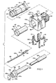
- In the drawings, Figure 1 is an enlarged perspective view of an electrical connector assembly of triaxial configuration and with parts in exploded configuration.
- Figure 2 is an enlarged fragmentary perspective view of a PCB, and further illustrating the parts shown in Figure 1 assembled to form an electrical connector assembly.
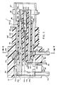
- Figure 3 is an enlarged longitudinal section view of the assembly shown in Figure 2.
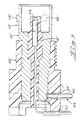
- Figure 4 is an enlarged cross section view of the assembly shown in Figure 2, and taken generally along the line 4-4 of Figure 3.
- Figure 5 is an enlarged longitudinal section view of an electrical connector assembly of coaxial configuration.
- Figures 1 through 4 of the drawings show an
electrical connector assembly 100. Aninsulative body 102 of theassembly 100 is fabricated, for example, by moulding a polymeric plastics material, and includes a hollowrectangular portion 103 that is integral with a hollowcylindrical portion 104.External threads 105 are on thecylindrical portion 104 for establishing a threaded connection to a panel, not shown. Thebody 102 has a cylindrical hollowinterior portion 106 extending axially through anopen end 107 of thecylindrical portion 104 and through anopen end 108 of therectangular portion 103. A radially projectinginterior shoulder 109 on thebody 102 faces toward theopen end 107 of thecylindrical portion 104. A radially inclined projecting interior shoulder 110 faces toward theopen end 108 of therectangular portion 103. - One
exterior wall 111 of therectangular portion 103 provides a base having projectingfeet 112 for standing against a PCB 113. A pair of spaced apartopenings wall 111 and theinterior portion 106. - The
assembly 100 further includes a triaxialelectrical connector 115 having a hollow andconductive exterior shell 116 of stepped cylindrical form for assembly by insertion into theopen end 107 of thecylindrical portion 104 of thebody 102. Theexterior shell 116 has adisconnect coupling portion 117 provided withbayonet coupling prongs 118 for disconnect coupling with a complementary electrical connector, not shown. Theexterior shell 116 further has an exterior and radially projectingshoulder 119 engaged against theend 107 and a second exterior radially projectingshoulder 120 engaged against theinterior shoulder 109 to limit the extent of insertion into the body 2. A flat recess 120ʹ in theexterior shell 116 intercepts theshoulder 120. - As shown in Figure 1, a
rear end 121 of theshell 116 is of reduced cylindrical thickness and projects axially from an internalcylindrical shoulder 122 at the junction of the reduced thickness with the increased thickness of the remainder of theshell 116. As shown in Figure 3, therear end 121 is flared after insertion in thebody 102 to form a radially outwardly flared lip engaged against the inclined shoulder 110 to prevent axial movement of theshell 116 toward theopen end 107 of thecylindrical portion 4. Arecess 123 of groove form encircles the cylindrical exterior of theshell 116 and is located along theshell 116 between theflared end 121 and theshoulder 120. Theinsulative body 102 holds theshell 116 in position within the hollowinterior portion 106 of the body, with thereccess 123 positioned in alignment with acorresponding opening 114. - The
assembly 100 includes a hollow cylindricalinsulative liner 124 for theshell 116. Theliner 124 is assembled by insertion into theopen end 108 of theinsulative body 102 and into theflared end 121 of theshell 116. Arear end 125 of theliner 124 has a radially projectingexternal flange 126 that covers theflared end 121 of theshell 116, and has a radially outward projectingexternal shoulder 127 adjacent theflange 126 that engages theinterior shoulder 122 of theshell 116 to limit insertion of theliner 124. - As shown in Figures 1 through 3, the
assembly 100 further includes a conductiveelectrical disconnect contact 128 formed by stamping a metal strip. Thedisconnect contact 128 has adisconnect contact portion 129 for disconnect connection with a known complementary electrical connector, not shown. Thedisconnect contact portion 129 is in the form of a hollow cylindrical electrical receptacle formed by bending the strip into a hollow cylindrical shape. Thedisconnect contact 128 has anelongated portion 130 in the plane of the strip and havingtapered wedge barbs electrical terminal 132 at the end of the strip formed by bending elongate edges of the strip out of the plane of the strip to form an elongated tube. As shown in Figures 1 and 3, thedisconnect contact 128 is inserted concentrically into anopen front end 133 of ahollow interior 134 of a cylindricaldielectric body 135. Thedisconnect contact portion 128 engages a radially projectingshoulder 136 of acylindrical portion 137 of theinterior 134, to limit insertion. Theshoulder 136 is at an intersection with apassage 138 along which is disposed theelongated portions contact 128. Thebarbs disconnect contact 128 from theinterior 134. Theelectrical terminal 132 of the contact projects outwardly of thedielectric body 135 for insertion into anaperture 139 of thePCB 113. - The
dielectric body 135 is inserted concentrically into anopen front end 140 of a conductiveintermediate shell 141. Thefront end 140 provides a disconnect connection to a complementary electrical connector, not shown. Ahollow interior 142 of theintermediate shell 141 has a radially projectingshoulder 143 that engages an external radially outward projectingshoulder 144 on thedielectric body 135 to limit insertion. Theintermediate shell 141 is assembled by insertion concentrically into therear end 125 of theinsulative liner 124. Arear end 145 of theintermediate shell 141 has an external radially projectingflange 146 of stepped diameter. An end of theflange 146 seats against therear end 125 of theinsulative liner 124.Portion 146a of theflange 146 spans theinterior 106 and provides a conductive barrier and electrical shield. Theinsulative body 104 holds theintermediate shell 141 in position within the hollowinterior portion 106 of thebody 104. The exterior of theflange 146 is provided with anexternal recess 147 that encircles the exterior of theflange 146 and is positioned due to assembly with thebody 104 in alignment with acorresponding opening 114. Following insertion of theintermediate shell 141, theterminal 132 of thecontact 128 is bent as shown in Figures 6 and 8 to project along achannel 148 that extends through theend 108 transversely of the axis of thedielectric body 102 and through thebase 111. Similarly, the terminal 32 is bent to project along achannel 148a that extends laterally of the axis of theintermediate shell 141 and that communicates with theinterior 142. Figures 1 and 3 show therear end 145 having a cylindrical recess 145a communicating with thechannel 148a. A thinconductive cap 145b initially of bulbous form is inserted into the recess 145a and its bulbous form is flattened by the application of pressure thereon causing thecap 145b to expand radially and span the recess 145a and frictionally engage the side of the recess to be retained in place and electrically shield theterminal 132. - Figures 1, 2 and 4 show a pair of
contacts respective openings contact contact 149 is perpendicular to its length and thickness. The strip form clip is curved along its length and transversely of its thickness to provide anarcuate holder 150 with anopen side 151 of a length less than the diameter of the remainder of theholder 150. Elongatedelectrical terminals resilient springs open side 151. Theholder 150 includes an outwardly projecting bight 153ʹ spaced equally between and along theholder 150 from thesprings spring Tab latching portions terminals terminals Ends terminals contact 149 to form edges of the channels. The ends 155, 155 are constructed for insertion intocorresponding apertures PCB 113, and resilient spring energy residing in theterminals terminals apertures PCB 113 with solder not shown. - Figure 4 shows the construction of a
corresponding opening 114 into which acontact 149 is inserted to establish an electrical connection with theouter shell 116. Theopening 114 communicates with thebase 111 and has an interior 156 of rectangular cross section with a width that slidably receives and confines the width of acorresponding contact 149. Thecontact 149 is inserted in theopening 114 and moved toward theshell 116, with theopen side 151 of theholder 150 facing theshell 116. Theterminals springs interior 156 of theopening 114 hasclearance spaces corresponding springs terminals holder 150 to the latchingprotions clearance spaces springs open side 151 of theholder 150 is lengthened in response to passage ofexterior shell 116 through theopen side 151 and into the confines of theholder 150. After passage of the exterior shell 16, thesprings shell 116 in opposite directions, and to close theholder 150 frictionally in engagement on the exterior of theshell 116. The bight 153ʹ remains outwardly spaced from theshell 116. The resilient spring energy urges theterminals interior 114. The latchingportions clearance spaces -
Interior shoulder clearance spaces interior 156. The latchingportions respective terminals respective shoulders corresponding contact 149 in thecorresponding opening 114 and resist removal of thecontact 149 from theopening 114. Theclearance spaces corresponding passageways body 102 and serving as access for a tool blade, not shown, for deflection of the latchingportions shoulders contact 149 from theinterior 156 of theopening 114 and allows withdrawal of thecontact 149 from theopening 114. - Figure 4 shows the
recess 123 with a diameter conforming to the arcuate shape of acorresponding holder 150. Therecess 123 has a width to receive and conform to the width of theholder 150. Figure 3 shows theintermediate shell 141 and theexterior shell 116 withcorresponding recesses insulative body 102 similarly with respect to correspondingopenings respective contacts - The
terminals connector 115 in a common direction and are arranged in a pattern wherein the terminal 132 is surrounded or circumscribed by an spaced equidistant from theother terminals terminal 132, or in the form of electrical interference that would interfere with electrical signals transmitted along the circumscribedterminal 132. - The
PCB 113 includes first and secondparallel surfaces 113a and 113b. Theapertures PCB 113 and communicate with thesurfaces 113a and 113b. Conductive means are in the form of elongatedelectrical circuit paths surface 113b. The conductive means 113c, 113c, 113c, 113c, 113c, 113cʹ, 113cʹ join corresponding additional conductive means 113d, 113d, 113d, 113d, 113d in the form of conductive walls lining the correspondingapertures first aperture 139 is constructed to receive theelectrical terminal 132 of thecontact 128. Theapertures terminals external shell 116, and theapertures terminals intermediate shell 141. Theapertures first aperture 139 is surrounded or circumscribed by theother apertures conductive walls conductive wall 113d of the circumscribedaperture 139 or from the terminal 132, or in the form of electrical interference that interferes, or would interfere, with the electrical signals transmitted along thewall 113d of the circumscribedaperture 139 or along theterminal 132. - Figure 5 illustrates an electrical connector assembly 1ʹ including an insulative body 2ʹ and a coaxial electrical connector 15ʹ. The coaxial connector 15ʹ includes the same disconnect contact 28 as the triaxial connector 15, and a conductive exterior shell 16ʹ similar to the shell 16, with bayonet prongs 18ʹ, 18ʹ. An insulative body 41ʹ concentrically surrounds the disconnect contact 28 and, in turn is concentrically surrounded by the exterior shell 16ʹ. A corresponding contact 49 of the type disclosed previously is inserted into a corresponding opening 14ʹ of the body 2ʹ and engages the exterior shell 16ʹ in a recess 23ʹ similar to the recess 23 of the shell 16.
- Although preferred embodiments have been described and shown, other embodiments and modifications are intended to be covered by the spirit and scope of the claims.
Claims (10)
the conductive contact (149) includes a holder (150) having an open side (148) for passage of the exterior shell (116, 116ʹ) into the holder (150), the conductive contact (149) includes conductive terminals (152, 152) extending from the holder (150) and extending outwardly from the base (111), and the contact receiving opening (114) is a passage admitting the holder (150) and the terminals (152, 152) into the interior (106).
Applications Claiming Priority (4)
| Application Number | Priority Date | Filing Date | Title |
|---|---|---|---|
| US89596486A | 1986-08-12 | 1986-08-12 | |
| US895964 | 1986-08-12 | ||
| US6522 | 1987-01-23 | ||
| US07/006,522 US4741703A (en) | 1986-08-12 | 1987-01-23 | PCB mounted triaxial connector assembly |
Publications (2)
| Publication Number | Publication Date |
|---|---|
| EP0256697A1 true EP0256697A1 (en) | 1988-02-24 |
| EP0256697B1 EP0256697B1 (en) | 1992-06-10 |
Family
ID=26675737
Family Applications (1)
| Application Number | Title | Priority Date | Filing Date |
|---|---|---|---|
| EP87306628A Expired - Lifetime EP0256697B1 (en) | 1986-08-12 | 1987-07-28 | Pcb mounted triaxial connector assembly |
Country Status (6)
| Country | Link |
|---|---|
| US (1) | US4741703A (en) |
| EP (1) | EP0256697B1 (en) |
| JP (1) | JPS6348781A (en) |
| KR (1) | KR880003455A (en) |
| DE (1) | DE3779702T2 (en) |
| ES (1) | ES2031899T3 (en) |
Cited By (4)
| Publication number | Priority date | Publication date | Assignee | Title |
|---|---|---|---|---|
| WO1990009686A1 (en) * | 1989-02-15 | 1990-08-23 | W.L. Gore & Associates, Inc. | Shielded right angled header |
| EP0547979A1 (en) * | 1991-12-18 | 1993-06-23 | RADIALL Société anonyme dite: | Coaxial connector for connecting two printed circuit boards |
| EP0867978A2 (en) * | 1997-03-27 | 1998-09-30 | Siemens Aktiengesellschaft | Angled coaxial connector |
| WO2000033423A1 (en) * | 1998-12-02 | 2000-06-08 | Nokia Networks Oy | Electrical connectors |
Families Citing this family (23)
| Publication number | Priority date | Publication date | Assignee | Title |
|---|---|---|---|---|
| FR2629953B1 (en) * | 1988-04-06 | 1991-07-05 | Sagem | ELECTRICAL COMPONENT, ESPECIALLY ELECTRIC MOTOR, EQUIPPED WITH DOUBLE PAIRS OF CONTACTS, PARTICULARLY FOR ALLOWING TWO DIFFERENT LOCATIONS ON A PRINTED CIRCUIT PLATE |
| US4884982A (en) * | 1989-04-03 | 1989-12-05 | Amp Incorporated | Capacitive coupled connector |
| US4975065A (en) * | 1989-09-26 | 1990-12-04 | Avantek, Inc. | Microwave circuit module connector |
| US5062811A (en) * | 1990-10-30 | 1991-11-05 | Amp Incorporated | Capacitive coupled connector for PCB grounding |
| US5088937A (en) * | 1991-04-19 | 1992-02-18 | Amp Incorporated | Right angle coaxial jack connector |
| US5112249A (en) * | 1991-10-18 | 1992-05-12 | Amp Incorporated | Connector locking clip |
| NL9200272A (en) * | 1992-02-14 | 1993-09-01 | Du Pont Nederland | COAX CONNECTOR MODULE FOR MOUNTING ON A PRINTED WIRING PLATE. |
| US5215470A (en) * | 1992-06-26 | 1993-06-01 | Amp Incorporated | Connector assembly and method of manufacture |
| US5437562A (en) * | 1993-03-26 | 1995-08-01 | The Whitaker Corporation | Low profile edge mount connector |
| US5482477A (en) * | 1994-06-28 | 1996-01-09 | The Whitaker Corporation | Micro-miniature coaxial connector with positive locking member |
| US5630720A (en) * | 1995-03-28 | 1997-05-20 | The Whitaker Corporation | Self polarizing electrical contact |
| CN1104067C (en) * | 1997-04-17 | 2003-03-26 | 三星电子株式会社 | Cable connector and monitor equipped with the same |
| US6273736B1 (en) * | 1997-07-22 | 2001-08-14 | Applied Materials, Inc. | Safety guard for an RF connector |
| DE19753839C1 (en) * | 1997-12-04 | 1999-04-29 | Siemens Ag | For coaxial angle plug-type connection unit |
| US6012931A (en) * | 1998-07-02 | 2000-01-11 | Berg Technology, Inc. | Connector having surface mount terminals for connecting to a printed circuit board |
| DE10048505A1 (en) * | 2000-09-29 | 2002-04-11 | Reitter & Schefenacker Gmbh | Plug connection device, preferably for exterior mirror of motor vehicles |
| US6863547B2 (en) * | 2003-05-01 | 2005-03-08 | Averatec Asia Incorporation | Method for suppressing electromagnetic interference of electronic device and electronic device with suppressed electromagnetic interference by the method |
| US6932614B1 (en) * | 2004-04-13 | 2005-08-23 | Shin-Nan Kan | Socket with double functions |
| US6994564B1 (en) * | 2004-10-13 | 2006-02-07 | Shin-Nan Kan | Connector having dual functions |
| CN101035408A (en) * | 2006-03-09 | 2007-09-12 | 鸿富锦精密工业(深圳)有限公司 | Circuit board |
| US7690922B2 (en) * | 2008-09-04 | 2010-04-06 | Chung-Chuan Huang | Electrical connector |
| JP5756608B2 (en) * | 2010-07-15 | 2015-07-29 | 矢崎総業株式会社 | connector |
| DE102016109266A1 (en) * | 2016-05-06 | 2017-11-09 | Rosenberger Hochfrequenztechnik Gmbh & Co. Kg | Plug connection device with at least one connector |
Citations (2)
| Publication number | Priority date | Publication date | Assignee | Title |
|---|---|---|---|---|
| US3493916A (en) * | 1967-07-24 | 1970-02-03 | Molex Products Co | Printed circuit board terminal and connector |
| US3514737A (en) * | 1968-02-21 | 1970-05-26 | Amp Inc | Printed circuit board socket connector |
Family Cites Families (11)
| Publication number | Priority date | Publication date | Assignee | Title |
|---|---|---|---|---|
| US3148010A (en) * | 1962-04-20 | 1964-09-08 | United Carr Inc | Test jack for printed circuit boards |
| US3121583A (en) * | 1962-10-26 | 1964-02-18 | Carl A Damm | Connector aligning device |
| FR2243578B1 (en) * | 1973-09-12 | 1976-11-19 | Honeywell Bull Soc Ind | |
| US4060887A (en) * | 1975-05-27 | 1977-12-06 | N. V. Raychem S.A. | Multiple conductor connector and method of connecting conductors to terminals therewith |
| JPS52107385A (en) * | 1976-03-03 | 1977-09-08 | Naado Kenkiyuushiyo Kk | Method printing gloves |
| CA1078038A (en) * | 1976-11-22 | 1980-05-20 | Richard C. Holt | Electrical interconnection boards with lead sockets mounted therein and method for making same |
| US4598970A (en) * | 1983-03-10 | 1986-07-08 | Hosiden Electronics Co., Ltd. | Internally split type jack |
| US4548453A (en) * | 1983-03-11 | 1985-10-22 | Amp Incorporated | Right angle coaxial plug connector |
| US4598961A (en) * | 1983-10-03 | 1986-07-08 | Amp Incorporated | Coaxial jack connector |
| US4609242A (en) * | 1984-11-06 | 1986-09-02 | Adc Telecommunications, Inc. | Electrical connector apparatus |
| US4659156A (en) * | 1985-06-24 | 1987-04-21 | Amp Incorporated | Coaxial connector with circuit board mounting features |
-
1987
- 1987-01-23 US US07/006,522 patent/US4741703A/en not_active Expired - Fee Related
- 1987-07-28 ES ES198787306628T patent/ES2031899T3/en not_active Expired - Lifetime
- 1987-07-28 EP EP87306628A patent/EP0256697B1/en not_active Expired - Lifetime
- 1987-07-28 DE DE8787306628T patent/DE3779702T2/en not_active Expired - Fee Related
- 1987-08-11 KR KR1019870008792A patent/KR880003455A/en not_active Application Discontinuation
- 1987-08-12 JP JP62201663A patent/JPS6348781A/en active Granted
Patent Citations (2)
| Publication number | Priority date | Publication date | Assignee | Title |
|---|---|---|---|---|
| US3493916A (en) * | 1967-07-24 | 1970-02-03 | Molex Products Co | Printed circuit board terminal and connector |
| US3514737A (en) * | 1968-02-21 | 1970-05-26 | Amp Inc | Printed circuit board socket connector |
Cited By (7)
| Publication number | Priority date | Publication date | Assignee | Title |
|---|---|---|---|---|
| WO1990009686A1 (en) * | 1989-02-15 | 1990-08-23 | W.L. Gore & Associates, Inc. | Shielded right angled header |
| EP0547979A1 (en) * | 1991-12-18 | 1993-06-23 | RADIALL Société anonyme dite: | Coaxial connector for connecting two printed circuit boards |
| FR2685553A1 (en) * | 1991-12-18 | 1993-06-25 | Radiall Sa | COAXIAL CONNECTOR ELEMENT ELBOW FIXED TO A PRINTED BOARD. |
| US5344340A (en) * | 1991-12-18 | 1994-09-06 | Radiall | Coaxial connector for connecting two printed-circuit boards |
| EP0867978A2 (en) * | 1997-03-27 | 1998-09-30 | Siemens Aktiengesellschaft | Angled coaxial connector |
| EP0867978A3 (en) * | 1997-03-27 | 1999-06-16 | Siemens Aktiengesellschaft | Angled coaxial connector |
| WO2000033423A1 (en) * | 1998-12-02 | 2000-06-08 | Nokia Networks Oy | Electrical connectors |
Also Published As
| Publication number | Publication date |
|---|---|
| DE3779702T2 (en) | 1993-01-28 |
| US4741703A (en) | 1988-05-03 |
| KR880003455A (en) | 1988-05-17 |
| JPH0584639B2 (en) | 1993-12-02 |
| JPS6348781A (en) | 1988-03-01 |
| DE3779702D1 (en) | 1992-07-16 |
| EP0256697B1 (en) | 1992-06-10 |
| ES2031899T3 (en) | 1993-01-01 |
Similar Documents
| Publication | Publication Date | Title |
|---|---|---|
| EP0256697B1 (en) | Pcb mounted triaxial connector assembly | |
| EP0208888B1 (en) | Snap-in terminal with wire guide | |
| JP2607881Y2 (en) | Power port terminal | |
| EP0294419B1 (en) | Low profile press fit connector | |
| US5322453A (en) | RF connector jack and plug assembly | |
| JPH0531824Y2 (en) | ||
| US6139363A (en) | Micro connector assembly and method of making the same | |
| US6056602A (en) | Electrical jack | |
| EP0780933A2 (en) | Electrical connector for circuit board | |
| US5112249A (en) | Connector locking clip | |
| US6929512B2 (en) | Cable end connector assembly with a shield device | |
| EP0794596B1 (en) | Connector module, connector module kit and connector module and panel assembly | |
| KR20000034964A (en) | Coaxial connector with switch | |
| EP0207306B1 (en) | Tab redundant terminal | |
| JPH07192819A (en) | Coaxial connector | |
| US6162103A (en) | Terminal structure of a connector | |
| JPH10284174A (en) | Connector with latch and latch for connector | |
| US6086419A (en) | Electrical connector assembly | |
| EP0207309B1 (en) | Folded redundant terminal | |
| CN114207950B (en) | Electrical plug connector | |
| US6447335B1 (en) | Cable end connector | |
| US6305979B1 (en) | Lower profile micro connector assembly | |
| US6322401B2 (en) | Electrical connector having contact orientation features | |
| US5672076A (en) | Shielded connector | |
| US7044804B2 (en) | Optical-electric connector |
Legal Events
| Date | Code | Title | Description |
|---|---|---|---|
| PUAI | Public reference made under article 153(3) epc to a published international application that has entered the european phase |
Free format text: ORIGINAL CODE: 0009012 |
|
| AK | Designated contracting states |
Kind code of ref document: A1 Designated state(s): DE ES FR GB IT NL |
|
| 17P | Request for examination filed |
Effective date: 19880721 |
|
| RAP3 | Party data changed (applicant data changed or rights of an application transferred) |
Owner name: AMP INCORPORATED (A NEW JERSEY CORPORATION) |
|
| RAP1 | Party data changed (applicant data changed or rights of an application transferred) |
Owner name: AMP INCORPORATED |
|
| 17Q | First examination report despatched |
Effective date: 19910130 |
|
| GRAA | (expected) grant |
Free format text: ORIGINAL CODE: 0009210 |
|
| AK | Designated contracting states |
Kind code of ref document: B1 Designated state(s): DE ES FR GB IT NL |
|
| REF | Corresponds to: |
Ref document number: 3779702 Country of ref document: DE Date of ref document: 19920716 |
|
| ITTA | It: last paid annual fee | ||
| ET | Fr: translation filed | ||
| ITF | It: translation for a ep patent filed |
Owner name: GUZZI E RAVIZZA S.R.L. |
|
| REG | Reference to a national code |
Ref country code: ES Ref legal event code: FG2A Ref document number: 2031899 Country of ref document: ES Kind code of ref document: T3 |
|
| PLBE | No opposition filed within time limit |
Free format text: ORIGINAL CODE: 0009261 |
|
| STAA | Information on the status of an ep patent application or granted ep patent |
Free format text: STATUS: NO OPPOSITION FILED WITHIN TIME LIMIT |
|
| 26N | No opposition filed | ||
| REG | Reference to a national code |
Ref country code: GB Ref legal event code: 732E |
|
| PGFP | Annual fee paid to national office [announced via postgrant information from national office to epo] |
Ref country code: ES Payment date: 19950714 Year of fee payment: 9 |
|
| PGFP | Annual fee paid to national office [announced via postgrant information from national office to epo] |
Ref country code: GB Payment date: 19960617 Year of fee payment: 10 |
|
| PGFP | Annual fee paid to national office [announced via postgrant information from national office to epo] |
Ref country code: FR Payment date: 19960715 Year of fee payment: 10 |
|
| PG25 | Lapsed in a contracting state [announced via postgrant information from national office to epo] |
Ref country code: ES Free format text: LAPSE BECAUSE OF EXPIRATION OF PROTECTION Effective date: 19960729 |
|
| PGFP | Annual fee paid to national office [announced via postgrant information from national office to epo] |
Ref country code: DE Payment date: 19960730 Year of fee payment: 10 |
|
| PG25 | Lapsed in a contracting state [announced via postgrant information from national office to epo] |
Ref country code: GB Free format text: LAPSE BECAUSE OF NON-PAYMENT OF DUE FEES Effective date: 19970728 |
|
| GBPC | Gb: european patent ceased through non-payment of renewal fee |
Effective date: 19970728 |
|
| PG25 | Lapsed in a contracting state [announced via postgrant information from national office to epo] |
Ref country code: FR Free format text: LAPSE BECAUSE OF NON-PAYMENT OF DUE FEES Effective date: 19980331 |
|
| PG25 | Lapsed in a contracting state [announced via postgrant information from national office to epo] |
Ref country code: DE Free format text: LAPSE BECAUSE OF NON-PAYMENT OF DUE FEES Effective date: 19980401 |
|
| REG | Reference to a national code |
Ref country code: FR Ref legal event code: ST |
|
| PGFP | Annual fee paid to national office [announced via postgrant information from national office to epo] |
Ref country code: NL Payment date: 19990630 Year of fee payment: 13 |
|
| REG | Reference to a national code |
Ref country code: ES Ref legal event code: FD2A Effective date: 19990601 |
|
| PG25 | Lapsed in a contracting state [announced via postgrant information from national office to epo] |
Ref country code: NL Free format text: LAPSE BECAUSE OF NON-PAYMENT OF DUE FEES Effective date: 20010201 |
|
| NLV4 | Nl: lapsed or anulled due to non-payment of the annual fee |
Effective date: 20010201 |
|
| PG25 | Lapsed in a contracting state [announced via postgrant information from national office to epo] |
Ref country code: IT Free format text: LAPSE BECAUSE OF NON-PAYMENT OF DUE FEES;WARNING: LAPSES OF ITALIAN PATENTS WITH EFFECTIVE DATE BEFORE 2007 MAY HAVE OCCURRED AT ANY TIME BEFORE 2007. THE CORRECT EFFECTIVE DATE MAY BE DIFFERENT FROM THE ONE RECORDED. Effective date: 20050728 |