EP0254844A2 - Digital pipelined heterodyne circuit - Google Patents
Digital pipelined heterodyne circuit Download PDFInfo
- Publication number
- EP0254844A2 EP0254844A2 EP87108201A EP87108201A EP0254844A2 EP 0254844 A2 EP0254844 A2 EP 0254844A2 EP 87108201 A EP87108201 A EP 87108201A EP 87108201 A EP87108201 A EP 87108201A EP 0254844 A2 EP0254844 A2 EP 0254844A2
- Authority
- EP
- European Patent Office
- Prior art keywords
- digital
- bit
- stage
- sine
- arithmetic
- Prior art date
- Legal status (The legal status is an assumption and is not a legal conclusion. Google has not performed a legal analysis and makes no representation as to the accuracy of the status listed.)
- Granted
Links
Images
Classifications
-
- H—ELECTRICITY
- H03—ELECTRONIC CIRCUITRY
- H03D—DEMODULATION OR TRANSFERENCE OF MODULATION FROM ONE CARRIER TO ANOTHER
- H03D7/00—Transference of modulation from one carrier to another, e.g. frequency-changing
-
- H—ELECTRICITY
- H03—ELECTRONIC CIRCUITRY
- H03D—DEMODULATION OR TRANSFERENCE OF MODULATION FROM ONE CARRIER TO ANOTHER
- H03D2200/00—Indexing scheme relating to details of demodulation or transference of modulation from one carrier to another covered by H03D
- H03D2200/0041—Functional aspects of demodulators
- H03D2200/0054—Digital filters
- H03D2200/0056—Digital filters including a digital decimation filter
-
- H—ELECTRICITY
- H03—ELECTRONIC CIRCUITRY
- H03D—DEMODULATION OR TRANSFERENCE OF MODULATION FROM ONE CARRIER TO ANOTHER
- H03D2200/00—Indexing scheme relating to details of demodulation or transference of modulation from one carrier to another covered by H03D
- H03D2200/0041—Functional aspects of demodulators
- H03D2200/0066—Mixing
- H03D2200/0072—Mixing by complex multiplication
Definitions
- the present invention relates to a digital pipelined heterodyne circuit for heterodyning a data input signal by a signal of a predetermined frequency.
- Heterodyning is a technique that has application in many areas of communiations and signal processing. For example, in spectrum analysis, it is often necessary to shift the center frequency of a broad-band signal into a region where a narrow-band filter may be located which is used to sample input data.
- digital heterodyne circuits are available which digitize a data input signal and multiply that signal by the sine and cosine components of a user-chosen reference signal having a predetermined frequency. The problem with such circuits is that each data byte must be digitally multiplied by digital sine and cosine coefficients one at a time.
- Digital multiplication is a two-step process involving the combining of one bit of the sine and cosine coefficient with the data byte in an AND-gate array and then adding the product to the previous product formed by the previous gate array. It will take as many steps to completely multiply the data byte as there are bits in the sine and cosine coefficients. For example, if there are m significant bits, each data input byte must be processed, one bit at a time, m times, before the next byte can be processed. This leads to unacceptably slow processing time, especially if high resolution is required.
- the present invention provides a digital heterodyne circuit which includes a data input line for providing a sequence of digitized data signals and digital sine and cosine function generators for generating m-bit digital coefficients as a function of time at a predetermined frequency.
- An m-stage digital multiplier is provided for multiplying the digitized data signals by the coefficients generated by the sine and cosine function generators.
- Time delay circuits are connected between the function generators and the m-stage multiplier for providing each bit of each digital coefficient to each respective stage of the multiplier means simultaneously with the arrival at each such stage of a predetermined digitized data signal.
- This circuit provides a pipelined heterodyne circuit in which data input bytes are sequentially processed such that each time a data byte enters a particular stage for partial multiplication, the previous data byte is being processed downstream in the next stage.
- a unique shift register makes available an additional bit of digital sine and cosine coefficients that were generated when the byte first entered the data input. This is made possible by a unique triangular shift register in which the number of stages of the shift register connecting each bit output of the sine and cosine function generators with each respective stage of the multiplier includes the same number of stages as the rank in significance of the particular bit.
- the most significant bit output of the sine and cosine function generators include a one-stage shift register.
- the second most significant bit includes a two-stage shift register, and so on, up to an m-stage shift register connecting the mth significant bit with the m th multiplication stage.
- This circuit provides an increase in speed over conventional digital heterodyne circuits by a factor of m where m is the number of significant bits produced by the sine and cosine function generators.
- the output is filtered in a low-pass decimation filter.
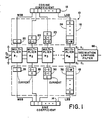
- a digital heterodyne circuit l0 includes a cosine coefficient generator l2 and a sine coefficient generator l4.
- Cosine coefficient generator l2 is connected to a triangular shift register l6, and sine coefficient generator l4 is connected to a similar triangular shift register l8.
- Each of the triangular shift registers l6 and l8 comprise a number of individual single-stage or multi-stage shift registers for each bit output of respective cosine and sine coefficient generators l2 and l4.
- the most significant bit output of cosine coefficient generator l2 is connected to a single-stage shift register 20, while the next two significant bits of cosine coefficient generator l2 are connected to two-stage shift register 22 and three-stage shift register 23.
- the least significant bit of the cosine coefficient generator l2 is connected to an m stage shift register 24.
- the connections between the sine coefficient generator l4 and triangular shift register l8 are the same as those described with respect to cosine coefficient generator l2.
- the most significant bit of sine coefficient generator l4 is connected to single-stage shift register 26.
- the next most significant bit of sine coefficient generator l4 is connected to two-stage shift register 28, as is the next most significant bit connected to three-stage shift register 30.
- the least significant bit of sine coefficient generator l4 is connected to m-stage shift register 32.
- a digitized data signal Di enters on data input line 34 where it is multiplied in multiplier l by the output of the most significant bit shift registers 20 and 26 respectively. If the data signal at multiplier l is arbitrarily designated as the current data input, it can be seen that the current digital cosine and sine coefficients, which are labelled with the letter "c", are loaded into the triangular shift registers l6 and l8, respectively. This happens each time a new data input signal Di is provided to multiplier l.
- a system clock (not shown) clocks a data byte into multiplier l and simultaneously enables the cosine and sine function generators l2 and l4 to generate a new m-bit coefficient to be loaded into shift registers l6 and l8, respectively.
- the cosine and sine coefficient generators l2 and l4 load a digital coefficient representing the sine function and cosine functions respectively of an angle ⁇ t which varies with time where ⁇ is a predetermined frequency chosen by the user.
- the previous data input signal Downstream from multiplier l, in multiplier 2, the previous data input signal is simultaneously processed by the previous cosine and sine coefficients labelled c-l, and in the m th multiplier stage, multiplier m, the m th previous data input signal is being processed by the c-m cosine and sine coefficients, respectively.
- a data input signal enters the "pipeline" at multiplier l, it will be partially multiplied in each of the multipliers by a bit generated by cosine coefficient generator l2 and sine coefficient generator l4 of sine and cosine coefficients respectively that were generated at the particular time that the data signal was clocked into multiplier l.
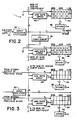
- multiplier l is a digital multipler includes an input register 36 which is connected to data input line 34.
- the input register 36 is connected to a 2's complement generator 38 which simultaneously provides the 2's complement of each data byte stored in the input register 36 to AND gate arrays 40 and 42, respectively.
- the n bits of the output of 2's complement generator 38 are provided to a set of parallel AND gates which are all combined with the most significant bit of the sine and cosine coefficients, respectively.
- the 2's complement of each data input signal is used for this purpose in order to properly maintain the word length of the data input signals which may change in polarity from plus to minus.
- the outputs of AND gate arrays 40 and 42, respectively, are provided to adders 44 and 46, respectively, which add the input data signal multiplied by the most significant bit of the cosine and sine coefficients, respectively to an n-bit ground signal.
- the sum of these two numbers is stored in storage registers 48 and 50, respectively.
- multiplier stages are shown in FIG. 3. For each such stage, an input line from the stored output of the previous stage is provided to adders 52 and 54, respectively.
- the k th most significant bits of the cosine and sine coefficient generators l2 and l4 are provided to AND gate arrays 56 and 58, respectively. This bit is combined with the input data signal held in input register 60.
- the output of AND gate arrays 56 and 58 are added to the stored output of the previous stage in adders 53 and 54, and the results are stored in storage registers 62 and 64, respectively.
- multiplier M passes the outputs of its storage registers, which are now the product of digitized input signal D i and a sine and cosine coefficient labelled S i and C i , respectively, to a decimation low-pass filter 66 for the purpose of removing transient noise.
Abstract
Description
- The present invention relates to a digital pipelined heterodyne circuit for heterodyning a data input signal by a signal of a predetermined frequency.
- Heterodyning is a technique that has application in many areas of communiations and signal processing. For example, in spectrum analysis, it is often necessary to shift the center frequency of a broad-band signal into a region where a narrow-band filter may be located which is used to sample input data. In order to accomplish this function, digital heterodyne circuits are available which digitize a data input signal and multiply that signal by the sine and cosine components of a user-chosen reference signal having a predetermined frequency. The problem with such circuits is that each data byte must be digitally multiplied by digital sine and cosine coefficients one at a time. Digital multiplication is a two-step process involving the combining of one bit of the sine and cosine coefficient with the data byte in an AND-gate array and then adding the product to the previous product formed by the previous gate array. It will take as many steps to completely multiply the data byte as there are bits in the sine and cosine coefficients. For example, if there are m significant bits, each data input byte must be processed, one bit at a time, m times, before the next byte can be processed. This leads to unacceptably slow processing time, especially if high resolution is required.
- The present invention provides a digital heterodyne circuit which includes a data input line for providing a sequence of digitized data signals and digital sine and cosine function generators for generating m-bit digital coefficients as a function of time at a predetermined frequency. An m-stage digital multiplier is provided for multiplying the digitized data signals by the coefficients generated by the sine and cosine function generators. Time delay circuits are connected between the function generators and the m-stage multiplier for providing each bit of each digital coefficient to each respective stage of the multiplier means simultaneously with the arrival at each such stage of a predetermined digitized data signal.
- This circuit provides a pipelined heterodyne circuit in which data input bytes are sequentially processed such that each time a data byte enters a particular stage for partial multiplication, the previous data byte is being processed downstream in the next stage. As each data byte proceeds sequentially from one stage to the next, a unique shift register makes available an additional bit of digital sine and cosine coefficients that were generated when the byte first entered the data input. This is made possible by a unique triangular shift register in which the number of stages of the shift register connecting each bit output of the sine and cosine function generators with each respective stage of the multiplier includes the same number of stages as the rank in significance of the particular bit. Thus, the most significant bit output of the sine and cosine function generators include a one-stage shift register. The second most significant bit includes a two-stage shift register, and so on, up to an m-stage shift register connecting the mth significant bit with the mth multiplication stage. This circuit provides an increase in speed over conventional digital heterodyne circuits by a factor of m where m is the number of significant bits produced by the sine and cosine function generators. The output is filtered in a low-pass decimation filter.
- It is a principal object of this invention to provide a digital pipelined heterodyne circuit for increasing the speed of digitally heterodyning an input data signal with a signal of a given frequency.
-
- FIG. l is a block schematic diagram of the digital heterodyne circuit of the present invention.
- FIG. 2 is a block schematic diagram of multiplier stage number l shown in FIG. l.
- FIG. 3 is a block schematic diagram of a circuit utilized in
multiplier stages 2 through m in FIG. l. - A digital heterodyne circuit l0 includes a cosine coefficient generator l2 and a sine coefficient generator l4. Cosine coefficient generator l2 is connected to a triangular shift register l6, and sine coefficient generator l4 is connected to a similar triangular shift register l8. Each of the triangular shift registers l6 and l8 comprise a number of individual single-stage or multi-stage shift registers for each bit output of respective cosine and sine coefficient generators l2 and l4. For example, the most significant bit output of cosine coefficient generator l2 is connected to a single-
stage shift register 20, while the next two significant bits of cosine coefficient generator l2 are connected to two-stage shift register 22 and three-stage shift register 23. The least significant bit of the cosine coefficient generator l2 is connected to an mstage shift register 24. The connections between the sine coefficient generator l4 and triangular shift register l8 are the same as those described with respect to cosine coefficient generator l2. The most significant bit of sine coefficient generator l4 is connected to single-stage shift register 26. The next most significant bit of sine coefficient generator l4 is connected to two-stage shift register 28, as is the next most significant bit connected to three-stage shift register 30. The least significant bit of sine coefficient generator l4 is connected to m-stage shift register 32. - A digitized data signal Di enters on
data input line 34 where it is multiplied in multiplier l by the output of the most significantbit shift registers - Downstream from multiplier l, in
multiplier 2, the previous data input signal is simultaneously processed by the previous cosine and sine coefficients labelled c-l, and in the mth multiplier stage, multiplier m, the mth previous data input signal is being processed by the c-m cosine and sine coefficients, respectively. Thus, as a data input signal enters the "pipeline" at multiplier l, it will be partially multiplied in each of the multipliers by a bit generated by cosine coefficient generator l2 and sine coefficient generator l4 of sine and cosine coefficients respectively that were generated at the particular time that the data signal was clocked into multiplier l. Simultaneously, other data signals are multiplied by different bits of different sine and cosine coefficients that were generated at earlier times. In this way, as a data input signal progresses through each of the multiplier stages, being partially multiplied each time by one bit of the same sine and cosine coefficients, other data signals are being simultaneously processed in other multiplier stages by partial multiplication using the appropriately generated bits of the sine and cosine coefficients. This speeds up the multiplication process by a factor of m. - Referring to FIG. 2, multiplier l is a digital multipler includes an
input register 36 which is connected todata input line 34. Theinput register 36 is connected to a 2's complement generator 38 which simultaneously provides the 2's complement of each data byte stored in theinput register 36 toAND gate arrays 's complement generator 38 are provided to a set of parallel AND gates which are all combined with the most significant bit of the sine and cosine coefficients, respectively. The 2's complement of each data input signal is used for this purpose in order to properly maintain the word length of the data input signals which may change in polarity from plus to minus. The outputs ofAND gate arrays storage registers - The following multiplier stages are shown in FIG. 3. For each such stage, an input line from the stored output of the previous stage is provided to adders 52 and 54, respectively. The kth most significant bits of the cosine and sine coefficient generators l2 and l4 are provided to
AND gate arrays input register 60. The output ofAND gate arrays adders 53 and 54, and the results are stored instorage registers - Referring again to FIG. l, the last multiplier stage, labelled multiplier M in FIG. l, passes the outputs of its storage registers, which are now the product of digitized input signal Di and a sine and cosine coefficient labelled Si and Ci, respectively, to a decimation low-
pass filter 66 for the purpose of removing transient noise. - The terms and expressions which have been employed in the foregoing specification are used therein as terms of descrip tion and not of limitation, and there is no intention, in the use of such terms and expressions, of excluding equivalents of the features shown and described or portions thereof, it being recognized that the scope of the invention is defined and limited only by the claims which follow.
Claims (9)
Applications Claiming Priority (2)
| Application Number | Priority Date | Filing Date | Title |
|---|---|---|---|
| US06/890,192 US4791600A (en) | 1986-07-28 | 1986-07-28 | Digital pipelined heterodyne circuit |
| US890192 | 1986-07-28 |
Publications (3)
| Publication Number | Publication Date |
|---|---|
| EP0254844A2 true EP0254844A2 (en) | 1988-02-03 |
| EP0254844A3 EP0254844A3 (en) | 1988-12-14 |
| EP0254844B1 EP0254844B1 (en) | 1990-11-14 |
Family
ID=25396368
Family Applications (1)
| Application Number | Title | Priority Date | Filing Date |
|---|---|---|---|
| EP87108201A Expired - Lifetime EP0254844B1 (en) | 1986-07-28 | 1987-06-05 | Digital pipelined heterodyne circuit |
Country Status (4)
| Country | Link |
|---|---|
| US (1) | US4791600A (en) |
| EP (1) | EP0254844B1 (en) |
| JP (1) | JPS6337741A (en) |
| DE (1) | DE3766179D1 (en) |
Cited By (28)
| Publication number | Priority date | Publication date | Assignee | Title |
|---|---|---|---|---|
| EP0632577A1 (en) * | 1993-07-02 | 1995-01-04 | Ford Motor Company | Multi-stage digital RF translator |
| US6256358B1 (en) | 1998-03-27 | 2001-07-03 | Visteon Global Technologies, Inc. | Digital signal processing architecture for multi-band radio receiver |
| WO2001071906A2 (en) * | 2000-03-22 | 2001-09-27 | Parkervision, Inc. | Integrated frequency translation and selectivity with gain control functionality, and applications thereof |
| US6560301B1 (en) | 1998-10-21 | 2003-05-06 | Parkervision, Inc. | Integrated frequency translation and selectivity with a variety of filter embodiments |
| US6634555B1 (en) | 2000-01-24 | 2003-10-21 | Parker Vision, Inc. | Bar code scanner using universal frequency translation technology for up-conversion and down-conversion |
| US6647250B1 (en) | 1998-10-21 | 2003-11-11 | Parkervision, Inc. | Method and system for ensuring reception of a communications signal |
| US6687493B1 (en) | 1998-10-21 | 2004-02-03 | Parkervision, Inc. | Method and circuit for down-converting a signal using a complementary FET structure for improved dynamic range |
| US6694128B1 (en) | 1998-08-18 | 2004-02-17 | Parkervision, Inc. | Frequency synthesizer using universal frequency translation technology |
| US6704558B1 (en) | 1999-01-22 | 2004-03-09 | Parkervision, Inc. | Image-reject down-converter and embodiments thereof, such as the family radio service |
| US6704549B1 (en) | 1999-03-03 | 2004-03-09 | Parkvision, Inc. | Multi-mode, multi-band communication system |
| US6748220B1 (en) | 2000-05-05 | 2004-06-08 | Nortel Networks Limited | Resource allocation in wireless networks |
| US6783069B1 (en) | 1999-12-06 | 2004-08-31 | Xerox Corporation | Method and apparatus for implementing a camera mouse |
| US6798351B1 (en) | 1998-10-21 | 2004-09-28 | Parkervision, Inc. | Automated meter reader applications of universal frequency translation |
| US6813485B2 (en) | 1998-10-21 | 2004-11-02 | Parkervision, Inc. | Method and system for down-converting and up-converting an electromagnetic signal, and transforms for same |
| US7653158B2 (en) | 2001-11-09 | 2010-01-26 | Parkervision, Inc. | Gain control in a communication channel |
| US7653145B2 (en) | 1999-08-04 | 2010-01-26 | Parkervision, Inc. | Wireless local area network (WLAN) using universal frequency translation technology including multi-phase embodiments and circuit implementations |
| US7693230B2 (en) | 1999-04-16 | 2010-04-06 | Parkervision, Inc. | Apparatus and method of differential IQ frequency up-conversion |
| US7724845B2 (en) | 1999-04-16 | 2010-05-25 | Parkervision, Inc. | Method and system for down-converting and electromagnetic signal, and transforms for same |
| US7773688B2 (en) | 1999-04-16 | 2010-08-10 | Parkervision, Inc. | Method, system, and apparatus for balanced frequency up-conversion, including circuitry to directly couple the outputs of multiple transistors |
| US7822401B2 (en) | 2000-04-14 | 2010-10-26 | Parkervision, Inc. | Apparatus and method for down-converting electromagnetic signals by controlled charging and discharging of a capacitor |
| US7865177B2 (en) | 1998-10-21 | 2011-01-04 | Parkervision, Inc. | Method and system for down-converting an electromagnetic signal, and transforms for same, and aperture relationships |
| US7894789B2 (en) | 1999-04-16 | 2011-02-22 | Parkervision, Inc. | Down-conversion of an electromagnetic signal with feedback control |
| US7991815B2 (en) | 2000-11-14 | 2011-08-02 | Parkervision, Inc. | Methods, systems, and computer program products for parallel correlation and applications thereof |
| US8019291B2 (en) | 1998-10-21 | 2011-09-13 | Parkervision, Inc. | Method and system for frequency down-conversion and frequency up-conversion |
| US8160196B2 (en) | 2002-07-18 | 2012-04-17 | Parkervision, Inc. | Networking methods and systems |
| US8233855B2 (en) | 1998-10-21 | 2012-07-31 | Parkervision, Inc. | Up-conversion based on gated information signal |
| US8295406B1 (en) | 1999-08-04 | 2012-10-23 | Parkervision, Inc. | Universal platform module for a plurality of communication protocols |
| US8407061B2 (en) | 2002-07-18 | 2013-03-26 | Parkervision, Inc. | Networking methods and systems |
Families Citing this family (2)
| Publication number | Priority date | Publication date | Assignee | Title |
|---|---|---|---|---|
| US6477214B1 (en) | 1999-02-04 | 2002-11-05 | Lockheed Martin Corporation | Phase-based frequency estimation using filter banks |
| US20040073690A1 (en) * | 2002-09-30 | 2004-04-15 | Neil Hepworth | Voice over IP endpoint call admission |
Citations (2)
| Publication number | Priority date | Publication date | Assignee | Title |
|---|---|---|---|---|
| US3956622A (en) * | 1974-12-20 | 1976-05-11 | Bell Telephone Laboratories, Incorporated | Two's complement pipeline multiplier |
| EP0035166A1 (en) * | 1980-03-01 | 1981-09-09 | Licentia Patent-Verwaltungs-GmbH | Digital receiver |
Family Cites Families (7)
| Publication number | Priority date | Publication date | Assignee | Title |
|---|---|---|---|---|
| FR2409652A1 (en) * | 1977-11-18 | 1979-06-15 | Materiel Telephonique | MULTI-FREQUENCY CODED DIGITAL SIGNAL RECEIVER |
| JPS5731043A (en) * | 1980-07-31 | 1982-02-19 | Toshiba Corp | Semiconductor operating circuit |
| JPS5932216A (en) * | 1982-08-17 | 1984-02-21 | Sony Corp | Digital signal processing circuit and digital filter |
| JPS59196629A (en) * | 1983-04-21 | 1984-11-08 | Nec Corp | Fm receiver |
| JPS59196657A (en) * | 1983-04-21 | 1984-11-08 | Nec Corp | Delay detecting circuit |
| GB2155669A (en) * | 1984-03-06 | 1985-09-25 | Sony Corp | Galois field multipliers |
| US4698769A (en) * | 1985-02-04 | 1987-10-06 | American Telephone And Telegraph Company | Supervisory audio tone detection in a radio channel |
-
1986
- 1986-07-28 US US06/890,192 patent/US4791600A/en not_active Expired - Fee Related
-
1987
- 1987-06-05 EP EP87108201A patent/EP0254844B1/en not_active Expired - Lifetime
- 1987-06-05 DE DE8787108201T patent/DE3766179D1/en not_active Expired - Fee Related
- 1987-07-28 JP JP62188679A patent/JPS6337741A/en active Pending
Patent Citations (2)
| Publication number | Priority date | Publication date | Assignee | Title |
|---|---|---|---|---|
| US3956622A (en) * | 1974-12-20 | 1976-05-11 | Bell Telephone Laboratories, Incorporated | Two's complement pipeline multiplier |
| EP0035166A1 (en) * | 1980-03-01 | 1981-09-09 | Licentia Patent-Verwaltungs-GmbH | Digital receiver |
Non-Patent Citations (1)
| Title |
|---|
| IEEE JOURNAL OF SOLID-STATE CIRCUITS, vol. SC-11, no. 5, October 1976, pages 669-678, IEEE, New York, US; J. KANE: "A low-power, bipolar, two's complement serial pipeline multiplier chip" * |
Cited By (49)
| Publication number | Priority date | Publication date | Assignee | Title |
|---|---|---|---|---|
| US5490173A (en) * | 1993-07-02 | 1996-02-06 | Ford Motor Company | Multi-stage digital RF translator |
| EP0632577A1 (en) * | 1993-07-02 | 1995-01-04 | Ford Motor Company | Multi-stage digital RF translator |
| US6256358B1 (en) | 1998-03-27 | 2001-07-03 | Visteon Global Technologies, Inc. | Digital signal processing architecture for multi-band radio receiver |
| US6694128B1 (en) | 1998-08-18 | 2004-02-17 | Parkervision, Inc. | Frequency synthesizer using universal frequency translation technology |
| US8233855B2 (en) | 1998-10-21 | 2012-07-31 | Parkervision, Inc. | Up-conversion based on gated information signal |
| US7936022B2 (en) | 1998-10-21 | 2011-05-03 | Parkervision, Inc. | Method and circuit for down-converting a signal |
| US8160534B2 (en) | 1998-10-21 | 2012-04-17 | Parkervision, Inc. | Applications of universal frequency translation |
| US6647250B1 (en) | 1998-10-21 | 2003-11-11 | Parkervision, Inc. | Method and system for ensuring reception of a communications signal |
| US6687493B1 (en) | 1998-10-21 | 2004-02-03 | Parkervision, Inc. | Method and circuit for down-converting a signal using a complementary FET structure for improved dynamic range |
| US6560301B1 (en) | 1998-10-21 | 2003-05-06 | Parkervision, Inc. | Integrated frequency translation and selectivity with a variety of filter embodiments |
| US8190108B2 (en) | 1998-10-21 | 2012-05-29 | Parkervision, Inc. | Method and system for frequency up-conversion |
| US8019291B2 (en) | 1998-10-21 | 2011-09-13 | Parkervision, Inc. | Method and system for frequency down-conversion and frequency up-conversion |
| US7937059B2 (en) | 1998-10-21 | 2011-05-03 | Parkervision, Inc. | Converting an electromagnetic signal via sub-sampling |
| US8190116B2 (en) | 1998-10-21 | 2012-05-29 | Parker Vision, Inc. | Methods and systems for down-converting a signal using a complementary transistor structure |
| US6798351B1 (en) | 1998-10-21 | 2004-09-28 | Parkervision, Inc. | Automated meter reader applications of universal frequency translation |
| US6813485B2 (en) | 1998-10-21 | 2004-11-02 | Parkervision, Inc. | Method and system for down-converting and up-converting an electromagnetic signal, and transforms for same |
| US6836650B2 (en) | 1998-10-21 | 2004-12-28 | Parkervision, Inc. | Methods and systems for down-converting electromagnetic signals, and applications thereof |
| US8340618B2 (en) | 1998-10-21 | 2012-12-25 | Parkervision, Inc. | Method and system for down-converting an electromagnetic signal, and transforms for same, and aperture relationships |
| US7865177B2 (en) | 1998-10-21 | 2011-01-04 | Parkervision, Inc. | Method and system for down-converting an electromagnetic signal, and transforms for same, and aperture relationships |
| US7693502B2 (en) | 1998-10-21 | 2010-04-06 | Parkervision, Inc. | Method and system for down-converting an electromagnetic signal, transforms for same, and aperture relationships |
| US7826817B2 (en) | 1998-10-21 | 2010-11-02 | Parker Vision, Inc. | Applications of universal frequency translation |
| US7697916B2 (en) | 1998-10-21 | 2010-04-13 | Parkervision, Inc. | Applications of universal frequency translation |
| US6704558B1 (en) | 1999-01-22 | 2004-03-09 | Parkervision, Inc. | Image-reject down-converter and embodiments thereof, such as the family radio service |
| US6704549B1 (en) | 1999-03-03 | 2004-03-09 | Parkvision, Inc. | Multi-mode, multi-band communication system |
| US8229023B2 (en) | 1999-04-16 | 2012-07-24 | Parkervision, Inc. | Wireless local area network (WLAN) using universal frequency translation technology including multi-phase embodiments |
| US8223898B2 (en) | 1999-04-16 | 2012-07-17 | Parkervision, Inc. | Method and system for down-converting an electromagnetic signal, and transforms for same |
| US7724845B2 (en) | 1999-04-16 | 2010-05-25 | Parkervision, Inc. | Method and system for down-converting and electromagnetic signal, and transforms for same |
| US7894789B2 (en) | 1999-04-16 | 2011-02-22 | Parkervision, Inc. | Down-conversion of an electromagnetic signal with feedback control |
| US8036304B2 (en) | 1999-04-16 | 2011-10-11 | Parkervision, Inc. | Apparatus and method of differential IQ frequency up-conversion |
| US7693230B2 (en) | 1999-04-16 | 2010-04-06 | Parkervision, Inc. | Apparatus and method of differential IQ frequency up-conversion |
| US8594228B2 (en) | 1999-04-16 | 2013-11-26 | Parkervision, Inc. | Apparatus and method of differential IQ frequency up-conversion |
| US8077797B2 (en) | 1999-04-16 | 2011-12-13 | Parkervision, Inc. | Method, system, and apparatus for balanced frequency up-conversion of a baseband signal |
| US7929638B2 (en) | 1999-04-16 | 2011-04-19 | Parkervision, Inc. | Wireless local area network (WLAN) using universal frequency translation technology including multi-phase embodiments |
| US7773688B2 (en) | 1999-04-16 | 2010-08-10 | Parkervision, Inc. | Method, system, and apparatus for balanced frequency up-conversion, including circuitry to directly couple the outputs of multiple transistors |
| US8224281B2 (en) | 1999-04-16 | 2012-07-17 | Parkervision, Inc. | Down-conversion of an electromagnetic signal with feedback control |
| US7653145B2 (en) | 1999-08-04 | 2010-01-26 | Parkervision, Inc. | Wireless local area network (WLAN) using universal frequency translation technology including multi-phase embodiments and circuit implementations |
| US8295406B1 (en) | 1999-08-04 | 2012-10-23 | Parkervision, Inc. | Universal platform module for a plurality of communication protocols |
| US6783069B1 (en) | 1999-12-06 | 2004-08-31 | Xerox Corporation | Method and apparatus for implementing a camera mouse |
| US6634555B1 (en) | 2000-01-24 | 2003-10-21 | Parker Vision, Inc. | Bar code scanner using universal frequency translation technology for up-conversion and down-conversion |
| WO2001071906A2 (en) * | 2000-03-22 | 2001-09-27 | Parkervision, Inc. | Integrated frequency translation and selectivity with gain control functionality, and applications thereof |
| WO2001071906A3 (en) * | 2000-03-22 | 2003-10-16 | Parkervision Inc | Integrated frequency translation and selectivity with gain control functionality, and applications thereof |
| US7822401B2 (en) | 2000-04-14 | 2010-10-26 | Parkervision, Inc. | Apparatus and method for down-converting electromagnetic signals by controlled charging and discharging of a capacitor |
| US8295800B2 (en) | 2000-04-14 | 2012-10-23 | Parkervision, Inc. | Apparatus and method for down-converting electromagnetic signals by controlled charging and discharging of a capacitor |
| US6748220B1 (en) | 2000-05-05 | 2004-06-08 | Nortel Networks Limited | Resource allocation in wireless networks |
| US7991815B2 (en) | 2000-11-14 | 2011-08-02 | Parkervision, Inc. | Methods, systems, and computer program products for parallel correlation and applications thereof |
| US7653158B2 (en) | 2001-11-09 | 2010-01-26 | Parkervision, Inc. | Gain control in a communication channel |
| US8446994B2 (en) | 2001-11-09 | 2013-05-21 | Parkervision, Inc. | Gain control in a communication channel |
| US8160196B2 (en) | 2002-07-18 | 2012-04-17 | Parkervision, Inc. | Networking methods and systems |
| US8407061B2 (en) | 2002-07-18 | 2013-03-26 | Parkervision, Inc. | Networking methods and systems |
Also Published As
| Publication number | Publication date |
|---|---|
| JPS6337741A (en) | 1988-02-18 |
| EP0254844A3 (en) | 1988-12-14 |
| EP0254844B1 (en) | 1990-11-14 |
| DE3766179D1 (en) | 1990-12-20 |
| US4791600A (en) | 1988-12-13 |
Similar Documents
| Publication | Publication Date | Title |
|---|---|---|
| US4791600A (en) | Digital pipelined heterodyne circuit | |
| US4736335A (en) | Multiplier-accumulator circuit using latched sums and carries | |
| JP2777207B2 (en) | Reconfigurable multiprocessor | |
| EP0102784B1 (en) | Method and apparatus for sine function generation | |
| Freeny | Special-purpose hardware for digital filtering | |
| EP0080836A2 (en) | Monolithic discrete-time digital convolution circuit | |
| EP0146963A2 (en) | Iir digital filter | |
| US4802111A (en) | Cascadable digital filter processor employing moving coefficients | |
| US4563750A (en) | Fast Fourier transform apparatus with data timing schedule decoupling | |
| US5694347A (en) | Digital signal processing system | |
| EP0442356A2 (en) | Weighted-delay column adder and method of organizing same | |
| US3721812A (en) | Fast fourier transform computer and method for simultaneously processing two independent sets of data | |
| EP0238300B1 (en) | Serial digital signal processing circuitry | |
| EP0517241A2 (en) | Interleaved multiplier accumulator | |
| JPH0831776B2 (en) | Digital filter | |
| JP3082394B2 (en) | Multi-channel decimation filter for sigma-delta analog-to-digital converter | |
| JPH10509011A (en) | Improved digital filter | |
| US4041297A (en) | Real-time multiplier with selectable number of product digits | |
| JP2825255B2 (en) | Semiconductor integrated circuit device | |
| Williams | An expandable single-IC digital filter/correlator | |
| US6324222B1 (en) | Digital receiver with polyphase structure | |
| Dadda | Byte-serial convolvers | |
| KR0136484B1 (en) | Parallel multiplier | |
| Cappellini et al. | A special-purpose online processor for bandpass analysis | |
| Farazian et al. | Programmable Digital Baud Integrators for the Radar High-Speed Data Acquisition System |
Legal Events
| Date | Code | Title | Description |
|---|---|---|---|
| PUAI | Public reference made under article 153(3) epc to a published international application that has entered the european phase |
Free format text: ORIGINAL CODE: 0009012 |
|
| AK | Designated contracting states |
Kind code of ref document: A2 Designated state(s): DE FR GB NL |
|
| PUAL | Search report despatched |
Free format text: ORIGINAL CODE: 0009013 |
|
| AK | Designated contracting states |
Kind code of ref document: A3 Designated state(s): DE FR GB NL |
|
| 17P | Request for examination filed |
Effective date: 19890314 |
|
| 17Q | First examination report despatched |
Effective date: 19890623 |
|
| GRAA | (expected) grant |
Free format text: ORIGINAL CODE: 0009210 |
|
| AK | Designated contracting states |
Kind code of ref document: B1 Designated state(s): DE FR GB NL |
|
| REF | Corresponds to: |
Ref document number: 3766179 Country of ref document: DE Date of ref document: 19901220 |
|
| ET | Fr: translation filed | ||
| PG25 | Lapsed in a contracting state [announced via postgrant information from national office to epo] |
Ref country code: GB Effective date: 19910605 |
|
| PLBE | No opposition filed within time limit |
Free format text: ORIGINAL CODE: 0009261 |
|
| STAA | Information on the status of an ep patent application or granted ep patent |
Free format text: STATUS: NO OPPOSITION FILED WITHIN TIME LIMIT |
|
| 26N | No opposition filed | ||
| PG25 | Lapsed in a contracting state [announced via postgrant information from national office to epo] |
Ref country code: NL Effective date: 19920101 |
|
| GBPC | Gb: european patent ceased through non-payment of renewal fee | ||
| NLV4 | Nl: lapsed or anulled due to non-payment of the annual fee | ||
| PG25 | Lapsed in a contracting state [announced via postgrant information from national office to epo] |
Ref country code: FR Effective date: 19920228 |
|
| PG25 | Lapsed in a contracting state [announced via postgrant information from national office to epo] |
Ref country code: DE Effective date: 19920401 |
|
| REG | Reference to a national code |
Ref country code: FR Ref legal event code: ST |