EP0253201A2 - Structure containing hydrogenated amorphous silicon and process - Google Patents
Structure containing hydrogenated amorphous silicon and process Download PDFInfo
- Publication number
- EP0253201A2 EP0253201A2 EP87109391A EP87109391A EP0253201A2 EP 0253201 A2 EP0253201 A2 EP 0253201A2 EP 87109391 A EP87109391 A EP 87109391A EP 87109391 A EP87109391 A EP 87109391A EP 0253201 A2 EP0253201 A2 EP 0253201A2
- Authority
- EP
- European Patent Office
- Prior art keywords
- layer
- amorphous silicon
- concentration
- hydrogen
- hydrogenated amorphous
- Prior art date
- Legal status (The legal status is an assumption and is not a legal conclusion. Google has not performed a legal analysis and makes no representation as to the accuracy of the status listed.)
- Granted
Links
- 229910021417 amorphous silicon Inorganic materials 0.000 title claims abstract description 69
- 238000000034 method Methods 0.000 title claims abstract description 22
- 239000001257 hydrogen Substances 0.000 claims abstract description 51
- 229910052739 hydrogen Inorganic materials 0.000 claims abstract description 51
- UFHFLCQGNIYNRP-UHFFFAOYSA-N Hydrogen Chemical compound [H][H] UFHFLCQGNIYNRP-UHFFFAOYSA-N 0.000 claims abstract description 49
- 239000000758 substrate Substances 0.000 claims abstract description 23
- KWYUFKZDYYNOTN-UHFFFAOYSA-M Potassium hydroxide Chemical compound [OH-].[K+] KWYUFKZDYYNOTN-UHFFFAOYSA-M 0.000 claims description 12
- 238000005530 etching Methods 0.000 claims description 12
- HEMHJVSKTPXQMS-UHFFFAOYSA-M Sodium hydroxide Chemical compound [OH-].[Na+] HEMHJVSKTPXQMS-UHFFFAOYSA-M 0.000 claims description 9
- 230000008021 deposition Effects 0.000 claims description 9
- 239000000243 solution Substances 0.000 claims description 8
- 239000012670 alkaline solution Substances 0.000 claims description 3
- 239000000463 material Substances 0.000 description 19
- 238000000151 deposition Methods 0.000 description 14
- 229920002120 photoresistant polymer Polymers 0.000 description 13
- 239000010409 thin film Substances 0.000 description 9
- 230000001965 increasing effect Effects 0.000 description 7
- VYPSYNLAJGMNEJ-UHFFFAOYSA-N Silicium dioxide Chemical compound O=[Si]=O VYPSYNLAJGMNEJ-UHFFFAOYSA-N 0.000 description 6
- 230000000694 effects Effects 0.000 description 6
- 230000005855 radiation Effects 0.000 description 6
- 239000002019 doping agent Substances 0.000 description 5
- 230000005669 field effect Effects 0.000 description 5
- 239000007789 gas Substances 0.000 description 5
- 239000000203 mixture Substances 0.000 description 5
- 238000001020 plasma etching Methods 0.000 description 5
- XKRFYHLGVUSROY-UHFFFAOYSA-N Argon Chemical compound [Ar] XKRFYHLGVUSROY-UHFFFAOYSA-N 0.000 description 4
- BLRPTPMANUNPDV-UHFFFAOYSA-N Silane Chemical compound [SiH4] BLRPTPMANUNPDV-UHFFFAOYSA-N 0.000 description 4
- XUIMIQQOPSSXEZ-UHFFFAOYSA-N Silicon Chemical compound [Si] XUIMIQQOPSSXEZ-UHFFFAOYSA-N 0.000 description 4
- 239000011521 glass Substances 0.000 description 4
- 238000003384 imaging method Methods 0.000 description 4
- 239000012212 insulator Substances 0.000 description 4
- 229910052751 metal Inorganic materials 0.000 description 4
- 239000002184 metal Substances 0.000 description 4
- 229910000077 silane Inorganic materials 0.000 description 4
- 229910052710 silicon Inorganic materials 0.000 description 4
- 239000010703 silicon Substances 0.000 description 4
- 235000012239 silicon dioxide Nutrition 0.000 description 4
- 238000003631 wet chemical etching Methods 0.000 description 4
- ZOXJGFHDIHLPTG-UHFFFAOYSA-N Boron Chemical group [B] ZOXJGFHDIHLPTG-UHFFFAOYSA-N 0.000 description 3
- XYFCBTPGUUZFHI-UHFFFAOYSA-N Phosphine Chemical compound P XYFCBTPGUUZFHI-UHFFFAOYSA-N 0.000 description 3
- 229910052796 boron Inorganic materials 0.000 description 3
- 239000004065 semiconductor Substances 0.000 description 3
- PXHVJJICTQNCMI-UHFFFAOYSA-N Nickel Chemical compound [Ni] PXHVJJICTQNCMI-UHFFFAOYSA-N 0.000 description 2
- 150000008044 alkali metal hydroxides Chemical class 0.000 description 2
- 229910052786 argon Inorganic materials 0.000 description 2
- 229910052799 carbon Inorganic materials 0.000 description 2
- 239000003085 diluting agent Substances 0.000 description 2
- 239000001307 helium Substances 0.000 description 2
- 229910052734 helium Inorganic materials 0.000 description 2
- SWQJXJOGLNCZEY-UHFFFAOYSA-N helium atom Chemical compound [He] SWQJXJOGLNCZEY-UHFFFAOYSA-N 0.000 description 2
- BHEPBYXIRTUNPN-UHFFFAOYSA-N hydridophosphorus(.) (triplet) Chemical group [PH] BHEPBYXIRTUNPN-UHFFFAOYSA-N 0.000 description 2
- 150000002431 hydrogen Chemical class 0.000 description 2
- 239000011261 inert gas Substances 0.000 description 2
- 229910052743 krypton Inorganic materials 0.000 description 2
- DNNSSWSSYDEUBZ-UHFFFAOYSA-N krypton atom Chemical compound [Kr] DNNSSWSSYDEUBZ-UHFFFAOYSA-N 0.000 description 2
- 229910052754 neon Inorganic materials 0.000 description 2
- GKAOGPIIYCISHV-UHFFFAOYSA-N neon atom Chemical compound [Ne] GKAOGPIIYCISHV-UHFFFAOYSA-N 0.000 description 2
- 238000000059 patterning Methods 0.000 description 2
- 239000010453 quartz Substances 0.000 description 2
- 229910052594 sapphire Inorganic materials 0.000 description 2
- 239000010980 sapphire Substances 0.000 description 2
- 239000000377 silicon dioxide Substances 0.000 description 2
- VYZAMTAEIAYCRO-UHFFFAOYSA-N Chromium Chemical compound [Cr] VYZAMTAEIAYCRO-UHFFFAOYSA-N 0.000 description 1
- ZOKXTWBITQBERF-UHFFFAOYSA-N Molybdenum Chemical compound [Mo] ZOKXTWBITQBERF-UHFFFAOYSA-N 0.000 description 1
- 229910052581 Si3N4 Inorganic materials 0.000 description 1
- 229910052782 aluminium Inorganic materials 0.000 description 1
- XAGFODPZIPBFFR-UHFFFAOYSA-N aluminium Chemical compound [Al] XAGFODPZIPBFFR-UHFFFAOYSA-N 0.000 description 1
- QVGXLLKOCUKJST-UHFFFAOYSA-N atomic oxygen Chemical compound [O] QVGXLLKOCUKJST-UHFFFAOYSA-N 0.000 description 1
- 238000005452 bending Methods 0.000 description 1
- 229910052804 chromium Inorganic materials 0.000 description 1
- 239000011651 chromium Substances 0.000 description 1
- 230000002301 combined effect Effects 0.000 description 1
- 150000001875 compounds Chemical class 0.000 description 1
- 239000013078 crystal Substances 0.000 description 1
- 229910021419 crystalline silicon Inorganic materials 0.000 description 1
- 238000010586 diagram Methods 0.000 description 1
- ZOCHARZZJNPSEU-UHFFFAOYSA-N diboron Chemical compound B#B ZOCHARZZJNPSEU-UHFFFAOYSA-N 0.000 description 1
- 238000009826 distribution Methods 0.000 description 1
- 238000001312 dry etching Methods 0.000 description 1
- 238000005538 encapsulation Methods 0.000 description 1
- 239000008246 gaseous mixture Substances 0.000 description 1
- 238000007654 immersion Methods 0.000 description 1
- 238000002329 infrared spectrum Methods 0.000 description 1
- 238000005224 laser annealing Methods 0.000 description 1
- 238000004519 manufacturing process Methods 0.000 description 1
- 238000005259 measurement Methods 0.000 description 1
- 239000007769 metal material Substances 0.000 description 1
- 238000001465 metallisation Methods 0.000 description 1
- 150000002739 metals Chemical class 0.000 description 1
- 229910052750 molybdenum Inorganic materials 0.000 description 1
- 239000011733 molybdenum Substances 0.000 description 1
- 229910000096 monohydride Inorganic materials 0.000 description 1
- 229910052759 nickel Inorganic materials 0.000 description 1
- 239000001301 oxygen Substances 0.000 description 1
- 229910052760 oxygen Inorganic materials 0.000 description 1
- 238000002161 passivation Methods 0.000 description 1
- 229910000073 phosphorus hydride Inorganic materials 0.000 description 1
- 229910021420 polycrystalline silicon Inorganic materials 0.000 description 1
- 229910021332 silicide Inorganic materials 0.000 description 1
- HQVNEWCFYHHQES-UHFFFAOYSA-N silicon nitride Chemical compound N12[Si]34N5[Si]62N3[Si]51N64 HQVNEWCFYHHQES-UHFFFAOYSA-N 0.000 description 1
- 230000002226 simultaneous effect Effects 0.000 description 1
- TXEYQDLBPFQVAA-UHFFFAOYSA-N tetrafluoromethane Chemical compound FC(F)(F)F TXEYQDLBPFQVAA-UHFFFAOYSA-N 0.000 description 1
Images

Classifications
-
- H—ELECTRICITY
- H01—ELECTRIC ELEMENTS
- H01L—SEMICONDUCTOR DEVICES NOT COVERED BY CLASS H10
- H01L29/00—Semiconductor devices adapted for rectifying, amplifying, oscillating or switching, or capacitors or resistors with at least one potential-jump barrier or surface barrier, e.g. PN junction depletion layer or carrier concentration layer; Details of semiconductor bodies or of electrodes thereof ; Multistep manufacturing processes therefor
- H01L29/66—Types of semiconductor device ; Multistep manufacturing processes therefor
- H01L29/68—Types of semiconductor device ; Multistep manufacturing processes therefor controllable by only the electric current supplied, or only the electric potential applied, to an electrode which does not carry the current to be rectified, amplified or switched
- H01L29/76—Unipolar devices, e.g. field effect transistors
- H01L29/772—Field effect transistors
- H01L29/78—Field effect transistors with field effect produced by an insulated gate
- H01L29/786—Thin film transistors, i.e. transistors with a channel being at least partly a thin film
- H01L29/78606—Thin film transistors, i.e. transistors with a channel being at least partly a thin film with supplementary region or layer in the thin film or in the insulated bulk substrate supporting it for controlling or increasing the safety of the device
- H01L29/78618—Thin film transistors, i.e. transistors with a channel being at least partly a thin film with supplementary region or layer in the thin film or in the insulated bulk substrate supporting it for controlling or increasing the safety of the device characterised by the drain or the source properties, e.g. the doping structure, the composition, the sectional shape or the contact structure
-
- H—ELECTRICITY
- H01—ELECTRIC ELEMENTS
- H01L—SEMICONDUCTOR DEVICES NOT COVERED BY CLASS H10
- H01L21/00—Processes or apparatus adapted for the manufacture or treatment of semiconductor or solid state devices or of parts thereof
- H01L21/02—Manufacture or treatment of semiconductor devices or of parts thereof
- H01L21/02104—Forming layers
- H01L21/02365—Forming inorganic semiconducting materials on a substrate
- H01L21/02367—Substrates
- H01L21/0237—Materials
-
- H—ELECTRICITY
- H01—ELECTRIC ELEMENTS
- H01L—SEMICONDUCTOR DEVICES NOT COVERED BY CLASS H10
- H01L21/00—Processes or apparatus adapted for the manufacture or treatment of semiconductor or solid state devices or of parts thereof
- H01L21/02—Manufacture or treatment of semiconductor devices or of parts thereof
- H01L21/02104—Forming layers
- H01L21/02365—Forming inorganic semiconducting materials on a substrate
- H01L21/02436—Intermediate layers between substrates and deposited layers
- H01L21/02439—Materials
- H01L21/02441—Group 14 semiconducting materials
- H01L21/0245—Silicon, silicon germanium, germanium
-
- H—ELECTRICITY
- H01—ELECTRIC ELEMENTS
- H01L—SEMICONDUCTOR DEVICES NOT COVERED BY CLASS H10
- H01L21/00—Processes or apparatus adapted for the manufacture or treatment of semiconductor or solid state devices or of parts thereof
- H01L21/02—Manufacture or treatment of semiconductor devices or of parts thereof
- H01L21/02104—Forming layers
- H01L21/02365—Forming inorganic semiconducting materials on a substrate
- H01L21/02518—Deposited layers
- H01L21/02521—Materials
- H01L21/02524—Group 14 semiconducting materials
- H01L21/02532—Silicon, silicon germanium, germanium
-
- H—ELECTRICITY
- H01—ELECTRIC ELEMENTS
- H01L—SEMICONDUCTOR DEVICES NOT COVERED BY CLASS H10
- H01L21/00—Processes or apparatus adapted for the manufacture or treatment of semiconductor or solid state devices or of parts thereof
- H01L21/02—Manufacture or treatment of semiconductor devices or of parts thereof
- H01L21/02104—Forming layers
- H01L21/02365—Forming inorganic semiconducting materials on a substrate
- H01L21/02612—Formation types
- H01L21/02617—Deposition types
- H01L21/0262—Reduction or decomposition of gaseous compounds, e.g. CVD
-
- H—ELECTRICITY
- H01—ELECTRIC ELEMENTS
- H01L—SEMICONDUCTOR DEVICES NOT COVERED BY CLASS H10
- H01L29/00—Semiconductor devices adapted for rectifying, amplifying, oscillating or switching, or capacitors or resistors with at least one potential-jump barrier or surface barrier, e.g. PN junction depletion layer or carrier concentration layer; Details of semiconductor bodies or of electrodes thereof ; Multistep manufacturing processes therefor
- H01L29/66—Types of semiconductor device ; Multistep manufacturing processes therefor
- H01L29/68—Types of semiconductor device ; Multistep manufacturing processes therefor controllable by only the electric current supplied, or only the electric potential applied, to an electrode which does not carry the current to be rectified, amplified or switched
- H01L29/76—Unipolar devices, e.g. field effect transistors
- H01L29/772—Field effect transistors
- H01L29/78—Field effect transistors with field effect produced by an insulated gate
- H01L29/786—Thin film transistors, i.e. transistors with a channel being at least partly a thin film
- H01L29/78651—Silicon transistors
- H01L29/7866—Non-monocrystalline silicon transistors
- H01L29/78663—Amorphous silicon transistors
- H01L29/78669—Amorphous silicon transistors with inverted-type structure, e.g. with bottom gate
Landscapes
- Engineering & Computer Science (AREA)
- Microelectronics & Electronic Packaging (AREA)
- Power Engineering (AREA)
- Condensed Matter Physics & Semiconductors (AREA)
- General Physics & Mathematics (AREA)
- Physics & Mathematics (AREA)
- Computer Hardware Design (AREA)
- Manufacturing & Machinery (AREA)
- Ceramic Engineering (AREA)
- Chemical & Material Sciences (AREA)
- Materials Engineering (AREA)
- Thin Film Transistor (AREA)
- Weting (AREA)
- Drying Of Semiconductors (AREA)
Abstract
Description
- The present invention is concerned with a structure for providing semiconductor devices and to a process for fabricating such. The present invention is especially applicable to structures that, in turn, are suitable for providing thin-film field effect transistors. The present invention provides a relatively simple and readily reproducible process for obtaining such structures.
- In obtaining semiconductur devices, it is often necessary to obtain a predetermined pattern of thicker and thinner layers of semiconductor material. Such pattern is generally more useful if the semiconductor material is a deposited thin film (as opposed to bulk grown crystal) material, for example, hydrogenated amorphous silicon, or crystalline silicon formed by the high temperature or laser annealing of the amorphous material. One particular application being thin-film field effect transistors.
- A typical thin-film field effect transistor includes an electrically conductive gate above an insulating substrate such as glass, a gate insulator such as silicon dioxide above the gate, a hydrogenated amorphous silicon layer above the gate insulator, an electrically conductive source and drain regions above the amorphous silicon. It is desired for such devices to control the current such that when the device is in the "on" state, as high a current as possible exists, but when the device is in the "off" state, the residual current is as small as possible. To achieve such it is desirable to provide doping in the amorphous silicon layer beneath the source and drain regions, but to limit the doping in the amorphous silicon layer in the region between the source and drain regions referred to as the "channel".
- Presently, such patterns are fabricated by plasma depositing a layer of uniform thickness hydrogenated amorphous silicon, protecting the desired thicker part of the pattern with a resist image, and etching the unprotected area for a predetermined length of time. However, in order to achieve a well-defined remaining thickness in the etched areas, meticulous control of conditions and of timing is required. Such is relatively expensive and often not practical to implement. Accordingly, these methods are not very well developed and not convenient from a manufacturing or commercial viewpoint.
- The present invention is concerned with a structure and process capable of providing a pattern multilevel structure that is relatively simple and readily reproducible. In particular, the structure of the present invention includes a substrate (1) that has at least one major surface area. Above the major surface area of the substrate is a first layer (4) of hydrogenated amorphous silicon. The first layer of hydrogenated amorphous silicon contains a first concentration of hydrogen incorporated therein. Located above the first layer of hydrogenated amorphous silicon is a second layer (5) of hydrogenated amorphous silicon. The second layer of hydrogenated amorphous silicon has a second concentration of hydrogen incorporated therein that differs from the concentration of hydrogen incorporated in the first layer.
- In addition, the present invention is concerned with a process for fabricating a structure. The process includes providing a substrate (1) having at least one major surface area. Above the major surface area of the substrate is provided a first layer (4) of hydrogenated amorphous silicon. The first layer of hydrogenated amorphous silicon has a first concentration of hydrogen incorporated therein. A second layer (5) of hydrogenated amorphous silicon is provided above the first layer. This second layer has a second concentration of hydrogen incorporated therein that differs from the concentration of hydrogen incorporated in the first layer. A vertically differentiated pattern is provided by selectively etching the layer of hydrogenated amorphous silicon having the higher hydrogen concentration of the first and second layers.
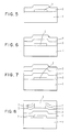
- Figures 1 to 4 are schematic diagrams showing the structure in various stages of processing in accordance with the present invention.
- Figures 5 to 8 illustrate the application of the invention in fabricating thin film field effect transistors.
- In Figure 1 is illustrated a substrate (1).
- The substrate (1) includes any suitable substrate material such as glass (e.g., quartz), sapphire, silicon, metal, or metallized substrate.
- A first layer (4) of hydrogenated amorphous silicon containing a first concentration of hydrogen incorporated therein is deposited (see Figure 2). In the preferred aspects of the present invention, hydrogenated amorphous silicon layer (4) contains a relatively low concentration of hydrogen as compared to the subsequently to be applied hydrogenated amorphous silicon layer (5). The hydrogenated amorphous silicon layer (4) can be provided by well-known plasma deposition techniques such as placing the structure in a plasma reaction chamber using silane as the source of the hydrogenated amorphous silicon. For the lower concentration of hydrogen, it is preferred to use temperatures of about 225°C to about 325°C and most preferably about 275°C and at a pressure of about 20 µbar (15 millitorr) to about 1.33 mbar (1 torr) and most preferably about 306µbar (230 millitorr). A typical power density is about 5 milliwatts/cm² of combined surface area of the electrodes exposed to the plasma. The power source is typically operated at a radio frequency of about 13.6 megahertz.
- Although the preferred source of the hydrogenated amorphous silicon is 100% silane, such, if desired, can be diluted with an inert gas such as helium, neon, argon, and krypton or diluted with hydrogen. It is known that the presence of hydrogen in the diluent gas will not significantly effect the amount of hydrogen deposited along with the silicon in the hydrogenated amorphous silicon layer.
- Moreover, other methods for depositing the hydrogenated amorphous silicon such as those disclosed in U.S. Patent 4,363,828 can be employed if desired.
- Next, the second layer (5) of hydrogenated amorphous silicon is deposited (see Figure 3). In the preferred aspects of the present invention the second layer of hydrogenated amorphous silicon (5) contains the greater quantity of hydrogen of the two layers. The increased quantity of incorporated hydrogen can be achieved by the same plasma deposition employed for the first hydrogenated amorphous silicon layer, except by employing a reduced temperature and/or increased pressure. In the preferred aspects of the present invention, the temperature employed for the second hydrogenated amorphous silicon layer is reduced to about room temperature to about 200°C and preferably about 125°C while employing the same pressure as used for depositing the first hydrogenated amorphous silicon layer (4).
- The thicknesses of the two layers may be chosen at will within the limits of practicality of thin films depositions. Important benefits of the present invention as compared to the prior art will, however, derive when the second layer is thicker or not much thinner than the first layer and when both layers are relatively thin. Thus, typical thicknesses of the first hydrogenated amorphous silicon layer (4) are about 10 to about 5,000 nm and preferably about 10 to about 100 nm.
- Typical thicknesses of hydrogenated amorphous silicon layer (5) are about 5 to about 5,000 nm and preferably about 10 to about 100 nm.
- The higher concentration of hydrogen in the second hydrogenated amorphous silicon layer results in that layer being more rapidly etched, thereby making it possible to accurately etch down to the interface with first hydrogenated layer (4) allowing for a well-defined remaining thickness as well as a flat surface.
- Accordingly, the second hydrogenated amorphous silicon layer (5) can be patterned (see Figure 4), for instance, by covering the layer (5) with a photoresist material (not shown) exposing the photoresist material to imaging radiation in a predetermined pattern and, thereafter, removing that portion of the photoresist material exposed to the imaging radiation in the case of a positive photoresist material and that material not exposed to radiation in the case of a negative photoresist material as is well-known in the art.
- Next, the portion of the second hydrogenated amorphous silicon layer (5) no longer protected by photoresist material is exposed to a suitable etchant in order to develop the desired pattern in the layer (4). Suitable wet chemical etching compositions include strongly alkaline solutions such as alkali metal hydroxide solutions and, in particular, potassium hydroxide and sodium hydroxide. Such compositions preferably are 1 molar or higher. The etching is preferably carried out at normal room temperatures. When more elevated temperatures are employed, the pH of the solution can be somewhat less than that obtained from a 1 molar solution, such as down to about 12.5. Moreover, if desired, other methods of etching can be employed, although not preferred, such as plasma etching or reactive ion etching. The most pronounced effects from the present invention are achieved when employing a wet chemical etching.
- In view of the fact that the second layer (5) has the higher hydrogen content and, therefore, etches more rapidly than the first layer, the etching can be carried out such that the etch rate will slow down as the interface to layer (4) is reached, thereby allowing a well-defined remaining thickness and a planar surface.
- The level of hydrogen in hydrogenated layers (4) and (5) can now be equilibrated once layer (5) has been patterned by merely raising the temperature of the substrate to that at which the first layer was formed, such as at about 225°C to about 325°C and preferably at about 275°C and maintain the substrate there for a sufficient amount of time in order to lower the hydrogen content in the second layer. This usually takes about 1 to about 30 minutes.
- Reference to Figures 5 to 8 illustrates the application of the present invention in fabricating thin film effect transistors.
- In Figure 5 is illustrated a substrate (1) containing an electrically conductive gate (2) thereon and a gate insulator (3).
- The substrate (1) includes any suitable substrate material such as glass (e.g., quartz), sapphire, silicon, metal, or metallized substrate.
- The gate (2) is of a metallic-type high electrical conductivity material, preferably a metal such as chromium, nickel, molybdenum and aluminum, as well as non-metallic materials such as highly doped polycrystalline silicon or intermetallic silicides which, nevertheless, have electrical conductivities of the magnitude generally possessed by metals. The gate (2) is defined by well-known photolithographical techniques that need not be discussed herein in any detail.
- Electrically insulating gate (2) is a gate insulator (3) such as silicon dioxide and silicon nitride.
- A first layer (4) of hydrogenated amorphous silicon containing a first concentration of hydrogen incorporated therein is deposited (see Figure 6). In the preferred aspects of the present invention, hydrogenated amorphous silicon layer (4) contains a relatively low concentration of hydrogen as compared to the subsequently to be applied hydrogenated amorphous silicon layer (5). The hydrogenated amorphous silicon layer (4) can be provided by well-known plasma deposition techniques such as placing the structure in a plasma reaction chamber using silane as the source of the hydrogenated amorphous silicon. For the lower concentration of hydrogen, it is preferred to use temperatures of about 225°C to about 325°C and most preferably about 275°C and at a pressure of about 20 µbar (15 millitorr) to about 1.33 mbar (1 torr) and most preferably about 306 µbar (230 millitorr). A typical power density is about 5 milliwatts/cm² of combined surface area of the electrodes exposed to the plasma. The power source is typically operated at a radio frequency of about 13.6 megahertz.
- Although the preferred source of the hydrogenated amorphous silicon is 100% silane, such, if desired, can be diluted with an inert gas such as helium, neon, argon, and krypton or diluted with hydrogen. It is known that the presence of hydrogen in the diluent gas will not significantly effect the amount of hydrogen deposited along with the silicon in the hydrogenated amorphous silicon layer.
- Moreover, other methods for depositing the hydrogenated amorphous silicon such as those disclosed in U.S. Patent 4,363,828 can be employed if desired.
- Next, the second layer (5) of hydrogenated amorphous silicon is deposited (see Figure 3). In the preferred aspects of the present invention the second layer of hydrogenated amorphous silicon (5) contains the greater quantity of hydrogen of the two layers. The increased quantity of incorporated hydrogen can be achieved by the same plasma deposition employed for the first hydrogenated amorphous silicon layer, except by employing a reduced temperature and/or increased pressure. In the preferred aspects of the present invention, the temperature employed for the second hydrogenated amorphous silicon layer is reduced to about room temperature to about 200°C and preferably about 125°C while employing the same pressure as used for depositing the first hydrogenated amorphous silicon layer (4).
- As discussed above, the thickness of the two layers may be chosen at will within the limits of practicality of thin films depositions. Important benefits of the present invention as compared to the prior art will, however, derive when the second layer is thicker or not much thinner than the first layer and when both layers are relatively thin. Thus, typical thicknesses of the first hydrogenated amorphous silicon layer (4) are about 10 to about 5,000 nm and preferably about 10 to about 100 nm.
- Typical thicknesses of hydrogenated amorphous silicon layer (5) are about 5 to about 5,000 nm and preferably about 10 to about 100 nm.
- In addition, for the preferred aspects of the present invention, when the present invention is to be used to provide a thin-film field effect transistor, the second hydrogenated amorphous silicon layer is also doped in order to increase its conductivity. A suitable n-type dopant is phosphorous and a suitable p-type dopant is boron. The phosphorous can be incorporated, for instance, by including in the plasma gas, phosphine (PH₃), such as in amounts of a few ppm to about 1% by volume of the gaseous mixture employed. The boron can be provided by using a gaseous boron-containing compound such as diborane (B₂H₆).
- The higher concentration of hydrogen in the second hydrogenated amorphous silicon layer results in that layer being more rapidly etched, thereby making it possible to accurately etch down to the interface with first hydrogenated layer (4) allowing for a well-defined remaining thickness as well as a flat surface.
- Accordingly, the second hydrogenated amorphous silicon layer (5) can be patterned (see Figure 4), for instance, by covering the layer (5) with a photoresist material (not shown) exposing the photoresist material to imaging radiation in a predetermined pattern and, thereafter, removing that portion of the photoresist material exposed to the imaging radiation in the case of a positive photoresist material and that material not exposed to radiation in the case of a negative photoresist material as is well-known in the art.
- Next, the portion of the second hydrogenated amorphous silicon layer (5) no longer protected by photoresist material is exposed to a suitable etchant in order to develop the desired pattern in the layer (4). Suitable wet chemical etching compositions include strongly alkaline solutions such as alkali metal hydroxide solutions and, in particular, potassium hydroxide and sodium hydroxide. Such compositions preferably are 1 molar or higher. The etching is preferably carried out at normal room temperatures. When more elevated temperatures are employed, the pH of the solution can be somewhat less than that obtained from a 1 molar solution, such as down to about 12.5. Moreover, if desired, other methods of etching can be employed, although not preferred, such as plasma etching or reactive ion etching. The most pronounced effects from the present invention are achieved when employing a wet chemical etching.
- In view of the fact that the second layer (5) has the higher hydrogen content and, therefore, etches more rapidly than the first layer, the etching can be carried out such that the etch rate will slow down as the interface to layer (4) is reached, thereby allowing a well-defined remaining thickness and a planar surface.
- That portion of layer (5) that remains is patterned so as to beneath source and drain regions to be subsequently provided, while that portion of layer (5) removed corresponds to the area between the source and drain regions to be provided, referred to as the "channel". Accordingly, by proper doping of layer (5), increased conductivity beneath the source and drain regions can be obtained without concomitantly increasing the conductivity between the source and drain regions when the device is in the "off" state. This, in turn, allows for improved ohmic contact. In other words, increased ohmic contact is provided by the doping between the hydrogenated amorphous silicon and the source and drain regions, but the highly doped amorphous layer is cleanly removed from the channel region between the source and drain regions. Source and drain regions (7) and (8) are provided by well-known techniques, for examples, by depositing a blanket metallization (not shown) prior to application of the photoresist on top of layer (5) and patterning it with the mask as used for patterning layer (5).
- The level of hydrogen in hydrogenated layers (4) and (5) can be equilibrated once layer (5) has been patterned by merely raising the temperature of the substrate to that at which the first layer was formed, such as at about 225°C to about 325°C and preferably at about 275°C and maintain the substrate there for a sufficient amount of time in order to lower the hydrogen content in the second layer. This usually takes about 1 to about 30 minutes.
- Depending on application, the etched region can be covered with a passivation or encapsulation layer (6).
- Although the present invention has been described with respect to only two different layers of hydrogenated amorphous silicon, it is understood that the present invention can be carried out with three or more different layers or thicknesses of hydrogenated amorphous silicon, each having a different concentration of hydrogen as compared to the layer juxtaposed it.
- In order to demonstrate the significant variation in the etching rate of different hydrogenated amorphous silicon layers, the following examples are presented.
- A number of samples are prepared whereby hydrogenated amorphous silicon is deposited using the same apparatus and conditions, except for the substrate temperature and the presence or absence of dopant gas. No significant variation in the deposition rate of the hydrogenated amorphous silicon layer is observed. The substrate employed is glass, the pressure of the plasma deposition is about 306 µbar (230 millitorr), the power density is about 5 milliwatts/cm² of combined surface area of the electrodes exposed to the plasma, and the power is radio frequency of about 13.6 megahertz. The dopant gas, when employed, is phosphine. The hydrogen content and distribution of the samples are obtained from infrared spectra. For etch rate measurements, the samples are protected with groove-pattern wax and are held in a jig that allows simultaneous immersion into the etchant of all of the samples. The etchant is a continuously stirred 1 molar solution of potassium hydroxide at 23°C. The depth of grooves etched into the hydrogenated amorphous silicon in three different etch times is measured with a "Tencor Alphastep" instrument. The results obtained are presented hereinbelow in Table I.
- As apparent from Table I, the lowering of the substrate temperature results in a significant increase of the total hydrogen content, of the relative intensity of the hydrogen bending modes (a measure of the fraction of hydrogen in other than monohydride form), and of the etch rate. Moreover, the addition of the dopant, even without a temperature change, has a similar, although much smaller, effect.
- A set of samples, similar to those in Example 1, are prepared. The samples are etched in a dry etching apparatus, in the plasma etching mode, at various power levels, at a pressure of 40 µbar (30 mtorr), in an 80:20 mixture of carbon tetrafluoride and oxygen. High hydrogen content samples are found to etch at rates approximately 60 percent higher than corresponding identically doped samples with low hydrogen content.

Claims (12)
a substrate having at least one major surface area;
a first layer of hydrogenated amorphous silicon above said major surface area wherein said first layer has a first concentration of hydrogen incorporated therein;
a second layer of hydrogenated amorphous silicon located above said first layer and having a second concentration of hydrogen incorporated therein that differs from said first concentration.
providing a substrate having at least one major surface area;
providing a first layer of hydrogenated amorphous silicon above said major surface area wherein said first layer of amorphous silicon has a first concentration of hydrogen incorporated therein;
providing a second layer of hydrogenated amorphous silicon above said first layer wherein said second layer has a second concentration of hydrogen incorporated therein that differs from said first concentration; and
providing a vertically differentiated pattern by selectively etching the layer of hydrogenated amorphous silicon having the higher hydrogen concentration of the first and second layers.
Applications Claiming Priority (2)
| Application Number | Priority Date | Filing Date | Title |
|---|---|---|---|
| US06/887,167 US4741964A (en) | 1986-07-17 | 1986-07-17 | Structure containing hydrogenated amorphous silicon and process |
| US887167 | 1986-07-17 |
Publications (3)
| Publication Number | Publication Date |
|---|---|
| EP0253201A2 true EP0253201A2 (en) | 1988-01-20 |
| EP0253201A3 EP0253201A3 (en) | 1990-01-03 |
| EP0253201B1 EP0253201B1 (en) | 1992-05-13 |
Family
ID=25390582
Family Applications (1)
| Application Number | Title | Priority Date | Filing Date |
|---|---|---|---|
| EP87109391A Expired EP0253201B1 (en) | 1986-07-17 | 1987-06-30 | Structure containing hydrogenated amorphous silicon and process |
Country Status (4)
| Country | Link |
|---|---|
| US (1) | US4741964A (en) |
| EP (1) | EP0253201B1 (en) |
| JP (1) | JP2677338B2 (en) |
| DE (1) | DE3778986D1 (en) |
Cited By (1)
| Publication number | Priority date | Publication date | Assignee | Title |
|---|---|---|---|---|
| US5053354A (en) * | 1988-05-30 | 1991-10-01 | Seikosha Co., Ltd. | Method of fabricating a reverse staggered type silicon thin film transistor |
Families Citing this family (26)
| Publication number | Priority date | Publication date | Assignee | Title |
|---|---|---|---|---|
| DE3241959A1 (en) * | 1981-11-13 | 1983-05-26 | Canon K.K., Tokyo | Semiconductor component |
| JPH01241175A (en) * | 1988-03-23 | 1989-09-26 | Seikosha Co Ltd | Manufacture of amolphous silicon thin film transistor |
| US4951113A (en) * | 1988-11-07 | 1990-08-21 | Xerox Corporation | Simultaneously deposited thin film CMOS TFTs and their method of fabrication |
| JP2811765B2 (en) * | 1989-07-12 | 1998-10-15 | 松下電器産業株式会社 | Semiconductor device and manufacturing method thereof |
| DE69107101T2 (en) * | 1990-02-06 | 1995-05-24 | Semiconductor Energy Lab | Method of making an oxide film. |
| JPH04226079A (en) * | 1990-04-17 | 1992-08-14 | Canon Inc | Semiconductor device and its manufacture and electronic circuit device using it |
| US5602403A (en) * | 1991-03-01 | 1997-02-11 | The United States Of America As Represented By The Secretary Of The Navy | Ion Implantation buried gate insulator field effect transistor |
| JP3197036B2 (en) * | 1991-11-14 | 2001-08-13 | 鐘淵化学工業株式会社 | Method for forming crystalline silicon thin film |
| US5404007A (en) * | 1992-05-29 | 1995-04-04 | The United States Of America As Represented By The Secretary Of The Air Force | Radiation resistant RLG detector systems |
| US5281546A (en) * | 1992-09-02 | 1994-01-25 | General Electric Company | Method of fabricating a thin film transistor using hydrogen plasma treatment of the intrinsic silicon/doped layer interface |
| US5273920A (en) * | 1992-09-02 | 1993-12-28 | General Electric Company | Method of fabricating a thin film transistor using hydrogen plasma treatment of the gate dielectric/semiconductor layer interface |
| US5856775A (en) * | 1996-06-18 | 1999-01-05 | Pico Systems, Inc. | Programmable thin film filament resistor and method of constructing same |
| JP2907128B2 (en) * | 1996-07-01 | 1999-06-21 | 日本電気株式会社 | Field effect transistor and method for manufacturing the same |
| US6444326B1 (en) * | 1999-03-05 | 2002-09-03 | Restek Corporation | Surface modification of solid supports through the thermal decomposition and functionalization of silanes |
| US7867627B2 (en) * | 2004-12-13 | 2011-01-11 | Silcotek Corporation | Process for the modification of substrate surfaces through the deposition of amorphous silicon layers followed by surface functionalization with organic molecules and functionalized structures |
| US8846149B2 (en) * | 2006-02-21 | 2014-09-30 | Taiwan Semiconductor Manufacturing Co., Ltd. | Delamination resistant semiconductor film and method for forming the same |
| ES2859458T3 (en) | 2009-10-27 | 2021-10-04 | Silcotek Corp | Coating, article and chemical vapor deposition method |
| EP2625307B1 (en) | 2010-10-05 | 2017-11-15 | Silcotek Corp. | Wear resistant article |
| US9975143B2 (en) | 2013-05-14 | 2018-05-22 | Silcotek Corp. | Chemical vapor deposition functionalization |
| US11292924B2 (en) | 2014-04-08 | 2022-04-05 | Silcotek Corp. | Thermal chemical vapor deposition coated article and process |
| US9915001B2 (en) | 2014-09-03 | 2018-03-13 | Silcotek Corp. | Chemical vapor deposition process and coated article |
| US10316408B2 (en) | 2014-12-12 | 2019-06-11 | Silcotek Corp. | Delivery device, manufacturing system and process of manufacturing |
| US10876206B2 (en) | 2015-09-01 | 2020-12-29 | Silcotek Corp. | Thermal chemical vapor deposition coating |
| US10323321B1 (en) | 2016-01-08 | 2019-06-18 | Silcotek Corp. | Thermal chemical vapor deposition process and coated article |
| US10487403B2 (en) | 2016-12-13 | 2019-11-26 | Silcotek Corp | Fluoro-containing thermal chemical vapor deposition process and article |
| WO2020252306A1 (en) | 2019-06-14 | 2020-12-17 | Silcotek Corp. | Nano-wire growth |
Citations (4)
| Publication number | Priority date | Publication date | Assignee | Title |
|---|---|---|---|---|
| US4217393A (en) * | 1978-07-24 | 1980-08-12 | Rca Corporation | Method of inducing differential etch rates in glow discharge produced amorphous silicon |
| JPS5871660A (en) * | 1981-10-23 | 1983-04-28 | Fujitsu Ltd | Manufacture of thin film transistor |
| US4540647A (en) * | 1984-08-20 | 1985-09-10 | Eastman Kodak Company | Method for the manufacture of photoconductive insulating elements with a broad dynamic exposure range |
| EP0162529A1 (en) * | 1984-01-13 | 1985-11-27 | The British Petroleum Company p.l.c. | Amorphous or microcrystalline semiconductor memory device |
Family Cites Families (6)
| Publication number | Priority date | Publication date | Assignee | Title |
|---|---|---|---|---|
| JPS6040702B2 (en) * | 1976-10-07 | 1985-09-12 | 日本電気株式会社 | Method for manufacturing semiconductor integrated circuit device |
| JPS5372473A (en) * | 1976-12-08 | 1978-06-27 | Nec Corp | Manufacture of mis type semicondctor device |
| JPS55146934A (en) * | 1979-05-02 | 1980-11-15 | Agency Of Ind Science & Technol | Processing of surface shape of group 3-5 compound semiconductor |
| US4363828A (en) * | 1979-12-12 | 1982-12-14 | International Business Machines Corp. | Method for depositing silicon films and related materials by a glow discharge in a disiland or higher order silane gas |
| US4285762A (en) * | 1979-12-31 | 1981-08-25 | Exxon Research & Engineering Co. | Plasma etching of amorphous silicon (SE-35) |
| JPH0682839B2 (en) * | 1984-08-21 | 1994-10-19 | セイコー電子工業株式会社 | Manufacturing method of display panel |
-
1986
- 1986-07-17 US US06/887,167 patent/US4741964A/en not_active Expired - Fee Related
-
1987
- 1987-05-20 JP JP62121454A patent/JP2677338B2/en not_active Expired - Lifetime
- 1987-06-30 EP EP87109391A patent/EP0253201B1/en not_active Expired
- 1987-06-30 DE DE8787109391T patent/DE3778986D1/en not_active Expired - Fee Related
Patent Citations (4)
| Publication number | Priority date | Publication date | Assignee | Title |
|---|---|---|---|---|
| US4217393A (en) * | 1978-07-24 | 1980-08-12 | Rca Corporation | Method of inducing differential etch rates in glow discharge produced amorphous silicon |
| JPS5871660A (en) * | 1981-10-23 | 1983-04-28 | Fujitsu Ltd | Manufacture of thin film transistor |
| EP0162529A1 (en) * | 1984-01-13 | 1985-11-27 | The British Petroleum Company p.l.c. | Amorphous or microcrystalline semiconductor memory device |
| US4540647A (en) * | 1984-08-20 | 1985-09-10 | Eastman Kodak Company | Method for the manufacture of photoconductive insulating elements with a broad dynamic exposure range |
Non-Patent Citations (1)
| Title |
|---|
| PATENT ABSTRACTS OF JAPAN vol. 7, no. 162 (E-187)(1307) 15 July 1983; & JP-A-58 071 660 (FUJITSU) 28 April 1983 * |
Cited By (1)
| Publication number | Priority date | Publication date | Assignee | Title |
|---|---|---|---|---|
| US5053354A (en) * | 1988-05-30 | 1991-10-01 | Seikosha Co., Ltd. | Method of fabricating a reverse staggered type silicon thin film transistor |
Also Published As
| Publication number | Publication date |
|---|---|
| JP2677338B2 (en) | 1997-11-17 |
| EP0253201A3 (en) | 1990-01-03 |
| JPS6331169A (en) | 1988-02-09 |
| DE3778986D1 (en) | 1992-06-17 |
| EP0253201B1 (en) | 1992-05-13 |
| US4741964A (en) | 1988-05-03 |
Similar Documents
| Publication | Publication Date | Title |
|---|---|---|
| EP0253201A2 (en) | Structure containing hydrogenated amorphous silicon and process | |
| US4814842A (en) | Thin film transistor utilizing hydrogenated polycrystalline silicon | |
| US4174217A (en) | Method for making semiconductor structure | |
| US5470768A (en) | Method for fabricating a thin-film transistor | |
| US5591989A (en) | Semiconductor device having first and second gate insulating films | |
| US5170231A (en) | Silicon carbide field-effect transistor with improved breakdown voltage and low leakage current | |
| US4638347A (en) | Gate electrode sidewall isolation spacer for field effect transistors | |
| US20130161697A1 (en) | Replacement gate mosfet with raised source and drain | |
| JPH08153688A (en) | Manufacture of semiconductor device and semiconductor device | |
| KR100498104B1 (en) | Nickel Silicide Including Iridium For Use In Ultra-Shallow Junction With High Thermal Stability And Method Of Manufacturing The Same | |
| US5216264A (en) | Silicon carbide MOS type field-effect transistor with at least one of the source and drain regions is formed by the use of a schottky contact | |
| US5900646A (en) | Method of preventing deterioration of film quality of transparent conductive film a semiconductor device | |
| KR0180323B1 (en) | Method for fabricating reverse-staggered thin-film transistor | |
| EP0571632A1 (en) | Polycristalline silicon thin film and process for forming it at low temperature | |
| EP0450985B1 (en) | Diamond thin film transistor | |
| US4349395A (en) | Method for producing MOS semiconductor device | |
| EP0111706B1 (en) | Sidewall isolation for gate of field effect transistor and process for the formation thereof | |
| US4444605A (en) | Planar field oxide for semiconductor devices | |
| Kuo et al. | Reactive Ion Etching of PECVD n+ a‐Si: H: Plasma Damage to PECVD Silicon Nitride Film and Application to Thin Film Transistor Preparation | |
| EP0744775A2 (en) | Microcrystal silicon thin film transistor | |
| US5319231A (en) | Insulated gate semiconductor device having an elevated plateau like portion | |
| EP0481777A2 (en) | Method of manufacturing gate insulated field effect transistors | |
| EP0066675B1 (en) | Processes for the fabrication of field effect transistors | |
| EP0379208B1 (en) | A method for producing a device having an insulator sandwiched between two semiconductor layers | |
| GB2126419A (en) | Materials for MOS device gate electrodes |
Legal Events
| Date | Code | Title | Description |
|---|---|---|---|
| PUAI | Public reference made under article 153(3) epc to a published international application that has entered the european phase |
Free format text: ORIGINAL CODE: 0009012 |
|
| AK | Designated contracting states |
Kind code of ref document: A2 Designated state(s): DE FR GB IT |
|
| 17P | Request for examination filed |
Effective date: 19880530 |
|
| PUAL | Search report despatched |
Free format text: ORIGINAL CODE: 0009013 |
|
| AK | Designated contracting states |
Kind code of ref document: A3 Designated state(s): DE FR GB IT |
|
| 17Q | First examination report despatched |
Effective date: 19910218 |
|
| GRAA | (expected) grant |
Free format text: ORIGINAL CODE: 0009210 |
|
| AK | Designated contracting states |
Kind code of ref document: B1 Designated state(s): DE FR GB IT |
|
| PG25 | Lapsed in a contracting state [announced via postgrant information from national office to epo] |
Ref country code: IT Free format text: LAPSE BECAUSE OF FAILURE TO SUBMIT A TRANSLATION OF THE DESCRIPTION OR TO PAY THE FEE WITHIN THE PRESCRIBED TIME-LIMIT;WARNING: LAPSES OF ITALIAN PATENTS WITH EFFECTIVE DATE BEFORE 2007 MAY HAVE OCCURRED AT ANY TIME BEFORE 2007. THE CORRECT EFFECTIVE DATE MAY BE DIFFERENT FROM THE ONE RECORDED. Effective date: 19920513 |
|
| REF | Corresponds to: |
Ref document number: 3778986 Country of ref document: DE Date of ref document: 19920617 |
|
| ET | Fr: translation filed | ||
| PLBE | No opposition filed within time limit |
Free format text: ORIGINAL CODE: 0009261 |
|
| STAA | Information on the status of an ep patent application or granted ep patent |
Free format text: STATUS: NO OPPOSITION FILED WITHIN TIME LIMIT |
|
| 26N | No opposition filed | ||
| PGFP | Annual fee paid to national office [announced via postgrant information from national office to epo] |
Ref country code: GB Payment date: 19950522 Year of fee payment: 9 |
|
| PGFP | Annual fee paid to national office [announced via postgrant information from national office to epo] |
Ref country code: FR Payment date: 19950606 Year of fee payment: 9 |
|
| PGFP | Annual fee paid to national office [announced via postgrant information from national office to epo] |
Ref country code: DE Payment date: 19960628 Year of fee payment: 10 |
|
| PG25 | Lapsed in a contracting state [announced via postgrant information from national office to epo] |
Ref country code: GB Effective date: 19960630 |
|
| GBPC | Gb: european patent ceased through non-payment of renewal fee |
Effective date: 19960630 |
|
| PG25 | Lapsed in a contracting state [announced via postgrant information from national office to epo] |
Ref country code: FR Effective date: 19970228 |
|
| REG | Reference to a national code |
Ref country code: FR Ref legal event code: ST |
|
| PG25 | Lapsed in a contracting state [announced via postgrant information from national office to epo] |
Ref country code: DE Free format text: LAPSE BECAUSE OF NON-PAYMENT OF DUE FEES Effective date: 19980303 |