EP0246744B1 - Ic card and method of manufacturing the same - Google Patents
Ic card and method of manufacturing the same Download PDFInfo
- Publication number
- EP0246744B1 EP0246744B1 EP87302805A EP87302805A EP0246744B1 EP 0246744 B1 EP0246744 B1 EP 0246744B1 EP 87302805 A EP87302805 A EP 87302805A EP 87302805 A EP87302805 A EP 87302805A EP 0246744 B1 EP0246744 B1 EP 0246744B1
- Authority
- EP
- European Patent Office
- Prior art keywords
- core sheet
- chip
- card
- conductive
- conductive projection
- Prior art date
- Legal status (The legal status is an assumption and is not a legal conclusion. Google has not performed a legal analysis and makes no representation as to the accuracy of the status listed.)
- Expired - Lifetime
Links
Images
Classifications
-
- H—ELECTRICITY
- H01—ELECTRIC ELEMENTS
- H01L—SEMICONDUCTOR DEVICES NOT COVERED BY CLASS H10
- H01L24/00—Arrangements for connecting or disconnecting semiconductor or solid-state bodies; Methods or apparatus related thereto
- H01L24/93—Batch processes
- H01L24/95—Batch processes at chip-level, i.e. with connecting carried out on a plurality of singulated devices, i.e. on diced chips
- H01L24/96—Batch processes at chip-level, i.e. with connecting carried out on a plurality of singulated devices, i.e. on diced chips the devices being encapsulated in a common layer, e.g. neo-wafer or pseudo-wafer, said common layer being separable into individual assemblies after connecting
-
- H—ELECTRICITY
- H01—ELECTRIC ELEMENTS
- H01L—SEMICONDUCTOR DEVICES NOT COVERED BY CLASS H10
- H01L21/00—Processes or apparatus adapted for the manufacture or treatment of semiconductor or solid state devices or of parts thereof
-
- G—PHYSICS
- G06—COMPUTING; CALCULATING OR COUNTING
- G06K—GRAPHICAL DATA READING; PRESENTATION OF DATA; RECORD CARRIERS; HANDLING RECORD CARRIERS
- G06K19/00—Record carriers for use with machines and with at least a part designed to carry digital markings
- G06K19/06—Record carriers for use with machines and with at least a part designed to carry digital markings characterised by the kind of the digital marking, e.g. shape, nature, code
- G06K19/067—Record carriers with conductive marks, printed circuits or semiconductor circuit elements, e.g. credit or identity cards also with resonating or responding marks without active components
- G06K19/07—Record carriers with conductive marks, printed circuits or semiconductor circuit elements, e.g. credit or identity cards also with resonating or responding marks without active components with integrated circuit chips
- G06K19/077—Constructional details, e.g. mounting of circuits in the carrier
- G06K19/07745—Mounting details of integrated circuit chips
-
- H—ELECTRICITY
- H01—ELECTRIC ELEMENTS
- H01L—SEMICONDUCTOR DEVICES NOT COVERED BY CLASS H10
- H01L24/00—Arrangements for connecting or disconnecting semiconductor or solid-state bodies; Methods or apparatus related thereto
- H01L24/01—Means for bonding being attached to, or being formed on, the surface to be connected, e.g. chip-to-package, die-attach, "first-level" interconnects; Manufacturing methods related thereto
- H01L24/18—High density interconnect [HDI] connectors; Manufacturing methods related thereto
- H01L24/23—Structure, shape, material or disposition of the high density interconnect connectors after the connecting process
- H01L24/24—Structure, shape, material or disposition of the high density interconnect connectors after the connecting process of an individual high density interconnect connector
-
- H—ELECTRICITY
- H01—ELECTRIC ELEMENTS
- H01L—SEMICONDUCTOR DEVICES NOT COVERED BY CLASS H10
- H01L24/00—Arrangements for connecting or disconnecting semiconductor or solid-state bodies; Methods or apparatus related thereto
- H01L24/80—Methods for connecting semiconductor or other solid state bodies using means for bonding being attached to, or being formed on, the surface to be connected
- H01L24/82—Methods for connecting semiconductor or other solid state bodies using means for bonding being attached to, or being formed on, the surface to be connected by forming build-up interconnects at chip-level, e.g. for high density interconnects [HDI]
-
- H—ELECTRICITY
- H01—ELECTRIC ELEMENTS
- H01L—SEMICONDUCTOR DEVICES NOT COVERED BY CLASS H10
- H01L2224/00—Indexing scheme for arrangements for connecting or disconnecting semiconductor or solid-state bodies and methods related thereto as covered by H01L24/00
- H01L2224/01—Means for bonding being attached to, or being formed on, the surface to be connected, e.g. chip-to-package, die-attach, "first-level" interconnects; Manufacturing methods related thereto
- H01L2224/18—High density interconnect [HDI] connectors; Manufacturing methods related thereto
- H01L2224/23—Structure, shape, material or disposition of the high density interconnect connectors after the connecting process
- H01L2224/24—Structure, shape, material or disposition of the high density interconnect connectors after the connecting process of an individual high density interconnect connector
- H01L2224/241—Disposition
- H01L2224/24135—Connecting between different semiconductor or solid-state bodies, i.e. chip-to-chip
- H01L2224/24137—Connecting between different semiconductor or solid-state bodies, i.e. chip-to-chip the bodies being arranged next to each other, e.g. on a common substrate
-
- H—ELECTRICITY
- H01—ELECTRIC ELEMENTS
- H01L—SEMICONDUCTOR DEVICES NOT COVERED BY CLASS H10
- H01L2924/00—Indexing scheme for arrangements or methods for connecting or disconnecting semiconductor or solid-state bodies as covered by H01L24/00
- H01L2924/01—Chemical elements
- H01L2924/01005—Boron [B]
-
- H—ELECTRICITY
- H01—ELECTRIC ELEMENTS
- H01L—SEMICONDUCTOR DEVICES NOT COVERED BY CLASS H10
- H01L2924/00—Indexing scheme for arrangements or methods for connecting or disconnecting semiconductor or solid-state bodies as covered by H01L24/00
- H01L2924/01—Chemical elements
- H01L2924/01006—Carbon [C]
-
- H—ELECTRICITY
- H01—ELECTRIC ELEMENTS
- H01L—SEMICONDUCTOR DEVICES NOT COVERED BY CLASS H10
- H01L2924/00—Indexing scheme for arrangements or methods for connecting or disconnecting semiconductor or solid-state bodies as covered by H01L24/00
- H01L2924/01—Chemical elements
- H01L2924/01013—Aluminum [Al]
-
- H—ELECTRICITY
- H01—ELECTRIC ELEMENTS
- H01L—SEMICONDUCTOR DEVICES NOT COVERED BY CLASS H10
- H01L2924/00—Indexing scheme for arrangements or methods for connecting or disconnecting semiconductor or solid-state bodies as covered by H01L24/00
- H01L2924/01—Chemical elements
- H01L2924/01015—Phosphorus [P]
-
- H—ELECTRICITY
- H01—ELECTRIC ELEMENTS
- H01L—SEMICONDUCTOR DEVICES NOT COVERED BY CLASS H10
- H01L2924/00—Indexing scheme for arrangements or methods for connecting or disconnecting semiconductor or solid-state bodies as covered by H01L24/00
- H01L2924/01—Chemical elements
- H01L2924/01023—Vanadium [V]
-
- H—ELECTRICITY
- H01—ELECTRIC ELEMENTS
- H01L—SEMICONDUCTOR DEVICES NOT COVERED BY CLASS H10
- H01L2924/00—Indexing scheme for arrangements or methods for connecting or disconnecting semiconductor or solid-state bodies as covered by H01L24/00
- H01L2924/01—Chemical elements
- H01L2924/01029—Copper [Cu]
-
- H—ELECTRICITY
- H01—ELECTRIC ELEMENTS
- H01L—SEMICONDUCTOR DEVICES NOT COVERED BY CLASS H10
- H01L2924/00—Indexing scheme for arrangements or methods for connecting or disconnecting semiconductor or solid-state bodies as covered by H01L24/00
- H01L2924/01—Chemical elements
- H01L2924/0103—Zinc [Zn]
-
- H—ELECTRICITY
- H01—ELECTRIC ELEMENTS
- H01L—SEMICONDUCTOR DEVICES NOT COVERED BY CLASS H10
- H01L2924/00—Indexing scheme for arrangements or methods for connecting or disconnecting semiconductor or solid-state bodies as covered by H01L24/00
- H01L2924/01—Chemical elements
- H01L2924/01032—Germanium [Ge]
-
- H—ELECTRICITY
- H01—ELECTRIC ELEMENTS
- H01L—SEMICONDUCTOR DEVICES NOT COVERED BY CLASS H10
- H01L2924/00—Indexing scheme for arrangements or methods for connecting or disconnecting semiconductor or solid-state bodies as covered by H01L24/00
- H01L2924/01—Chemical elements
- H01L2924/01033—Arsenic [As]
-
- H—ELECTRICITY
- H01—ELECTRIC ELEMENTS
- H01L—SEMICONDUCTOR DEVICES NOT COVERED BY CLASS H10
- H01L2924/00—Indexing scheme for arrangements or methods for connecting or disconnecting semiconductor or solid-state bodies as covered by H01L24/00
- H01L2924/01—Chemical elements
- H01L2924/01042—Molybdenum [Mo]
-
- H—ELECTRICITY
- H01—ELECTRIC ELEMENTS
- H01L—SEMICONDUCTOR DEVICES NOT COVERED BY CLASS H10
- H01L2924/00—Indexing scheme for arrangements or methods for connecting or disconnecting semiconductor or solid-state bodies as covered by H01L24/00
- H01L2924/01—Chemical elements
- H01L2924/01046—Palladium [Pd]
-
- H—ELECTRICITY
- H01—ELECTRIC ELEMENTS
- H01L—SEMICONDUCTOR DEVICES NOT COVERED BY CLASS H10
- H01L2924/00—Indexing scheme for arrangements or methods for connecting or disconnecting semiconductor or solid-state bodies as covered by H01L24/00
- H01L2924/01—Chemical elements
- H01L2924/01047—Silver [Ag]
-
- H—ELECTRICITY
- H01—ELECTRIC ELEMENTS
- H01L—SEMICONDUCTOR DEVICES NOT COVERED BY CLASS H10
- H01L2924/00—Indexing scheme for arrangements or methods for connecting or disconnecting semiconductor or solid-state bodies as covered by H01L24/00
- H01L2924/01—Chemical elements
- H01L2924/01051—Antimony [Sb]
-
- H—ELECTRICITY
- H01—ELECTRIC ELEMENTS
- H01L—SEMICONDUCTOR DEVICES NOT COVERED BY CLASS H10
- H01L2924/00—Indexing scheme for arrangements or methods for connecting or disconnecting semiconductor or solid-state bodies as covered by H01L24/00
- H01L2924/01—Chemical elements
- H01L2924/01052—Tellurium [Te]
-
- H—ELECTRICITY
- H01—ELECTRIC ELEMENTS
- H01L—SEMICONDUCTOR DEVICES NOT COVERED BY CLASS H10
- H01L2924/00—Indexing scheme for arrangements or methods for connecting or disconnecting semiconductor or solid-state bodies as covered by H01L24/00
- H01L2924/01—Chemical elements
- H01L2924/01074—Tungsten [W]
-
- H—ELECTRICITY
- H01—ELECTRIC ELEMENTS
- H01L—SEMICONDUCTOR DEVICES NOT COVERED BY CLASS H10
- H01L2924/00—Indexing scheme for arrangements or methods for connecting or disconnecting semiconductor or solid-state bodies as covered by H01L24/00
- H01L2924/01—Chemical elements
- H01L2924/01076—Osmium [Os]
-
- H—ELECTRICITY
- H01—ELECTRIC ELEMENTS
- H01L—SEMICONDUCTOR DEVICES NOT COVERED BY CLASS H10
- H01L2924/00—Indexing scheme for arrangements or methods for connecting or disconnecting semiconductor or solid-state bodies as covered by H01L24/00
- H01L2924/01—Chemical elements
- H01L2924/01077—Iridium [Ir]
-
- H—ELECTRICITY
- H01—ELECTRIC ELEMENTS
- H01L—SEMICONDUCTOR DEVICES NOT COVERED BY CLASS H10
- H01L2924/00—Indexing scheme for arrangements or methods for connecting or disconnecting semiconductor or solid-state bodies as covered by H01L24/00
- H01L2924/01—Chemical elements
- H01L2924/01078—Platinum [Pt]
-
- H—ELECTRICITY
- H01—ELECTRIC ELEMENTS
- H01L—SEMICONDUCTOR DEVICES NOT COVERED BY CLASS H10
- H01L2924/00—Indexing scheme for arrangements or methods for connecting or disconnecting semiconductor or solid-state bodies as covered by H01L24/00
- H01L2924/01—Chemical elements
- H01L2924/01079—Gold [Au]
-
- H—ELECTRICITY
- H01—ELECTRIC ELEMENTS
- H01L—SEMICONDUCTOR DEVICES NOT COVERED BY CLASS H10
- H01L2924/00—Indexing scheme for arrangements or methods for connecting or disconnecting semiconductor or solid-state bodies as covered by H01L24/00
- H01L2924/10—Details of semiconductor or other solid state devices to be connected
- H01L2924/11—Device type
- H01L2924/12—Passive devices, e.g. 2 terminal devices
- H01L2924/1204—Optical Diode
- H01L2924/12042—LASER
-
- H—ELECTRICITY
- H01—ELECTRIC ELEMENTS
- H01L—SEMICONDUCTOR DEVICES NOT COVERED BY CLASS H10
- H01L2924/00—Indexing scheme for arrangements or methods for connecting or disconnecting semiconductor or solid-state bodies as covered by H01L24/00
- H01L2924/10—Details of semiconductor or other solid state devices to be connected
- H01L2924/11—Device type
- H01L2924/14—Integrated circuits
-
- Y—GENERAL TAGGING OF NEW TECHNOLOGICAL DEVELOPMENTS; GENERAL TAGGING OF CROSS-SECTIONAL TECHNOLOGIES SPANNING OVER SEVERAL SECTIONS OF THE IPC; TECHNICAL SUBJECTS COVERED BY FORMER USPC CROSS-REFERENCE ART COLLECTIONS [XRACs] AND DIGESTS
- Y10—TECHNICAL SUBJECTS COVERED BY FORMER USPC
- Y10T—TECHNICAL SUBJECTS COVERED BY FORMER US CLASSIFICATION
- Y10T29/00—Metal working
- Y10T29/49—Method of mechanical manufacture
- Y10T29/49002—Electrical device making
- Y10T29/49117—Conductor or circuit manufacturing
- Y10T29/49124—On flat or curved insulated base, e.g., printed circuit, etc.
- Y10T29/4913—Assembling to base an electrical component, e.g., capacitor, etc.
Definitions
- This invention relates to an IC card and the method of manufacturing the same.
- the present inventors proposed a method of manufacturing an IC card which comprises the steps of embedding a semi-conductor IC chip in an insulating core sheet, forming a conductive layer pattern on the main surface of the core sheet, and electrically connecting an electrode deposited on the IC chip to the conductive layer pattern.
- the proposed IC card-manufacturing method offered the advantage that since the exposed electrode of an IC chip embedded in a core sheet could be directly connected to the conductive layer pattern formed on the main surface of the core sheet, it became possible to provide a thin IC card.
- the conventional IC card-manufacturing method had the drawback in that when the electrode deposited on the IC chip and the conductive layer pattern were connected together by a bonding wire, the so-called loop height (a portion inevitably raised in height due to the bonding wire connection) caused the thickness of the IC card to be increased.
- the previously proposed IC card was further accompanied by the following drawback. Since the surface of the IC chip on which an electrode is formed is made flush with the main surface of the core sheet, part of the conductive layer pattern connected to the electrode contacts part of the surface of the IC chip. The surface of the IC chip is coated with a passivation layer prepared from phosphor silicate glass. Unless, therefore, the passivation layer partly falls off, the above-mentioned contact presents no difficulties. If, however, the passivation layer falls off at the above-mentioned portion, this can cause an electric short circuit between the conductive layer pattern and the IC chip.
- EP-A-0071311 discloses an IC card having a core sheet formed of an insulating material and with a recess. A semiconductor IC chip is received by the recess and rests against the base of that recess. The IC chip has an electrode with a conductive projection formed on the electrode. A conductive layer pattern is deposited on the core sheet and is connected to the conductive projection on said electrode.
- An object of this invention is to provide an IC card wherein a conductive layer pattern formed on a core sheet is extended through part of the surface of a semiconductor IC chip embedded in the core sheet, and the conductive layer pattern can be connected to the electrode formed on the IC chip without causing an electric short-circuit between the IC chip and the extended end portion of the conductive layer pattern.
- an IC card comprising an insulating core sheet formed of an insulating material and having a main surface and a bottom surface, said IC card including at least one semiconductor IC chip having a main surface and a bottom surface, and at least one electrode, at least one conductive projection being formed on said electrode and having top and side surfaces, and at least one conductive layer pattern deposited on said core sheet and connected to the conductive projection on said electrode; characterized in that said core sheet has at least one through-hole in which said IC chip is received; in that said semiconductor IC chip is thinner than said core sheet and is embedded in said core sheet by the insulating material so that the top surface of said conductive projection and the bottom surface of said IC chip are flush with the main surface and bottom surface of the core sheet, respectively; in that said conductive layer pattern is deposited on the main surface of said core sheet; in that the side surface of said conductive projection and the peripheral portion of the main surface of said IC chip are covered with the material of said core sheet; and in that said conductive layer pattern is deposited on the main surface
- a method for manufacturing an IC card involving a thermoplastic resin core sheet and a semiconductor IC chip embedded in said core sheet characterized in that said method comprises the steps of: preparing said thermoplastic resin core sheet with a greater thickness than that of said semiconductor IC chip and forming at least one hole penetrating said core sheet; forming a conductive projection on an electrode deposited on said semiconductor IC chip; inserting said semiconductor IC chip into said penetrating hole with said conductive projection positioned on a main surface side of said core sheet; plastically deforming said core sheet involving said inserted semiconductor IC chip by applying heat and pressure between said main and opposite surfaces, until the exposed top surface of said conductive projection is made flush with said main surface; and depositing a conductive layer pattern on said main surface so as to be contacted with said exposed top surface.
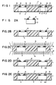
- core sheet 1 of thermoplastic resin is formed of polycarbonate resin (manufactured by Teijin under the trademark "panlite") having a thickness of, for example, 0.32 mm.
- core sheet 1 has two openings 2.
- IC chip 3 comprises a plurality of input or output electrodes 4.
- Conductive projection 5 is formed on each electrode 4.
- Conductive projection 5 is made flush with the main surface of core sheet 1.
- a conductive layer pattern 6 is formed on the main surface of core sheet 1.
- Conductive layer pattern 6 extends through part of the surface of IC chip 3, and is electrically connected with the top surface of conductive projection 5.
- the side surface of the conductive projection 5 is surrounded by the same material as that of core sheet 1.
- the upper surface of core sheet 1, including conductive pattern 6, and the lower surface of core sheet 1 are coated with insulating cover sheet 7.
- Cover sheet 7 is provided with a plurality of holes (not shown). Data is taken into or out of IC chip 3 through the holes and the conductive layer pattern 6.
- the electrode 4 deposited on IC chip 3 and the conductive layer pattern 6 are connected together without the aid of a bonding wire, thereby enabling the IC card to be fabricated with a small thickness.
- a thermoplastic insulating resin sheet prepared from the same material, for example, as core sheet 1 is interposed between the end portions of the conductive layer pattern 6 and the surface of IC chip 3. Even if, therefore, a passivation layer falls off part of the surface of IC chip 3, electric short circuiting does not arise between IC chip 3 and conductive layer pattern 6 through the fallen portion of the passivation layer.
- thermoplastic core sheet (not shown) which has at least one penetrating hole 2 and is made thicker than an IC chip.
- conductive projections 5 are mounted on electrodes 4 of IC chip 3.
- Conductive projection 5 should be made of such material as has a lesser hardness than silicon constituting IC chip 3 in order to prevent IC chip 3 from being broken when conductive projection 5 undergoes pressure.
- conductive projection 5 be prepared from a transition metal selected from the group consisting of Au, Cu, Ag, Al, Zn, Pd, Sn, Os, Pt and Ir or an low-temperature melting alloy composed of at least two metals selected from the group consisting of Pd, Sn, In, Ag, Ga, Au, Bi, Te, Ge and Sb.
- conductive projection 5 is formed of a transition metal, it is preferred to select any of the following processes: ball bonding, electroplating, vacuum deposition, sputtering, ion plating, laser growing and transcripting processes.
- a low-temperature melting alloy it is preferred to apply ultrasonic waves to the fusion of a low-temperature melting alloy and dip an IC chip in the fusion.
- conductive projection 5 may also be prepared from a mass composed of metal and resin. In this case, it is advised to mix epoxy resin with silver powder, knead them into a paste and deposit the mass on the electrode of IC chip 3.
- the height of conductive projection 5, namely a height from the surface of IC chip 3 to the surface of conductive projection 5 is preferred to be a measurement arrived at by subtracting the thickness of IC chip 3 (in this example, 0.29 mm) from the thickness of core sheet 1 (in this example, 0.32 mm), namely, larger than 30 microns.
- ball bonding involving Au was applied to the surface of the electrode of IC chip 3. Later, the bonding wire portion was cut off, thereby retaining Au balls alone on the electrode as conductive projections. In this case the height of the Au ball, namely, conductive projection 5, measured 50 microns.
- Core sheet 1 may be prepared not only from the aforementioned polycarbonate resin, but also from any of the following resins: polyvinyl chloride, polyvinyl chloride-acetate copolymer, polysulfone, polyethylene terephthalate, polyetherketone, polymethyl-pentene, polyallylate, polyether-sulfone, polyether-imide, polyphenylen-sulfide and ABS.
- core sheet 1 is sandwiched between two heating and pressurizing members each containing heating coil 8 to be heated and pressurized.
- polycarbonate core sheet 1 is heated to 200°C, and a pressure of 20 kgf/cm2 is applied between the top and bottom surfaces of core sheet 1.
- core sheet 1 undergoes plastic deformation, and a space between the side surfaces of IC chip 3 and the inner surfaces of penetrating hole 2 is filled with polycarbonate resin.
- the top surface of conductive projection 5 is made flush with the main surface of core sheet 1.
- the side surface of conductive projection 5 is covered with the material of core sheet 1, and the top surface of conductive projection 5 is exposed.
- the foregoing step may be replaced by the process of pressurizing conductive projections 5 in advance to reduce its height to a level reached by subtracting the thickness of semiconductor chip 3 from that of core sheet and thereafter pressurizing core sheet 1.
- Conductive layer pattern 6 is formed on the main surface of core sheet 1 in such a manner that an end portion of the conductive layer pattern contacts the exposed top surface of conductive projection 5.
- Conductive layer pattern 6 can be prepared by the process of mixing resin with powder of a single metal selected from the group consisting of Au, Ag, Cu, Pt, Ni, Sn, W, Mo Pd, SiC, C and RuO2, or powder of an alloy composed of at least two metals selected from the group, or powder of metal oxide to provide a conductive paste, and printing the paste.
- the content of the metal powder mixed with the resin varies with the kind of the metal.
- the powder of Ag at least 70% by weight will provide paste of high conductivity.
- conductive layer pattern 6 is formed by mixing 90% by weight of Ag powder with polycarbonate resin and screen printing the resultant Ag paste. When powder of any other metal is applied, it will serve the purpose if the resin is mixed with a sufficient amount of metal powder to render the resultant paste effectively conductive.
- a conductive layer pattern 6 can also be prepared by the process of depositing a layer of any metal selected from the group consisting of Au, Ag, Cu, Pt, Ni, Sn, W, Mo, and Pd on the surface of core sheet 1 by the process of vacuum deposition, sputtering or electroless plating and fabricating a prescribed pattern of conductive layer by photolithography.
- cover sheet 7 prepared from the same material as that of core sheet 1, is deposited on both top and bottom surfaces of core sheet 1. Cover sheet 7 is fused with the core sheet 1 and conductive layer pattern 6 by applying heat and pressure. Later, the fused mass is punched in the prescribed pattern to provide a required IC card.
- the above-mentioned IC card manufacturing method embodying the present invention offers the advantages that the IC card can be fabricated with a sufficiently small thickness; electrodes on the IC chip can obviously be connected with the conductive layer pattern without the occurrence of electric short circuiting between the surface of IC chip and the conductive layer pattern; and the IC card embodying the present invention has been experimentally proved to ensure satisfactory operating properties and high reliability.
Description
- This invention relates to an IC card and the method of manufacturing the same.
- In the Japanese Patent Application 59-196,206 the present inventors proposed a method of manufacturing an IC card which comprises the steps of embedding a semi-conductor IC chip in an insulating core sheet, forming a conductive layer pattern on the main surface of the core sheet, and electrically connecting an electrode deposited on the IC chip to the conductive layer pattern. The proposed IC card-manufacturing method offered the advantage that since the exposed electrode of an IC chip embedded in a core sheet could be directly connected to the conductive layer pattern formed on the main surface of the core sheet, it became possible to provide a thin IC card. In contrast, the conventional IC card-manufacturing method had the drawback in that when the electrode deposited on the IC chip and the conductive layer pattern were connected together by a bonding wire, the so-called loop height (a portion inevitably raised in height due to the bonding wire connection) caused the thickness of the IC card to be increased.
- In addition, the previously proposed IC card was further accompanied by the following drawback. Since the surface of the IC chip on which an electrode is formed is made flush with the main surface of the core sheet, part of the conductive layer pattern connected to the electrode contacts part of the surface of the IC chip. The surface of the IC chip is coated with a passivation layer prepared from phosphor silicate glass. Unless, therefore, the passivation layer partly falls off, the above-mentioned contact presents no difficulties. If, however, the passivation layer falls off at the above-mentioned portion, this can cause an electric short circuit between the conductive layer pattern and the IC chip.
- EP-A-0071311 discloses an IC card having a core sheet formed of an insulating material and with a recess. A semiconductor IC chip is received by the recess and rests against the base of that recess. The IC chip has an electrode with a conductive projection formed on the electrode. A conductive layer pattern is deposited on the core sheet and is connected to the conductive projection on said electrode.
- An object of this invention is to provide an IC card wherein a conductive layer pattern formed on a core sheet is extended through part of the surface of a semiconductor IC chip embedded in the core sheet, and the conductive layer pattern can be connected to the electrode formed on the IC chip without causing an electric short-circuit between the IC chip and the extended end portion of the conductive layer pattern.
- According to one aspect of this invention, there is provided an IC card comprising an insulating core sheet formed of an insulating material and having a main surface and a bottom surface, said IC card including at least one semiconductor IC chip having a main surface and a bottom surface, and at least one electrode, at least one conductive projection being formed on said electrode and having top and side surfaces, and at least one conductive layer pattern deposited on said core sheet and connected to the conductive projection on said electrode; characterized in that said core sheet has at least one through-hole in which said IC chip is received; in that said semiconductor IC chip is thinner than said core sheet and is embedded in said core sheet by the insulating material so that the top surface of said conductive projection and the bottom surface of said IC chip are flush with the main surface and bottom surface of the core sheet, respectively; in that said conductive layer pattern is deposited on the main surface of said core sheet; in that the side surface of said conductive projection and the peripheral portion of the main surface of said IC chip are covered with the material of said core sheet; and in that said conductive layer pattern is connected to said conductive projection at said top surface.
- According to another aspect of this invention, there is provided a method for manufacturing an IC card involving a thermoplastic resin core sheet and a semiconductor IC chip embedded in said core sheet, characterized in that said method comprises the steps of: preparing said thermoplastic resin core sheet with a greater thickness than that of said semiconductor IC chip and forming at least one hole penetrating said core sheet; forming a conductive projection on an electrode deposited on said semiconductor IC chip; inserting said semiconductor IC chip into said penetrating hole with said conductive projection positioned on a main surface side of said core sheet; plastically deforming said core sheet involving said inserted semiconductor IC chip by applying heat and pressure between said main and opposite surfaces, until the exposed top surface of said conductive projection is made flush with said main surface; and depositing a conductive layer pattern on said main surface so as to be contacted with said exposed top surface.
- This invention can be more fully understood from the following detailed description when taken in conjunction with the accompanying drawings, in which:
- Fig. 1 is a sectional view showing the main parts of an IC card embodying the present invention; and
- Figs. 2A to 2E are sectional views indicating the sequential steps of manufacturing the IC card representing the present invention.
- Referring to Fig. 1, core sheet 1 of thermoplastic resin is formed of polycarbonate resin (manufactured by Teijin under the trademark "panlite") having a thickness of, for example, 0.32 mm. In the example of Fig. 1 core sheet 1 has two
openings 2.Semiconductor IC chip 3, thinner than core sheet 1 (having a thickness of, for example, 0.29 mm), is embedded in eachopening 2, as illustrated in Fig. 1.IC chip 3 comprises a plurality of input oroutput electrodes 4.Conductive projection 5 is formed on eachelectrode 4.Conductive projection 5 is made flush with the main surface of core sheet 1. Aconductive layer pattern 6 is formed on the main surface of core sheet 1.Conductive layer pattern 6 extends through part of the surface ofIC chip 3, and is electrically connected with the top surface ofconductive projection 5. The side surface of theconductive projection 5 is surrounded by the same material as that of core sheet 1. The upper surface of core sheet 1, includingconductive pattern 6, and the lower surface of core sheet 1 are coated withinsulating cover sheet 7.Cover sheet 7 is provided with a plurality of holes (not shown). Data is taken into or out ofIC chip 3 through the holes and theconductive layer pattern 6. - According to the arrangement of Fig. 1, the
electrode 4 deposited onIC chip 3 and theconductive layer pattern 6 are connected together without the aid of a bonding wire, thereby enabling the IC card to be fabricated with a small thickness. Further, a thermoplastic insulating resin sheet prepared from the same material, for example, as core sheet 1, is interposed between the end portions of theconductive layer pattern 6 and the surface ofIC chip 3. Even if, therefore, a passivation layer falls off part of the surface ofIC chip 3, electric short circuiting does not arise betweenIC chip 3 andconductive layer pattern 6 through the fallen portion of the passivation layer. - Description may now be made with reference to Figs. 2A to 2E of the steps of manufacturing an IC card according to the method of the present invention. First, a thermoplastic core sheet (not shown) is provided which has at least one penetrating
hole 2 and is made thicker than an IC chip. Then, as shown in Fig. 2A,conductive projections 5 are mounted onelectrodes 4 ofIC chip 3.Conductive projection 5 should be made of such material as has a lesser hardness than silicon constitutingIC chip 3 in order to preventIC chip 3 from being broken whenconductive projection 5 undergoes pressure. - It is preferred that
conductive projection 5 be prepared from a transition metal selected from the group consisting of Au, Cu, Ag, Aℓ, Zn, Pd, Sn, Os, Pt and Ir or an low-temperature melting alloy composed of at least two metals selected from the group consisting of Pd, Sn, In, Ag, Ga, Au, Bi, Te, Ge and Sb. - Description may now be made of forming
conductive projection 5. Whenconductive projection 5 is formed of a transition metal, it is preferred to select any of the following processes: ball bonding, electroplating, vacuum deposition, sputtering, ion plating, laser growing and transcripting processes. When a low-temperature melting alloy is chosen, it is preferred to apply ultrasonic waves to the fusion of a low-temperature melting alloy and dip an IC chip in the fusion. Further,conductive projection 5 may also be prepared from a mass composed of metal and resin. In this case, it is advised to mix epoxy resin with silver powder, knead them into a paste and deposit the mass on the electrode ofIC chip 3. - The height of
conductive projection 5, namely a height from the surface ofIC chip 3 to the surface ofconductive projection 5 is preferred to be a measurement arrived at by subtracting the thickness of IC chip 3 (in this example, 0.29 mm) from the thickness of core sheet 1 (in this example, 0.32 mm), namely, larger than 30 microns. In the aforementioned example, ball bonding involving Au was applied to the surface of the electrode ofIC chip 3. Later, the bonding wire portion was cut off, thereby retaining Au balls alone on the electrode as conductive projections. In this case the height of the Au ball, namely,conductive projection 5, measured 50 microns. - Then, as shown in Fig. 2B,
IC chip 3 provided withconductive projections 5 is inserted into penetratinghole 2 having a larger opening than the outer measurement ofIC chip 3. In this case, care is taken to insertIC chip 3 in such a manner thatconductive projections 5 are set on the main surface of core sheet 1. Core sheet 1 may be prepared not only from the aforementioned polycarbonate resin, but also from any of the following resins: polyvinyl chloride, polyvinyl chloride-acetate copolymer, polysulfone, polyethylene terephthalate, polyetherketone, polymethyl-pentene, polyallylate, polyether-sulfone, polyether-imide, polyphenylen-sulfide and ABS. WhenIC chip 3 is inserted into penetratinghole 2, the rear surface ofIC chip 3 is made flush with the rear surface of core sheet 1. At this time the top ofconductive projection 5 projects 0.02 mm from the front surface (main surface) of core sheet 1. - In the next step, as shown in Fig. 2C, core sheet 1 is sandwiched between two heating and pressurizing members each containing
heating coil 8 to be heated and pressurized. Now let it be supposed that polycarbonate core sheet 1 is heated to 200°C, and a pressure of 20 kgf/cm² is applied between the top and bottom surfaces of core sheet 1. Then core sheet 1 undergoes plastic deformation, and a space between the side surfaces ofIC chip 3 and the inner surfaces of penetratinghole 2 is filled with polycarbonate resin. As a result, the top surface ofconductive projection 5 is made flush with the main surface of core sheet 1. At this time, the side surface ofconductive projection 5 is covered with the material of core sheet 1, and the top surface ofconductive projection 5 is exposed. The foregoing step may be replaced by the process of pressurizingconductive projections 5 in advance to reduce its height to a level reached by subtracting the thickness ofsemiconductor chip 3 from that of core sheet and thereafter pressurizing core sheet 1. - Later, as shown in Fig. 2D, a
conductive layer pattern 6 is formed on the main surface of core sheet 1 in such a manner that an end portion of the conductive layer pattern contacts the exposed top surface ofconductive projection 5.Conductive layer pattern 6 can be prepared by the process of mixing resin with powder of a single metal selected from the group consisting of Au, Ag, Cu, Pt, Ni, Sn, W, Mo Pd, SiC, C and RuO₂, or powder of an alloy composed of at least two metals selected from the group, or powder of metal oxide to provide a conductive paste, and printing the paste. - The content of the metal powder mixed with the resin varies with the kind of the metal. In the case of the powder of Ag, at least 70% by weight will provide paste of high conductivity. In the example of the present invention,
conductive layer pattern 6 is formed by mixing 90% by weight of Ag powder with polycarbonate resin and screen printing the resultant Ag paste. When powder of any other metal is applied, it will serve the purpose if the resin is mixed with a sufficient amount of metal powder to render the resultant paste effectively conductive. - A
conductive layer pattern 6 can also be prepared by the process of depositing a layer of any metal selected from the group consisting of Au, Ag, Cu, Pt, Ni, Sn, W, Mo, and Pd on the surface of core sheet 1 by the process of vacuum deposition, sputtering or electroless plating and fabricating a prescribed pattern of conductive layer by photolithography. - Later, as indicated in Fig. 2E,
cover sheet 7, prepared from the same material as that of core sheet 1, is deposited on both top and bottom surfaces of core sheet 1. Coversheet 7 is fused with the core sheet 1 andconductive layer pattern 6 by applying heat and pressure. Later, the fused mass is punched in the prescribed pattern to provide a required IC card. - The above-mentioned IC card manufacturing method embodying the present invention offers the advantages that the IC card can be fabricated with a sufficiently small thickness; electrodes on the IC chip can obviously be connected with the conductive layer pattern without the occurrence of electric short circuiting between the surface of IC chip and the conductive layer pattern; and the IC card embodying the present invention has been experimentally proved to ensure satisfactory operating properties and high reliability.
Claims (10)
- An IC card comprising an insulating core sheet (1) formed of an insulating material and having a main surface and a bottom surface, said IC card including at least one semiconductor IC chip (3) having a main surface and a bottom surface, and at least one electrode (4), at least one conductive projection (5) being formed on said electrode (4) and having top and side surfaces, and at least one conductive layer pattern (6) deposited on said core sheet (1) and connected to the conductive projection on said electrode (4); characterized in that said core sheet (1) has at least one through-hole (2) in which said IC chip is received; in that said semiconductor IC chip (3) is thinner than said core sheet (1) and is embedded in said core sheet (1) by the insulating material so that the top surface of said conductive projection (5) and the bottom surface of said IC chip (3) are flush with the main surface and bottom surface of the core sheet (1), respectively; in that said conductive layer pattern (6) is deposited on the main surface of said core sheet (1); in that the side surface of said conductive projection (5) and the peripheral portion of the main surface of said IC chip (3) are covered with the material of said core sheet (3); and in that said conductive layer pattern (6) is connected to said conductive projection (5) at said top surface.
- An IC card according to claim 1, characterized in that said conductive projection (5) is prepared from a softer material than said semiconductor IC chip.
- An IC card according to claim 2, characterized in that said conductive projection (5) is prepared from at least one metal selected from the group consisting of Au, Cu, Ag, Aℓ, Zn, Pd, Sn, Os, Pt and Ir.
- An IC card according to claim 2, characterized in that said conductive projection (5) is made of an alloy prepared from at least two metals selected from the group consisting of Pd, Sn, In, Ag, Ga, Au, Bi, Te, Ge and Sb.
- An IC card according to claim 2, characterized in that said conductive projection (5) is prepared from a mass composed of a metal and a resin.
- An IC card according to claim 1, characterized in that said thermoplastic core sheet (1) is prpepared from at least one resin selected from the group consisting of polycarbonate, polyvinyl chloride, polyvinyl chloride-acetate copolymer, polysulfone, polyethylene terephthalate, polyetherketone, polymethylpenten, polyallylate, polyether-sulfone, polyether-imide, polyphenylene-sulfide and ABS.
- A method for manufacturing an IC card involving a thermoplastic resin core sheet and a semiconductor IC chip embedded in said core sheet, characterized in that said method comprises the steps of: preparing said thermoplastic resin core sheet (1) with a greater thickness than that of said semiconductor IC chip (3) and forming at least one hole (2) penetrating said core sheet (1); forming a conductive projection (5) on an electrode (4) deposited on said semiconductor IC chip (3); inserting said semiconductor IC chip into said penetrating hole with said conductive projection (5) positioned on a main surface side of said core sheet; plastically deforming said core sheet (1) involving said inserted semiconductor IC chip by applying heat and pressure between said main and opposite surfaces, until the exposed top surface of said conductive projection is made flush with said main surface; and depositing a conductive layer pattern (6) on said main surface so as to be contacted with said exposed top surface.
- An IC card-manufacturing method according to claim 7, characterized in that said conductive projection (5) is formed by any of the following processes: ball bonding, electroplating, vacuum deposition, sputtering, ion plating, laser growing, transcripting, dipping and dispensing.
- An IC card-manufacturing method according to claim 7, characterized in that said conductive layer pattern (6) is printed on the surface of the thermoplastic resin core sheet (1) by means of conductive paste formed by kneading at least one of the groups consisting of metal powder, metal alloy powder and metal oxide powder with a resin, said metal powder being prepared from at least one metal selected from the group consisting of Au, Ag, Cu, Pt, Ni, Sn, W, Mo, Pd, SiC, C and RuO₂ and said metal alloy powder being formed of a metal alloy composed of at least two of said metal group.
- An IC card-manufacturing method according to claim 8, characterized in that said conductive layer pattern (6) is prepared by depositing at least one metal selected from the group consisting of Au, Ag, Cu, Pt, Ni, Sn, W and Mo on the main surface of said core sheet by one of the following processes: vacuum depositing, sputtering, electroless plating, and then patterning said deposited metal layer by means of photolithography.
Applications Claiming Priority (2)
| Application Number | Priority Date | Filing Date | Title |
|---|---|---|---|
| JP115585/86 | 1986-05-20 | ||
| JP61115585A JPH074995B2 (en) | 1986-05-20 | 1986-05-20 | IC card and method of manufacturing the same |
Publications (3)
| Publication Number | Publication Date |
|---|---|
| EP0246744A2 EP0246744A2 (en) | 1987-11-25 |
| EP0246744A3 EP0246744A3 (en) | 1989-06-14 |
| EP0246744B1 true EP0246744B1 (en) | 1992-12-09 |
Family
ID=14666233
Family Applications (1)
| Application Number | Title | Priority Date | Filing Date |
|---|---|---|---|
| EP87302805A Expired - Lifetime EP0246744B1 (en) | 1986-05-20 | 1987-03-31 | Ic card and method of manufacturing the same |
Country Status (5)
| Country | Link |
|---|---|
| US (2) | US4931853A (en) |
| EP (1) | EP0246744B1 (en) |
| JP (1) | JPH074995B2 (en) |
| KR (1) | KR900003803B1 (en) |
| DE (1) | DE3782972T2 (en) |
Families Citing this family (78)
| Publication number | Priority date | Publication date | Assignee | Title |
|---|---|---|---|---|
| FR2625067A1 (en) * | 1987-12-22 | 1989-06-23 | Sgs Thomson Microelectronics | METHOD FOR ATTACHING AN ELECTRONIC COMPONENT AND CONTACTS TO IT |
| JPH03500033A (en) * | 1988-06-21 | 1991-01-10 | ダブリュー アンド ティー エイヴァリー リミテッド | How to make portable electronic tokens |
| BE1002529A6 (en) * | 1988-09-27 | 1991-03-12 | Bell Telephone Mfg | Method for an electronic component assembly and memory card in which it is applied. |
| USRE35578E (en) * | 1988-12-12 | 1997-08-12 | Sgs-Thomson Microelectronics, Inc. | Method to install an electronic component and its electrical connections on a support, and product obtained thereby |
| US5182420A (en) * | 1989-04-25 | 1993-01-26 | Cray Research, Inc. | Method of fabricating metallized chip carriers from wafer-shaped substrates |
| US5412247A (en) * | 1989-07-28 | 1995-05-02 | The Charles Stark Draper Laboratory, Inc. | Protection and packaging system for semiconductor devices |
| US5155068A (en) * | 1989-08-31 | 1992-10-13 | Sharp Kabushiki Kaisha | Method for manufacturing an IC module for an IC card whereby an IC device and surrounding encapsulant are thinned by material removal |
| US5081563A (en) * | 1990-04-27 | 1992-01-14 | International Business Machines Corporation | Multi-layer package incorporating a recessed cavity for a semiconductor chip |
| US5227338A (en) * | 1990-04-30 | 1993-07-13 | International Business Machines Corporation | Three-dimensional memory card structure with internal direct chip attachment |
| JPH0429338A (en) * | 1990-05-24 | 1992-01-31 | Nippon Mektron Ltd | Method circuit board for mounting ic and its mounting |
| US5241456A (en) * | 1990-07-02 | 1993-08-31 | General Electric Company | Compact high density interconnect structure |
| JP2560895B2 (en) * | 1990-07-25 | 1996-12-04 | 三菱電機株式会社 | IC card manufacturing method and IC card |
| US5196377A (en) * | 1990-12-20 | 1993-03-23 | Cray Research, Inc. | Method of fabricating silicon-based carriers |
| FR2672427A1 (en) * | 1991-02-04 | 1992-08-07 | Schiltz Andre | METHOD AND DEVICE FOR INSERTING CHIPS INTO HOUSINGS OF A SUBSTRATE BY INTERMEDIATE FILM. |
| JP2816028B2 (en) * | 1991-02-18 | 1998-10-27 | 株式会社東芝 | Method for manufacturing semiconductor device |
| JPH06122297A (en) * | 1992-08-31 | 1994-05-06 | Sony Chem Corp | Ic card and manufacture thereof |
| DE69325065T2 (en) * | 1992-10-02 | 1999-10-28 | Matsushita Electric Ind Co Ltd | Semiconductor device, image scanner and method of manufacturing the same |
| KR0137398B1 (en) * | 1992-10-23 | 1998-04-29 | 모리시타 요이찌 | Fabrication method of sensor & unit |
| ZA941671B (en) * | 1993-03-11 | 1994-10-12 | Csir | Attaching an electronic circuit to a substrate. |
| US5422514A (en) * | 1993-05-11 | 1995-06-06 | Micromodule Systems, Inc. | Packaging and interconnect system for integrated circuits |
| US5689136A (en) * | 1993-08-04 | 1997-11-18 | Hitachi, Ltd. | Semiconductor device and fabrication method |
| JP3348528B2 (en) * | 1994-07-20 | 2002-11-20 | 富士通株式会社 | Method for manufacturing semiconductor device, method for manufacturing semiconductor device and electronic circuit device, and electronic circuit device |
| ATE167319T1 (en) * | 1994-11-03 | 1998-06-15 | Fela Holding Ag | BASE FILM FOR CHIP CARD |
| US5952713A (en) * | 1994-12-27 | 1999-09-14 | Takahira; Kenichi | Non-contact type IC card |
| FR2735284B1 (en) * | 1995-06-12 | 1997-08-29 | Solaic Sa | CHIP FOR ELECTRONIC CARD COATED WITH A LAYER OF INSULATING MATERIAL AND ELECTRONIC CARD CONTAINING SUCH A CHIP |
| US5874780A (en) * | 1995-07-27 | 1999-02-23 | Nec Corporation | Method of mounting a semiconductor device to a substrate and a mounted structure |
| DE19528730A1 (en) * | 1995-08-04 | 1997-02-06 | Giesecke & Devrient Gmbh | Process for the production of a data carrier |
| US6441736B1 (en) | 1999-07-01 | 2002-08-27 | Keith R. Leighton | Ultra-thin flexible durable radio frequency identification devices and hot or cold lamination process for the manufacture of ultra-thin flexible durable radio frequency identification devices |
| US5817207A (en) | 1995-10-17 | 1998-10-06 | Leighton; Keith R. | Radio frequency identification card and hot lamination process for the manufacture of radio frequency identification cards |
| US6036099A (en) | 1995-10-17 | 2000-03-14 | Leighton; Keith | Hot lamination process for the manufacture of a combination contact/contactless smart card and product resulting therefrom |
| US5674785A (en) * | 1995-11-27 | 1997-10-07 | Micron Technology, Inc. | Method of producing a single piece package for semiconductor die |
| US6013948A (en) * | 1995-11-27 | 2000-01-11 | Micron Technology, Inc. | Stackable chip scale semiconductor package with mating contacts on opposed surfaces |
| US6861290B1 (en) * | 1995-12-19 | 2005-03-01 | Micron Technology, Inc. | Flip-chip adaptor package for bare die |
| US5811879A (en) * | 1996-06-26 | 1998-09-22 | Micron Technology, Inc. | Stacked leads-over-chip multi-chip module |
| WO1998052772A1 (en) * | 1997-05-19 | 1998-11-26 | Hitachi Maxell, Ltd. | Flexible ic module and method of its manufacture, and method of manufacturing information carrier comprising flexible ic module |
| US5899705A (en) * | 1997-11-20 | 1999-05-04 | Akram; Salman | Stacked leads-over chip multi-chip module |
| EP0942392A3 (en) * | 1998-03-13 | 2000-10-18 | Kabushiki Kaisha Toshiba | Chip card |
| US6241153B1 (en) * | 1998-03-17 | 2001-06-05 | Cardxx, Inc. | Method for making tamper-preventing, contact-type, smart cards |
| USRE43112E1 (en) | 1998-05-04 | 2012-01-17 | Round Rock Research, Llc | Stackable ball grid array package |
| US6040622A (en) * | 1998-06-11 | 2000-03-21 | Sandisk Corporation | Semiconductor package using terminals formed on a conductive layer of a circuit board |
| US6414391B1 (en) | 1998-06-30 | 2002-07-02 | Micron Technology, Inc. | Module assembly for stacked BGA packages with a common bus bar in the assembly |
| TW368707B (en) * | 1998-10-27 | 1999-09-01 | Tech Field Co Ltd | Packaging method for semiconductor die and the product of the same |
| FR2790849B1 (en) | 1999-03-12 | 2001-04-27 | Gemplus Card Int | MANUFACTURING METHOD FOR CONTACTLESS CARD TYPE ELECTRONIC DEVICE |
| JP3517374B2 (en) * | 1999-05-21 | 2004-04-12 | 新光電気工業株式会社 | Method for manufacturing non-contact type IC card |
| FR2794266B1 (en) * | 1999-05-25 | 2002-01-25 | Gemplus Card Int | METHOD FOR MANUFACTURING PORTABLE ELECTRONIC DEVICE WITH INTEGRATED CIRCUIT HAVING LOW COST DIELECTRIC |
| FR2794265B1 (en) | 1999-05-25 | 2003-09-19 | Gemplus Card Int | METHOD FOR MANUFACTURING SMART CONTACT CARDS WITH LOW COST DIELECTRICS |
| WO2001005602A1 (en) * | 1999-07-21 | 2001-01-25 | Ibiden Co., Ltd. | Pc card and method for manufacturing the same |
| JP3864029B2 (en) * | 2000-03-24 | 2006-12-27 | 松下電器産業株式会社 | Semiconductor package and semiconductor package manufacturing method |
| DE10016715C1 (en) * | 2000-04-04 | 2001-09-06 | Infineon Technologies Ag | Laminated smart card arrangement e.g. for telephone card |
| JP4403631B2 (en) * | 2000-04-24 | 2010-01-27 | ソニー株式会社 | Manufacturing method of chip-shaped electronic component and manufacturing method of pseudo wafer used for manufacturing the same |
| JP2001313350A (en) * | 2000-04-28 | 2001-11-09 | Sony Corp | Chip-shaped electronic component and its manufacturing method, and pseudo-wafer used for manufacture of chip- shaped electronic component and its manufacturing method |
| US20020175402A1 (en) * | 2001-05-23 | 2002-11-28 | Mccormack Mark Thomas | Structure and method of embedding components in multi-layer substrates |
| US6545227B2 (en) | 2001-07-11 | 2003-04-08 | Mce/Kdi Corporation | Pocket mounted chip having microstrip line |
| US6506632B1 (en) * | 2002-02-15 | 2003-01-14 | Unimicron Technology Corp. | Method of forming IC package having downward-facing chip cavity |
| JP3678212B2 (en) * | 2002-05-20 | 2005-08-03 | ウシオ電機株式会社 | Super high pressure mercury lamp |
| US6972964B2 (en) * | 2002-06-27 | 2005-12-06 | Via Technologies Inc. | Module board having embedded chips and components and method of forming the same |
| TW546800B (en) * | 2002-06-27 | 2003-08-11 | Via Tech Inc | Integrated moduled board embedded with IC chip and passive device and its manufacturing method |
| US6755700B2 (en) * | 2002-11-12 | 2004-06-29 | Modevation Enterprises Inc. | Reset speed control for watercraft |
| US7312101B2 (en) * | 2003-04-22 | 2007-12-25 | Micron Technology, Inc. | Packaged microelectronic devices and methods for packaging microelectronic devices |
| US7408258B2 (en) * | 2003-08-20 | 2008-08-05 | Salmon Technologies, Llc | Interconnection circuit and electronic module utilizing same |
| US20050184376A1 (en) * | 2004-02-19 | 2005-08-25 | Salmon Peter C. | System in package |
| US7427809B2 (en) * | 2004-12-16 | 2008-09-23 | Salmon Technologies, Llc | Repairable three-dimensional semiconductor subsystem |
| US20070007983A1 (en) * | 2005-01-06 | 2007-01-11 | Salmon Peter C | Semiconductor wafer tester |
| CA2601512A1 (en) | 2005-03-23 | 2006-09-28 | Cardxx, Inc. | Method for making advanced smart cards with integrated electronics using isotropic thermoset adhesive materials with high quality exterior surfaces |
| JP4657840B2 (en) * | 2005-07-14 | 2011-03-23 | 新藤電子工業株式会社 | Semiconductor device and manufacturing method thereof |
| US20070023904A1 (en) * | 2005-08-01 | 2007-02-01 | Salmon Peter C | Electro-optic interconnection apparatus and method |
| US7586747B2 (en) * | 2005-08-01 | 2009-09-08 | Salmon Technologies, Llc. | Scalable subsystem architecture having integrated cooling channels |
| US20070023889A1 (en) * | 2005-08-01 | 2007-02-01 | Salmon Peter C | Copper substrate with feedthroughs and interconnection circuits |
| US20070023923A1 (en) * | 2005-08-01 | 2007-02-01 | Salmon Peter C | Flip chip interface including a mixed array of heat bumps and signal bumps |
| JP5164362B2 (en) * | 2005-11-02 | 2013-03-21 | キヤノン株式会社 | Semiconductor embedded substrate and manufacturing method thereof |
| TWI325745B (en) | 2006-11-13 | 2010-06-01 | Unimicron Technology Corp | Circuit board structure and fabrication method thereof |
| TW200836315A (en) * | 2007-02-16 | 2008-09-01 | Richtek Techohnology Corp | Electronic package structure and method thereof |
| US7557489B2 (en) * | 2007-07-10 | 2009-07-07 | Siemens Medical Solutions Usa, Inc. | Embedded circuits on an ultrasound transducer and method of manufacture |
| US7514290B1 (en) * | 2008-04-24 | 2009-04-07 | International Business Machines Corporation | Chip-to-wafer integration technology for three-dimensional chip stacking |
| TW201136468A (en) * | 2010-04-06 | 2011-10-16 | Chung-Cheng Wang | A printing circuit board and being used |
| WO2014006787A1 (en) * | 2012-07-04 | 2014-01-09 | パナソニック株式会社 | Electronic component mounting structure, ic card, and cof package |
| US9627338B2 (en) * | 2013-03-06 | 2017-04-18 | STATS ChipPAC Pte. Ltd. | Semiconductor device and method of forming ultra high density embedded semiconductor die package |
| US10181449B1 (en) * | 2017-09-28 | 2019-01-15 | Taiwan Semiconductor Manufacturing Co., Ltd. | Semiconductor structure |
Family Cites Families (11)
| Publication number | Priority date | Publication date | Assignee | Title |
|---|---|---|---|---|
| DE2102421C3 (en) * | 1971-01-19 | 1979-09-06 | Siemens Ag, 1000 Berlin Und 8000 Muenchen | Process for the production of a structured metallic layer on a ceramic base body |
| JPS5230184A (en) * | 1975-09-02 | 1977-03-07 | Sharp Corp | Semiconductor device |
| US4214904A (en) * | 1978-12-12 | 1980-07-29 | The United States Of America As Represented By The Secretary Of The Air Force | Gold-tin-silicon alloy for brazing silicon to metal |
| JPS577142A (en) * | 1980-06-16 | 1982-01-14 | Toshiba Corp | Marking method of resin-sealed semiconductor device |
| JPS577147A (en) * | 1980-06-17 | 1982-01-14 | Citizen Watch Co Ltd | Mounting construction of semiconductor device |
| FR2489043A1 (en) * | 1980-08-20 | 1982-02-26 | Thomson Csf | Attaching semiconductor wafer to housing base plate - brazing or soldering using screen printed paste of braze metal or solder |
| FR2492164B1 (en) * | 1980-10-15 | 1987-01-23 | Radiotechnique Compelec | METHOD FOR THE SIMULTANEOUS REALIZATION OF MULTIPLE ELECTRICAL LINKS, PARTICULARLY FOR THE ELECTRICAL CONNECTION OF A SEMICONDUCTOR MICRO-WAFER |
| DE8122540U1 (en) * | 1981-07-31 | 1983-01-13 | Philips Patentverwaltung Gmbh, 2000 Hamburg | "INFORMATION CARD WITH INTEGRATED BLOCK" |
| JPS58173790A (en) * | 1982-04-06 | 1983-10-12 | シチズン時計株式会社 | Connection structure of display unit and semiconductor device |
| FR2527036A1 (en) * | 1982-05-14 | 1983-11-18 | Radiotechnique Compelec | METHOD FOR CONNECTING A SEMICONDUCTOR TO ELEMENTS OF A SUPPORT, PARTICULARLY A PORTABLE CARD |
| JPS6175488A (en) * | 1984-09-19 | 1986-04-17 | Toshiba Corp | Manufacture of ic card |
-
1986
- 1986-05-20 JP JP61115585A patent/JPH074995B2/en not_active Expired - Fee Related
-
1987
- 1987-03-31 DE DE8787302805T patent/DE3782972T2/en not_active Expired - Fee Related
- 1987-03-31 EP EP87302805A patent/EP0246744B1/en not_active Expired - Lifetime
- 1987-05-18 KR KR1019870004878A patent/KR900003803B1/en not_active IP Right Cessation
-
1989
- 1989-09-06 US US07/403,772 patent/US4931853A/en not_active Expired - Fee Related
-
1990
- 1990-04-13 US US07/508,649 patent/US4997791A/en not_active Expired - Fee Related
Also Published As
| Publication number | Publication date |
|---|---|
| DE3782972T2 (en) | 1993-04-29 |
| KR900003803B1 (en) | 1990-05-31 |
| DE3782972D1 (en) | 1993-01-21 |
| EP0246744A2 (en) | 1987-11-25 |
| EP0246744A3 (en) | 1989-06-14 |
| JPS62270393A (en) | 1987-11-24 |
| JPH074995B2 (en) | 1995-01-25 |
| US4997791A (en) | 1991-03-05 |
| KR880014641A (en) | 1988-12-24 |
| US4931853A (en) | 1990-06-05 |
Similar Documents
| Publication | Publication Date | Title |
|---|---|---|
| EP0246744B1 (en) | Ic card and method of manufacturing the same | |
| US4442966A (en) | Method of simultaneously manufacturing multiple electrical connections between two electrical elements | |
| EP0308971B1 (en) | Bump and method of manufacturing the same | |
| US7777352B2 (en) | Semiconductor device with semiconductor device components embedded in plastic package compound | |
| US4363076A (en) | Integrated circuit package | |
| US4437235A (en) | Integrated circuit package | |
| EP2224479B1 (en) | Metal-ceramic composite substrate and method of its manufacture | |
| EP0706208A2 (en) | Semiconductor package integral with semiconductor chip and method of manufacturing thereof | |
| US6093964A (en) | Connection structure utilizing a metal bump and metal bump manufacturing method | |
| US6614113B2 (en) | Semiconductor device and method for producing the same | |
| CN102652358B (en) | Based on the leadframe package method and apparatus of panel | |
| KR100366173B1 (en) | Protection circuit device comprising mosfet and method of manufacturing the same | |
| US4907061A (en) | Electronic device | |
| JP3639515B2 (en) | Method for manufacturing MOSFET mounting structure | |
| US6087712A (en) | Lead frame containing leads plated with tin alloy for increased wettability and method for plating the leads | |
| CA1209653A (en) | Solid electrolyte capacitor | |
| US5760466A (en) | Semiconductor device having improved heat resistance | |
| US6529115B2 (en) | Surface mounted resistor | |
| US7746213B2 (en) | Device and method for manufacturing the same | |
| JPH071790B2 (en) | Method for manufacturing plug-in type semiconductor package | |
| JP2627509B2 (en) | Electronic component having conductive layer | |
| CN110890284A (en) | Chip stacking and packaging structure and process method thereof | |
| JP2575749B2 (en) | Method for manufacturing lead in semiconductor device | |
| EP0154187B1 (en) | Tape bonding material and structure for electronic circuit fabrication | |
| JPS6221267B2 (en) |
Legal Events
| Date | Code | Title | Description |
|---|---|---|---|
| PUAI | Public reference made under article 153(3) epc to a published international application that has entered the european phase |
Free format text: ORIGINAL CODE: 0009012 |
|
| AK | Designated contracting states |
Kind code of ref document: A2 Designated state(s): DE FR |
|
| 17P | Request for examination filed |
Effective date: 19880209 |
|
| PUAL | Search report despatched |
Free format text: ORIGINAL CODE: 0009013 |
|
| AK | Designated contracting states |
Kind code of ref document: A3 Designated state(s): DE FR |
|
| 17Q | First examination report despatched |
Effective date: 19910128 |
|
| GRAA | (expected) grant |
Free format text: ORIGINAL CODE: 0009210 |
|
| AK | Designated contracting states |
Kind code of ref document: B1 Designated state(s): DE FR |
|
| REF | Corresponds to: |
Ref document number: 3782972 Country of ref document: DE Date of ref document: 19930121 |
|
| ET | Fr: translation filed | ||
| PLBE | No opposition filed within time limit |
Free format text: ORIGINAL CODE: 0009261 |
|
| STAA | Information on the status of an ep patent application or granted ep patent |
Free format text: STATUS: NO OPPOSITION FILED WITHIN TIME LIMIT |
|
| 26N | No opposition filed | ||
| PGFP | Annual fee paid to national office [announced via postgrant information from national office to epo] |
Ref country code: DE Payment date: 19991231 Year of fee payment: 14 |
|
| PGFP | Annual fee paid to national office [announced via postgrant information from national office to epo] |
Ref country code: FR Payment date: 20000310 Year of fee payment: 14 |
|
| PG25 | Lapsed in a contracting state [announced via postgrant information from national office to epo] |
Ref country code: FR Free format text: LAPSE BECAUSE OF NON-PAYMENT OF DUE FEES Effective date: 20011130 |
|
| REG | Reference to a national code |
Ref country code: FR Ref legal event code: ST |
|
| PG25 | Lapsed in a contracting state [announced via postgrant information from national office to epo] |
Ref country code: DE Free format text: LAPSE BECAUSE OF NON-PAYMENT OF DUE FEES Effective date: 20020101 |