EP0241562A1 - Liquid crystal display device - Google Patents
Liquid crystal display device Download PDFInfo
- Publication number
- EP0241562A1 EP0241562A1 EP86906432A EP86906432A EP0241562A1 EP 0241562 A1 EP0241562 A1 EP 0241562A1 EP 86906432 A EP86906432 A EP 86906432A EP 86906432 A EP86906432 A EP 86906432A EP 0241562 A1 EP0241562 A1 EP 0241562A1
- Authority
- EP
- European Patent Office
- Prior art keywords
- polarity
- liquid
- picture
- circuit
- crystal panel
- Prior art date
- Legal status (The legal status is an assumption and is not a legal conclusion. Google has not performed a legal analysis and makes no representation as to the accuracy of the status listed.)
- Granted
Links
Images


Classifications
-
- H—ELECTRICITY
- H04—ELECTRIC COMMUNICATION TECHNIQUE
- H04N—PICTORIAL COMMUNICATION, e.g. TELEVISION
- H04N5/00—Details of television systems
- H04N5/66—Transforming electric information into light information
-
- G—PHYSICS
- G09—EDUCATION; CRYPTOGRAPHY; DISPLAY; ADVERTISING; SEALS
- G09G—ARRANGEMENTS OR CIRCUITS FOR CONTROL OF INDICATING DEVICES USING STATIC MEANS TO PRESENT VARIABLE INFORMATION
- G09G3/00—Control arrangements or circuits, of interest only in connection with visual indicators other than cathode-ray tubes
- G09G3/20—Control arrangements or circuits, of interest only in connection with visual indicators other than cathode-ray tubes for presentation of an assembly of a number of characters, e.g. a page, by composing the assembly by combination of individual elements arranged in a matrix no fixed position being assigned to or needed to be assigned to the individual characters or partial characters
- G09G3/34—Control arrangements or circuits, of interest only in connection with visual indicators other than cathode-ray tubes for presentation of an assembly of a number of characters, e.g. a page, by composing the assembly by combination of individual elements arranged in a matrix no fixed position being assigned to or needed to be assigned to the individual characters or partial characters by control of light from an independent source
- G09G3/36—Control arrangements or circuits, of interest only in connection with visual indicators other than cathode-ray tubes for presentation of an assembly of a number of characters, e.g. a page, by composing the assembly by combination of individual elements arranged in a matrix no fixed position being assigned to or needed to be assigned to the individual characters or partial characters by control of light from an independent source using liquid crystals
- G09G3/3611—Control of matrices with row and column drivers
- G09G3/3614—Control of polarity reversal in general
-
- G—PHYSICS
- G09—EDUCATION; CRYPTOGRAPHY; DISPLAY; ADVERTISING; SEALS
- G09G—ARRANGEMENTS OR CIRCUITS FOR CONTROL OF INDICATING DEVICES USING STATIC MEANS TO PRESENT VARIABLE INFORMATION
- G09G3/00—Control arrangements or circuits, of interest only in connection with visual indicators other than cathode-ray tubes
- G09G3/20—Control arrangements or circuits, of interest only in connection with visual indicators other than cathode-ray tubes for presentation of an assembly of a number of characters, e.g. a page, by composing the assembly by combination of individual elements arranged in a matrix no fixed position being assigned to or needed to be assigned to the individual characters or partial characters
- G09G3/34—Control arrangements or circuits, of interest only in connection with visual indicators other than cathode-ray tubes for presentation of an assembly of a number of characters, e.g. a page, by composing the assembly by combination of individual elements arranged in a matrix no fixed position being assigned to or needed to be assigned to the individual characters or partial characters by control of light from an independent source
- G09G3/36—Control arrangements or circuits, of interest only in connection with visual indicators other than cathode-ray tubes for presentation of an assembly of a number of characters, e.g. a page, by composing the assembly by combination of individual elements arranged in a matrix no fixed position being assigned to or needed to be assigned to the individual characters or partial characters by control of light from an independent source using liquid crystals
- G09G3/3611—Control of matrices with row and column drivers
- G09G3/3648—Control of matrices with row and column drivers using an active matrix
- G09G3/3655—Details of drivers for counter electrodes, e.g. common electrodes for pixel capacitors or supplementary storage capacitors
-
- H—ELECTRICITY
- H04—ELECTRIC COMMUNICATION TECHNIQUE
- H04N—PICTORIAL COMMUNICATION, e.g. TELEVISION
- H04N3/00—Scanning details of television systems; Combination thereof with generation of supply voltages
- H04N3/10—Scanning details of television systems; Combination thereof with generation of supply voltages by means not exclusively optical-mechanical
- H04N3/12—Scanning details of television systems; Combination thereof with generation of supply voltages by means not exclusively optical-mechanical by switched stationary formation of lamps, photocells or light relays
- H04N3/127—Scanning details of television systems; Combination thereof with generation of supply voltages by means not exclusively optical-mechanical by switched stationary formation of lamps, photocells or light relays using liquid crystals
-
- G—PHYSICS
- G09—EDUCATION; CRYPTOGRAPHY; DISPLAY; ADVERTISING; SEALS
- G09G—ARRANGEMENTS OR CIRCUITS FOR CONTROL OF INDICATING DEVICES USING STATIC MEANS TO PRESENT VARIABLE INFORMATION
- G09G2320/00—Control of display operating conditions
- G09G2320/02—Improving the quality of display appearance
- G09G2320/0247—Flicker reduction other than flicker reduction circuits used for single beam cathode-ray tubes
Definitions
- the present invention relates to a liquid-crystal display apparatus using a liquid-crystal matrix panel, and particularly to the driving circuit.
- FIG. 11 One example of the electrode circuit diagram of the active matrix panel using TFT (thin film transistor) in the liquid-crystal television is shown in Fig. 11.
- (1) ... in Fig. 11 are segment electrodes formed on the first base plate
- (2) , (2) ... are the TFT (thin film transistor) formed on the first base plate, corresponding to the respective segment electrodes (1), (1) ..., are connected with the segment electrodes (1), (1) ... corresponding to the sources of the TFT (2), (2) .... (3)
- (3) ... are drain lines connected with the drains for each of the rows of the TFT (2), (2) ... corresponding to the segment electrodes (1), (1) ... of the row direction
- (4), (4) ... are gate lines connected with the gates for each of the columns of the TFT (2), (2) corresponding to the segment electrodes (1), (1) ... of the column direction.
- (5) is a common electrode formed on the second base plate opposite to the first base plate with each of the segment electrodes (1), (1) ..., the TFT (2), (2) ..., the drain lines (3), (3) ..., the gate lines (4), (4) ... being formed thereon, the liquid crystal is filled between the first, second base plates.
- the number of the columns i.e., the number of the gate lines (4), (4) is 240, corresponds to approximately the number of the effective scanning lines among the number of the scanning lines 262.5 of one field of the NISC system.
- picture signals are applied upon the drain lines (3), (3) of the active matrix panel, and when the liquid crystal is normally driven, the AC driving is preferable, namely, the polarity of the signal is desired to be inverted at a given period through the consideration of the durability or the like when the liquid crystal is normally driven, with the picture signal becoming like, for example, Fig. 12.
- the nth of the odd-number field is On
- the nth of the even-number field is En
- the polarity is reversed for each of the fields as the odd-number fields (01), (02) become positive in polarity
- the even-number fields (E1), (E2) become negative in polarity.
- the period by which the' same element is driven by the same polarity becomes 1/30 seconds, i.e., one frame period. Accordingly, the flicker (flitting) on the picture face by the polarity reversion is hardly conspicuous.
- the number of the columns is 240 with the number of the picture elements being limited, thus providing the picture face comparatively low in the resolving degree.
- the method of improving the picture quality is proposed with the number of the picture elements being increased as 480 in the number of the columns.
- the electrode circuit diagram of the active matrix panel in the second conventional embodiment is shown in Fig. 13, the same numerals are given to the same portions as those of Fig. 11 to omit the description.
- the gate lines (41), (4'2) ... in Fig. 13 are 480, are respectively taken out to left, to right for each of the columns, the gate signals are applied upon the gate line (41) ... in the odd-number field, the gate signals are applied upon the gate line (42) ... in the even-number field.
- the flickers are caused at the one-frame period as shown in Fig. 15(b) with respect to the driving waveform of the two-frame period shown in Fig. 15(a) when the LCD panel (1) is seen from the front face, but the brilliance is reduced as shown in Fig. 15(c) in a case where 10° is deviated from, for example, the front face when the LCD panel (1) is obliquely seen, the period of the flicker becomes also the two-frame period to make the flicker more conspicuous.
- an object of the present invention is to increase the number. of the columns of the color matrix display apparatus from, for example, 240 to 480 to increase the number of the picture elements so that the flickers on the picture face through the AC driving operation of the liquid crystal is made inconspicuous.
- the present invention is adapted to reverse the polarity of the picture signals to be applied for one display picture element adjacent within at least the same column or each plural-display picture elements, the flickers of the entire picture face is visually compensated by the above-described means.
- the present invention is adapted to reverse the polarity of the picture signal for one horizontal scanning period or for each plural-horizontal scanning periods so that the brilliance of each portion on the picture face becomes uniform by the above-described means, also, to prevent the horizontal stripes.
- the present invention proposes the driving circuit of the liquid-crystal display apparatus, which is composed of a liquid-crystal panel with a plurality of display elements being arranged in columns and rows thereon, a polarity reversion circuit for reversing for each field the polarity of the picture signal to be applied upon the liquid-crystal panel, a circuit for feeding the first or second DC voltage selected for each field to the opposite electrode of said liquid-crystal panel, and a brilliance level adjusting circuit for simultaneously varying mutually in the opposite direction said first and second DC voltages to adjust the brilliance level of said picture signal, so that the brilliance level may be varied without any changes in the DC level of the picture signal through the above-described means.
- liquid-crystal display apparatus in accordance with the present invention will be described hereinafter in detail with reference to the embodiment shown in the drawings.
- Fig. 1 is a block diagram of a driving circuit of the liquid-crystal display apparatus in one embodiment of the present invention.
- Fig. 2 is a waveform chart in the essential portions of Fig. 1.
- Fig. 3 is a block diagram of the driving circuit of the liquid-crystal display apparatus in the second embodiment of the present invention.
- Fig. 4 is the waveform chart in the essential portions of Fig. 2.
- Fig. 5 is a circuit diagram of the driving circuit of the liquid-crystal display apparatus in the third embodiment of the present invention.
- Fig. 6 through Fig. 9 are respectively the circuit diagrams showing the modified embodiments of Fig. 5.
- Fig. 10 is the waveform view showing the relationship between the opposed electrode electric potential in the circuit of Fig. 5 and the picture signal.
- Fig. 10 is the waveform view showing the relationship between the opposed electrode electric potential in the circuit of Fig. 5 and the picture signal.
- Fig. 11 is an electrode circuit diagram of the active matrix panel of the conventional 240 columns.
- Fig. 12 is a picture signal waveform chart to be applied upon the panel of Fig. 11.
- rig. 13 is an electrode circuit diagram of the active matrix panel of the conventional 480 columns.
- Fig. 14 is a picture signal waveform chart to be applied upon the panel of Fig. 13.
- Figs. 15(a) and 15(b) are waveform charts for explaining the flickers.
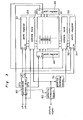
- Fig. 1 and Fig. 2 show a first embodiment of the present invention.
- Fig. 1 is a block diagram of the present embodiment circuit, which is broadly composed of an LCD panel 10, first and second row driving portions 20 and 30, first and second column driving portions 40 and 50, first and second polarity reversion circuits 60 and 70, and a synchronous control circuit 80.
- the LCD panel 10 has a mosaic-shaped color filter opposed to the active matrix panels of 480 in the number of the columns, color unit display elements are arranged like G, R, B ... sequentially in the horizontal direction for the upper left portion.
- the first and second row driving portions 20 and 30 are composed of first and second shift registers 21 and 31 to which the clock pulse (CP) and the first start pulse (ST 1 ) to be caused from the synchronous control circuit 80 are respectively fed, and first and second sample hold circuits 22 and 23 to which the output pulse of each digit of the shift register is fed as the sampling pulse sample the picture signal outputs of the first or the second polarity reversing circuits 60 and 70 and hold them for one horizontal scanning period with the horizontal synchronous pulse (HP), the picture elements in the odd-numbered rows are driven by the first sample hold circuit outputs, the picture elements in the even-numbered rows are driven by the second sample hold circuit outputs.
- first and second shift registers 21 and 31 to which the clock pulse (CP) and the first start pulse (ST 1 ) to be caused from the synchronous control circuit 80 are respectively fed
- first and second sample hold circuits 22 and 23 to which the output pulse of each digit of the shift register is fed as the sampling pulse sample the picture signal outputs of the first or the second polarity
- the first column driving portion 40 is composed of a shift register which data-inputs the second start pulse (ST 2 ) to be caused at the start of the odd-number field from the synchronous control circuit 80, clock-inputs the horizontal synchronous pulse (HP), the respective digit outputs drive each gate line of the odd-numbered columns. Also, the second column driving portion 50 data-inputs the third start pulse CST 3 ) to be caused at the start of the even field, clock-inputs the horizontal synchronous pulse (HP), the respective digit outputs drive each gate line of the even-numbered columns.
- the first polarity reversing circuit 60 reverses in polarity the picture signal for each one frame with the control signal from the synchronous control circuit 80 to feed it to the first sample hold circuit 22.
- the output of the first polarity reversing circuit 60 is further reversed during all the period by the second polarity reversing circuit 70, the reversing outputs are fed to the second sample hold circuit 32.
- the synchronous control circuit 80 contains the PLL circuit, is synchronous with the first start pulse (ST1), the vertical synchronous pulse (VP) synchronized with the horizontal synchronous pulse (HP), is synchronous to the second start pulse (ST 2 ), the vertical synchronous pulse (VP) to be caused at the start of the odd-numbered field to compose the third start pulse (ST 3 ) to be caused at the start of the even-numbered field and the clock pulse (CP) which is the frequency-division output of the VCO within the PLL circuit.
- the picture elements adjacent to the horizontal direction are driven by the image signals mutually reverse in electrode, so that the flickers caused through the.AC driving of the adjacent elements are visually offset, the flittings on the whole picture face are hardly caused if the flicker of the individual picture element becomes a frequency as low as two frame periods.
- Fig. 2 is a waveform chart for explaining the flickers in a case where the LCD panel 10 is seen from the direction deviated by 10° from the front face, Figs. 2(a) through 2(d) respectively show the driving waveforms to be applied upon the picture elements a, b, c, d on the LCD panel 10, Figs. 2(e) through 2(h) show brilliance of each picture element.
- the flickers are caused with each picture element of four in the two-frame period, but the visual brilliance of Fig. 2(i) composes the brilliance of each picture element when four picture elements are regarded as one on the whole, the period of the flicker becomes one field to increase the frequency so that the flickers become substantially inconspicuous.
- a liquid-crystal display apparatus wherein the picture signals reversed in polarity at the given period are applied upon the liquid-crystal with a plurality of display elements being arranged in rows and columns thereon
- a liquid-crystal display apparatus characterized in that the polarity of the picture signal to be applied is reversed for one or a plurality of display elements adjacent within at least the same column is newly provided, so that the number of the columns of the color LCD panel is made 500, the flickers are adapted not to be caused on the individual picture elements, through the driving operation by an interlace system.
- the flickers may be visually compensated, if the frequency of the flicker of the picture element is reduced as compared with when the panel of the color LCD is seen from the front face, when it is seen obliquely.
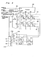
- Fig. 3 and Fig. 2 and Fig. 4 show a second embodiment of the present invention.
- Fig. 3 is a block diagram of the circuit of the present embodiment, each circuit construction to be composed of an LCD panel 10, first and second row driving portions 20 and 30, first and second column driving portions, first and second polarity reversing circuits 60 and 70, a synchronous control circuit 80 is completely the same as those of Fig. 1, with the description being omitted.
- the difference between the second embodiment and the first embodiment is that the first polarity reversing circuit (60) reverses in polarity the picture signal for each one frame with the control signal from the synchronous control circuit (80), reverses it in polarity for each one horizontal scanning period (1H).
- Figs. 2(a) through 2(d) show the driving waveforms to be applied upon the respective picture elements a, b, c, d of Fig. 3,
- Figs. 2(e) through 2(h) show the brilliance of each picture element.
- the flickers are caused with each picture element of four in the two-frame period, but the visual brilliance of Fig. 2(i) composes the brilliance of each picture element when four picture elements are regarded as one on the whole, the period of the flicker becomes one field to increase the frequency so that the flickers become substantially inconspicuous.
- Fig. 4 is the other waveform chart showing the operation of the driving circuit of Fig. 3.
- Vv is a video signal reversed in polarity for each 1H and for 1 frame.
- VG 1 , VG 2 ... VGN are gate signals to be applied upon the gate electrode lines (G), (G) ... of each electrode corresponding to the odd-numbered field,
- VP 1 , VP 21 ... VPN are volts to be retained by the liquid crystals of the respective columns corresponding to the odd-numbered field.
- the voltage of the video signal (Vv) sampled at the gate signal (VG 1 ) high timing in the 1H th in the odd-numbered field is applied upon the liquid crystal, the gate signal tries to be retained during the 1 frame period after it has become low, the charging and discharging operations are performed to the source electrode line through the off resistor of the TFT as described hereinbefore so that the holding voltage becomes like VP 1 .
- the amount of the charging and discharge operation in the one frame depends upon the voltage of the video signal of the source electrode line, but the video signal reverses for each 1H so that the average voltage of the source electrode line in one frame becomes almost the same even in any portion of the picture face. Accordingly, the retaining voltages VP 1 , VP 21 ... VPN respectively become the same charging and discharging amount as shown. This may be said likewise even in the even-numbered field.
- the hint at this time is in that the video signal is opposite in polarity to the former case when the same picture element is driven after one frame.
- the flickers through the AC driving of the adjacent picture elements are mutually offset visually, so that the flickers of the entire picture face are hardly caused even if the flickers of the individual picture element become the frequency as low as the two-frame period.
- the polarity of the video signal is reversed for each 1H, but it may be reversed for each several Hs. Also, the polarity may be reversed for each adjacent plural picture elements.
- a liquid-crystal display apparatus characterized in that the polarity of the picture signal is reversed for one horizontal scanning period or for each of a plurality of horizontal scanning periods in a liquid-crystal display apparatus wherein the picture signals reversed in polarity at the given period are applied upon the crystal panel with a plurality of display elements thereon is newly provided, so that the brilliance is not lowered in the lower portion of the picture face, the brilliance of the even-numbered line is not lowered as compared with the odd-numbered line in the interlace system so that uniformity is almost provided even in any portion on the picture-face.
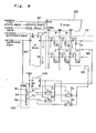
- Fig. 5 shows a third embodiment of the present invention.
- Fig. 6 through Fig. 9 respectively show the modified embodiment of Fig. 5.
- Fig. 5 is the circuit diagram of the circuit of the present embodiment, in the drawing 10 is a liquid-crystal panel of the known active matrix system, (T) shows the TFT (thin film transistor), (LC) shows the liquid-crystal.
- 20 is a Y driver which drives the respective drain lines (D), (D) of the TFT (T) which is composed of a shift register and a sample hold circuit so as to sample the picture signal with the given sampling clock.
- 40 is an X driver which is composed of a shift register and drives the respective gate lines (G), (G) ...
- the data is set by one bit with the vertical synchronous signal, is shifted with the horizontal synchronous signal to sequentially select the given gate line to feed to the TFT (T), (T) ... the signal held by the Y driver.
- T-FF T-flip-flop
- a brilliance level adjusting circuit which is composed of a first resistor (R 1 ) connected between the DC power supply (+ VDD) and the earth, a variable resistor (VR) and a second resistor (R 2 ), the connection point (a first connection point) (P 1 ) between the first resistor (R1) and the variable resistor (VR) is connected with the first analog switch (S 1 ), the connection point (a second connection point) (P 2 ) between the variable resistor (VR) and the second resistor (R 2 ) is connected with the second analog switch (S 2 ).
- the first and second analog switch outputs are connected with the opposite electrode line 90 of the liquid crystals (LC), (LC) ... and the third and fourth analog switch outputs are connected with the opposite electrode line (91).
- 60 is a polarity reversing circuit which reverses the picture signal in polarity at the field period with the control signal such as vertical synchronous signal or the like.
- first and fourth analog switches (S1) and (S 4 ) are on in the odd-numbered field and are off in the even-numbered field
- second and third analog switches (S 2 ) and (S 3 ) are off in the odd-numbered field and are on in the even-numbered field so as to perform the opening and closing operations.
- VH high voltage
- the high voltage (VH) of the first connection point (P 1 ) of the brilliance level adjusting circuit 110 is applied upon the opposite electrode line (90) in the odd-numbered field as shown in Fig.
- the picture signal is reversed at the field period by the polarity reversing circuit (6) and the level is set between VH and VL as shown in Fig. 10.
- the adjusting operation is required so that the resistance value of the variable resistor (VR) may be increased. Namely, the voltage (VH) of the first connection point (P1) becomes higher, the voltage (VL) of the second connection point (P 2 ) becomes lower so that in Fig. 10, the voltage between the opposite electrode level and the picture signal level becomes larger and the brilliance becomes higher.
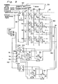
- Fig. 5 shows the line-switching one
- Fig 6 shows the dot-switching one
- Fig. 7 shows both the line-, dot-switching one
- Fig. 8 shows the line-switching one at a full line
- Fig. 9 shows both the line-, dot-switching one at a full line
- the present invention newly provides the driving circuit for the liquid-crystal display apparatus, which is composed of a liquid-crystal panel with a plurality of display elements being arranged in columns and rows thereon, a polarity reversion circuit for reversing for each field the polarity of the picture signal to be applied upon the liquid-crystal panel, a circuit for feeding the first or second DC voltage selected for each field to the opposite electrode of the liquid-crystal panel, and a brilliance level adjusting circuit for simultaneously mutually varying in the opposite direction the first and second DC voltages to adjust the brilliance level of the picture signal, so that the brilliance of the picture signals may be adjusted very simply, the power-supply voltage will become half as much as that in the conventional example, thus realizing a small-sized liquid crystal TV of higher brilliance and lower power consumption.
Abstract
Description
- The present invention relates to a liquid-crystal display apparatus using a liquid-crystal matrix panel, and particularly to the driving circuit.
- In recent years, the development of the liquid-crystal television of a portable type using the liquid-crystal matrix panel is actively performed, the details are introduced at page 211 through
page 240 of, for example, "Nikkei Electronic No. 351" (issued September 10, 1984). - One example of the electrode circuit diagram of the active matrix panel using TFT (thin film transistor) in the liquid-crystal television is shown in Fig. 11. (1), (1) ... in Fig. 11 are segment electrodes formed on the first base plate, (2) , (2) ... are the TFT (thin film transistor) formed on the first base plate, corresponding to the respective segment electrodes (1), (1) ..., are connected with the segment electrodes (1), (1) ... corresponding to the sources of the TFT (2), (2) .... (3), (3) ... are drain lines connected with the drains for each of the rows of the TFT (2), (2) ... corresponding to the segment electrodes (1), (1) ... of the row direction, (4), (4) ... are gate lines connected with the gates for each of the columns of the TFT (2), (2) corresponding to the segment electrodes (1), (1) ... of the column direction.
- On the one hand, (5) is a common electrode formed on the second base plate opposite to the first base plate with each of the segment electrodes (1), (1) ..., the TFT (2), (2) ..., the drain lines (3), (3) ..., the gate lines (4), (4) ... being formed thereon, the liquid crystal is filled between the first, second base plates.
- Also, the number of the columns, i.e., the number of the gate lines (4), (4) is 240, corresponds to approximately the number of the effective scanning lines among the number of the scanning lines 262.5 of one field of the NISC system.
- Thus, all the 250 are used respectively in the odd-number field and the even-number field during the driving operation, the same element is driven after 1/60 seconds.
- And picture signals are applied upon the drain lines (3), (3) of the active matrix panel, and when the liquid crystal is normally driven, the AC driving is preferable, namely, the polarity of the signal is desired to be inverted at a given period through the consideration of the durability or the like when the liquid crystal is normally driven, with the picture signal becoming like, for example, Fig. 12.
- Namely, assume that the nth of the odd-number field is On, the nth of the even-number field is En, the polarity is reversed for each of the fields as the odd-number fields (01), (02) become positive in polarity, the even-number fields (E1), (E2) become negative in polarity.
- Thus, the period by which the' same element is driven by the same polarity becomes 1/30 seconds, i.e., one frame period. Accordingly, the flicker (flitting) on the picture face by the polarity reversion is hardly conspicuous.
- However, in the above-described conventional example, the number of the columns is 240 with the number of the picture elements being limited, thus providing the picture face comparatively low in the resolving degree.
- Thus, the method of improving the picture quality is proposed with the number of the picture elements being increased as 480 in the number of the columns.
- The electrode circuit diagram of the active matrix panel in the second conventional embodiment is shown in Fig. 13, the same numerals are given to the same portions as those of Fig. 11 to omit the description.
- The gate lines (41), (4'2) ... in Fig. 13 are 480, are respectively taken out to left, to right for each of the columns, the gate signals are applied upon the gate line (41) ... in the odd-number field, the gate signals are applied upon the gate line (42) ... in the even-number field.
- And the picture signals to be applied upon the drain lines (3), (3) of the active matrix panel are reversed in polarity for each two-fields as shown in Fig. 14, so that the period by which the same element is driven by the same polarity becomes 1/15 seconds, namely, the two-frame period.
- Thus, the flickers on the picture face by the polarity reversion became low in the frequency, which was a very conspicuous defect.
- It is to be noted that the flickers are caused at the one-frame period as shown in Fig. 15(b) with respect to the driving waveform of the two-frame period shown in Fig. 15(a) when the LCD panel (1) is seen from the front face, but the brilliance is reduced as shown in Fig. 15(c) in a case where 10° is deviated from, for example, the front face when the LCD panel (1) is obliquely seen, the period of the flicker becomes also the two-frame period to make the flicker more conspicuous.
- The present invention is provided to improve the disadvantages of the above-described conventional examples, an object of the present invention is to increase the number. of the columns of the color matrix display apparatus from, for example, 240 to 480 to increase the number of the picture elements so that the flickers on the picture face through the AC driving operation of the liquid crystal is made inconspicuous. Thus, as the present invention is adapted to reverse the polarity of the picture signals to be applied for one display picture element adjacent within at least the same column or each plural-display picture elements, the flickers of the entire picture face is visually compensated by the above-described means.
- Also, the present invention is adapted to reverse the polarity of the picture signal for one horizontal scanning period or for each plural-horizontal scanning periods so that the brilliance of each portion on the picture face becomes uniform by the above-described means, also, to prevent the horizontal stripes.
- Furthermore, the present invention proposes the driving circuit of the liquid-crystal display apparatus, which is composed of a liquid-crystal panel with a plurality of display elements being arranged in columns and rows thereon, a polarity reversion circuit for reversing for each field the polarity of the picture signal to be applied upon the liquid-crystal panel, a circuit for feeding the first or second DC voltage selected for each field to the opposite electrode of said liquid-crystal panel, and a brilliance level adjusting circuit for simultaneously varying mutually in the opposite direction said first and second DC voltages to adjust the brilliance level of said picture signal, so that the brilliance level may be varied without any changes in the DC level of the picture signal through the above-described means.
- The liquid-crystal display apparatus in accordance with the present invention will be described hereinafter in detail with reference to the embodiment shown in the drawings.
- Fig. 1 is a block diagram of a driving circuit of the liquid-crystal display apparatus in one embodiment of the present invention. Fig. 2 is a waveform chart in the essential portions of Fig. 1. Fig. 3 is a block diagram of the driving circuit of the liquid-crystal display apparatus in the second embodiment of the present invention. Fig. 4 is the waveform chart in the essential portions of Fig. 2. Fig. 5 is a circuit diagram of the driving circuit of the liquid-crystal display apparatus in the third embodiment of the present invention. Fig. 6 through Fig. 9 are respectively the circuit diagrams showing the modified embodiments of Fig. 5. Fig. 10 is the waveform view showing the relationship between the opposed electrode electric potential in the circuit of Fig. 5 and the picture signal. Fig. 11 is an electrode circuit diagram of the active matrix panel of the conventional 240 columns. Fig. 12 is a picture signal waveform chart to be applied upon the panel of Fig. 11. rig. 13 is an electrode circuit diagram of the active matrix panel of the conventional 480 columns. Fig. 14 is a picture signal waveform chart to be applied upon the panel of Fig. 13. Figs. 15(a) and 15(b) are waveform charts for explaining the flickers.
- Fig. 1 and Fig. 2 show a first embodiment of the present invention.
- Fig. 1 is a block diagram of the present embodiment circuit, which is broadly composed of an
LCD panel 10, first and secondrow driving portions column driving portions polarity reversion circuits synchronous control circuit 80. - The
LCD panel 10 has a mosaic-shaped color filter opposed to the active matrix panels of 480 in the number of the columns, color unit display elements are arranged like G, R, B ... sequentially in the horizontal direction for the upper left portion. - The first and second
row driving portions second shift registers synchronous control circuit 80 are respectively fed, and first and second sample holdcircuits 22 and 23 to which the output pulse of each digit of the shift register is fed as the sampling pulse sample the picture signal outputs of the first or the secondpolarity reversing circuits - The first
column driving portion 40 is composed of a shift register which data-inputs the second start pulse (ST2) to be caused at the start of the odd-number field from thesynchronous control circuit 80, clock-inputs the horizontal synchronous pulse (HP), the respective digit outputs drive each gate line of the odd-numbered columns. Also, the secondcolumn driving portion 50 data-inputs the third start pulse CST3) to be caused at the start of the even field, clock-inputs the horizontal synchronous pulse (HP), the respective digit outputs drive each gate line of the even-numbered columns. - The first
polarity reversing circuit 60 reverses in polarity the picture signal for each one frame with the control signal from thesynchronous control circuit 80 to feed it to the firstsample hold circuit 22. - Also, the output of the first
polarity reversing circuit 60 is further reversed during all the period by the secondpolarity reversing circuit 70, the reversing outputs are fed to the secondsample hold circuit 32. - Thus, the signals to be applied upon the picture elements adjacent to the horizontal direction on the
LCD panel 10 become mutually reverse in polarity. - Furthermore, the
synchronous control circuit 80 contains the PLL circuit, is synchronous with the first start pulse (ST1), the vertical synchronous pulse (VP) synchronized with the horizontal synchronous pulse (HP), is synchronous to the second start pulse (ST2), the vertical synchronous pulse (VP) to be caused at the start of the odd-numbered field to compose the third start pulse (ST3) to be caused at the start of the even-numbered field and the clock pulse (CP) which is the frequency-division output of the VCO within the PLL circuit. - According to the above-described driving circuit, the picture elements adjacent to the horizontal direction are driven by the image signals mutually reverse in electrode, so that the flickers caused through the.AC driving of the adjacent elements are visually offset, the flittings on the whole picture face are hardly caused if the flicker of the individual picture element becomes a frequency as low as two frame periods.
- Also, Fig. 2 is a waveform chart for explaining the flickers in a case where the
LCD panel 10 is seen from the direction deviated by 10° from the front face, Figs. 2(a) through 2(d) respectively show the driving waveforms to be applied upon the picture elements ⓐ, ⓑ, ⓒ, ⓓ on theLCD panel 10, Figs. 2(e) through 2(h) show brilliance of each picture element. In this case, the flickers are caused with each picture element of four in the two-frame period, but the visual brilliance of Fig. 2(i) composes the brilliance of each picture element when four picture elements are regarded as one on the whole, the period of the flicker becomes one field to increase the frequency so that the flickers become substantially inconspicuous. - It is to be noted that in the above-described first embodiment, the polarity of the respective one picture element adjacent within at least the same column was reversed, but the polarity may be reversed for a respective plurality of adjacent picture elements.
- According to the present invention as described hereinabove, in a liquid-crystal display apparatus wherein the picture signals reversed in polarity at the given period are applied upon the liquid-crystal with a plurality of display elements being arranged in rows and columns thereon, a liquid-crystal display apparatus characterized in that the polarity of the picture signal to be applied is reversed for one or a plurality of display elements adjacent within at least the same column is newly provided, so that the number of the columns of the color LCD panel is made 500, the flickers are adapted not to be caused on the individual picture elements, through the driving operation by an interlace system.
- Also, the flickers may be visually compensated, if the frequency of the flicker of the picture element is reduced as compared with when the panel of the color LCD is seen from the front face, when it is seen obliquely.
- Fig. 3 and Fig. 2 and Fig. 4 show a second embodiment of the present invention.
- Fig. 3 is a block diagram of the circuit of the present embodiment, each circuit construction to be composed of an
LCD panel 10, first and secondrow driving portions polarity reversing circuits synchronous control circuit 80 is completely the same as those of Fig. 1, with the description being omitted. - The difference between the second embodiment and the first embodiment is that the first polarity reversing circuit (60) reverses in polarity the picture signal for each one frame with the control signal from the synchronous control circuit (80), reverses it in polarity for each one horizontal scanning period (1H). Figs. 2(a) through 2(d) show the driving waveforms to be applied upon the respective picture elements ⓐ, ⓑ, ⓒ, ⓓ of Fig. 3, Figs. 2(e) through 2(h) show the brilliance of each picture element. Even in the case of the second embodiment as in the first embodiment, the flickers are caused with each picture element of four in the two-frame period, but the visual brilliance of Fig. 2(i) composes the brilliance of each picture element when four picture elements are regarded as one on the whole, the period of the flicker becomes one field to increase the frequency so that the flickers become substantially inconspicuous.
- Fig. 4 is the other waveform chart showing the operation of the driving circuit of Fig. 3. In Fig. 4, Vv is a video signal reversed in polarity for each 1H and for 1 frame. VG1, VG2 ... VGN are gate signals to be applied upon the gate electrode lines (G), (G) ... of each electrode corresponding to the odd-numbered field, VP1, VP21 ... VPN are volts to be retained by the liquid crystals of the respective columns corresponding to the odd-numbered field.
- First, the voltage of the video signal (Vv) sampled at the gate signal (VG1) high timing in the 1H th in the odd-numbered field is applied upon the liquid crystal, the gate signal tries to be retained during the 1 frame period after it has become low, the charging and discharging operations are performed to the source electrode line through the off resistor of the TFT as described hereinbefore so that the holding voltage becomes like VP1. The amount of the charging and discharge operation in the one frame depends upon the voltage of the video signal of the source electrode line, but the video signal reverses for each 1H so that the average voltage of the source electrode line in one frame becomes almost the same even in any portion of the picture face. Accordingly, the retaining voltages VP1, VP21 ... VPN respectively become the same charging and discharging amount as shown. This may be said likewise even in the even-numbered field. The hint at this time is in that the video signal is opposite in polarity to the former case when the same picture element is driven after one frame.
- Thus, the uneven brilliance is' not caused above and below the picture face.
- Also, as the picture element adjacent to the horizontal direction is driven by the picture signals which are mutually opposite in polarity, the flickers through the AC driving of the adjacent picture elements are mutually offset visually, so that the flickers of the entire picture face are hardly caused even if the flickers of the individual picture element become the frequency as low as the two-frame period.
- In the above-described embodiment, the polarity of the video signal is reversed for each 1H, but it may be reversed for each several Hs. Also, the polarity may be reversed for each adjacent plural picture elements.
- According to the present invention as described hereinabove, a liquid-crystal display apparatus characterized in that the polarity of the picture signal is reversed for one horizontal scanning period or for each of a plurality of horizontal scanning periods in a liquid-crystal display apparatus wherein the picture signals reversed in polarity at the given period are applied upon the crystal panel with a plurality of display elements thereon is newly provided, so that the brilliance is not lowered in the lower portion of the picture face, the brilliance of the even-numbered line is not lowered as compared with the odd-numbered line in the interlace system so that uniformity is almost provided even in any portion on the picture-face.
- Fig. 5 shows a third embodiment of the present invention. Fig. 6 through Fig. 9 respectively show the modified embodiment of Fig. 5.
- Fig. 5 is the circuit diagram of the circuit of the present embodiment, in the drawing 10 is a liquid-crystal panel of the known active matrix system, (T) shows the TFT (thin film transistor), (LC) shows the liquid-crystal. 20 is a Y driver which drives the respective drain lines (D), (D) of the TFT (T) which is composed of a shift register and a sample hold circuit so as to sample the picture signal with the given sampling clock. 40 is an X driver which is composed of a shift register and drives the respective gate lines (G), (G) ... of the TFT (T), (T), the data is set by one bit with the vertical synchronous signal, is shifted with the horizontal synchronous signal to sequentially select the given gate line to feed to the TFT (T), (T) ... the signal held by the Y driver.
- 100 is a T-flip-flop (T-FF) where the output is reversed for each clock input (vertical synchronous signal), (S 1), (S 2), (S3) and (S4) are first, second, third and fourth analog switches to be controlled by the Q output and the Q output of the T-FF. 110 is a brilliance level adjusting circuit which is composed of a first resistor (R1) connected between the DC power supply (+ VDD) and the earth, a variable resistor (VR) and a second resistor (R2), the connection point (a first connection point) (P1) between the first resistor (R1) and the variable resistor (VR) is connected with the first analog switch (S1), the connection point (a second connection point) (P2) between the variable resistor (VR) and the second resistor (R2) is connected with the second analog switch (S2). And the first and second analog switch outputs are connected with the
opposite electrode line 90 of the liquid crystals (LC), (LC) ... and the third and fourth analog switch outputs are connected with the opposite electrode line (91). It is to be noted that 60 is a polarity reversing circuit which reverses the picture signal in polarity at the field period with the control signal such as vertical synchronous signal or the like. - The operation of the above-described circuit of the present embodiment will be described hereinafter.
- First, as the T-
FF 100 output reverses at the field period, for example, first and fourth analog switches (S1) and (S4) are on in the odd-numbered field and are off in the even-numbered field, and second and third analog switches (S2) and (S3) are off in the odd-numbered field and are on in the even-numbered field so as to perform the opening and closing operations. Thus, the high voltage (VH) of the first connection point (P1) of the brilliancelevel adjusting circuit 110 is applied upon the opposite electrode line (90) in the odd-numbered field as shown in Fig. 5, and the low voltage (VL) of the second connection point (P2) is applied upon the opposite electrode line (91), the voltage (VL) is applied upon the line (90) in the odd-numbered field, and the voltage (VH) is applied upon the line (91). - On one hand, the picture signal is reversed at the field period by the polarity reversing circuit (6) and the level is set between VH and VL as shown in Fig. 10.
- And when the brilliance level is changed, for example, when the brilliance is increased, the adjusting operation is required so that the resistance value of the variable resistor (VR) may be increased. Namely, the voltage (VH) of the first connection point (P1) becomes higher, the voltage (VL) of the second connection point (P2) becomes lower so that in Fig. 10, the voltage between the opposite electrode level and the picture signal level becomes larger and the brilliance becomes higher.
- Furthermore, the circuit of the above-described Fig. 5 shows the line-switching one, as the modified embodiment of Fig. 5, Fig 6 shows the dot-switching one, Fig. 7 shows both the line-, dot-switching one, Fig. 8 shows the line-switching one at a full line, Fig. 9 shows both the line-, dot-switching one at a full line, they are respectively capable of achieving the operational effects similar to that of Fig. 5.
- As described hereinabove, the present invention newly provides the driving circuit for the liquid-crystal display apparatus, which is composed of a liquid-crystal panel with a plurality of display elements being arranged in columns and rows thereon, a polarity reversion circuit for reversing for each field the polarity of the picture signal to be applied upon the liquid-crystal panel, a circuit for feeding the first or second DC voltage selected for each field to the opposite electrode of the liquid-crystal panel, and a brilliance level adjusting circuit for simultaneously mutually varying in the opposite direction the first and second DC voltages to adjust the brilliance level of the picture signal, so that the brilliance of the picture signals may be adjusted very simply, the power-supply voltage will become half as much as that in the conventional example, thus realizing a small-sized liquid crystal TV of higher brilliance and lower power consumption.
-
- (1) A liquid-crystal display apparatus comprising a liquid-crystal panel which has a plurality of display picture elements disposed in columns and rows, is driven through application of picture signals to be reversed in polarity at the given period, a first polarity reversing circuit for reversing the polarity of said picture-signal to be applied upon said liquid-crystal panel for each display element of at least one or more adjacent within at least the same column.
- (2) A liquid-crystal display apparatus comprising a liquid-crystal panel which has a plurality of display picture elements disposed in columns and rows, is driven through application of picture signals to be reversed in polarity at the given period, a second polarity reversing circuit for reversing the polarity of said picture signal to be applied upon said liquid-crystal panel for at least one horizontal scanning period or more.
- (3) A liquid-crystal display apparatus comprising a liquid-crystal panel which has a plurality of display picture elements disposed in columns and rows, is driven through application of picture signals to be reversed in polarity at the given period, a first polarity reversing circuit for reversing the polarity of said picture signal to be applied upon said liquid-crystal panel for each display element of at least one or more adjacent within at least the same column, a second polarity reversing circuit for reversing the polarity of said picture signal to be applied upon said liquid-crystal panel for at least one horizontal scanning period or more.
- (4) A driving circuit for a liquid-crystal display apparatus comprising a liquid-crystal panel which has a plurality of display picture elements disposed in columns and rows, is driven through application of picture signals to be reversed in polarity at the given period, a third polarity reversing circuit for reversing for each field the polarity of the picture signal to be applied upon said liquid-crystal panel, a circuit for feeding the first or the second DC voltage selected for each field the opposite electrode of said liquid crystal, a brilliance level adjusting circuit for simultaneously varying said first and second DC voltage mutually in the opposite direction so as to adjust the brilliance level of said picture signal.
Claims (4)
- (1) A liquid-crystal display apparatus comprising a liquid-crystal panel which has a plurality of display picture elements arranged alternatively with one column to be selected at the odd field and the other column to be selected at the even field, is driven through application of picture signals to be reversed in polarity at the field period, a first polarity reversing circuit for reversing the polarity of said picture signal to be applied upon said liquid-crystal panel for each display element of at least. one or more adjacent within at least the same column.
- (2) A liquid-crystal display apparatus comprising a liquid-crystal panel which has a plurality of display picture elements arranged alternatively with one column to be selected at the odd field and the other column to be selected at the even field, is driven through application of picture signals to be reversed in polarity at the field period, a second polarity reversing circuit for reversing the polarity of said picture signal to be applied upon said liquid-crystal panel for at least one horizontal scanning period or more.
- (3) A liquid-crystal display apparatus comprising a liquid-crystal panel which has a plurality of display picture elements arranged alternatively with one column to be selected at the odd field and the other column to be selected at the even field, is driven through application of picture signals to be reversed in polarity at the field period, a first polarity reversing circuit for reversing the polarity of said picture signal to be applied upon said liquid-crystal panel for each display element of at least one or more adjacent within at least the same column, a second polarity reversing circuit for reversing the polarity of said picture signal to be applied upon said liquid-crystal panel for at least one horizontal scanning period or more.
- (4) A driving circuit for a liquid-crystal display apparatus comprising a liquid-crystal panel which has a plurality of display picture elements disposed in columns and rows, is driven through application of picture signals to be reversed in polarity at the field period, a third polarity reversing circuit for reversing for the given period the polarity of the picture signal to be applied upon said liquid-crystal panel, a circuit for feeding the first or the second DC voltage selected for the given period the opposite electrode of said liquid crystal, a brilliance level adjusting circuit for simultaneously varying said first and second DC voltage mutually in the opposite direction so as to adjust the brilliance level of said picture signal.
Applications Claiming Priority (6)
| Application Number | Priority Date | Filing Date | Title |
|---|---|---|---|
| JP1985157970U JPS6266476U (en) | 1985-10-16 | 1985-10-16 | |
| JP157970/85 | 1985-10-16 | ||
| JP254145/85 | 1985-11-13 | ||
| JP60254145A JPS62113129A (en) | 1985-11-13 | 1985-11-13 | Driving method for liquid crystal display device |
| JP278521/85 | 1985-12-11 | ||
| JP27852185A JPH0654962B2 (en) | 1985-12-11 | 1985-12-11 | LCD drive circuit |
Publications (3)
| Publication Number | Publication Date |
|---|---|
| EP0241562A1 true EP0241562A1 (en) | 1987-10-21 |
| EP0241562A4 EP0241562A4 (en) | 1988-04-06 |
| EP0241562B1 EP0241562B1 (en) | 1992-06-24 |
Family
ID=27321264
Family Applications (1)
| Application Number | Title | Priority Date | Filing Date |
|---|---|---|---|
| EP86906432A Expired - Lifetime EP0241562B1 (en) | 1985-10-16 | 1986-10-16 | Liquid crystal display device |
Country Status (6)
| Country | Link |
|---|---|
| US (1) | US5093655A (en) |
| EP (1) | EP0241562B1 (en) |
| KR (1) | KR930008166B1 (en) |
| AU (1) | AU588062B2 (en) |
| DE (1) | DE3685821T2 (en) |
| WO (1) | WO1987002537A1 (en) |
Cited By (29)
| Publication number | Priority date | Publication date | Assignee | Title |
|---|---|---|---|---|
| EP0278778A2 (en) * | 1987-02-13 | 1988-08-17 | Seiko Instruments Inc. | An active matrix display device of the non-linear two-terminal type |
| EP0319635A1 (en) * | 1987-12-04 | 1989-06-14 | Stanley Electric Co., Ltd. | Liquid crystal television |
| EP0323260A2 (en) * | 1987-12-29 | 1989-07-05 | Sharp Kabushiki Kaisha | Drive apparatus for liquid crystal display device |
| EP0351253A2 (en) * | 1988-07-15 | 1990-01-17 | Sharp Kabushiki Kaisha | Liquid crystal projection apparatus and driving method thereof |
| EP0360523A2 (en) * | 1988-09-20 | 1990-03-28 | Nec Corporation | Active matrix liquid crystal display with reduced flicker |
| WO1990007768A1 (en) * | 1988-12-29 | 1990-07-12 | Honeywell Inc. | Flicker-free liquid crystal display driver system |
| EP0382567A2 (en) * | 1989-02-10 | 1990-08-16 | Sharp Kabushiki Kaisha | Liquid crystal display device and driving method therefor |
| EP0400993A2 (en) * | 1989-06-02 | 1990-12-05 | Matsushita Electric Works, Ltd. | Projection-type image display apparatus |
| EP0402850A2 (en) * | 1989-06-12 | 1990-12-19 | Kabushiki Kaisha Toshiba | Dot-matrix display apparatus |
| EP0428250A2 (en) * | 1989-08-31 | 1991-05-22 | Sharp Kabushiki Kaisha | Driver circuit for a display panel |
| EP0506530A1 (en) * | 1991-03-29 | 1992-09-30 | Thomson-Lcd | Matrix display with improved definition and addressing method of such a display |
| FR2681973A1 (en) * | 1991-09-27 | 1993-04-02 | Thomson Lcd | Matrix screen with electro-optical cells |
| US5283477A (en) * | 1989-08-31 | 1994-02-01 | Sharp Kabushiki Kaisha | Common driver circuit |
| WO1994010794A1 (en) * | 1992-11-04 | 1994-05-11 | Kopin Corporation | Control system for projection displays |
| FR2698202A1 (en) * | 1992-11-19 | 1994-05-20 | Lelah Alan | Electronic display screen control circuit for e.g. liquid crystal display - uses sample=hold circuits and multiplexer to control individual rows and columns of liquid crystal display |
| EP0611144A2 (en) * | 1993-02-09 | 1994-08-17 | Sharp Kabushiki Kaisha | Voltage generating circuit, and common electrode drive circuit, signal line drive circuit and gray-scale voltage generating circuit for display devices |
| WO1995001701A1 (en) * | 1993-06-30 | 1995-01-12 | Philips Electronics N.V. | Matrix display systems and methods of operating such systems |
| EP0637009A2 (en) * | 1993-07-30 | 1995-02-01 | Canon Kabushiki Kaisha | Driving method and apparatus for a colour active matrix LCD |
| EP0755044A1 (en) * | 1995-07-18 | 1997-01-22 | International Business Machines Corporation | Device and method for driving liquid crystal display with precharge pf display data lines |
| EP0767449A2 (en) | 1995-09-29 | 1997-04-09 | Sharp Kabushiki Kaisha | Method and circuit for driving active matrix liquid crystal panel with control of the average driving voltage |
| US5751261A (en) * | 1990-12-31 | 1998-05-12 | Kopin Corporation | Control system for display panels |
| EP0875881A2 (en) * | 1997-04-30 | 1998-11-04 | SHARP Corporation | Active matrix light modulators, use of an active matrix light modulator, and display |
| US6288697B1 (en) | 1996-11-15 | 2001-09-11 | Sharp Kabushiki Kaisha | Method and circuit for driving display device |
| US6320568B1 (en) | 1990-12-31 | 2001-11-20 | Kopin Corporation | Control system for display panels |
| EP1239444A1 (en) * | 2001-03-06 | 2002-09-11 | Matsushita Electric Industrial Co., Ltd. | Liquid crystal display device and method for driving the same |
| EP1628285A1 (en) * | 2004-08-20 | 2006-02-22 | Samsung SDI Co., Ltd. | Method for managing display data of a light emitting display |
| US7336249B2 (en) | 1996-03-26 | 2008-02-26 | Semiconductor Energy Laboratory Co., Ltd. | Driving method of active matrix display device |
| US8547300B2 (en) | 2004-06-30 | 2013-10-01 | Samsung Display Co., Ltd. | Light emitting display and display panel and driving method thereof |
| US9466251B2 (en) | 1997-11-17 | 2016-10-11 | Semiconductor Energy Laboratory Co., Ltd. | Picture display device and method of driving the same |
Families Citing this family (62)
| Publication number | Priority date | Publication date | Assignee | Title |
|---|---|---|---|---|
| US5182549A (en) * | 1987-03-05 | 1993-01-26 | Canon Kabushiki Kaisha | Liquid crystal apparatus |
| JP2682886B2 (en) * | 1990-04-25 | 1997-11-26 | シャープ株式会社 | Driving method of display device |
| JPH0497126A (en) * | 1990-08-16 | 1992-03-30 | Internatl Business Mach Corp <Ibm> | Liquid crystal display unit |
| JPH04113314A (en) * | 1990-09-03 | 1992-04-14 | Sharp Corp | Liquid crystal display device |
| JPH07109544B2 (en) * | 1991-05-15 | 1995-11-22 | インターナショナル・ビジネス・マシーンズ・コーポレイション | Liquid crystal display device, driving method thereof, and driving device |
| US5526014A (en) * | 1992-02-26 | 1996-06-11 | Nec Corporation | Semiconductor device for driving liquid crystal display panel |
| US5598180A (en) * | 1992-03-05 | 1997-01-28 | Kabushiki Kaisha Toshiba | Active matrix type display apparatus |
| US5731796A (en) * | 1992-10-15 | 1998-03-24 | Hitachi, Ltd. | Liquid crystal display driving method/driving circuit capable of being driven with equal voltages |
| US5781164A (en) * | 1992-11-04 | 1998-07-14 | Kopin Corporation | Matrix display systems |
| TW277129B (en) * | 1993-12-24 | 1996-06-01 | Sharp Kk | |
| TW270198B (en) | 1994-06-21 | 1996-02-11 | Hitachi Seisakusyo Kk | |
| JP2743841B2 (en) * | 1994-07-28 | 1998-04-22 | 日本電気株式会社 | Liquid crystal display |
| US5528256A (en) * | 1994-08-16 | 1996-06-18 | Vivid Semiconductor, Inc. | Power-saving circuit and method for driving liquid crystal display |
| KR0161918B1 (en) * | 1995-07-04 | 1999-03-20 | 구자홍 | Data driver of liquid crystal device |
| US5959599A (en) * | 1995-11-07 | 1999-09-28 | Semiconductor Energy Laboratory Co., Ltd. | Active matrix type liquid-crystal display unit and method of driving the same |
| TW329500B (en) | 1995-11-14 | 1998-04-11 | Handotai Energy Kenkyusho Kk | Electro-optical device |
| JP3597287B2 (en) * | 1995-11-29 | 2004-12-02 | 株式会社半導体エネルギー研究所 | Display device and driving method thereof |
| KR100228280B1 (en) * | 1995-12-30 | 1999-11-01 | 윤종용 | Display device display device driving circuit and its method |
| US5999150A (en) * | 1996-04-17 | 1999-12-07 | Northrop Grumman Corporation | Electroluminescent display having reversible voltage polarity |
| TW375696B (en) * | 1996-06-06 | 1999-12-01 | Toshiba Corp | Display device |
| KR100228282B1 (en) * | 1996-09-17 | 1999-11-01 | 윤종용 | Liquid display device |
| JP3612895B2 (en) * | 1996-10-23 | 2005-01-19 | カシオ計算機株式会社 | Liquid crystal display |
| US6545654B2 (en) | 1996-10-31 | 2003-04-08 | Kopin Corporation | Microdisplay for portable communication systems |
| JPH11161243A (en) * | 1997-09-26 | 1999-06-18 | Sharp Corp | Liquid crystal display device |
| US6366271B1 (en) * | 1997-11-13 | 2002-04-02 | Mitsubishi Denki Kabushiki Kaisha | Method for driving a liquid crystal display apparatus and driving circuit therefor |
| TW457389B (en) * | 1998-03-23 | 2001-10-01 | Toshiba Corp | Liquid crystal display element |
| US6496172B1 (en) * | 1998-03-27 | 2002-12-17 | Semiconductor Energy Laboratory Co., Ltd. | Liquid crystal display device, active matrix type liquid crystal display device, and method of driving the same |
| KR100430094B1 (en) * | 1998-08-11 | 2004-07-23 | 엘지.필립스 엘시디 주식회사 | Active Matrix Liquid Crystal Display and Method thereof |
| KR100312760B1 (en) * | 1999-02-24 | 2001-11-03 | 윤종용 | Liquid Crystal Display panel and Liquid Crystal Display device and Driving method thereof |
| US7098884B2 (en) * | 2000-02-08 | 2006-08-29 | Semiconductor Energy Laboratory Co., Ltd. | Semiconductor display device and method of driving semiconductor display device |
| US6999057B2 (en) * | 2000-02-22 | 2006-02-14 | Kopin Corporation | Timing of fields of video |
| TWI237802B (en) * | 2000-07-31 | 2005-08-11 | Semiconductor Energy Lab | Driving method of an electric circuit |
| JP3519355B2 (en) * | 2000-09-29 | 2004-04-12 | シャープ株式会社 | Driving device and driving method for liquid crystal display device |
| WO2002050603A1 (en) * | 2000-12-19 | 2002-06-27 | Matsushita Electric Industrial Co., Ltd. | Liquid crystal display and its driving method |
| JP4841083B2 (en) * | 2001-09-06 | 2011-12-21 | ルネサスエレクトロニクス株式会社 | Liquid crystal display device and signal transmission method in the liquid crystal display device |
| EP1300826A3 (en) * | 2001-10-03 | 2009-11-18 | Nec Corporation | Display device and semiconductor device |
| JP3906665B2 (en) * | 2001-10-05 | 2007-04-18 | カシオ計算機株式会社 | Liquid crystal drive device |
| KR100840316B1 (en) * | 2001-11-26 | 2008-06-20 | 삼성전자주식회사 | A Liquid Crystal Display and A Driving Method Thereof |
| JP3820379B2 (en) * | 2002-03-13 | 2006-09-13 | 松下電器産業株式会社 | Liquid crystal drive device |
| WO2003083815A2 (en) * | 2002-03-28 | 2003-10-09 | Koninklijke Philips Electronics N.V. | Liquid crystal display driving with dot-inversion |
| KR100859467B1 (en) * | 2002-04-08 | 2008-09-23 | 엘지디스플레이 주식회사 | Liquid crystal display and driving method thereof |
| DE10252166A1 (en) * | 2002-11-09 | 2004-05-19 | Philips Intellectual Property & Standards Gmbh | Matrix display with pixel selection arrangement of neighboring pixels being connected mutually with bordering control lines |
| KR100532995B1 (en) * | 2003-04-18 | 2005-12-02 | 엘지전자 주식회사 | Method for driving flat display panel |
| KR101032945B1 (en) * | 2004-03-12 | 2011-05-09 | 삼성전자주식회사 | Shift register and display device including shift register |
| KR101057891B1 (en) * | 2004-05-31 | 2011-08-19 | 엘지디스플레이 주식회사 | Shift register |
| JP2007121832A (en) * | 2005-10-31 | 2007-05-17 | Oki Electric Ind Co Ltd | Drive unit of liquid crystal display device |
| TWI298470B (en) * | 2005-12-16 | 2008-07-01 | Chi Mei Optoelectronics Corp | Flat panel display and the image-driving method thereof |
| US8643624B2 (en) * | 2009-03-18 | 2014-02-04 | Synaptics Incorporated | Capacitive sensing using a segmented common voltage electrode of a display |
| US9805692B2 (en) * | 2010-02-26 | 2017-10-31 | Synaptics Incorporated | Varying demodulation to avoid interference |
| US9898121B2 (en) | 2010-04-30 | 2018-02-20 | Synaptics Incorporated | Integrated capacitive sensing and displaying |
| CN103907085B (en) | 2011-09-07 | 2017-02-22 | 辛纳普蒂克斯公司 | Capacitive sensing during non-display update times |
| US8970547B2 (en) | 2012-02-01 | 2015-03-03 | Synaptics Incorporated | Noise-adapting touch sensing window |
| US10073568B2 (en) | 2012-08-15 | 2018-09-11 | Synaptics Incorporated | System and method for interference avoidance for a display device comprising an integrated sensing device |
| US10073550B2 (en) | 2012-09-20 | 2018-09-11 | Synaptics Incorporated | Concurrent input sensing and display updating |
| US9442615B2 (en) | 2013-10-02 | 2016-09-13 | Synaptics Incorporated | Frequency shifting for simultaneous active matrix display update and in-cell capacitive touch |
| US9582099B2 (en) | 2014-03-31 | 2017-02-28 | Synaptics Incorporated | Serrated input sensing intervals |
| US9298309B2 (en) | 2014-04-29 | 2016-03-29 | Synaptics Incorporated | Source driver touch transmitter in parallel with display drive |
| US10175827B2 (en) | 2014-12-23 | 2019-01-08 | Synaptics Incorporated | Detecting an active pen using a capacitive sensing device |
| US10394391B2 (en) | 2015-01-05 | 2019-08-27 | Synaptics Incorporated | System and method for reducing display artifacts |
| US10275070B2 (en) | 2015-01-05 | 2019-04-30 | Synaptics Incorporated | Time sharing of display and sensing data |
| US10037112B2 (en) | 2015-09-30 | 2018-07-31 | Synaptics Incorporated | Sensing an active device'S transmission using timing interleaved with display updates |
| US10592022B2 (en) | 2015-12-29 | 2020-03-17 | Synaptics Incorporated | Display device with an integrated sensing device having multiple gate driver circuits |
Citations (2)
| Publication number | Priority date | Publication date | Assignee | Title |
|---|---|---|---|---|
| GB2134300A (en) * | 1982-12-21 | 1984-08-08 | Citizen Watch Co Ltd | Drive method for active matrix display device |
| JPS603698A (en) * | 1983-06-21 | 1985-01-10 | ソニー株式会社 | Liquid crystal display |
Family Cites Families (15)
| Publication number | Priority date | Publication date | Assignee | Title |
|---|---|---|---|---|
| US4027305A (en) * | 1973-08-09 | 1977-05-31 | Canon Kabushiki Kaisha | System for driving liquid crystal display device |
| US4200868A (en) * | 1978-04-03 | 1980-04-29 | International Business Machines Corporation | Buffered high frequency plasma display system |
| JPS55129399A (en) * | 1979-03-29 | 1980-10-07 | Sony Corp | Xy matrix display unit |
| JPS56117287A (en) * | 1980-02-21 | 1981-09-14 | Sharp Kk | Indicator driving system |
| JPS56156884A (en) * | 1980-05-09 | 1981-12-03 | Hitachi Ltd | Method of driving gas discharge display element |
| JPS57201295A (en) * | 1981-06-04 | 1982-12-09 | Sony Corp | Two-dimensional address device |
| JPS5888788A (en) * | 1981-11-24 | 1983-05-26 | 株式会社日立製作所 | Liquid crystal display |
| US4525710A (en) * | 1982-02-16 | 1985-06-25 | Seiko Instruments & Electronics Ltd. | Picture display device |
| FR2524679B1 (en) * | 1982-04-01 | 1990-07-06 | Suwa Seikosha Kk | METHOD OF ATTACKING AN ACTIVE MATRIX LIQUID CRYSTAL DISPLAY PANEL |
| JPS59157693A (en) * | 1983-02-28 | 1984-09-07 | シチズン時計株式会社 | Driving of display |
| JPS59220793A (en) * | 1983-05-31 | 1984-12-12 | ソニー株式会社 | Driving of display |
| AU552858B2 (en) * | 1983-06-06 | 1986-06-26 | Stc Plc | Scanning liquid crystal dispaly cells |
| JPS6083477A (en) * | 1983-10-13 | 1985-05-11 | Sharp Corp | Driving circuit of liquid crystal display device |
| JPS61117599A (en) * | 1984-11-13 | 1986-06-04 | キヤノン株式会社 | Switching pulse for video display unit |
| GB2173629B (en) * | 1986-04-01 | 1989-11-15 | Stc Plc | Addressing liquid crystal cells |
-
1986
- 1986-10-16 AU AU65269/86A patent/AU588062B2/en not_active Ceased
- 1986-10-16 WO PCT/JP1986/000525 patent/WO1987002537A1/en active IP Right Grant
- 1986-10-16 DE DE8686906432T patent/DE3685821T2/en not_active Expired - Fee Related
- 1986-10-16 KR KR1019870700507A patent/KR930008166B1/en not_active IP Right Cessation
- 1986-10-16 EP EP86906432A patent/EP0241562B1/en not_active Expired - Lifetime
-
1991
- 1991-03-25 US US07/675,052 patent/US5093655A/en not_active Expired - Fee Related
Patent Citations (2)
| Publication number | Priority date | Publication date | Assignee | Title |
|---|---|---|---|---|
| GB2134300A (en) * | 1982-12-21 | 1984-08-08 | Citizen Watch Co Ltd | Drive method for active matrix display device |
| JPS603698A (en) * | 1983-06-21 | 1985-01-10 | ソニー株式会社 | Liquid crystal display |
Non-Patent Citations (1)
| Title |
|---|
| See also references of WO8702537A1 * |
Cited By (54)
| Publication number | Priority date | Publication date | Assignee | Title |
|---|---|---|---|---|
| EP0278778A3 (en) * | 1987-02-13 | 1991-04-10 | Seiko Instruments Inc. | An active matrix display device of the non-linear two-terminal type |
| EP0278778A2 (en) * | 1987-02-13 | 1988-08-17 | Seiko Instruments Inc. | An active matrix display device of the non-linear two-terminal type |
| EP0319635A1 (en) * | 1987-12-04 | 1989-06-14 | Stanley Electric Co., Ltd. | Liquid crystal television |
| EP0323260A2 (en) * | 1987-12-29 | 1989-07-05 | Sharp Kabushiki Kaisha | Drive apparatus for liquid crystal display device |
| EP0597828A2 (en) * | 1987-12-29 | 1994-05-18 | SHARP Corporation | Video signal field for discriminating device, e.g. for a liquid crystal display |
| EP0323260A3 (en) * | 1987-12-29 | 1990-10-24 | Sharp Kabushiki Kaisha | Drive apparatus for liquid crystal display device |
| EP0597828A3 (en) * | 1987-12-29 | 1994-08-24 | Sharp Kk | Video signal field for discriminating device, e.g. for a liquid crystal display. |
| EP0351253A2 (en) * | 1988-07-15 | 1990-01-17 | Sharp Kabushiki Kaisha | Liquid crystal projection apparatus and driving method thereof |
| US5122790A (en) * | 1988-07-15 | 1992-06-16 | Sharp Kabushiki Kaisha | Liquid crystal projection apparatus and driving method thereof |
| EP0351253A3 (en) * | 1988-07-15 | 1991-04-24 | Sharp Kabushiki Kaisha | Liquid crystal projection apparatus and driving method thereof |
| EP0360523A2 (en) * | 1988-09-20 | 1990-03-28 | Nec Corporation | Active matrix liquid crystal display with reduced flicker |
| EP0360523A3 (en) * | 1988-09-20 | 1991-08-14 | Nec Corporation | Active matrix liquid crystal display with reduced flicker |
| US5041823A (en) * | 1988-12-29 | 1991-08-20 | Honeywell Inc. | Flicker-free liquid crystal display driver system |
| WO1990007768A1 (en) * | 1988-12-29 | 1990-07-12 | Honeywell Inc. | Flicker-free liquid crystal display driver system |
| US5365284A (en) * | 1989-02-10 | 1994-11-15 | Sharp Kabushiki Kaisha | Liquid crystal display device and driving method thereof |
| EP0382567B1 (en) * | 1989-02-10 | 1996-05-29 | Sharp Kabushiki Kaisha | Liquid crystal display device and driving method therefor |
| EP0382567A2 (en) * | 1989-02-10 | 1990-08-16 | Sharp Kabushiki Kaisha | Liquid crystal display device and driving method therefor |
| EP0400993A2 (en) * | 1989-06-02 | 1990-12-05 | Matsushita Electric Works, Ltd. | Projection-type image display apparatus |
| EP0400993A3 (en) * | 1989-06-02 | 1991-10-02 | Matsushita Electric Works, Ltd. | Projection-type image display apparatus |
| EP0402850A3 (en) * | 1989-06-12 | 1991-10-23 | Kabushiki Kaisha Toshiba | Dot-matrix display apparatus |
| US5241304A (en) * | 1989-06-12 | 1993-08-31 | Kabushiki Kaisha Toshiba | Dot-matrix display apparatus |
| EP0402850A2 (en) * | 1989-06-12 | 1990-12-19 | Kabushiki Kaisha Toshiba | Dot-matrix display apparatus |
| US5283477A (en) * | 1989-08-31 | 1994-02-01 | Sharp Kabushiki Kaisha | Common driver circuit |
| EP0428250A3 (en) * | 1989-08-31 | 1992-07-01 | Sharp Kabushiki Kaisha | Common driver circuit for a display panel |
| EP0428250A2 (en) * | 1989-08-31 | 1991-05-22 | Sharp Kabushiki Kaisha | Driver circuit for a display panel |
| US6320568B1 (en) | 1990-12-31 | 2001-11-20 | Kopin Corporation | Control system for display panels |
| US6121950A (en) * | 1990-12-31 | 2000-09-19 | Kopin Corporation | Control system for display panels |
| US5751261A (en) * | 1990-12-31 | 1998-05-12 | Kopin Corporation | Control system for display panels |
| FR2674663A1 (en) * | 1991-03-29 | 1992-10-02 | Thomson Lcd | MATRIX SCREEN WITH IMPROVED DEFINITION AND METHOD FOR ADDRESSING SUCH SCREEN. |
| EP0506530A1 (en) * | 1991-03-29 | 1992-09-30 | Thomson-Lcd | Matrix display with improved definition and addressing method of such a display |
| FR2681973A1 (en) * | 1991-09-27 | 1993-04-02 | Thomson Lcd | Matrix screen with electro-optical cells |
| WO1994010794A1 (en) * | 1992-11-04 | 1994-05-11 | Kopin Corporation | Control system for projection displays |
| FR2698202A1 (en) * | 1992-11-19 | 1994-05-20 | Lelah Alan | Electronic display screen control circuit for e.g. liquid crystal display - uses sample=hold circuits and multiplexer to control individual rows and columns of liquid crystal display |
| EP0606785A1 (en) * | 1992-11-19 | 1994-07-20 | France Telecom | Colomns driving circuit for a display screen |
| EP0611144A2 (en) * | 1993-02-09 | 1994-08-17 | Sharp Kabushiki Kaisha | Voltage generating circuit, and common electrode drive circuit, signal line drive circuit and gray-scale voltage generating circuit for display devices |
| EP0611144B1 (en) * | 1993-02-09 | 2005-09-28 | Sharp Kabushiki Kaisha | Voltage generating circuit, and common electrode drive circuit, signal line drive circuit and gray-scale voltage generating circuit for display devices |
| WO1995001701A1 (en) * | 1993-06-30 | 1995-01-12 | Philips Electronics N.V. | Matrix display systems and methods of operating such systems |
| US5912651A (en) * | 1993-06-30 | 1999-06-15 | U.S. Philips Corporation | Matrix display systems and methods of operating such systems |
| EP0637009A3 (en) * | 1993-07-30 | 1997-03-19 | Canon Kk | Driving method and apparatus for a colour active matrix LCD. |
| EP0637009A2 (en) * | 1993-07-30 | 1995-02-01 | Canon Kabushiki Kaisha | Driving method and apparatus for a colour active matrix LCD |
| EP0755044A1 (en) * | 1995-07-18 | 1997-01-22 | International Business Machines Corporation | Device and method for driving liquid crystal display with precharge pf display data lines |
| EP0767449A3 (en) * | 1995-09-29 | 1998-03-18 | Sharp Kabushiki Kaisha | Method and circuit for driving active matrix liquid crystal panel with control of the average driving voltage |
| US6118421A (en) * | 1995-09-29 | 2000-09-12 | Sharp Kabushiki Kaisha | Method and circuit for driving liquid crystal panel |
| EP0767449A2 (en) | 1995-09-29 | 1997-04-09 | Sharp Kabushiki Kaisha | Method and circuit for driving active matrix liquid crystal panel with control of the average driving voltage |
| US7336249B2 (en) | 1996-03-26 | 2008-02-26 | Semiconductor Energy Laboratory Co., Ltd. | Driving method of active matrix display device |
| US6288697B1 (en) | 1996-11-15 | 2001-09-11 | Sharp Kabushiki Kaisha | Method and circuit for driving display device |
| EP0875881A3 (en) * | 1997-04-30 | 2000-03-01 | Sharp Kabushiki Kaisha | Active matrix light modulators, use of an active matrix light modulator, and display |
| EP0875881A2 (en) * | 1997-04-30 | 1998-11-04 | SHARP Corporation | Active matrix light modulators, use of an active matrix light modulator, and display |
| US9466251B2 (en) | 1997-11-17 | 2016-10-11 | Semiconductor Energy Laboratory Co., Ltd. | Picture display device and method of driving the same |
| EP1239444A1 (en) * | 2001-03-06 | 2002-09-11 | Matsushita Electric Industrial Co., Ltd. | Liquid crystal display device and method for driving the same |
| US8547300B2 (en) | 2004-06-30 | 2013-10-01 | Samsung Display Co., Ltd. | Light emitting display and display panel and driving method thereof |
| EP1628285A1 (en) * | 2004-08-20 | 2006-02-22 | Samsung SDI Co., Ltd. | Method for managing display data of a light emitting display |
| CN100388341C (en) * | 2004-08-20 | 2008-05-14 | 三星Sdi株式会社 | Method for managing display memory data of light emitting display |
| US8154481B2 (en) | 2004-08-20 | 2012-04-10 | Samsung Mobile Display Co., Ltd. | Method for managing display memory data of light emitting display |
Also Published As
| Publication number | Publication date |
|---|---|
| DE3685821T2 (en) | 1993-02-11 |
| KR880700589A (en) | 1988-03-15 |
| US5093655A (en) | 1992-03-03 |
| DE3685821D1 (en) | 1992-07-30 |
| KR930008166B1 (en) | 1993-08-26 |
| EP0241562A4 (en) | 1988-04-06 |
| AU6526986A (en) | 1987-05-05 |
| AU588062B2 (en) | 1989-09-07 |
| EP0241562B1 (en) | 1992-06-24 |
| WO1987002537A1 (en) | 1987-04-23 |
Similar Documents
| Publication | Publication Date | Title |
|---|---|---|
| US5093655A (en) | Liquid-crystal display apparatus | |
| US4804951A (en) | Display apparatus and driving method therefor | |
| KR0147917B1 (en) | Lcd with reduced power dissipation and/or reduced vertical striped shades in frame control and control method for the same | |
| US5253091A (en) | Liquid crystal display having reduced flicker | |
| CA2055877C (en) | Liquid crystal apparatus and method of driving the same | |
| US7525527B2 (en) | Method for driving a liquid crystal display device | |
| TW201003625A (en) | Liquid crystal display module | |
| US20050062707A1 (en) | Matrix addressing method and circuit, and liquid crystal display device | |
| KR20020088859A (en) | Liquid Crystal Display and Driving Method Thereof | |
| EP1410374B1 (en) | Display driver apparatus and driving method | |
| JP3055620B2 (en) | Liquid crystal display device and driving method thereof | |
| KR20070068773A (en) | Liquid crystal display | |
| KR101308442B1 (en) | LCD and drive method thereof | |
| KR100965587B1 (en) | The liquid crystal display device and the method for driving the same | |
| KR100878235B1 (en) | Liquid crystal display and driving method the same | |
| JPH08248929A (en) | Liquid crystal display device | |
| JPH05313608A (en) | Driving device of liquid crystal display panel | |
| JP4278215B2 (en) | Liquid crystal display device and driving method of liquid crystal display device | |
| JPH0430683A (en) | Liquid crystal display device | |
| JPS63287829A (en) | Electrooptical device | |
| JPH0654962B2 (en) | LCD drive circuit | |
| CN113674672B (en) | Display panel driving method and display panel | |
| JPH071621Y2 (en) | Liquid crystal display | |
| KR20010023722A (en) | Matrix display device adapted to display video signals from different video standards | |
| JPH0532829Y2 (en) |
Legal Events
| Date | Code | Title | Description |
|---|---|---|---|
| PUAI | Public reference made under article 153(3) epc to a published international application that has entered the european phase |
Free format text: ORIGINAL CODE: 0009012 |
|
| AK | Designated contracting states |
Kind code of ref document: A1 Designated state(s): DE FR GB |
|
| 17P | Request for examination filed |
Effective date: 19870909 |
|
| A4 | Supplementary search report drawn up and despatched |
Effective date: 19880406 |
|
| 17Q | First examination report despatched |
Effective date: 19900426 |
|
| GRAA | (expected) grant |
Free format text: ORIGINAL CODE: 0009210 |
|
| AK | Designated contracting states |
Kind code of ref document: B1 Designated state(s): DE FR GB |
|
| REF | Corresponds to: |
Ref document number: 3685821 Country of ref document: DE Date of ref document: 19920730 |
|
| ET | Fr: translation filed | ||
| PLBE | No opposition filed within time limit |
Free format text: ORIGINAL CODE: 0009261 |
|
| STAA | Information on the status of an ep patent application or granted ep patent |
Free format text: STATUS: NO OPPOSITION FILED WITHIN TIME LIMIT |
|
| 26N | No opposition filed | ||
| REG | Reference to a national code |
Ref country code: GB Ref legal event code: IF02 |
|
| PGFP | Annual fee paid to national office [announced via postgrant information from national office to epo] |
Ref country code: FR Payment date: 20021008 Year of fee payment: 17 |
|
| PGFP | Annual fee paid to national office [announced via postgrant information from national office to epo] |
Ref country code: GB Payment date: 20021016 Year of fee payment: 17 |
|
| PGFP | Annual fee paid to national office [announced via postgrant information from national office to epo] |
Ref country code: DE Payment date: 20021017 Year of fee payment: 17 |
|
| PG25 | Lapsed in a contracting state [announced via postgrant information from national office to epo] |
Ref country code: GB Free format text: LAPSE BECAUSE OF NON-PAYMENT OF DUE FEES Effective date: 20031016 |
|
| PG25 | Lapsed in a contracting state [announced via postgrant information from national office to epo] |
Ref country code: DE Free format text: LAPSE BECAUSE OF NON-PAYMENT OF DUE FEES Effective date: 20040501 |
|
| GBPC | Gb: european patent ceased through non-payment of renewal fee |
Effective date: 20031016 |
|
| PG25 | Lapsed in a contracting state [announced via postgrant information from national office to epo] |
Ref country code: FR Free format text: LAPSE BECAUSE OF NON-PAYMENT OF DUE FEES Effective date: 20040630 |
|
| REG | Reference to a national code |
Ref country code: FR Ref legal event code: ST |