EP0241059A2 - Method for manufacturing a power mos transistor - Google Patents
Method for manufacturing a power mos transistor Download PDFInfo
- Publication number
- EP0241059A2 EP0241059A2 EP87200388A EP87200388A EP0241059A2 EP 0241059 A2 EP0241059 A2 EP 0241059A2 EP 87200388 A EP87200388 A EP 87200388A EP 87200388 A EP87200388 A EP 87200388A EP 0241059 A2 EP0241059 A2 EP 0241059A2
- Authority
- EP
- European Patent Office
- Prior art keywords
- semiconductor region
- forming
- layer
- gate
- region
- Prior art date
- Legal status (The legal status is an assumption and is not a legal conclusion. Google has not performed a legal analysis and makes no representation as to the accuracy of the status listed.)
- Withdrawn
Links
- 238000000034 method Methods 0.000 title claims abstract description 53
- 238000004519 manufacturing process Methods 0.000 title claims abstract description 14
- VYPSYNLAJGMNEJ-UHFFFAOYSA-N Silicium dioxide Chemical compound O=[Si]=O VYPSYNLAJGMNEJ-UHFFFAOYSA-N 0.000 claims abstract description 85
- 239000004065 semiconductor Substances 0.000 claims abstract description 82
- 235000012239 silicon dioxide Nutrition 0.000 claims abstract description 42
- 239000000377 silicon dioxide Substances 0.000 claims abstract description 42
- 229910021420 polycrystalline silicon Inorganic materials 0.000 claims abstract description 31
- 210000000746 body region Anatomy 0.000 claims abstract description 26
- 238000009413 insulation Methods 0.000 claims abstract description 15
- 230000000873 masking effect Effects 0.000 claims abstract description 11
- 229910052581 Si3N4 Inorganic materials 0.000 claims description 24
- HQVNEWCFYHHQES-UHFFFAOYSA-N silicon nitride Chemical compound N12[Si]34N5[Si]62N3[Si]51N64 HQVNEWCFYHHQES-UHFFFAOYSA-N 0.000 claims description 24
- 238000005530 etching Methods 0.000 claims description 8
- 239000012535 impurity Substances 0.000 claims description 7
- 229910052751 metal Inorganic materials 0.000 claims description 6
- 239000002184 metal Substances 0.000 claims description 6
- 239000004020 conductor Substances 0.000 claims 1
- 239000000758 substrate Substances 0.000 abstract description 23
- 238000002161 passivation Methods 0.000 abstract description 4
- 229920002120 photoresistant polymer Polymers 0.000 description 9
- NBIIXXVUZAFLBC-UHFFFAOYSA-N Phosphoric acid Chemical compound OP(O)(O)=O NBIIXXVUZAFLBC-UHFFFAOYSA-N 0.000 description 8
- XUIMIQQOPSSXEZ-UHFFFAOYSA-N Silicon Chemical compound [Si] XUIMIQQOPSSXEZ-UHFFFAOYSA-N 0.000 description 6
- 238000001020 plasma etching Methods 0.000 description 6
- 239000002019 doping agent Substances 0.000 description 5
- 239000000463 material Substances 0.000 description 5
- 229910000147 aluminium phosphate Inorganic materials 0.000 description 4
- 239000007943 implant Substances 0.000 description 4
- 229910052710 silicon Inorganic materials 0.000 description 4
- 239000010703 silicon Substances 0.000 description 4
- 229910052782 aluminium Inorganic materials 0.000 description 3
- XAGFODPZIPBFFR-UHFFFAOYSA-N aluminium Chemical compound [Al] XAGFODPZIPBFFR-UHFFFAOYSA-N 0.000 description 3
- 229910052796 boron Inorganic materials 0.000 description 3
- -1 boron ions Chemical class 0.000 description 3
- 150000002500 ions Chemical class 0.000 description 3
- 238000005229 chemical vapour deposition Methods 0.000 description 2
- 238000009792 diffusion process Methods 0.000 description 2
- 238000005468 ion implantation Methods 0.000 description 2
- ZOXJGFHDIHLPTG-UHFFFAOYSA-N Boron Chemical compound [B] ZOXJGFHDIHLPTG-UHFFFAOYSA-N 0.000 description 1
- 229910045601 alloy Inorganic materials 0.000 description 1
- 239000000956 alloy Substances 0.000 description 1
- 229910052785 arsenic Inorganic materials 0.000 description 1
- 230000015572 biosynthetic process Effects 0.000 description 1
- 230000015556 catabolic process Effects 0.000 description 1
- 238000000151 deposition Methods 0.000 description 1
- BHEPBYXIRTUNPN-UHFFFAOYSA-N hydridophosphorus(.) (triplet) Chemical compound [PH] BHEPBYXIRTUNPN-UHFFFAOYSA-N 0.000 description 1
- 238000012986 modification Methods 0.000 description 1
- 230000004048 modification Effects 0.000 description 1
- 150000004767 nitrides Chemical class 0.000 description 1
- 230000003647 oxidation Effects 0.000 description 1
- 238000007254 oxidation reaction Methods 0.000 description 1
- 239000003870 refractory metal Substances 0.000 description 1
- 229910021332 silicide Inorganic materials 0.000 description 1
- FVBUAEGBCNSCDD-UHFFFAOYSA-N silicide(4-) Chemical compound [Si-4] FVBUAEGBCNSCDD-UHFFFAOYSA-N 0.000 description 1
- 239000007787 solid Substances 0.000 description 1
- 238000000992 sputter etching Methods 0.000 description 1
- XLYOFNOQVPJJNP-UHFFFAOYSA-N water Substances O XLYOFNOQVPJJNP-UHFFFAOYSA-N 0.000 description 1
Images


Classifications
-
- H—ELECTRICITY
- H01—ELECTRIC ELEMENTS
- H01L—SEMICONDUCTOR DEVICES NOT COVERED BY CLASS H10
- H01L29/00—Semiconductor devices adapted for rectifying, amplifying, oscillating or switching, or capacitors or resistors with at least one potential-jump barrier or surface barrier, e.g. PN junction depletion layer or carrier concentration layer; Details of semiconductor bodies or of electrodes thereof ; Multistep manufacturing processes therefor
- H01L29/66—Types of semiconductor device ; Multistep manufacturing processes therefor
- H01L29/66007—Multistep manufacturing processes
- H01L29/66075—Multistep manufacturing processes of devices having semiconductor bodies comprising group 14 or group 13/15 materials
- H01L29/66227—Multistep manufacturing processes of devices having semiconductor bodies comprising group 14 or group 13/15 materials the devices being controllable only by the electric current supplied or the electric potential applied, to an electrode which does not carry the current to be rectified, amplified or switched, e.g. three-terminal devices
- H01L29/66409—Unipolar field-effect transistors
- H01L29/66477—Unipolar field-effect transistors with an insulated gate, i.e. MISFET
- H01L29/66674—DMOS transistors, i.e. MISFETs with a channel accommodating body or base region adjoining a drain drift region
- H01L29/66712—Vertical DMOS transistors, i.e. VDMOS transistors
-
- H—ELECTRICITY
- H01—ELECTRIC ELEMENTS
- H01L—SEMICONDUCTOR DEVICES NOT COVERED BY CLASS H10
- H01L21/00—Processes or apparatus adapted for the manufacture or treatment of semiconductor or solid state devices or of parts thereof
- H01L21/70—Manufacture or treatment of devices consisting of a plurality of solid state components formed in or on a common substrate or of parts thereof; Manufacture of integrated circuit devices or of parts thereof
- H01L21/71—Manufacture of specific parts of devices defined in group H01L21/70
- H01L21/768—Applying interconnections to be used for carrying current between separate components within a device comprising conductors and dielectrics
- H01L21/76897—Formation of self-aligned vias or contact plugs, i.e. involving a lithographically uncritical step
-
- H—ELECTRICITY
- H01—ELECTRIC ELEMENTS
- H01L—SEMICONDUCTOR DEVICES NOT COVERED BY CLASS H10
- H01L29/00—Semiconductor devices adapted for rectifying, amplifying, oscillating or switching, or capacitors or resistors with at least one potential-jump barrier or surface barrier, e.g. PN junction depletion layer or carrier concentration layer; Details of semiconductor bodies or of electrodes thereof ; Multistep manufacturing processes therefor
- H01L29/40—Electrodes ; Multistep manufacturing processes therefor
- H01L29/402—Field plates
-
- H—ELECTRICITY
- H01—ELECTRIC ELEMENTS
- H01L—SEMICONDUCTOR DEVICES NOT COVERED BY CLASS H10
- H01L29/00—Semiconductor devices adapted for rectifying, amplifying, oscillating or switching, or capacitors or resistors with at least one potential-jump barrier or surface barrier, e.g. PN junction depletion layer or carrier concentration layer; Details of semiconductor bodies or of electrodes thereof ; Multistep manufacturing processes therefor
- H01L29/40—Electrodes ; Multistep manufacturing processes therefor
- H01L29/43—Electrodes ; Multistep manufacturing processes therefor characterised by the materials of which they are formed
- H01L29/49—Metal-insulator-semiconductor electrodes, e.g. gates of MOSFET
- H01L29/51—Insulating materials associated therewith
- H01L29/511—Insulating materials associated therewith with a compositional variation, e.g. multilayer structures
- H01L29/513—Insulating materials associated therewith with a compositional variation, e.g. multilayer structures the variation being perpendicular to the channel plane
-
- H—ELECTRICITY
- H01—ELECTRIC ELEMENTS
- H01L—SEMICONDUCTOR DEVICES NOT COVERED BY CLASS H10
- H01L29/00—Semiconductor devices adapted for rectifying, amplifying, oscillating or switching, or capacitors or resistors with at least one potential-jump barrier or surface barrier, e.g. PN junction depletion layer or carrier concentration layer; Details of semiconductor bodies or of electrodes thereof ; Multistep manufacturing processes therefor
- H01L29/66—Types of semiconductor device ; Multistep manufacturing processes therefor
- H01L29/66007—Multistep manufacturing processes
- H01L29/66075—Multistep manufacturing processes of devices having semiconductor bodies comprising group 14 or group 13/15 materials
- H01L29/66227—Multistep manufacturing processes of devices having semiconductor bodies comprising group 14 or group 13/15 materials the devices being controllable only by the electric current supplied or the electric potential applied, to an electrode which does not carry the current to be rectified, amplified or switched, e.g. three-terminal devices
- H01L29/66234—Bipolar junction transistors [BJT]
- H01L29/66325—Bipolar junction transistors [BJT] controlled by field-effect, e.g. insulated gate bipolar transistors [IGBT]
- H01L29/66333—Vertical insulated gate bipolar transistors
-
- H—ELECTRICITY
- H01—ELECTRIC ELEMENTS
- H01L—SEMICONDUCTOR DEVICES NOT COVERED BY CLASS H10
- H01L29/00—Semiconductor devices adapted for rectifying, amplifying, oscillating or switching, or capacitors or resistors with at least one potential-jump barrier or surface barrier, e.g. PN junction depletion layer or carrier concentration layer; Details of semiconductor bodies or of electrodes thereof ; Multistep manufacturing processes therefor
- H01L29/66—Types of semiconductor device ; Multistep manufacturing processes therefor
- H01L29/68—Types of semiconductor device ; Multistep manufacturing processes therefor controllable by only the electric current supplied, or only the electric potential applied, to an electrode which does not carry the current to be rectified, amplified or switched
- H01L29/76—Unipolar devices, e.g. field effect transistors
- H01L29/772—Field effect transistors
- H01L29/78—Field effect transistors with field effect produced by an insulated gate
- H01L29/7801—DMOS transistors, i.e. MISFETs with a channel accommodating body or base region adjoining a drain drift region
- H01L29/7802—Vertical DMOS transistors, i.e. VDMOS transistors
- H01L29/7811—Vertical DMOS transistors, i.e. VDMOS transistors with an edge termination structure
-
- H—ELECTRICITY
- H01—ELECTRIC ELEMENTS
- H01L—SEMICONDUCTOR DEVICES NOT COVERED BY CLASS H10
- H01L29/00—Semiconductor devices adapted for rectifying, amplifying, oscillating or switching, or capacitors or resistors with at least one potential-jump barrier or surface barrier, e.g. PN junction depletion layer or carrier concentration layer; Details of semiconductor bodies or of electrodes thereof ; Multistep manufacturing processes therefor
- H01L29/02—Semiconductor bodies ; Multistep manufacturing processes therefor
- H01L29/06—Semiconductor bodies ; Multistep manufacturing processes therefor characterised by their shape; characterised by the shapes, relative sizes, or dispositions of the semiconductor regions ; characterised by the concentration or distribution of impurities within semiconductor regions
- H01L29/0603—Semiconductor bodies ; Multistep manufacturing processes therefor characterised by their shape; characterised by the shapes, relative sizes, or dispositions of the semiconductor regions ; characterised by the concentration or distribution of impurities within semiconductor regions characterised by particular constructional design considerations, e.g. for preventing surface leakage, for controlling electric field concentration or for internal isolations regions
- H01L29/0607—Semiconductor bodies ; Multistep manufacturing processes therefor characterised by their shape; characterised by the shapes, relative sizes, or dispositions of the semiconductor regions ; characterised by the concentration or distribution of impurities within semiconductor regions characterised by particular constructional design considerations, e.g. for preventing surface leakage, for controlling electric field concentration or for internal isolations regions for preventing surface leakage or controlling electric field concentration
- H01L29/0611—Semiconductor bodies ; Multistep manufacturing processes therefor characterised by their shape; characterised by the shapes, relative sizes, or dispositions of the semiconductor regions ; characterised by the concentration or distribution of impurities within semiconductor regions characterised by particular constructional design considerations, e.g. for preventing surface leakage, for controlling electric field concentration or for internal isolations regions for preventing surface leakage or controlling electric field concentration for increasing or controlling the breakdown voltage of reverse biased devices
- H01L29/0615—Semiconductor bodies ; Multistep manufacturing processes therefor characterised by their shape; characterised by the shapes, relative sizes, or dispositions of the semiconductor regions ; characterised by the concentration or distribution of impurities within semiconductor regions characterised by particular constructional design considerations, e.g. for preventing surface leakage, for controlling electric field concentration or for internal isolations regions for preventing surface leakage or controlling electric field concentration for increasing or controlling the breakdown voltage of reverse biased devices by the doping profile or the shape or the arrangement of the PN junction, or with supplementary regions, e.g. junction termination extension [JTE]
- H01L29/0619—Semiconductor bodies ; Multistep manufacturing processes therefor characterised by their shape; characterised by the shapes, relative sizes, or dispositions of the semiconductor regions ; characterised by the concentration or distribution of impurities within semiconductor regions characterised by particular constructional design considerations, e.g. for preventing surface leakage, for controlling electric field concentration or for internal isolations regions for preventing surface leakage or controlling electric field concentration for increasing or controlling the breakdown voltage of reverse biased devices by the doping profile or the shape or the arrangement of the PN junction, or with supplementary regions, e.g. junction termination extension [JTE] with a supplementary region doped oppositely to or in rectifying contact with the semiconductor containing or contacting region, e.g. guard rings with PN or Schottky junction
-
- H—ELECTRICITY
- H01—ELECTRIC ELEMENTS
- H01L—SEMICONDUCTOR DEVICES NOT COVERED BY CLASS H10
- H01L29/00—Semiconductor devices adapted for rectifying, amplifying, oscillating or switching, or capacitors or resistors with at least one potential-jump barrier or surface barrier, e.g. PN junction depletion layer or carrier concentration layer; Details of semiconductor bodies or of electrodes thereof ; Multistep manufacturing processes therefor
- H01L29/02—Semiconductor bodies ; Multistep manufacturing processes therefor
- H01L29/06—Semiconductor bodies ; Multistep manufacturing processes therefor characterised by their shape; characterised by the shapes, relative sizes, or dispositions of the semiconductor regions ; characterised by the concentration or distribution of impurities within semiconductor regions
- H01L29/0603—Semiconductor bodies ; Multistep manufacturing processes therefor characterised by their shape; characterised by the shapes, relative sizes, or dispositions of the semiconductor regions ; characterised by the concentration or distribution of impurities within semiconductor regions characterised by particular constructional design considerations, e.g. for preventing surface leakage, for controlling electric field concentration or for internal isolations regions
- H01L29/0607—Semiconductor bodies ; Multistep manufacturing processes therefor characterised by their shape; characterised by the shapes, relative sizes, or dispositions of the semiconductor regions ; characterised by the concentration or distribution of impurities within semiconductor regions characterised by particular constructional design considerations, e.g. for preventing surface leakage, for controlling electric field concentration or for internal isolations regions for preventing surface leakage or controlling electric field concentration
- H01L29/0638—Semiconductor bodies ; Multistep manufacturing processes therefor characterised by their shape; characterised by the shapes, relative sizes, or dispositions of the semiconductor regions ; characterised by the concentration or distribution of impurities within semiconductor regions characterised by particular constructional design considerations, e.g. for preventing surface leakage, for controlling electric field concentration or for internal isolations regions for preventing surface leakage or controlling electric field concentration for preventing surface leakage due to surface inversion layer, e.g. with channel stopper
-
- H—ELECTRICITY
- H01—ELECTRIC ELEMENTS
- H01L—SEMICONDUCTOR DEVICES NOT COVERED BY CLASS H10
- H01L29/00—Semiconductor devices adapted for rectifying, amplifying, oscillating or switching, or capacitors or resistors with at least one potential-jump barrier or surface barrier, e.g. PN junction depletion layer or carrier concentration layer; Details of semiconductor bodies or of electrodes thereof ; Multistep manufacturing processes therefor
- H01L29/40—Electrodes ; Multistep manufacturing processes therefor
- H01L29/43—Electrodes ; Multistep manufacturing processes therefor characterised by the materials of which they are formed
- H01L29/49—Metal-insulator-semiconductor electrodes, e.g. gates of MOSFET
- H01L29/51—Insulating materials associated therewith
- H01L29/518—Insulating materials associated therewith the insulating material containing nitrogen, e.g. nitride, oxynitride, nitrogen-doped material
Definitions
- This invention relates to MOS transistors and more specifically to methods for manufacturing MOS transistors with a minimum number of masking steps.
- the invention also relates to double diffused MOS ("DMOS”) transistors.
- a DMOS transistor is a MOS transistor having a channel length defined by the difference in diffusion of sequentially introduced impurities from a common edge or boundary.
- One example of a prior art process for manufacturing a DMOS transistor is discussed in U.S. Patent 4,443,931. It is known in the art that it is desirable to manufacture DMOS transistors while minimizing the number of masks used. One reason for this is that by minimizing the numbers of masks, the number of alignment steps is also minimized and therefore the need to accommodate alignment tolerances is minimized. As is known in the art, if the need to accommodate alignment tolerances is minimized, the size and cost of the resulting transistor is minimized.
- Another reason for minimizing the number of masking steps is that the complexity of the manufacturing process is correspondingly reduced and thus the cost of producing the transistor is also reduced.
- a method for manufacturing a DMOS transistor in accordance with the present invention includes the step of providing a gate insulation layer on a semiconductor substrate.
- the semiconductor substrate is typically N type silicon and the gate insulation layer typically comprises a silicon nitride layer formed on a silicon dioxide layer.
- a gate is then formed on the gate insulation layer.
- the gate is polycrystalline silicon and is formed by depositing a polycrystalline silicon layer on the gate insulation layer and using a first photolithographic mask to protect portions of the polycrystalline silicon layer while the exposed portions of the polycrystalline silicon layer are removed.
- the resulting gate is covered with a second insulation layer which in one embodiment comprises silicon dioxide.
- a second photolithographic mask is formed on the wafer.
- the second mask includes both a first window region defining the deep body region of the DMOS transistor and a second window region defining the gate contact.
- the portion of the second insulation layer within the second window region is removed.
- the portion of the silicon nitride layer within the first window region is also removed and the underlying portion of the semiconductor substrate is thermally doped or implanted with P type dopant, thereby forming the deep body region.
- a silicon dioxide layer is then formed within the second window region, typically by thermal oxidation. Of importance, the thickness of the silicon dioxide within the first region also increases during this process.
- the exposed portion of the silicon nitride layer and the underlying silicon dioxide layer are then removed using a blanket etching process which does not require additional masking. At the conclusion of the blanket etching process, however, the silicon dioxide formed on the gate and the silicon dioxide formed above the deep body region remain.
- the silicon dioxide above the deep body region serves as an oxide mask which defines part of subsequently formed body and source regions.
- P type dopants are then implanted into the semiconductor substrate to form the body region of the DMOS transistor. Thereafter, N type dopants are implanted into the semiconductor substrate to form the source region.
- the oxide mask grown over the deep body region prevents the underlying deep body region from being predoped or implanted with N type impurities.
- the lateral extent of the source and body regions is defined by the edge of the gate and the oxide mask. Therefore, it is not necessary to use an extra masking step to define the source and body regions of the DMOS transistor.
- the oxide mask above the deep body region, the silicon dioxide within the second window, and any silicon dioxide formed above the source region during source and body drive-in are removed with a blanket etching process.
- a conductive layer (typically metal) is then formed on the surface of the wafer.
- a third photolithographic mask is applied to the wafer in order to pattern the conductive layer to form a gate lead and a source/body lead.
- the wafer is then coated with a passivation layer of material such as silicon nitride or silicon dioxide at a low temperature (typically less than 450°C).
- a fourth photolithographic mask is used to define regions where the passivation layer is to be removed, e.g. bonding pad regions.
- the above described process requires only four photolithographic masks. Accordingly, the process is simpler than prior art DMOS manufacturing processes. Further, the need to increase the transistor size in order to allow for misalignment of the various photolithographic masks is reduced.
- the transistor is laterally surrounded by an equipotential ring (EQR).
- the EQR includes a P region (formed concurrently with the body region), an N+ region within the P region (formed concurrently with the source region) and a conductive ring formed on the N+ region (formed concurrently with the gate lead and the source/body lead).
- the conductive ring is electrically coupled to the substrate, the P region, and the N+ region, and is biased at the same voltage as the transistor drain.
- the EQR enhances the reliability of the DMOS transistor. Of importance, the EQR is formed without any extra masking steps.
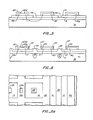
- FIGS 1 to 9 illustrate a portion of a DMOS transistor during various steps of a manufacturing process in accordance with the present invention.
- a process in accordance with the present invention begins with the step of forming a silicon dioxide layer 12 on a semiconductor substrate 10 ( Figure 1).
- water 10 consists of a layer of N type epitaxial silicon having a conductivity of about 1.5 ohm-centimeters and about 12 micrometers thick on a heavily N+ doped substrate.
- other semiconductors materials and materials having other conductivities and conductivity types are also appropriate.
- wafer includes substrate 10 and all layers formed directly or indirectly on substrate 10.
- Silicon dioxide layer 12 is typically thermally grown to a thickness of about 50 nanometers (nm). A silicon nitride layer 14 is then formed on silicon dioxide layer 12. Silicon nitride layer 14 is also typically about 50 nm thick and typically is formed by chemical vapor deposition. As will be discussed in greater detail below, silicon dioxide layer 12 and silicon nitride layer 14 serve as gate insulation for a subsequently formed DMOS transistor.
- a polycrystalline silicon layer 16 is then formed on silicon nitride layer 14.
- polycrystalline silicon layer 16 is formed to a thickness of about 500 nm by chemical vapor deposition.
- polycrystalline silicon layer 16 serves as the gate of the DMOS transistor.
- Polycrystalline silicon layer 16 is then doped to a sheet resistance of about 15 ohms per square with an N type dopant such as phosphorous.
- Polycrystalline silicon layer 16 is then covered with a photoresist layer 18 which is then patterned in a conventional manner, thereby exposing portions 16a to 16d of polycrystalline silicon layer 16. Exposed portions 16a to 16d of polycrystalline silicon layer 16 are then removed, thereby leaving polycrystalline silicon gates 16e and 16f and a field limiting ring 16g as illustrated in Figure 2.
- gates 16e and 16f and field limiting ring 16g are of a material other than polycrystalline silicon, e.g. a metal such as refractory metal or a silicide.
- Although polycrystalline silicon gates 16e and 16f appear as separate structures, in one embodiment they are a single contiguous polycrystalline silicon gate 17 joined outside the cross section of Figure 2.
- gates 16e and 16f are not a single contiguous region. However, in such an embodiment, gates 16e and 16f can be electrically connected together with a subsequently formed conductive layer.
- field limiting ring 16g surrounds the transistor and defines a subsequently formed EQR which surrounds ring 16g.
- photoresist layer 18 serves as a first mask for defining the gate of the DMOS transistor, a field limiting ring, and an EQR surrounding the transistor.
- silicon dioxide layer 20 is thermally grown to a thickness of about 500 nm.
- window region 22a defines an electrical contact to polycrystalline silicon gate 17 while window regions 22b and 22c define a P+ deep body region of the DMOS transistor.
- portion 20a of silicon dioxide layer 20 within window region 22a is removed and the portions of silicon nitride layer 14 within window regions 22b and 22c are removed.
- portion 20a is removed by placing the wafer in a buffered HF solution.
- photoresist layer 22 protects the underlying portions of silicon dioxide layer 20.
- the portion of silicon dioxide layer 20 within window region 22a is unprotected and therefore is removed by the HF solution.
- an oxidised nitride skin typically formed to a thickness of 5 to 10 nm during the preceding process steps within window regions 22b and 22c, is also removed by the HF solution.
- the wafer is removed from the buffered HF solution and placed, for example, in a phosphoric acid solution which removes the portions of silicon nitride layer 14 within window regions 22b and 22c, thereby forming window regions 14a and 14b.
- the wafer is then removed from the phosphoric acid solution and photoresist layer 22 is removed.
- the resulting structure is illustrated in Figure 5.
- etching instead of using an HF solution and phosphoric acid to etch silicon dioxide layer 20 and silicon nitride layer 14, respectively, plasma etching, reactive ion etching, or ion milling are used.
- P+ deep body regions 24 are formed in silicon substrate 10, e.g., by implanting P type ions in the portion of substrate 10 within window regions 14a and 14b.
- boron ions are implanted with a dosage of about 2 x 10¹⁴/cm2 and an implant energy of about 40 Kev. (Of importance, the implant energy and dose are selected to guarantee that ions are not implanted into the portions of the wafer covered by both silicon dioxide layer 12 and silicon nitride layer 14.)
- some ions are also implanted into polycrystalline silicon gate 17 where silicon dioxide layer 20 has been removed, because of the high N type dopant concentration in polycrystalline silicon gate 17, the gate conductivity is not significantly changed during this process.
- the portions of silicon dioxide layer 12 within window regions 14a and 14b prevent unwanted introduction of impurities into the semiconductor material within window regions 14a and 14b and prevent unwanted loss of boron during subsequent high temperature processing steps.
- a thin silicon dioxide layer 20b (typically about 50 nm thick) is formed on polycrystalline silicon 16e.
- portions 25 of silicon dioxide layer 12 above P+ deep body region 24 also increase in thickness.
- silicon dioxide layers 20b and 25 prevent impurities from diffusing out of gate 17 and into substrate 10.
- Figure 6a illustrates in plan view a portion of the transistor at this point in the manufacturing process. Region 24 is not shown in Figure 6a to simplify the illustration.
- the portions of silicon nitride layer 14 not covered by gate 17 or polycrystalline silicon ring 16g are then removed. In one embodiment this is done by placing the wafer in a phosphoric acid solution. However, the exposed portions of silicon nitride layer 14 can be removed in other ways as well, e.g., reactive ion etching or plasma etching. Silicon dioxide layer 20b and the exposed portions of silicon dioxide layer 12 are then removed by placing the wafer in a buffered HF solution. In other embodiments, layer 20b and the exposed portions of silicon dioxide layer 12 are removed with plasma etching or reactive ion etching.
- silicon dioxide layers 20 500 nm and 25 (220 to 230 nm)
- silicon dioxide layers 20 to 25 remain largely intact during this etching process.
- the portions of silicon nitride layer 14 and silicon dioxide layer 12 underneath gate 17 and polycrystalline silicon ring 16g also remain.
- only two photolithographic masks have been applied to the wafer.
- P type body region 26 is formed, e.g. by ion implantation.
- boron ions are implanted into substrate 10 with a dosage of about 5 x 10¹³/cm2 and an implant energy of approximately 50 Kev.
- the lateral extent of P type body region 26 is defined by edges 27 of gate 17. Therefore, no additional photolithographic masks or alignment steps are required during formation of body region 26.
- the wafer is then subjected to a drive-in process.
- a P type region 26a is formed concurrently with body region 26. However, as described below, P region 26a does not serve as a body region, but rather as part of an EQR.
- N+ source regions 28 are formed, e.g. by ion implantation.
- arsenic ions are implanted into substrate 10 with a dosage of about 5 x 10¹⁵/cm2 and an implant energy of about 40 Kev.
- the lateral extent of N+ source region 28 is also defined by edges 27 of gate 17 and the edge of silicon dioxide 25.
- the wafer is then subjected to another drive-in process. Thereafter, silicon dioxide 25 and any silicon dioxide formed above source regions 28 or within window 22a during the same drive-in process is removed in a blanket etching process, e.g. by placing the wafer in a buffered HF solution.
- N+ region 28a is formed concurrently with N+ source region 28. However, as described below, N+ region 28a does not serve as a source region but rather as part of the EQR.
- Conductive layer 30 is typically a metal layer such as aluminum or an alloy of aluminum. In other embodiments, conductive layer 30 is another metal. Conductive layer 30 serves as a source/body lead for the transistor as well as a gate lead.
- the wafer is then covered with a photoresist layer 32 which is patterned in a conventional manner, thereby exposing portions of conductive layer 30. The exposed portions of conductive layer 30 are then removed as illustrated in Figure 8.
- Photoresist layer 32 is then removed and the wafer is covered with a passivating layer of insulation such as plasma deposited silicon nitride layer 34.
- layer 34 is silicon dioxide.
- Portions of conductive layer 30 extend to an area of the wafer where bonding pads are formed (not shown).
- Passivating layer 34 is patterned by apply a fourth photolithographic mask to the wafer.
- the fourth photolithographic mask includes window regions exposing the portions of the passivating layer 34 above the bonding pads. The exposed portions of passivating layer 34 are then removed, thereby exposing the portions of conductive layer 30 at the bonding pad.
- a conductive layer 36 (also typically a metal such as aluminum) is formed on the bottom of the wafer ( Figure 9). Conductive layer 36 serves as a drain contact, and is typically not patterned.
- a portion 30a of conductive layer 30 (the EQR) is then shorted to substrate 10 and P region 26a. In one embodiment, this is accomplished by applying a high voltage to portion 30a of conductive layer 30 relative to substrate 10. Portion 30a is typically shorted to substrate 10 and P region 26a during wafer sort. (Wafer sort is the electrical testing of devices formed in the wafer before the wafer is cut into separate devices.) As mentioned above, the EQR is formed at the periphery of the transistor. As is known in the art, EQRs enhance reliability of a transistor. EQRs are described in "Surface Breakdown In Silicon Planar Diodes Equipped With Field Plate" by Conti et al., published in Solid State Electronics in 1972, Vol. 15.
- polycrystalline ring 16g serves as a field limiting ring. Ring 16g is typically electrically insulated from the other structures formed on the wafer. In an alternative embodiment, a plurality of polycrystalline silicon field limiting rings surround the transistor to further enhance transistor reliability.
- a process for manufacturing a DMOS transistor requiring only four photolithographic masks has been described in detail.
- the process is simple and minimizes the requirement of alignment tolerances.
- a transistor manufactured with the present process can be manufactured on a smaller surface area than prior art transistors.
- the gate to gate distance e.g. from polycrystalline silicon 16e to 16f
- this distance can be reduced to about 22 to 28 ⁇ m. This represents a savings of about 20% of the surface area of a transistor using a plurality of square cells.
- the above-described process is used to form an insulated gate bipolar transistor.
- source 28, body 26 and deep body region 24 are formed in an N type epitaxial layer which in turn is formed on a P+ substrate.
- the operation of insulated gate transistor is described in detail in "The Insulated Gate Transistor: A New Three-Terminal MOS-Controlled Bipolar Device," by Baliga et al., published in IEEE Transactions on Electron Devices, Vol. ED-31., No. 6, in June 1984.
- N and P channel transistors can be formed using this process.
- the transistor can be formed either in a substrate or in an epitaxial layer formed on a substrate. Accordingly, all such modifications come within the present invention.
Abstract
Description
- This invention relates to MOS transistors and more specifically to methods for manufacturing MOS transistors with a minimum number of masking steps. The invention also relates to double diffused MOS ("DMOS") transistors.
- A DMOS transistor is a MOS transistor having a channel length defined by the difference in diffusion of sequentially introduced impurities from a common edge or boundary. One example of a prior art process for manufacturing a DMOS transistor is discussed in U.S. Patent 4,443,931. It is known in the art that it is desirable to manufacture DMOS transistors while minimizing the number of masks used. One reason for this is that by minimizing the numbers of masks, the number of alignment steps is also minimized and therefore the need to accommodate alignment tolerances is minimized. As is known in the art, if the need to accommodate alignment tolerances is minimized, the size and cost of the resulting transistor is minimized.
- Another reason for minimizing the number of masking steps is that the complexity of the manufacturing process is correspondingly reduced and thus the cost of producing the transistor is also reduced.
- A method for manufacturing a DMOS transistor in accordance with the present invention includes the step of providing a gate insulation layer on a semiconductor substrate. The semiconductor substrate is typically N type silicon and the gate insulation layer typically comprises a silicon nitride layer formed on a silicon dioxide layer. A gate is then formed on the gate insulation layer. In one embodiment of the invention, the gate is polycrystalline silicon and is formed by depositing a polycrystalline silicon layer on the gate insulation layer and using a first photolithographic mask to protect portions of the polycrystalline silicon layer while the exposed portions of the polycrystalline silicon layer are removed.
- The resulting gate is covered with a second insulation layer which in one embodiment comprises silicon dioxide. A second photolithographic mask is formed on the wafer. In accordance with one novel feature of this invention, the second mask includes both a first window region defining the deep body region of the DMOS transistor and a second window region defining the gate contact. The portion of the second insulation layer within the second window region is removed. Of importance, the portion of the silicon nitride layer within the first window region is also removed and the underlying portion of the semiconductor substrate is thermally doped or implanted with P type dopant, thereby forming the deep body region.
- A silicon dioxide layer is then formed within the second window region, typically by thermal oxidation. Of importance, the thickness of the silicon dioxide within the first region also increases during this process. The exposed portion of the silicon nitride layer and the underlying silicon dioxide layer are then removed using a blanket etching process which does not require additional masking. At the conclusion of the blanket etching process, however, the silicon dioxide formed on the gate and the silicon dioxide formed above the deep body region remain. The silicon dioxide above the deep body region serves as an oxide mask which defines part of subsequently formed body and source regions.
- P type dopants are then implanted into the semiconductor substrate to form the body region of the DMOS transistor. Thereafter, N type dopants are implanted into the semiconductor substrate to form the source region. As mentioned above, the oxide mask grown over the deep body region prevents the underlying deep body region from being predoped or implanted with N type impurities. Of importance, the lateral extent of the source and body regions is defined by the edge of the gate and the oxide mask. Therefore, it is not necessary to use an extra masking step to define the source and body regions of the DMOS transistor.
- The oxide mask above the deep body region, the silicon dioxide within the second window, and any silicon dioxide formed above the source region during source and body drive-in are removed with a blanket etching process. A conductive layer (typically metal) is then formed on the surface of the wafer. A third photolithographic mask is applied to the wafer in order to pattern the conductive layer to form a gate lead and a source/body lead.
- The wafer is then coated with a passivation layer of material such as silicon nitride or silicon dioxide at a low temperature (typically less than 450°C). A fourth photolithographic mask is used to define regions where the passivation layer is to be removed, e.g. bonding pad regions. Of importance, the above described process requires only four photolithographic masks. Accordingly, the process is simpler than prior art DMOS manufacturing processes. Further, the need to increase the transistor size in order to allow for misalignment of the various photolithographic masks is reduced.
- In one embodiment, the transistor is laterally surrounded by an equipotential ring (EQR). In accordance with one novel feature of the invention, the EQR includes a P region (formed concurrently with the body region), an N+ region within the P region (formed concurrently with the source region) and a conductive ring formed on the N+ region (formed concurrently with the gate lead and the source/body lead). The conductive ring is electrically coupled to the substrate, the P region, and the N+ region, and is biased at the same voltage as the transistor drain. As is explained in greater detail below, the EQR enhances the reliability of the DMOS transistor. Of importance, the EQR is formed without any extra masking steps.
- Figures 1 to 9 illustrate a portion of a DMOS transistor during various steps of a manufacturing process in accordance with the present invention.
- A process in accordance with the present invention begins with the step of forming a
silicon dioxide layer 12 on a semiconductor substrate 10 (Figure 1). In one embodiment of the invention,water 10 consists of a layer of N type epitaxial silicon having a conductivity of about 1.5 ohm-centimeters and about 12 micrometers thick on a heavily N+ doped substrate. However, other semiconductors materials and materials having other conductivities and conductivity types are also appropriate. (As used herein, the term "wafer"" includessubstrate 10 and all layers formed directly or indirectly onsubstrate 10.) -
Silicon dioxide layer 12 is typically thermally grown to a thickness of about 50 nanometers (nm). Asilicon nitride layer 14 is then formed onsilicon dioxide layer 12.Silicon nitride layer 14 is also typically about 50 nm thick and typically is formed by chemical vapor deposition. As will be discussed in greater detail below,silicon dioxide layer 12 andsilicon nitride layer 14 serve as gate insulation for a subsequently formed DMOS transistor. - A
polycrystalline silicon layer 16 is then formed onsilicon nitride layer 14. In one embodiment,polycrystalline silicon layer 16 is formed to a thickness of about 500 nm by chemical vapor deposition. As described in greater detail below,polycrystalline silicon layer 16 serves as the gate of the DMOS transistor.Polycrystalline silicon layer 16 is then doped to a sheet resistance of about 15 ohms per square with an N type dopant such as phosphorous. -
Polycrystalline silicon layer 16 is then covered with aphotoresist layer 18 which is then patterned in a conventional manner, thereby exposingportions 16a to 16d ofpolycrystalline silicon layer 16. Exposedportions 16a to 16d ofpolycrystalline silicon layer 16 are then removed, thereby leavingpolycrystalline silicon gates field limiting ring 16g as illustrated in Figure 2. (In other embodiments,gates field limiting ring 16g are of a material other than polycrystalline silicon, e.g. a metal such as refractory metal or a silicide.) Althoughpolycrystalline silicon gates polycrystalline silicon gate 17 joined outside the cross section of Figure 2. (In another embodiment,gates gates field limiting ring 16g surrounds the transistor and defines a subsequently formed EQR which surroundsring 16g. In this way,photoresist layer 18 serves as a first mask for defining the gate of the DMOS transistor, a field limiting ring, and an EQR surrounding the transistor. - Referring to Figure 3, the remaining portions of
photoresist layer 18 are removed andpolycrystalline silicon gate 17 andring 16g are covered with asilicon dioxide layer 20. In one embodiment,silicon dioxide layer 20 is thermally grown to a thickness of about 500 nm. - The wafer is then covered with a
photoresist layer 22 which is then patterned in a known manner, thereby formingwindow regions photoresist layer 22. As will hereinafter become apparent,window region 22a defines an electrical contact topolycrystalline silicon gate 17 whilewindow regions - Referring to Figure 4, portion 20a of
silicon dioxide layer 20 withinwindow region 22a is removed and the portions ofsilicon nitride layer 14 withinwindow regions photoresist layer 22 protects the underlying portions ofsilicon dioxide layer 20. However, the portion ofsilicon dioxide layer 20 withinwindow region 22a is unprotected and therefore is removed by the HF solution. In addition, an oxidised nitride skin, typically formed to a thickness of 5 to 10 nm during the preceding process steps withinwindow regions silicon nitride layer 14 withinwindow regions window regions 14a and 14b. The wafer is then removed from the phosphoric acid solution andphotoresist layer 22 is removed. The resulting structure is illustrated in Figure 5. - In other embodiments of the invention, instead of using an HF solution and phosphoric acid to etch
silicon dioxide layer 20 andsilicon nitride layer 14, respectively, plasma etching, reactive ion etching, or ion milling are used. - Referring to Figure 6, P+
deep body regions 24 are formed insilicon substrate 10, e.g., by implanting P type ions in the portion ofsubstrate 10 withinwindow regions 14a and 14b. In one embodiment, boron ions are implanted with a dosage of about 2 x 10¹⁴/cm² and an implant energy of about 40 Kev. (Of importance, the implant energy and dose are selected to guarantee that ions are not implanted into the portions of the wafer covered by bothsilicon dioxide layer 12 andsilicon nitride layer 14.) Although during this process some ions are also implanted intopolycrystalline silicon gate 17 wheresilicon dioxide layer 20 has been removed, because of the high N type dopant concentration inpolycrystalline silicon gate 17, the gate conductivity is not significantly changed during this process. It is also noted that the portions ofsilicon dioxide layer 12 withinwindow regions 14a and 14b prevent unwanted introduction of impurities into the semiconductor material withinwindow regions 14a and 14b and prevent unwanted loss of boron during subsequent high temperature processing steps. - The wafer is then subjected to a drive-in process. During this drive-in process, a thin
silicon dioxide layer 20b (typically about 50 nm thick) is formed onpolycrystalline silicon 16e. In addition,portions 25 ofsilicon dioxide layer 12 above P+deep body region 24 also increase in thickness. Of importance, during the diffusion ofP+ regions 24, silicon dioxide layers 20b and 25 prevent impurities from diffusing out ofgate 17 and intosubstrate 10. - Figure 6a illustrates in plan view a portion of the transistor at this point in the manufacturing process.
Region 24 is not shown in Figure 6a to simplify the illustration. - The portions of
silicon nitride layer 14 not covered bygate 17 orpolycrystalline silicon ring 16g are then removed. In one embodiment this is done by placing the wafer in a phosphoric acid solution. However, the exposed portions ofsilicon nitride layer 14 can be removed in other ways as well, e.g., reactive ion etching or plasma etching.Silicon dioxide layer 20b and the exposed portions ofsilicon dioxide layer 12 are then removed by placing the wafer in a buffered HF solution. In other embodiments,layer 20b and the exposed portions ofsilicon dioxide layer 12 are removed with plasma etching or reactive ion etching. Of importance because of the thickness of silicon dioxide layers 20 (500 nm) and 25 (220 to 230 nm), silicon dioxide layers 20 to 25 remain largely intact during this etching process. In addition, the portions ofsilicon nitride layer 14 andsilicon dioxide layer 12 underneathgate 17 andpolycrystalline silicon ring 16g also remain. Of importance, up to this point in the process, only two photolithographic masks have been applied to the wafer. - Referring to Figure 7, P
type body region 26 is formed, e.g. by ion implantation. In one embodiment, boron ions are implanted intosubstrate 10 with a dosage of about 5 x 10¹³/cm² and an implant energy of approximately 50 Kev. Of importance, the lateral extent of Ptype body region 26 is defined byedges 27 ofgate 17. Therefore, no additional photolithographic masks or alignment steps are required during formation ofbody region 26. The wafer is then subjected to a drive-in process. -
A P type region 26a is formed concurrently withbody region 26. However, as described below,P region 26a does not serve as a body region, but rather as part of an EQR. - Thereafter,
N+ source regions 28 are formed, e.g. by ion implantation. In one embodiment, arsenic ions are implanted intosubstrate 10 with a dosage of about 5 x 10¹⁵/cm² and an implant energy of about 40 Kev. The lateral extent ofN+ source region 28 is also defined byedges 27 ofgate 17 and the edge ofsilicon dioxide 25. The wafer is then subjected to another drive-in process. Thereafter,silicon dioxide 25 and any silicon dioxide formed abovesource regions 28 or withinwindow 22a during the same drive-in process is removed in a blanket etching process, e.g. by placing the wafer in a buffered HF solution. - An
N+ region 28a is formed concurrently withN+ source region 28. However, as described below,N+ region 28a does not serve as a source region but rather as part of the EQR. - Referring to Figure 8, the wafer is covered with a
conductive layer 30.Conductive layer 30 is typically a metal layer such as aluminum or an alloy of aluminum. In other embodiments,conductive layer 30 is another metal.Conductive layer 30 serves as a source/body lead for the transistor as well as a gate lead. The wafer is then covered with aphotoresist layer 32 which is patterned in a conventional manner, thereby exposing portions ofconductive layer 30. The exposed portions ofconductive layer 30 are then removed as illustrated in Figure 8. -
Photoresist layer 32 is then removed and the wafer is covered with a passivating layer of insulation such as plasma depositedsilicon nitride layer 34. In other embodiments,layer 34 is silicon dioxide. Portions ofconductive layer 30 extend to an area of the wafer where bonding pads are formed (not shown).Passivating layer 34 is patterned by apply a fourth photolithographic mask to the wafer. The fourth photolithographic mask includes window regions exposing the portions of thepassivating layer 34 above the bonding pads. The exposed portions ofpassivating layer 34 are then removed, thereby exposing the portions ofconductive layer 30 at the bonding pad. - After
passivation layer 34 is patterned, a conductive layer 36 (also typically a metal such as aluminum) is formed on the bottom of the wafer (Figure 9).Conductive layer 36 serves as a drain contact, and is typically not patterned. - A portion 30a of conductive layer 30 (the EQR) is then shorted to
substrate 10 andP region 26a. In one embodiment, this is accomplished by applying a high voltage to portion 30a ofconductive layer 30 relative tosubstrate 10. Portion 30a is typically shorted tosubstrate 10 andP region 26a during wafer sort. (Wafer sort is the electrical testing of devices formed in the wafer before the wafer is cut into separate devices.) As mentioned above, the EQR is formed at the periphery of the transistor. As is known in the art, EQRs enhance reliability of a transistor. EQRs are described in "Surface Breakdown In Silicon Planar Diodes Equipped With Field Plate" by Conti et al., published in Solid State Electronics in 1972, Vol. 15. - As mentioned above,
polycrystalline ring 16g serves as a field limiting ring.Ring 16g is typically electrically insulated from the other structures formed on the wafer. In an alternative embodiment, a plurality of polycrystalline silicon field limiting rings surround the transistor to further enhance transistor reliability. - It will be appreciated that a process for manufacturing a DMOS transistor requiring only four photolithographic masks has been described in detail. The process is simple and minimizes the requirement of alignment tolerances. Accordingly, a transistor manufactured with the present process can be manufactured on a smaller surface area than prior art transistors. For example, in a typical prior art transistor, the gate to gate distance (e.g. from
polycrystalline silicon 16e to 16f) is about 25 to 30 µm. By using the process of the present invention, this distance can be reduced to about 22 to 28 µm. This represents a savings of about 20% of the surface area of a transistor using a plurality of square cells. - In an alternative embodiment, the above-described process is used to form an insulated gate bipolar transistor. In such an embodiment,
source 28,body 26 anddeep body region 24 are formed in an N type epitaxial layer which in turn is formed on a P+ substrate. The operation of insulated gate transistor is described in detail in "The Insulated Gate Transistor: A New Three-Terminal MOS-Controlled Bipolar Device," by Baliga et al., published in IEEE Transactions on Electron Devices, Vol. ED-31., No. 6, in June 1984. - While the invention has been described with reference to specific details, those skilled in the art will recognise that changes can be made in form and detail without departing from the spirit and scope of the invention. For example, both N and P channel transistors can be formed using this process. In addition, the transistor can be formed either in a substrate or in an epitaxial layer formed on a substrate. Accordingly, all such modifications come within the present invention.
Claims (19)
forming an electrically conductive layer on the surface of said second and fourth semiconductor regions and said gate, a first portion of said electrically conductive layer electrically contacting said gate, a second portion of said electrically conductive layer electrically contacting said second and fourth semiconductor regions, a third portion of said electrically conductive layer serving as bonding pads;
forming a passivating insulation layer on said electrically conductive layer; and
etching said passivating insulation layer, thereby exposing said bonding pads, whereby said process uses only four photolithographic masks.
forming first, second and third electrically conductive layers, said first electrically conductive layer electrically contacting said gate, said second electrically conductive layer electrically contacting said second and fourth semiconductor regions, said EQR comprising said third electrically conductive layer.
a fifth semiconductor region of said second conductivity type formed in said first semiconductor region; and
a sixth semiconductor region of said first conductivity type formed in said fifth semiconductor region, said third electrically conductive layer being formed above and electrically contacting said sixth semiconductor region, said third electrically conductive layer also electrically contacting said fifth and first semiconductor regions.
removing the portions of said silicon nitride layer not covered by said gate with a first blanket etching process after said step of forming said second semiconductor region;
removing said masking layer and the portion of said silicon dioxide layer not covered by said gate with a second blanket etching process after forming said fourth semiconductor region, thereby exposing portions of said second and fourth semiconductor regions; and
forming electrically conductive material on said exposed portions of said second and fourth semiconductor regions.
a second semiconductor region of a second conductivity type formed in said first semiconductor region;
a third semiconductor region of said first conductivity type formed within said second semiconductor region; and
a first conductive layer formed on and electrically contacting said third semiconductor region, said first conductive layer also electrically contacting said second and first semiconductor regions.
Applications Claiming Priority (2)
| Application Number | Priority Date | Filing Date | Title |
|---|---|---|---|
| US838217 | 1986-03-10 | ||
| US06/838,217 US4798810A (en) | 1986-03-10 | 1986-03-10 | Method for manufacturing a power MOS transistor |
Publications (2)
| Publication Number | Publication Date |
|---|---|
| EP0241059A2 true EP0241059A2 (en) | 1987-10-14 |
| EP0241059A3 EP0241059A3 (en) | 1988-08-24 |
Family
ID=25276564
Family Applications (1)
| Application Number | Title | Priority Date | Filing Date |
|---|---|---|---|
| EP87200388A Withdrawn EP0241059A3 (en) | 1986-03-10 | 1987-03-03 | Method for manufacturing a power mos transistor |
Country Status (3)
| Country | Link |
|---|---|
| US (1) | US4798810A (en) |
| EP (1) | EP0241059A3 (en) |
| JP (1) | JPS62213167A (en) |
Cited By (2)
| Publication number | Priority date | Publication date | Assignee | Title |
|---|---|---|---|---|
| EP0460251A1 (en) * | 1990-06-05 | 1991-12-11 | Siemens Aktiengesellschaft | Method of fabricating a power-MISFET |
| EP0543257A2 (en) * | 1991-11-13 | 1993-05-26 | Siemens Aktiengesellschaft | Method of manufacturing a power-MISFET |
Families Citing this family (25)
| Publication number | Priority date | Publication date | Assignee | Title |
|---|---|---|---|---|
| US4853345A (en) * | 1988-08-22 | 1989-08-01 | Delco Electronics Corporation | Process for manufacture of a vertical DMOS transistor |
| JPH02281662A (en) * | 1989-04-21 | 1990-11-19 | Mitsubishi Electric Corp | Semiconductor device |
| IT1236994B (en) * | 1989-12-29 | 1993-05-12 | Sgs Thomson Microelectronics | PROCESS FOR THE MANUFACTURE OF POWER MOS SEMICONDUCTIVE DEVICES AND DEVICES OBTAINED WITH IT |
| KR940011483B1 (en) * | 1990-11-28 | 1994-12-19 | 가부시끼가이샤 도시바 | Semiconductor device with nitrided gate insulating film |
| US5288653A (en) * | 1991-02-27 | 1994-02-22 | Nec Corporation | Process of fabricating an insulated-gate field effect transistor |
| US5182222A (en) * | 1991-06-26 | 1993-01-26 | Texas Instruments Incorporated | Process for manufacturing a DMOS transistor |
| IT1250233B (en) * | 1991-11-29 | 1995-04-03 | St Microelectronics Srl | PROCEDURE FOR THE MANUFACTURE OF INTEGRATED CIRCUITS IN MOS TECHNOLOGY. |
| US5346835A (en) * | 1992-07-06 | 1994-09-13 | Texas Instruments Incorporated | Triple diffused lateral resurf insulated gate field effect transistor compatible with process and method |
| US5369045A (en) * | 1993-07-01 | 1994-11-29 | Texas Instruments Incorporated | Method for forming a self-aligned lateral DMOS transistor |
| US5414283A (en) * | 1993-11-19 | 1995-05-09 | Ois Optical Imaging Systems, Inc. | TFT with reduced parasitic capacitance |
| EP0661735B1 (en) * | 1993-12-29 | 2001-03-07 | Consorzio per la Ricerca sulla Microelettronica nel Mezzogiorno | Process for the manufacturing of integrated circuits, particularly of intelligent power semiconductor devices |
| JP3275536B2 (en) | 1994-05-31 | 2002-04-15 | 三菱電機株式会社 | Semiconductor device and manufacturing method thereof |
| US5817546A (en) * | 1994-06-23 | 1998-10-06 | Stmicroelectronics S.R.L. | Process of making a MOS-technology power device |
| EP0689238B1 (en) * | 1994-06-23 | 2002-02-20 | STMicroelectronics S.r.l. | MOS-technology power device manufacturing process |
| US5545915A (en) * | 1995-01-23 | 1996-08-13 | Delco Electronics Corporation | Semiconductor device having field limiting ring and a process therefor |
| US5798554A (en) * | 1995-02-24 | 1998-08-25 | Consorzio Per La Ricerca Sulla Microelettronica Nel Mezzogiorno | MOS-technology power device integrated structure and manufacturing process thereof |
| EP0772242B1 (en) | 1995-10-30 | 2006-04-05 | STMicroelectronics S.r.l. | Single feature size MOS technology power device |
| EP0772241B1 (en) * | 1995-10-30 | 2004-06-09 | STMicroelectronics S.r.l. | High density MOS technology power device |
| US6228719B1 (en) | 1995-11-06 | 2001-05-08 | Stmicroelectronics S.R.L. | MOS technology power device with low output resistance and low capacitance, and related manufacturing process |
| US5631484A (en) * | 1995-12-26 | 1997-05-20 | Motorola, Inc. | Method of manufacturing a semiconductor device and termination structure |
| EP0782201B1 (en) * | 1995-12-28 | 2000-08-30 | STMicroelectronics S.r.l. | MOS-technology power device integrated structure |
| US5602046A (en) * | 1996-04-12 | 1997-02-11 | National Semiconductor Corporation | Integrated zener diode protection structures and fabrication methods for DMOS power devices |
| JP3464382B2 (en) * | 1998-05-18 | 2003-11-10 | ローム株式会社 | Manufacturing method of vertical double diffusion MOSFET |
| DE69839439D1 (en) | 1998-05-26 | 2008-06-19 | St Microelectronics Srl | MOS technology power arrangement with high integration density |
| US7932536B2 (en) * | 2007-03-09 | 2011-04-26 | Diodes Incorporated | Power rectifiers and method of making same |
Citations (4)
| Publication number | Priority date | Publication date | Assignee | Title |
|---|---|---|---|---|
| GB2082385A (en) * | 1980-08-18 | 1982-03-03 | Int Rectifier Corp | Process for manufacture of high power mosfet with laterally distributed high carrier density beneath the gate oxide |
| WO1982002981A1 (en) * | 1981-02-23 | 1982-09-02 | Inc Motorola | Mos power transistor |
| US4466176A (en) * | 1982-08-09 | 1984-08-21 | General Electric Company | Process for manufacturing insulated-gate semiconductor devices with integral shorts |
| EP0118921A2 (en) * | 1983-03-14 | 1984-09-19 | Nissan Motor Co., Ltd. | MOSFET with high density of integration and low on resistance |
Family Cites Families (16)
| Publication number | Priority date | Publication date | Assignee | Title |
|---|---|---|---|---|
| US3909119A (en) * | 1974-02-06 | 1975-09-30 | Westinghouse Electric Corp | Guarded planar PN junction semiconductor device |
| US4158206A (en) * | 1977-02-07 | 1979-06-12 | Rca Corporation | Semiconductor device |
| US4374389A (en) * | 1978-06-06 | 1983-02-15 | General Electric Company | High breakdown voltage semiconductor device |
| US4345265A (en) * | 1980-04-14 | 1982-08-17 | Supertex, Inc. | MOS Power transistor with improved high-voltage capability |
| US4300150A (en) * | 1980-06-16 | 1981-11-10 | North American Philips Corporation | Lateral double-diffused MOS transistor device |
| US4414560A (en) * | 1980-11-17 | 1983-11-08 | International Rectifier Corporation | Floating guard region and process of manufacture for semiconductor reverse conducting switching device using spaced MOS transistors having a common drain region |
| JPS5793573A (en) * | 1980-12-03 | 1982-06-10 | Hitachi Ltd | Mis semiconductor device |
| JPS57160159A (en) * | 1981-03-28 | 1982-10-02 | Toshiba Corp | High breakdown voltage planar type semiconductor device |
| US4468686A (en) * | 1981-11-13 | 1984-08-28 | Intersil, Inc. | Field terminating structure |
| JPS5887874A (en) * | 1981-11-20 | 1983-05-25 | Hitachi Ltd | Insulated gate type semiconductor device |
| US4443931A (en) * | 1982-06-28 | 1984-04-24 | General Electric Company | Method of fabricating a semiconductor device with a base region having a deep portion |
| US4789882A (en) * | 1983-03-21 | 1988-12-06 | International Rectifier Corporation | High power MOSFET with direct connection from connection pads to underlying silicon |
| JPS5925264A (en) * | 1983-06-15 | 1984-02-09 | Hitachi Ltd | Mis integrated circuit device |
| US4631564A (en) * | 1984-10-23 | 1986-12-23 | Rca Corporation | Gate shield structure for power MOS device |
| US4646117A (en) * | 1984-12-05 | 1987-02-24 | General Electric Company | Power semiconductor devices with increased turn-off current ratings and limited current density in peripheral portions |
| US4609929A (en) * | 1984-12-21 | 1986-09-02 | North American Philips Corporation | Conductivity-enhanced combined lateral MOS/bipolar transistor |
-
1986
- 1986-03-10 US US06/838,217 patent/US4798810A/en not_active Expired - Lifetime
-
1987
- 1987-03-03 EP EP87200388A patent/EP0241059A3/en not_active Withdrawn
- 1987-03-10 JP JP62053236A patent/JPS62213167A/en active Pending
Patent Citations (4)
| Publication number | Priority date | Publication date | Assignee | Title |
|---|---|---|---|---|
| GB2082385A (en) * | 1980-08-18 | 1982-03-03 | Int Rectifier Corp | Process for manufacture of high power mosfet with laterally distributed high carrier density beneath the gate oxide |
| WO1982002981A1 (en) * | 1981-02-23 | 1982-09-02 | Inc Motorola | Mos power transistor |
| US4466176A (en) * | 1982-08-09 | 1984-08-21 | General Electric Company | Process for manufacturing insulated-gate semiconductor devices with integral shorts |
| EP0118921A2 (en) * | 1983-03-14 | 1984-09-19 | Nissan Motor Co., Ltd. | MOSFET with high density of integration and low on resistance |
Cited By (4)
| Publication number | Priority date | Publication date | Assignee | Title |
|---|---|---|---|---|
| EP0460251A1 (en) * | 1990-06-05 | 1991-12-11 | Siemens Aktiengesellschaft | Method of fabricating a power-MISFET |
| US5087577A (en) * | 1990-06-05 | 1992-02-11 | Siemens Aktiengesellschaft | Manufacturing method for a power misfet |
| EP0543257A2 (en) * | 1991-11-13 | 1993-05-26 | Siemens Aktiengesellschaft | Method of manufacturing a power-MISFET |
| EP0543257A3 (en) * | 1991-11-13 | 1994-07-13 | Siemens Ag | Method of manufacturing a power-misfet |
Also Published As
| Publication number | Publication date |
|---|---|
| EP0241059A3 (en) | 1988-08-24 |
| US4798810A (en) | 1989-01-17 |
| JPS62213167A (en) | 1987-09-19 |
Similar Documents
| Publication | Publication Date | Title |
|---|---|---|
| US4798810A (en) | Method for manufacturing a power MOS transistor | |
| EP0635888B1 (en) | Structure and fabrication of power MOSFETs, including termination structure | |
| US4149307A (en) | Process for fabricating insulated-gate field-effect transistors with self-aligned contacts | |
| US4757032A (en) | Method for DMOS semiconductor device fabrication | |
| EP0094891B1 (en) | Method of fabricating a vertical power mosfet structure | |
| US5731604A (en) | Semiconductor device MOS gated | |
| US4417385A (en) | Processes for manufacturing insulated-gate semiconductor devices with integral shorts | |
| US5783474A (en) | Reduced mask process for manufacture of MOS gated devices using dopant-enhanced-oxidation of semiconductor | |
| US4752589A (en) | Process for the production of bipolar transistors and complementary MOS transistors on a common silicon substrate | |
| EP0583023A1 (en) | Trenched DMOS transistor fabrication using six masks | |
| US5786619A (en) | Depletion mode power MOSFET with refractory gate and method of making same | |
| US4258465A (en) | Method for fabrication of offset gate MIS device | |
| EP0918353A1 (en) | A method of manufacturing a recessed insulated gate field-effect semiconductor device | |
| JPH08264787A (en) | Edge termination method of power mosfet and its structure | |
| GB2318685A (en) | MOS gated device with self aligned cells | |
| EP0654829A1 (en) | Increased density MOS-gated double diffused semiconductor devices | |
| US4816882A (en) | Power MOS transistor with equipotential ring | |
| US4637128A (en) | Method of producing semiconductor device | |
| US4878100A (en) | Triple-implanted drain in transistor made by oxide sidewall-spacer method | |
| EP0073697B1 (en) | Method of forming a metal semiconductor field effect transistor | |
| US5879968A (en) | Process for manufacture of a P-channel MOS gated device with base implant through the contact window | |
| US4786610A (en) | Method of making a monolithic integrated circuit comprising at least one bipolar planar transistor | |
| US4464825A (en) | Process for fabrication of high-speed radiation hard bipolar semiconductor devices | |
| EP0242893B1 (en) | Method of manufacturing a semiconductor device | |
| US5595918A (en) | Process for manufacture of P channel MOS-gated device |
Legal Events
| Date | Code | Title | Description |
|---|---|---|---|
| PUAI | Public reference made under article 153(3) epc to a published international application that has entered the european phase |
Free format text: ORIGINAL CODE: 0009012 |
|
| AK | Designated contracting states |
Kind code of ref document: A2 Designated state(s): BE DE FR GB IT NL |
|
| PUAL | Search report despatched |
Free format text: ORIGINAL CODE: 0009013 |
|
| AK | Designated contracting states |
Kind code of ref document: A3 Designated state(s): BE DE FR GB IT NL |
|
| STAA | Information on the status of an ep patent application or granted ep patent |
Free format text: STATUS: THE APPLICATION IS DEEMED TO BE WITHDRAWN |
|
| 18D | Application deemed to be withdrawn |
Effective date: 19890227 |
|
| RIN1 | Information on inventor provided before grant (corrected) |
Inventor name: BLANCHARD, RICHARD A. Inventor name: COGAN, ADRIAN I. |