EP0240683A1 - Fabrication of insulated gallium arsenide-gate FET with self-aligned source/drain and submicron channel length - Google Patents
Fabrication of insulated gallium arsenide-gate FET with self-aligned source/drain and submicron channel length Download PDFInfo
- Publication number
- EP0240683A1 EP0240683A1 EP87102621A EP87102621A EP0240683A1 EP 0240683 A1 EP0240683 A1 EP 0240683A1 EP 87102621 A EP87102621 A EP 87102621A EP 87102621 A EP87102621 A EP 87102621A EP 0240683 A1 EP0240683 A1 EP 0240683A1
- Authority
- EP
- European Patent Office
- Prior art keywords
- layer
- gate
- gaas
- submicron
- conductive
- Prior art date
- Legal status (The legal status is an assumption and is not a legal conclusion. Google has not performed a legal analysis and makes no representation as to the accuracy of the status listed.)
- Granted
Links
- 238000004519 manufacturing process Methods 0.000 title description 5
- GYHNNYVSQQEPJS-UHFFFAOYSA-N Gallium Chemical compound [Ga] GYHNNYVSQQEPJS-UHFFFAOYSA-N 0.000 title 1
- 229910052733 gallium Inorganic materials 0.000 title 1
- 229910001218 Gallium arsenide Inorganic materials 0.000 claims abstract description 75
- 238000000034 method Methods 0.000 claims abstract description 50
- 230000008569 process Effects 0.000 claims abstract description 28
- 239000012212 insulator Substances 0.000 claims abstract description 26
- 229920002120 photoresistant polymer Polymers 0.000 claims abstract description 21
- 239000000758 substrate Substances 0.000 claims abstract description 21
- 238000005468 ion implantation Methods 0.000 claims abstract description 12
- 230000005669 field effect Effects 0.000 claims abstract description 7
- 229910000980 Aluminium gallium arsenide Inorganic materials 0.000 claims abstract 10
- 238000005530 etching Methods 0.000 claims description 22
- 229910020776 SixNy Inorganic materials 0.000 claims description 14
- 239000000463 material Substances 0.000 claims description 14
- 238000000137 annealing Methods 0.000 claims description 10
- VYPSYNLAJGMNEJ-UHFFFAOYSA-N Silicium dioxide Chemical group O=[Si]=O VYPSYNLAJGMNEJ-UHFFFAOYSA-N 0.000 claims description 8
- 239000011368 organic material Substances 0.000 claims description 7
- XUIMIQQOPSSXEZ-UHFFFAOYSA-N Silicon Chemical compound [Si] XUIMIQQOPSSXEZ-UHFFFAOYSA-N 0.000 claims description 6
- 238000000151 deposition Methods 0.000 claims description 6
- 239000003870 refractory metal Substances 0.000 claims description 6
- 229910052710 silicon Inorganic materials 0.000 claims description 6
- 239000010703 silicon Substances 0.000 claims description 6
- 239000004642 Polyimide Substances 0.000 claims description 5
- 150000002500 ions Chemical class 0.000 claims description 5
- 229920001721 polyimide Polymers 0.000 claims description 5
- 239000004065 semiconductor Substances 0.000 claims description 5
- 229910052814 silicon oxide Inorganic materials 0.000 claims description 4
- 238000000206 photolithography Methods 0.000 claims description 3
- MBGCACIOPCILDG-UHFFFAOYSA-N [Ni].[Ge].[Au] Chemical compound [Ni].[Ge].[Au] MBGCACIOPCILDG-UHFFFAOYSA-N 0.000 claims description 2
- 239000011248 coating agent Substances 0.000 claims description 2
- 238000000576 coating method Methods 0.000 claims description 2
- 229910052736 halogen Inorganic materials 0.000 claims description 2
- 150000002367 halogens Chemical class 0.000 claims description 2
- 238000002513 implantation Methods 0.000 claims description 2
- 239000010410 layer Substances 0.000 claims 69
- 239000004020 conductor Substances 0.000 claims 11
- 239000012044 organic layer Substances 0.000 claims 3
- 229910001092 metal group alloy Inorganic materials 0.000 claims 2
- 238000001020 plasma etching Methods 0.000 claims 2
- 229910000990 Ni alloy Inorganic materials 0.000 claims 1
- QVGXLLKOCUKJST-UHFFFAOYSA-N atomic oxygen Chemical compound [O] QVGXLLKOCUKJST-UHFFFAOYSA-N 0.000 claims 1
- 229910052760 oxygen Inorganic materials 0.000 claims 1
- 239000001301 oxygen Substances 0.000 claims 1
- 238000000059 patterning Methods 0.000 claims 1
- 230000001131 transforming effect Effects 0.000 claims 1
- 229910052751 metal Inorganic materials 0.000 abstract description 38
- 239000002184 metal Substances 0.000 abstract description 38
- 238000001465 metallisation Methods 0.000 abstract description 2
- JBRZTFJDHDCESZ-UHFFFAOYSA-N AsGa Chemical compound [As]#[Ga] JBRZTFJDHDCESZ-UHFFFAOYSA-N 0.000 description 50
- 239000002019 doping agent Substances 0.000 description 5
- 229910052782 aluminium Inorganic materials 0.000 description 4
- XAGFODPZIPBFFR-UHFFFAOYSA-N aluminium Chemical group [Al] XAGFODPZIPBFFR-UHFFFAOYSA-N 0.000 description 4
- 239000002131 composite material Substances 0.000 description 4
- 239000007789 gas Substances 0.000 description 4
- 238000002955 isolation Methods 0.000 description 4
- 125000006850 spacer group Chemical group 0.000 description 3
- QGZKDVFQNNGYKY-UHFFFAOYSA-N Ammonia Chemical compound N QGZKDVFQNNGYKY-UHFFFAOYSA-N 0.000 description 2
- ZOKXTWBITQBERF-UHFFFAOYSA-N Molybdenum Chemical compound [Mo] ZOKXTWBITQBERF-UHFFFAOYSA-N 0.000 description 2
- 230000008901 benefit Effects 0.000 description 2
- 230000008020 evaporation Effects 0.000 description 2
- 238000001704 evaporation Methods 0.000 description 2
- 239000007943 implant Substances 0.000 description 2
- 230000010354 integration Effects 0.000 description 2
- 238000001459 lithography Methods 0.000 description 2
- 238000005272 metallurgy Methods 0.000 description 2
- 239000000203 mixture Substances 0.000 description 2
- 238000012986 modification Methods 0.000 description 2
- 230000004048 modification Effects 0.000 description 2
- 229910052750 molybdenum Inorganic materials 0.000 description 2
- 239000011733 molybdenum Substances 0.000 description 2
- 230000003071 parasitic effect Effects 0.000 description 2
- 238000002161 passivation Methods 0.000 description 2
- 235000012239 silicon dioxide Nutrition 0.000 description 2
- 239000000377 silicon dioxide Substances 0.000 description 2
- 238000004528 spin coating Methods 0.000 description 2
- BLRPTPMANUNPDV-UHFFFAOYSA-N Silane Chemical compound [SiH4] BLRPTPMANUNPDV-UHFFFAOYSA-N 0.000 description 1
- MDPILPRLPQYEEN-UHFFFAOYSA-N aluminium arsenide Chemical compound [As]#[Al] MDPILPRLPQYEEN-UHFFFAOYSA-N 0.000 description 1
- 229910021529 ammonia Inorganic materials 0.000 description 1
- RBFQJDQYXXHULB-UHFFFAOYSA-N arsane Chemical compound [AsH3] RBFQJDQYXXHULB-UHFFFAOYSA-N 0.000 description 1
- 238000004380 ashing Methods 0.000 description 1
- 229910052796 boron Inorganic materials 0.000 description 1
- -1 boron ions Chemical class 0.000 description 1
- 230000015556 catabolic process Effects 0.000 description 1
- 239000002800 charge carrier Substances 0.000 description 1
- 238000005229 chemical vapour deposition Methods 0.000 description 1
- 230000007812 deficiency Effects 0.000 description 1
- 238000006731 degradation reaction Methods 0.000 description 1
- 230000008021 deposition Effects 0.000 description 1
- 238000010586 diagram Methods 0.000 description 1
- PXBRQCKWGAHEHS-UHFFFAOYSA-N dichlorodifluoromethane Chemical compound FC(F)(Cl)Cl PXBRQCKWGAHEHS-UHFFFAOYSA-N 0.000 description 1
- 235000019404 dichlorodifluoromethane Nutrition 0.000 description 1
- 239000003989 dielectric material Substances 0.000 description 1
- 238000000609 electron-beam lithography Methods 0.000 description 1
- 238000005516 engineering process Methods 0.000 description 1
- 230000006870 function Effects 0.000 description 1
- QOSMEWGVERQLHJ-UHFFFAOYSA-N germanium molybdenum Chemical compound [Ge].[Mo] QOSMEWGVERQLHJ-UHFFFAOYSA-N 0.000 description 1
- 239000001307 helium Substances 0.000 description 1
- 229910052734 helium Inorganic materials 0.000 description 1
- SWQJXJOGLNCZEY-UHFFFAOYSA-N helium atom Chemical compound [He] SWQJXJOGLNCZEY-UHFFFAOYSA-N 0.000 description 1
- 230000006872 improvement Effects 0.000 description 1
- 239000012535 impurity Substances 0.000 description 1
- 238000007737 ion beam deposition Methods 0.000 description 1
- 238000005224 laser annealing Methods 0.000 description 1
- 230000000873 masking effect Effects 0.000 description 1
- 150000002739 metals Chemical class 0.000 description 1
- 238000001451 molecular beam epitaxy Methods 0.000 description 1
- 238000005457 optimization Methods 0.000 description 1
- 238000000623 plasma-assisted chemical vapour deposition Methods 0.000 description 1
- 230000002250 progressing effect Effects 0.000 description 1
- 230000035945 sensitivity Effects 0.000 description 1
- 229910000077 silane Inorganic materials 0.000 description 1
- 238000005507 spraying Methods 0.000 description 1
- 238000004544 sputter deposition Methods 0.000 description 1
- 230000005533 two-dimensional electron gas Effects 0.000 description 1
Images

Classifications
-
- H—ELECTRICITY
- H01—ELECTRIC ELEMENTS
- H01L—SEMICONDUCTOR DEVICES NOT COVERED BY CLASS H10
- H01L29/00—Semiconductor devices adapted for rectifying, amplifying, oscillating or switching, or capacitors or resistors with at least one potential-jump barrier or surface barrier, e.g. PN junction depletion layer or carrier concentration layer; Details of semiconductor bodies or of electrodes thereof ; Multistep manufacturing processes therefor
- H01L29/66—Types of semiconductor device ; Multistep manufacturing processes therefor
- H01L29/66007—Multistep manufacturing processes
- H01L29/66075—Multistep manufacturing processes of devices having semiconductor bodies comprising group 14 or group 13/15 materials
- H01L29/66227—Multistep manufacturing processes of devices having semiconductor bodies comprising group 14 or group 13/15 materials the devices being controllable only by the electric current supplied or the electric potential applied, to an electrode which does not carry the current to be rectified, amplified or switched, e.g. three-terminal devices
- H01L29/66409—Unipolar field-effect transistors
- H01L29/66893—Unipolar field-effect transistors with a PN junction gate, i.e. JFET
- H01L29/66924—Unipolar field-effect transistors with a PN junction gate, i.e. JFET with an active layer made of a group 13/15 material
Definitions
- the invention relates to gallium arsenide (GaAs) integrated circuit fabrication technology, and more particularly, to a method of forming on a GaAs substrate an insulated GaAs-gate field effect transistor (FET) having self-aligned source/drain and submicron channel length.
- GaAs gallium arsenide
- FET field effect transistor
- MOSFET metal-semiconductor field effect transistor
- D MESFET depletion mode MESFET
- E-MESFET enhancement mode MESFET
- the basic MESFET consists of a metal Schottky gate placed between a source and a drain region. The transistor typically is formed in two ionimplantation steps: a relatively low concentration implant below the gate region provides the channel, and a relatively high concentration implant in close vicinity to the gate provides the source and the drain regions.
- a D-MESFET In a D-MESFET, with no voltage applied to the gate, current flows through the channel between the transistor's source and drain when a voltage is applied across the source and drain. The application of a gate voltage (negative with respect to the source) causes the channel to become narrower, reducing current flow. If a sufficiently negative gate voltage is applied, the current flow is pinched off. In an E-MESFET, the region under the gate is doped such that the channel is pinched off when no gate voltage is applied. A small positive gate voltage with respect to the source will initiate current flow.
- HEMT high electron mobility transistor
- SDHT selectively doped heterojunction transistor
- MODFET modulation doped FET
- TEGFET two-dimensional electron gas FET
- the device described in this article consists of a pair of undoped GaAs layers sandwiching a layer of silicon doped GaAlAs.
- a Schottky gate is provided by the deposition of aluminum on the surface of the top undoped GaAs layer. Electron mobility in a HEMT is higher than a MESFET as the charge carriers are not scattered by dopant ions in the channel. By raising gate voltage just above the threshold, a HEMT quickly reaches its full transconductance, giving it a very fast turnon time. However, the threshold voltage of a HEMT is neither as controllable nor as low as is desirable for logic circuits with reduced power supply voltages.
- the threshhold variability is due to its sensitivity to the doping and thickness of the active layer. Also, the particular layered structure of the HEMT in combination with the Schottky contact to the top results in a threshold voltage which departs significantly from the desired near-zero value.
- Another advantage of this structure is that, at least to first order, its threshold voltage is independent of the thickness and aluminum mole fraction of the AlGaAs layer.
- This undoped heterojunction structure is inherently more resistant to high-temperature annealing, not suffering from a field-enhanced degradation of the hetero-junction due to ionized impurities.
- the prior art methods of fabrication provided a structure having a rather large gate length.
- the article by P. M. Solomon et al entitled “A GaAs Gate Heterojunction FET", IEEE Electron Device Letters, Vol. EDL-5, No. 9, pages 379-381, September 1984 discloses an N type GaAs-gate FET having a gate length of 1,5 ⁇ m.
- Another object of the invention is to provide a method of forming a high-speed GaAs-gate FET by minimizing the source/drain resistance and gate source/drain capacitance.
- the invention is a process of forming a high speed, submicron gate-length, self-aligned GaAs-gate FET device.
- a submicron-wide metal contacting the doped GaAs layer is formed utilizing sidewall image transfer technique.
- This technique includes forming on the doped GaAs a mandrel of a suitable material (e.g., photoresist) having substantially vertical and horizontal surfaces; depositing on the mandrel a conformal, submicron thick (0,4-0,5 ⁇ m) highly conductive layer of a suitable metal; establishing through RIE submicron-wide metal sidewalls along the vertical sides of the mandrel; removing the unwanted portion of the metal by a photomasking operation; coating a thick layer of a planarizing material (e.g., photoresist); etching back by RIE the upper portions of the resulting structure until the metal sidewall is transformed into a metal strip having substantially vertical walls and a substantially horizontal surface; and removing the remnant planarizing material and the mandrel material.
- a suitable material e.g., photoresist
- the doped GaAs is patterned into a gate for the FET having the characteristics of submicron length, substantially vertical surfaces and fully contacted metal on the top.
- a conformal layer of an insulator e.g., SiOx
- RIE reactive ion etching
- the AlGaAs layer beneath the doped GaAs gate serves as the gate insulator. Damage caused to the GaAs substrate as a result of the ion implantation step is removed by annealing.
- the ion implantation species, dose, energy, and annealing process are chosen such as to achieve a source/drain junction depth large enough to minimize the source/drain series resistance, but small enough to minimize the parasitic capacitance of the gate to the source/drain.
- conductive electrical contacts are established with the source/drain and gate by forming a passivation layer, making contact openings therein, and depositing and delineating a suitable metal.
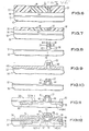
- Fig. 1-12 are flow diagrams illustrating by sequential cross-sectional representation the process steps of the present invention culminating in the self-aligned, submicron GaAs gate FET structure shown in Fig. 12.
- a fast-switching insulated GaAs-gate N-channel FET formed on an undoped GaAs substrate 10.
- the GaAs gate 40 is highly N doped and is of submicron length (e.g., 0,4-0,5 ⁇ m).
- Metal 32 precisely overlying the gate 40 provides a low resistance ohmic contact to the gate electrode 40.
- An undoped AlGaAs 12 forms the gate insulator.
- N type source 52 and drain 54 are formed in the substrate 10 at a precise predetermined submicron spacing (e.g., 0,1-0,3 ⁇ m) from and self aligned with the vertical edges 42 and 44 of gate 40, respectively.
- the submicron spacing is achieved by means of sidewall insulator 48 abutting the gate 40.
- 58 and 60 represent conductive metallization establishing ohmic contacts with source 52 and drain 54, respectively.
- the Fig. 12 structure also shows optional device isolation regions 55 if the semi insulating GaAs substrate 10 is not able to provide the required device isolation.
- Figs 1-12 illustrate sequential steps in the fabrication of the self-aligned GaAs-gate FET device with submicron channel length in accordance with the process of the present invention.
- a semi-insulating GaAs wafer (not shown)
- a thick (typically, about 1 ⁇ m thickness) buffer or substrate layer 10 of undoped GaAs is formed thereon.
- a relatively thin undoped AlGaAs layer 12 is formed over the GaAs substrate 10.
- the AlGaAs layer 12 serves as the gate insulator for the FET device. Since neither the thickness nor the mole fraction of aluminum in AlGaAs gate insulator determine the threshhold voltage, their precise values are, to a first order, inconsequential.
- the thickness of insulator layer 12 is in the range of about 200-300 Angstroms.
- a typical aluminum mole fraction is that given by Al 0,4 Ga 0,6 As.
- a highly N doped GaAs layer 14 of thickness 0,2-0,3 ⁇ m is formed thereon.
- Typical N type dopant used for doping the layer 14 is silicon.
- the dopant concentration in the GaAs layer 14 is governed by the required near-zero threshold voltage of the device. For a Vth of about 0.1 V, the preferred dopant concentration is about 1 ⁇ 1018 atoms/cc.
- the layers 10, 12 and 14 may be formed by a conventional process such as molecular beam epitaxy (MBE) or metal organic chemical vapor deposition (MOCVD).
- the SixNy layer is formed by plasma enhanced CVD using a gas mixture of silane and ammonia.
- the SixNy and photoresist layers are patterned into a substantially vertical-walled island or mandrel 16 composed of photoresist layer 18 and SixNy layer 20.
- the SixNy and photoresist layers are etched by RIE.
- CF4 is used for etching SixNy and O2 for etching the photoresist.
- the basic purpose of the SixNy layer 20, as will become more apparent later on, is to serve as an etchstop during a subsequent etching step.
- the next step is to form a controlled, submicron thick metal layer on the sidewalls 22 and 24 of the mandrel 16.
- This is preferably accomplished by forming a conformal layer 26 of a metal by sputtering, E-beam evaporation or ion-beam deposition, as illustrated in Fig. 2.
- a conformal layer 26 of a metal by sputtering, E-beam evaporation or ion-beam deposition, as illustrated in Fig. 2.
- This metal should be compatible with the N+ GaAs gate material in terms of adhesion, etc.
- a refractory metal will be suitable in view of the relatively high temperature annealing heat cycle which follows later.
- Molybdenum and molybdenum-germanium are suitable metals. Since the thickness of the metal layer 26 will eventually determine the FET channel length, to obtain submicron channel length, the thickness of layer 26 should be correspondingly chosen to be submicron. Typical thickness of layer 26 is in the
- the layer 26 is subjected to anisotropic etching to substantilly remove the layer from all substantially horizontal surfaces and leave the sidewall layer 28 on the substantially vertical surfaces 22 and 24 of the photoresist mandrel 16.
- RIE in CF4 plasma may be used if the metal 26 is molybdenum.
- unwanted portion of the metal sidewall 28 is removed, leaving the metal sidewall only in the area corresponding to the desired GaAs gate width.
- the resulting structure is depicted in Fig. 4.
- a relatively thick (typical thickness 1,5-2,0 ⁇ m) layer 30 of a viscous organic material is applied to planarize the structure.
- Suitable materials for this planarization purpose include polyimide and photoresist. If photoresist or polyimide is used for planarization, it is applied by spin coating followed by hardening.
- the planarized structure is then subjected to RIE, typically, in O2 plasma in order to etch off the layer 30 down to the surface of the SixNy dielectric layer 20 as illustrated in Fig. 6.
- the SixNy layer 20 serves as an etch stop as previously noted. The etching is then continued as illustrated in Fig.
- CF4 etchant gas to controllably remove the SixNy layer 20 and further etch back the upper surface portions of the metal sidewall 18, until the metal 18 is reduced to a sufficiently thin strip 32 with substantially vertical edges.
- the thickness of the remnant metal 32 is sufficiently large so as to eventually provide a low resistance path above the GaAs gate. Typical thickness of the metal strip 32 is in the range of about 0,2-0,35 ⁇ m.
- the CF4 etch back is accomplished by time-controlled RIE. During this metal etch back process step, the upper surface portions of the layers 18 and 30 are also removed at practically the same etch rate. Thereafter, the remaining portions of photoresist 18 and 30 are removed by conventional ashing, leaving a free-standing and well-delineated metal strip 32 having essentially vertical walls 34 and 36 and horizontal top surface 38.
- the underlying N+ GaAs layer 14 is defined into a GaAs gate 40 of submicron width W as depicted in Fig. 8.
- This gate definition is accomplished by RIE using, for example, a gas mixture of CCl2F2 and helium. Since the metal mask is provided with substantially vertical walls 34 and 36, the GaAs gate 40 defined by transferring the wall profile of the metal 32 to the layer 14 will also have substantially vertical walls 42 and 44 as illustrated in Fig. 8. In this manner, a structure composed of a submicron wide GaAs gate having atop thereof a metal strip of identically equal width is formed in a precisely controlled manner above the AlGaAs layer 12.
- an insulator spacer abutting the composite gate structure 32-40 is formed.
- a conformal insulator layer 46 such as silicon dioxide or SiOx is formed covering the gate structure 32-40 and the exposed insulator layer 12.
- the layer 46 is typically formed by CVD at a low temperature of 300-400°C.
- the thickness of the oxide 46 is dictated by the desired lateral spacing of the source/drain regions with respect to the gate. Typically, the thickness of the layer 46 is in the range 0,1-0,3 ⁇ m.
- a photoresist mask 50 is formed on the AlGaAs layer 12 to cover all regions of this layer except the gate regions and those in correspondence with the regions where the transistor source and drain regions are to be formed.
- N type ion implantation across the exposed AlGaAs layer 12 N+ source 52 and drain 54 are formed in the undoped GaAs substrate 10 in a self-aligned relationship with the gate structure 32-40.
- the particular combination of the implantation species, dose and energy is governed by the desired junction depth of the source/drain regions. This combination is selected such that the source/drain junction depth is large enough to provide minimum source/drain series resistance, but small enough to minimize the capacitance arising from the gate to the source/drain.
- Typical dopant for ion implantation of source 52 and drain 54 is silicon (Si+) at a dose of about (2-4) ⁇ 1013 ions/sq. cm. and energy of 80-100 Kev to attain a junction depth of 0,2-0,25 ⁇ m.
- the resist mask 50, the gate structure 32-40 and the associated sidewall insulator spacers 48 provide the selectivity in forming the Nsource 52 and drain 54 exactly as desired.
- the source 52 and drain 54 are situated precisely 0,1-0,3 ⁇ m away from the edges of the GaAs gate 40, a distance corresponding to the thickness of the insulator sidewall 48.
- the photoresist 50 is stripped off and the structure is subjected to an annealing process to remove the damage to the GaAs substrate 10 caused during the source/drain ion implantation.
- One annealing process is capless arsine annealing at a temperature in the range 750°C to 825°C for about 10 minutes.
- Another annealing method is flash anneal using an infrared or halogen lamp at a temperature of about 750-800°C for a duration of about 2-30 seconds.
- isolation 54 between devices is then established, if desired, by utilizing a suitable mask and implanting boron ions at a high dose and energy.
- the isolation regions 54 typically extend to a depth of about 0,5 ⁇ m.
- a passivation layer 56 of, for example, silicon dioxide is formed followed by making contact openings therein in correspondence with the source 52, drain 54 and gate 32-40 (gate contact opening is not shown in Fig. 12 due to its cross sectional representation).
- the AlGaAs layer 12 exposed by the source/drain contact openings is then removed.
- a contact metal such as gold-germanium-nickel of about 0,1-0,3 ⁇ m thickness is formed at all contact openings.
- the source and drain contact metal patterns formed in this manner are designated by 58 and 60, respectively.
- the contact metallurgy is preferably formed by evaporation. For forming good ohmic contacts, the contact metallurgy is annealed at a temperature of about 400-450 °C for 50-120 seconds. Alternatively, laser annealing may be utilized for reducing the contact resistance.
- the GaAs-gate heterojunction FET fabricated in accordance with the process steps illustrated in Figs. 1-12 has its source 52 and drain 54 in close proximity and at the two flanks of the composite gate 32-40.
- This self-aligned FET structure is characterized by a short submicron channel length that has both substantially reduced channel resistance and accompanying parasitic gate-to-channel capacitance.
- the device structure also has a minimum geometry because the composite gate 32-40 is of submicron width and the source 52 and drain 54 are defined by minimum lithography feature size.
- the self-aligned GaAs-gate FETs made in accordance with this novel and unobvious method do not have the undesirable performance limitations imposed by heretofore device structures having longer channel lengths and larger device size.
- a submicron self-aligned GaAs-gate FET can be made by the method disclosed herein utilizing only conventional photolithography which may not provide feature sizes less than about 1,5-2,0 ⁇ m.
- This new process is inherently simple and is capable of supporting a high level of circuit integration. This aspect is important because a simple process which supports a high level of integration contributes directly to yield, reliability and cost improvement.
Abstract
Description
- The invention relates to gallium arsenide (GaAs) integrated circuit fabrication technology, and more particularly, to a method of forming on a GaAs substrate an insulated GaAs-gate field effect transistor (FET) having self-aligned source/drain and submicron channel length.
- Since the mobility of electrons is substantially higher in GaAs than in silicon, higher integrated circuit performance can be achieved using GaAs as the substrate material compared to silicon for an equivalent power consumption. A number of transistor types have been built using GaAs material. The most common and commercially successful type is the metal-semiconductor field effect transistor (MESFET). This device comes in two forms: the depletion mode MESFET (D MESFET) and the enhancement mode MESFET (E-MESFET). The basic MESFET consists of a metal Schottky gate placed between a source and a drain region. The transistor typically is formed in two ionimplantation steps: a relatively low concentration implant below the gate region provides the channel, and a relatively high concentration implant in close vicinity to the gate provides the source and the drain regions. In a D-MESFET, with no voltage applied to the gate, current flows through the channel between the transistor's source and drain when a voltage is applied across the source and drain. The application of a gate voltage (negative with respect to the source) causes the channel to become narrower, reducing current flow. If a sufficiently negative gate voltage is applied, the current flow is pinched off. In an E-MESFET, the region under the gate is doped such that the channel is pinched off when no gate voltage is applied. A small positive gate voltage with respect to the source will initiate current flow.
- Another GaAs device that has shown potential for commercialization is the high electron mobility transistor (HEMT). This structure has also been termed as the selectively doped heterojunction transistor (SDHT), modulation doped FET (MODFET) and two-dimensional electron gas FET (TEGFET). These are superlattice heterojunctions in which layers of gallium-aluminum-arsenide (AlGaAs) are typically deposited on an undoped GaAs channel. One such device was disclosed in an article by T. Mimura et al, entitled "A New Field Effect Transistor with Selectively Doped GaAs/-n-GaAlx-As1- x Heterojunctions", Japanese Journal of Applied Physics, Vol. 19. No. 5, pages L225-227 (May 1980). The device described in this article consists of a pair of undoped GaAs layers sandwiching a layer of silicon doped GaAlAs. A Schottky gate is provided by the deposition of aluminum on the surface of the top undoped GaAs layer. Electron mobility in a HEMT is higher than a MESFET as the charge carriers are not scattered by dopant ions in the channel. By raising gate voltage just above the threshold, a HEMT quickly reaches its full transconductance, giving it a very fast turnon time. However, the threshold voltage of a HEMT is neither as controllable nor as low as is desirable for logic circuits with reduced power supply voltages. The threshhold variability is due to its sensitivity to the doping and thickness of the active layer. Also, the particular layered structure of the HEMT in combination with the Schottky contact to the top results in a threshold voltage which departs significantly from the desired near-zero value.
- To overcome the deficiencies of the HEMT, a new semiconductor-insulator-semiconductor transistor has been proposed in U.S.-A Serial No.4,583,105 entitled "A Double Heterojunction FET with Ohmic Semiconductor Gate and Controllable Low Threshold Voltage" by J. Rosenerg which is assigned to IBM Corporation, the present assignee. This structure consists of a heavily doped n-type GaAs gate with undoped AlGaAs as the gate insulator, on an undoped GaAs layer. Threshold voltage of this device structure is naturally near zero since the work function difference between the doped GaAs gate and the undoped GaAs is essentially zero. This structure is well suited for low-voltage logic applications. Another advantage of this structure is that, at least to first order, its threshold voltage is independent of the thickness and aluminum mole fraction of the AlGaAs layer. This undoped heterojunction structure is inherently more resistant to high-temperature annealing, not suffering from a field-enhanced degradation of the hetero-junction due to ionized impurities.
- Despite these advantageous features of the GaAs-gate heterojunction FET, the prior art methods of fabrication provided a structure having a rather large gate length. For example, the article by P. M. Solomon et al, entitled "A GaAs Gate Heterojunction FET", IEEE Electron Device Letters, Vol. EDL-5, No. 9, pages 379-381, September 1984 discloses an N type GaAs-gate FET having a gate length of 1,5 µm. The article by K. Matsumoto et al, entitled "n+ GaAs/Undoped GaAlAs/Undoped GaAs Field-Effect Transistor" Electronics Letters, 1984, 20, pages 462-463 discloses a method of forming a GaAs gate of length 2 mLikewise, the article by K. Matsumoto et al, entitled "p-Channel GaAs SIS (Semiconductor-Insulator-Semiconductor) FET", Electronics Letters, 1985, 21, pages 580-581 discloses a P channel GaAs gate FET having a gate length of 2 µ m. The basic reason for such large dimensioned gate structures is that these prior art methods utilize standard photolithography and etching techniques to form the gate. These methods are thus not suitable for fabrication of submicron-length gate structures that are demanded by high-density and speed GaAs memory and logic circuits. Another shortcoming of some of these prior art structures is that the metal contact to the GaAs gate tends to be sufficiently away so as to appreciably increase gate resistance. Yet another disadvantage is that these prior art methods obtain a structure wherein the source/drain is either too far away from the gate, leading to increased source/drain resistance, or too close to the gate leading to increased gate-source/drain overlap capacitance. From a performance standpoint it is imperative that the source/drain be located at an optimal distance from the gate which permits minimization of both source/drain resistance and gate-source/drain overlap capacitance. As device dimensions shrink to submicron dimensions, this optimization becomes even more important.
- It would appear that a submicron-length GaAs gate FET may be realized by utilizing submicron E-beam lithography to define the gate. However, existing E-beam systems require an E-beam pattern generator, sophisticated E-beam optics and custom software to control, all of which render this technique prohibitively expensive.
- Accordingly, it is an object of the present invention to provide a method of forming a GaAs-gate heterojunction FET which has submicron-length gate and self-aligned metal contacting the gate.
- Another object of the invention is to provide a method of forming a high-speed GaAs-gate FET by minimizing the source/drain resistance and gate source/drain capacitance.
- The invention is a process of forming a high speed, submicron gate-length, self-aligned GaAs-gate FET device. Starting with an undoped GaAs substrate having successively formed layers of undoped GaAlAs and highly doped (e.g., N type) GaAs, a submicron-wide metal contacting the doped GaAs layer is formed utilizing sidewall image transfer technique. This technique includes forming on the doped GaAs a mandrel of a suitable material (e.g., photoresist) having substantially vertical and horizontal surfaces; depositing on the mandrel a conformal, submicron thick (0,4-0,5 µ m) highly conductive layer of a suitable metal; establishing through RIE submicron-wide metal sidewalls along the vertical sides of the mandrel; removing the unwanted portion of the metal by a photomasking operation; coating a thick layer of a planarizing material (e.g., photoresist); etching back by RIE the upper portions of the resulting structure until the metal sidewall is transformed into a metal strip having substantially vertical walls and a substantially horizontal surface; and removing the remnant planarizing material and the mandrel material.
- Using the submicron-wide metal as a mask, the doped GaAs is patterned into a gate for the FET having the characteristics of submicron length, substantially vertical surfaces and fully contacted metal on the top. Next, a conformal layer of an insulator (e.g., SiOx) of submicron thickness (0,1-0,3 µ m) is formed at a low temperature. This is followed by RIE to remove the insulator from the horizontal surfaces, leaving submicron-wide insulator spacers abutting the gate structure. By means of ion implantation across the exposed AlGaAs layer, source and drain are formed in the undoped GaAs substrate in a self-aligned fashion with respect to the gate structure. The AlGaAs layer beneath the doped GaAs gate serves as the gate insulator. Damage caused to the GaAs substrate as a result of the ion implantation step is removed by annealing. The ion implantation species, dose, energy, and annealing process are chosen such as to achieve a source/drain junction depth large enough to minimize the source/drain series resistance, but small enough to minimize the parasitic capacitance of the gate to the source/drain. Finally, conductive electrical contacts are established with the source/drain and gate by forming a passivation layer, making contact openings therein, and depositing and delineating a suitable metal.
- The novel features, process steps and their combination which are characteristic of the invention are set forth in the appended claims. The invention, however, will be best understood by reference to the detailed description which follows in conjunction with the accompanying drawings wherein:
- Fig. 1-12 are flow diagrams illustrating by sequential cross-sectional representation the process steps of the present invention culminating in the self-aligned, submicron GaAs gate FET structure shown in Fig. 12.
- Referring now to Fig. 12, there is shown in this figure a fast-switching insulated GaAs-gate N-channel FET formed on an
undoped GaAs substrate 10. The GaAsgate 40 is highly N doped and is of submicron length (e.g., 0,4-0,5 µ m).Metal 32 precisely overlying thegate 40 provides a low resistance ohmic contact to thegate electrode 40. An undoped AlGaAs 12 forms the gate insulator.N type source 52 anddrain 54 are formed in thesubstrate 10 at a precise predetermined submicron spacing (e.g., 0,1-0,3 µ m) from and self aligned with thevertical edges gate 40, respectively. The submicron spacing is achieved by means ofsidewall insulator 48 abutting thegate 40. 58 and 60 represent conductive metallization establishing ohmic contacts withsource 52 anddrain 54, respectively. The Fig. 12 structure also shows optionaldevice isolation regions 55 if the semi insulatingGaAs substrate 10 is not able to provide the required device isolation. - Figs 1-12 illustrate sequential steps in the fabrication of the self-aligned GaAs-gate FET device with submicron channel length in accordance with the process of the present invention. Referring to Fig. 1, starting with a semi-insulating GaAs wafer (not shown), a thick (typically, about 1 µ m thickness) buffer or
substrate layer 10 of undoped GaAs is formed thereon. Next a relatively thinundoped AlGaAs layer 12 is formed over theGaAs substrate 10. TheAlGaAs layer 12 serves as the gate insulator for the FET device. Since neither the thickness nor the mole fraction of aluminum in AlGaAs gate insulator determine the threshhold voltage, their precise values are, to a first order, inconsequential. Typically, the thickness ofinsulator layer 12 is in the range of about 200-300 Angstroms. A typical aluminum mole fraction is that given by Al0,4 Ga0,6 As. Following the growth of theAlGaAs layer 12, a highly N dopedGaAs layer 14 of thickness 0,2-0,3 µ m is formed thereon. Typical N type dopant used for doping thelayer 14 is silicon. The dopant concentration in theGaAs layer 14 is governed by the required near-zero threshold voltage of the device. For a Vth of about 0.1 V, the preferred dopant concentration is about 1×10¹⁸ atoms/cc. Thelayers - Continuing with the structure of Fig. 1, a
blanket layer 18 of photoresist, typically about 1 µ m thickness, is formed next by conventional spin coating or spraying, followed by baking. Thereafter, about 0,1-0,15 µ mthickness layer 20 of a dielectric material such as SixNy (x and y are arbitrary numbers, for example x=3 and y=4) is formed over thephotoresist layer 18. Preferably, the SixNy layer is formed by plasma enhanced CVD using a gas mixture of silane and ammonia. Then, by standard lithography and etching, the SixNy and photoresist layers are patterned into a substantially vertical-walled island ormandrel 16 composed ofphotoresist layer 18 andSixNy layer 20. To obtain the substantiallyvertical mandrel walls SixNy layer 20, as will become more apparent later on, is to serve as an etchstop during a subsequent etching step. - The next step is to form a controlled, submicron thick metal layer on the
sidewalls mandrel 16. This is preferably accomplished by forming aconformal layer 26 of a metal by sputtering, E-beam evaporation or ion-beam deposition, as illustrated in Fig. 2. Regardless of which method of forming thelayer 26 is selected, it is accomplished at a low temperature less than about 300°C. This metal should be compatible with the N+ GaAs gate material in terms of adhesion, etc. In general, a refractory metal will be suitable in view of the relatively high temperature annealing heat cycle which follows later. Molybdenum and molybdenum-germanium are suitable metals. Since the thickness of themetal layer 26 will eventually determine the FET channel length, to obtain submicron channel length, the thickness oflayer 26 should be correspondingly chosen to be submicron. Typical thickness oflayer 26 is in the range of about 0,3-0,5 µ m. - Next, referring to Fig. 3, the
layer 26 is subjected to anisotropic etching to substantilly remove the layer from all substantially horizontal surfaces and leave thesidewall layer 28 on the substantiallyvertical surfaces photoresist mandrel 16. RIE in CF4 plasma may be used if themetal 26 is molybdenum. Thereafter, by using standard photolithographic masking and etching steps, unwanted portion of themetal sidewall 28 is removed, leaving the metal sidewall only in the area corresponding to the desired GaAs gate width. The resulting structure is depicted in Fig. 4. - Progressing toward the structure of Fig. 5, next a relatively thick (typical thickness 1,5-2,0 µ m)
layer 30 of a viscous organic material is applied to planarize the structure. Suitable materials for this planarization purpose include polyimide and photoresist. If photoresist or polyimide is used for planarization, it is applied by spin coating followed by hardening. The planarized structure is then subjected to RIE, typically, in O₂ plasma in order to etch off thelayer 30 down to the surface of theSixNy dielectric layer 20 as illustrated in Fig. 6. In this connection, theSixNy layer 20 serves as an etch stop as previously noted. The etching is then continued as illustrated in Fig. 7 by switching to CF4 etchant gas to controllably remove theSixNy layer 20 and further etch back the upper surface portions of themetal sidewall 18, until themetal 18 is reduced to a sufficientlythin strip 32 with substantially vertical edges. The thickness of theremnant metal 32 is sufficiently large so as to eventually provide a low resistance path above the GaAs gate. Typical thickness of themetal strip 32 is in the range of about 0,2-0,35 µ m. The CF4 etch back is accomplished by time-controlled RIE. During this metal etch back process step, the upper surface portions of thelayers photoresist metal strip 32 having essentiallyvertical walls top surface 38. - Next, using the
metal strip 32 as a mask, the underlyingN+ GaAs layer 14 is defined into aGaAs gate 40 of submicron width W as depicted in Fig. 8. This gate definition is accomplished by RIE using, for example, a gas mixture of CCl2F2 and helium. Since the metal mask is provided with substantiallyvertical walls GaAs gate 40 defined by transferring the wall profile of themetal 32 to thelayer 14 will also have substantiallyvertical walls AlGaAs layer 12. - Next, as illustrated in Figs. 9-10, an insulator spacer abutting the composite gate structure 32-40 is formed. To achieve this end result, a
conformal insulator layer 46 such as silicon dioxide or SiOx is formed covering the gate structure 32-40 and the exposedinsulator layer 12. Thelayer 46 is typically formed by CVD at a low temperature of 300-400°C. The thickness of theoxide 46 is dictated by the desired lateral spacing of the source/drain regions with respect to the gate. Typically, the thickness of thelayer 46 is in the range 0,1-0,3 µ m. By subjecting thelayer 46 to RIE, it is removed from the horizontal surfaces, leaving thesidewall layer 48 on the substantially vertical surfaces of the composite gate structure 32-40 as shown in Fig. 10. If SiOx is used as theinsulator 46, then CF4 would be a suitable RIE gas. - Next, referring to Fig. 11, a
photoresist mask 50 is formed on theAlGaAs layer 12 to cover all regions of this layer except the gate regions and those in correspondence with the regions where the transistor source and drain regions are to be formed. Then, by N type ion implantation across the exposedAlGaAs layer 12,N+ source 52 and drain 54 are formed in theundoped GaAs substrate 10 in a self-aligned relationship with the gate structure 32-40. The particular combination of the implantation species, dose and energy is governed by the desired junction depth of the source/drain regions. This combination is selected such that the source/drain junction depth is large enough to provide minimum source/drain series resistance, but small enough to minimize the capacitance arising from the gate to the source/drain. Typical dopant for ion implantation ofsource 52 and drain 54 is silicon (Si+) at a dose of about (2-4)×1013 ions/sq. cm. and energy of 80-100 Kev to attain a junction depth of 0,2-0,25 µ m. The resistmask 50, the gate structure 32-40 and the associatedsidewall insulator spacers 48 provide the selectivity in forming theNsource 52 and drain 54 exactly as desired. In particular, thesource 52 and drain 54 are situated precisely 0,1-0,3 µ m away from the edges of theGaAs gate 40, a distance corresponding to the thickness of theinsulator sidewall 48. - Continuing with the process steps pertaining to Fig. 11, the
photoresist 50 is stripped off and the structure is subjected to an annealing process to remove the damage to theGaAs substrate 10 caused during the source/drain ion implantation. One annealing process is capless arsine annealing at a temperature in the range 750°C to 825°C for about 10 minutes. Another annealing method is flash anneal using an infrared or halogen lamp at a temperature of about 750-800°C for a duration of about 2-30 seconds. - To prevent electrical leakage,
isolation 54 between devices is then established, if desired, by utilizing a suitable mask and implanting boron ions at a high dose and energy. Theisolation regions 54 typically extend to a depth of about 0,5µ m. - Turning to Fig 12, next a
passivation layer 56 of, for example, silicon dioxide is formed followed by making contact openings therein in correspondence with thesource 52, drain 54 and gate 32-40 (gate contact opening is not shown in Fig. 12 due to its cross sectional representation). TheAlGaAs layer 12 exposed by the source/drain contact openings is then removed. Using a lift-off stencil, a contact metal such as gold-germanium-nickel of about 0,1-0,3 µ m thickness is formed at all contact openings. The source and drain contact metal patterns formed in this manner are designated by 58 and 60, respectively. The contact metallurgy is preferably formed by evaporation. For forming good ohmic contacts, the contact metallurgy is annealed at a temperature of about 400-450 °C for 50-120 seconds. Alternatively, laser annealing may be utilized for reducing the contact resistance. - As is apparent from the foregoing description, the GaAs-gate heterojunction FET fabricated in accordance with the process steps illustrated in Figs. 1-12 has its
source 52 and drain 54 in close proximity and at the two flanks of the composite gate 32-40. This self-aligned FET structure is characterized by a short submicron channel length that has both substantially reduced channel resistance and accompanying parasitic gate-to-channel capacitance. The device structure also has a minimum geometry because the composite gate 32-40 is of submicron width and thesource 52 and drain 54 are defined by minimum lithography feature size. Thus, the self-aligned GaAs-gate FETs made in accordance with this novel and unobvious method do not have the undesirable performance limitations imposed by heretofore device structures having longer channel lengths and larger device size. It is important to note and appreciate that a submicron self-aligned GaAs-gate FET can be made by the method disclosed herein utilizing only conventional photolithography which may not provide feature sizes less than about 1,5-2,0 µ m. This new process is inherently simple and is capable of supporting a high level of circuit integration. This aspect is important because a simple process which supports a high level of integration contributes directly to yield, reliability and cost improvement. - Thus, there has been provided, in accordance with the invention, a novel process that fully satisfies the objects and advantages set forth.
- While the invention has been described in conjunction with a specific preferred embodiment, it is evident that many alternatives, modifications and variations will be apparent to those skilled in the art in light of the foregoing description. It is therefore contemplated that the appended claims will embrace any such alternatives, modifications, variations as fall within the true scope and spirit of the invention.
Claims (16)
depositing a submicron thickness insulator layer on the structure resulting at the completion of step (c); and
anisotropically etching said submicron thickness insulator layer to leave controlled submicron thickness insulator layer on the walls of said gate and said contact.
providing a GaAs substrate having a relatively thin layer of AlGaAs thereon and a relatively thick doped GaAs layer on said AlGaAs layer;
forming a conductive strip having submicrometer width and thickness dimensions on said doped GaAs layer, the width of said strip corresponding to the channel length of said FET;
etching said doped GaAs layer using said strip as a mask to form a GaAs gate having substantially vertical walls and width identically matching with the width of said strip, said strip serving as a self-aligned conductive contact to said gate;
forming a controlled submicrometer thickness layer on the vertical walls of said gate and said contact; and forming source and drain regions in said substrate using the said gate and said layer on said walls of said gate and said contact as a mask in a self-aligned relationship with said gate.
forming a first removable layer having a substantially vertical surface on said doped GaAs layer;
forming a controlled submicrometer thickness conductive layer on the vertical surface of said first removable layer;
coating the resulting structure with a thick second removable layer thereby obtaining a planarized structure composed of said first and second removable layers and said conductive layer;
uniformly etching back the planarized structure to remove the upper portions of said first and second removable layers and conductive layer, thereby transforming said conductive layer into said strip embedded in said first and second removable layers remaining at the completion of the present etchback step;
removing said remaining first and second removable layers.
depositing a conformal layer of said insulative material; and anisotropically etching said conformal layer to remove said conformal layer from everywhere except from said vertical walls of said gate and said contact.
providing a semi-insulating GaAs substrate having
a gate insulating layer of AlGaAs thereon and a thicker highly doped GaAs layer on said AlGaAs layer;
forming a layer of an organic material having substantially vertical surfaces and a substantially horizontal surface on said doped GaAs layer;
forming a conformal submicron thickness conductive layer on said organic layer and said doped GaAs layer not masked by said organic layer;
anisotropically etching said conformal conductive layer to remove said conductive layer from horizontal surfaces and leave said conductive layer on said substantially vertical surfaces;
removing the undesired portions of said conductive layer on said vertical surfaces;
applying a thick removable layer on the resulting structure thereby obtaining a planarized structure composed of said thick removable layer, said layer of organic material and conductive layer on selected portions of said vertical surfaces;
uniformly etching back said planarized structure to transform said conductive layer on selected portions of said vertical surfaces into a conductive strip of submicron thickness and width while simultaneously removing the upper surface portions of said removable layer and said layer of organic material;
using said conductive strip as a mask, etching to transform said doped GaAs layer into a GaAs gate having a width identical to that of said strip, said strip serving as self-aligned contact to said gate, said gate and said contact having substantially vertical sidewalls;
forming a controlled submicron thick insulative layer on the said sidewalls of said gate and contact; and
forming source and drain regions in said substrate by ion implantation through said AlGaAs layer using said gate in combination with said sidewalls as a mask, said source and drain being self-aligned to said gate.
applying a layer of photoresist to said doped GaAs layer;
depositing a SixNy layer on said photoresist;
patterning, by photolithography and etching, said SixNy layer into a desired pattern; and
using the patterned SixNy layer as a mask, etching said photoresist.
reactive ion etching in oxygen plasma utilizing said SixNy layer as an etch stop; and
reactive ion etching in CF4 plasma for a predetermined period of time to obtain said strip of submicron thickness.
Applications Claiming Priority (2)
| Application Number | Priority Date | Filing Date | Title |
|---|---|---|---|
| US06/848,874 US4689869A (en) | 1986-04-07 | 1986-04-07 | Fabrication of insulated gate gallium arsenide FET with self-aligned source/drain and submicron channel length |
| US848874 | 1986-04-07 |
Publications (2)
| Publication Number | Publication Date |
|---|---|
| EP0240683A1 true EP0240683A1 (en) | 1987-10-14 |
| EP0240683B1 EP0240683B1 (en) | 1993-01-20 |
Family
ID=25304516
Family Applications (1)
| Application Number | Title | Priority Date | Filing Date |
|---|---|---|---|
| EP87102621A Expired - Lifetime EP0240683B1 (en) | 1986-04-07 | 1987-02-24 | Fabrication of insulated gallium arsenide-gate fet with self-aligned source/drain and submicron channel length |
Country Status (4)
| Country | Link |
|---|---|
| US (1) | US4689869A (en) |
| EP (1) | EP0240683B1 (en) |
| JP (1) | JP2599381B2 (en) |
| DE (1) | DE3783635T2 (en) |
Cited By (3)
| Publication number | Priority date | Publication date | Assignee | Title |
|---|---|---|---|---|
| EP0336660A1 (en) * | 1988-04-08 | 1989-10-11 | AT&T Corp. | Semiconductor devices having multi-level metal interconnects |
| US6790717B2 (en) | 2001-01-17 | 2004-09-14 | United Monolithic Semiconductors Gmbh | Method for producing a semiconductor component comprising a t-shaped contact electrode |
| DE102007026879A1 (en) * | 2007-05-29 | 2008-12-18 | Qimonda Ag | Method for producing a structure on or in a substrate, imaging layer for producing sub-lithographic structures, method for inverting a sub-lithographic pattern, device obtainable by producing a structure |
Families Citing this family (30)
| Publication number | Priority date | Publication date | Assignee | Title |
|---|---|---|---|---|
| US5834793A (en) * | 1985-12-27 | 1998-11-10 | Kabushiki Kaisha Toshiba | Semiconductor devices |
| JPS63207177A (en) * | 1987-02-24 | 1988-08-26 | Toshiba Corp | Manufacture of semiconductor device |
| US4847674A (en) * | 1987-03-10 | 1989-07-11 | Advanced Micro Devices, Inc. | High speed interconnect system with refractory non-dogbone contacts and an active electromigration suppression mechanism |
| US4914500A (en) * | 1987-12-04 | 1990-04-03 | At&T Bell Laboratories | Method for fabricating semiconductor devices which include sources and drains having metal-containing material regions, and the resulting devices |
| EP0416141A1 (en) * | 1989-09-04 | 1991-03-13 | Siemens Aktiengesellschaft | Process for manufacturing an FET having an asymmetrically positioned gate region |
| US5024971A (en) * | 1990-08-20 | 1991-06-18 | Motorola, Inc. | Method for patterning submicron openings using an image reversal layer of material |
| US5227320A (en) * | 1991-09-10 | 1993-07-13 | Vlsi Technology, Inc. | Method for producing gate overlapped lightly doped drain (goldd) structure for submicron transistor |
| US5147812A (en) * | 1992-04-01 | 1992-09-15 | Motorola, Inc. | Fabrication method for a sub-micron geometry semiconductor device |
| US5250454A (en) * | 1992-12-10 | 1993-10-05 | Allied Signal Inc. | Method for forming thickened source/drain contact regions for field effect transistors |
| JPH09139495A (en) * | 1995-11-14 | 1997-05-27 | Nippon Steel Corp | Semiconductor device and its manufacture |
| US5599738A (en) * | 1995-12-11 | 1997-02-04 | Motorola | Methods of fabrication of submicron features in semiconductor devices |
| DE19548058C2 (en) * | 1995-12-21 | 1997-11-20 | Siemens Ag | Method of manufacturing a MOS transistor |
| KR19980078235A (en) * | 1997-04-25 | 1998-11-16 | 문정환 | Manufacturing Method of Semiconductor Device |
| US6214678B1 (en) * | 1997-05-21 | 2001-04-10 | Hughes Electronics Corp | Growth technique for low noise high electron mobility transistors by metal organic vapor phase epitaxy |
| US6372590B1 (en) | 1997-10-15 | 2002-04-16 | Advanced Micro Devices, Inc. | Method for making transistor having reduced series resistance |
| US6326794B1 (en) | 1999-01-14 | 2001-12-04 | International Business Machines Corporation | Method and apparatus for in-situ monitoring of ion energy distribution for endpoint detection via capacitance measurement |
| US6509219B2 (en) | 2001-03-19 | 2003-01-21 | International Business Machines Corporation | Fabrication of notched gates by passivating partially etched gate sidewalls and then using an isotropic etch |
| US6528363B2 (en) | 2001-03-19 | 2003-03-04 | International Business Machines Corporation | Fabrication of notched gates by passivating partially etched gate sidewalls and then using an isotropic etch |
| WO2003032397A2 (en) | 2001-07-24 | 2003-04-17 | Cree, Inc. | INSULTING GATE AlGaN/GaN HEMT |
| US6541320B2 (en) | 2001-08-10 | 2003-04-01 | International Business Machines Corporation | Method to controllably form notched polysilicon gate structures |
| US6833556B2 (en) * | 2002-08-12 | 2004-12-21 | Acorn Technologies, Inc. | Insulated gate field effect transistor having passivated schottky barriers to the channel |
| US7084423B2 (en) | 2002-08-12 | 2006-08-01 | Acorn Technologies, Inc. | Method for depinning the Fermi level of a semiconductor at an electrical junction and devices incorporating such junctions |
| US7692263B2 (en) | 2006-11-21 | 2010-04-06 | Cree, Inc. | High voltage GaN transistors |
| US8691697B2 (en) | 2010-11-11 | 2014-04-08 | International Business Machines Corporation | Self-aligned devices and methods of manufacture |
| US8557675B2 (en) | 2011-11-28 | 2013-10-15 | Globalfoundries Inc. | Methods of patterning features in a structure using multiple sidewall image transfer technique |
| US8669186B2 (en) | 2012-01-26 | 2014-03-11 | Globalfoundries Inc. | Methods of forming SRAM devices using sidewall image transfer techniques |
| US9620611B1 (en) | 2016-06-17 | 2017-04-11 | Acorn Technology, Inc. | MIS contact structure with metal oxide conductor |
| WO2018094205A1 (en) | 2016-11-18 | 2018-05-24 | Acorn Technologies, Inc. | Nanowire transistor with source and drain induced by electrical contacts with negative schottky barrier height |
| US10850462B2 (en) * | 2018-10-03 | 2020-12-01 | Visera Technologies Company Limited | Optical elements and method for fabricating the same |
| CN112928153B (en) * | 2019-12-05 | 2023-07-04 | 中芯国际集成电路制造(天津)有限公司 | Semiconductor structure and forming method thereof |
Citations (5)
| Publication number | Priority date | Publication date | Assignee | Title |
|---|---|---|---|---|
| GB2003660A (en) * | 1977-08-19 | 1979-03-14 | Plessey Co Ltd | Deposition of material on a substrate |
| EP0083785A2 (en) * | 1981-12-30 | 1983-07-20 | International Business Machines Corporation | Method of forming self-aligned field effect transistors in integrated circuit structures |
| EP0098775A2 (en) * | 1982-07-01 | 1984-01-18 | Commissariat A L'energie Atomique | Process for making an integrated-circuit field oxide |
| EP0114962A2 (en) * | 1982-12-30 | 1984-08-08 | International Business Machines Corporation | Double heterojunction field effect transistors |
| EP0216425A2 (en) * | 1985-09-20 | 1987-04-01 | Philips Composants | Process for planarizing the surface of a semiconductor device using silicon nitride as an insulating material |
Family Cites Families (17)
| Publication number | Priority date | Publication date | Assignee | Title |
|---|---|---|---|---|
| US4093503A (en) * | 1977-03-07 | 1978-06-06 | International Business Machines Corporation | Method for fabricating ultra-narrow metallic lines |
| US4358340A (en) * | 1980-07-14 | 1982-11-09 | Texas Instruments Incorporated | Submicron patterning without using submicron lithographic technique |
| US4354896A (en) * | 1980-08-05 | 1982-10-19 | Texas Instruments Incorporated | Formation of submicron substrate element |
| JPS57177567A (en) * | 1981-04-24 | 1982-11-01 | Nec Corp | Manufacture of semiconductor device |
| US4432132A (en) * | 1981-12-07 | 1984-02-21 | Bell Telephone Laboratories, Incorporated | Formation of sidewall oxide layers by reactive oxygen ion etching to define submicron features |
| US4445267A (en) * | 1981-12-30 | 1984-05-01 | International Business Machines Corporation | MOSFET Structure and process to form micrometer long source/drain spacing |
| US4419809A (en) * | 1981-12-30 | 1983-12-13 | International Business Machines Corporation | Fabrication process of sub-micrometer channel length MOSFETs |
| US4430791A (en) * | 1981-12-30 | 1984-02-14 | International Business Machines Corporation | Sub-micrometer channel length field effect transistor process |
| JPS58145162A (en) * | 1982-02-23 | 1983-08-29 | Nec Corp | Manufacture of semiconductor device |
| JPS58147169A (en) * | 1982-02-26 | 1983-09-01 | Fujitsu Ltd | High electron mobility transistor |
| JPH0624208B2 (en) * | 1982-07-29 | 1994-03-30 | 日本電気株式会社 | Semiconductor device |
| JPS5999776A (en) * | 1982-11-29 | 1984-06-08 | Toshiba Corp | Manufacture of schottky gate type electric field effect transistor |
| JPS59124172A (en) * | 1982-12-30 | 1984-07-18 | インタ−ナシヨナル ビジネス マシ−ンズ コ−ポレ−シヨン | Conductor structure |
| JPS59222966A (en) * | 1983-06-02 | 1984-12-14 | Sony Corp | Semiconductor device |
| US4587709A (en) * | 1983-06-06 | 1986-05-13 | International Business Machines Corporation | Method of making short channel IGFET |
| JPS6182482A (en) * | 1984-09-29 | 1986-04-26 | Toshiba Corp | Manufacture of gaas field effect transistor |
| US4648937A (en) * | 1985-10-30 | 1987-03-10 | International Business Machines Corporation | Method of preventing asymmetric etching of lines in sub-micrometer range sidewall images transfer |
-
1986
- 1986-04-07 US US06/848,874 patent/US4689869A/en not_active Expired - Fee Related
-
1987
- 1987-02-20 JP JP62035961A patent/JP2599381B2/en not_active Expired - Lifetime
- 1987-02-24 DE DE8787102621T patent/DE3783635T2/en not_active Expired - Lifetime
- 1987-02-24 EP EP87102621A patent/EP0240683B1/en not_active Expired - Lifetime
Patent Citations (5)
| Publication number | Priority date | Publication date | Assignee | Title |
|---|---|---|---|---|
| GB2003660A (en) * | 1977-08-19 | 1979-03-14 | Plessey Co Ltd | Deposition of material on a substrate |
| EP0083785A2 (en) * | 1981-12-30 | 1983-07-20 | International Business Machines Corporation | Method of forming self-aligned field effect transistors in integrated circuit structures |
| EP0098775A2 (en) * | 1982-07-01 | 1984-01-18 | Commissariat A L'energie Atomique | Process for making an integrated-circuit field oxide |
| EP0114962A2 (en) * | 1982-12-30 | 1984-08-08 | International Business Machines Corporation | Double heterojunction field effect transistors |
| EP0216425A2 (en) * | 1985-09-20 | 1987-04-01 | Philips Composants | Process for planarizing the surface of a semiconductor device using silicon nitride as an insulating material |
Non-Patent Citations (2)
| Title |
|---|
| IEEE JOURNAL OF SOLID-STATE CIRCUITS, vol. SC-17, no. 3, June 1982, pages 442-448, IEEE, New York, US; Texas Instruments Inc.: "Technology and design challenges of MOS VLSI" * |
| PROCEEDINGS, 8th Biennial Cornell Electrical Engineering Conference, 1981 TROPIC: ACTIVE MICROWAVE SEMICONDUCTOR DEVICES AND CIRCUITS, Ithaca, New York, 11th - 13th August 1981, pages 189-198, sponsored by The Institute of Electrical and Electronics - Electron Device Society etc.; P.C. CHAO et al.: "A high aspect-ratio 0.1mum gate technique" * |
Cited By (4)
| Publication number | Priority date | Publication date | Assignee | Title |
|---|---|---|---|---|
| EP0336660A1 (en) * | 1988-04-08 | 1989-10-11 | AT&T Corp. | Semiconductor devices having multi-level metal interconnects |
| US6790717B2 (en) | 2001-01-17 | 2004-09-14 | United Monolithic Semiconductors Gmbh | Method for producing a semiconductor component comprising a t-shaped contact electrode |
| DE102007026879A1 (en) * | 2007-05-29 | 2008-12-18 | Qimonda Ag | Method for producing a structure on or in a substrate, imaging layer for producing sub-lithographic structures, method for inverting a sub-lithographic pattern, device obtainable by producing a structure |
| US7794614B2 (en) | 2007-05-29 | 2010-09-14 | Qimonda Ag | Methods for generating sublithographic structures |
Also Published As
| Publication number | Publication date |
|---|---|
| JPS62239586A (en) | 1987-10-20 |
| US4689869A (en) | 1987-09-01 |
| DE3783635D1 (en) | 1993-03-04 |
| EP0240683B1 (en) | 1993-01-20 |
| JP2599381B2 (en) | 1997-04-09 |
| DE3783635T2 (en) | 1993-07-15 |
Similar Documents
| Publication | Publication Date | Title |
|---|---|---|
| EP0240683B1 (en) | Fabrication of insulated gallium arsenide-gate fet with self-aligned source/drain and submicron channel length | |
| US4711858A (en) | Method of fabricating a self-aligned metal-semiconductor FET having an insulator spacer | |
| CA1271269A (en) | High speed gaas mesfet having refractory contacts and a self-aligned cold gate fabrication process | |
| KR920002090B1 (en) | Method of manufacturing field effect transistor | |
| US4963501A (en) | Method of fabricating semiconductor devices with sub-micron linewidths | |
| US5036017A (en) | Method of making asymmetrical field effect transistor | |
| US4532695A (en) | Method of making self-aligned IGFET | |
| US4389768A (en) | Self-aligned process for fabricating gallium arsenide metal-semiconductor field effect transistors | |
| JPH11354541A (en) | Semiconductor device and its manufacture | |
| US5196358A (en) | Method of manufacturing InP junction FETS and junction HEMTS using dual implantation and double nitride layers | |
| EP0305975B1 (en) | Compound semiconductor mesfet | |
| US4616400A (en) | Process for fabricating a double recess channel field effect transistor | |
| US5225703A (en) | Dual field effect transistor structure employing a single source region | |
| US6060402A (en) | Process for selective recess etching of epitaxial field effect transistors with a novel etch-stop layer | |
| Nishimura et al. | High-performance 0.1/spl mu/m-self-aligned-gate GaAs MESFET technology | |
| US5877047A (en) | Lateral gate, vertical drift region transistor | |
| US5514606A (en) | Method of fabricating high breakdown voltage FETs | |
| US6902992B2 (en) | Method of fabricating semiconductor device having semiconductor resistance element | |
| KR100383663B1 (en) | Method for making self-aligned compound simiconductor device having stepped recess structure | |
| KR950000157B1 (en) | Manufacturing method of fet | |
| JP2837036B2 (en) | Method of forming gate electrode | |
| KR100309136B1 (en) | Method for manufacturing transistor of semiconductor device | |
| CA2311564A1 (en) | Inxga1-xp stop-etch layer for selective recess of gallium arsenide-based eptitaxial field effect transistors and process therefor | |
| KR950008254B1 (en) | Algaas/gaas hetero-junction bipolar tr. and its making method | |
| KR100205365B1 (en) | Manufacturing method of mesfet |
Legal Events
| Date | Code | Title | Description |
|---|---|---|---|
| PUAI | Public reference made under article 153(3) epc to a published international application that has entered the european phase |
Free format text: ORIGINAL CODE: 0009012 |
|
| AK | Designated contracting states |
Kind code of ref document: A1 Designated state(s): DE FR GB IT |
|
| 17P | Request for examination filed |
Effective date: 19880224 |
|
| 17Q | First examination report despatched |
Effective date: 19910703 |
|
| GRAA | (expected) grant |
Free format text: ORIGINAL CODE: 0009210 |
|
| AK | Designated contracting states |
Kind code of ref document: B1 Designated state(s): DE FR GB IT |
|
| PG25 | Lapsed in a contracting state [announced via postgrant information from national office to epo] |
Ref country code: IT Free format text: LAPSE BECAUSE OF FAILURE TO SUBMIT A TRANSLATION OF THE DESCRIPTION OR TO PAY THE FEE WITHIN THE PRESCRIBED TIME-LIMIT;WARNING: LAPSES OF ITALIAN PATENTS WITH EFFECTIVE DATE BEFORE 2007 MAY HAVE OCCURRED AT ANY TIME BEFORE 2007. THE CORRECT EFFECTIVE DATE MAY BE DIFFERENT FROM THE ONE RECORDED. Effective date: 19930120 |
|
| REF | Corresponds to: |
Ref document number: 3783635 Country of ref document: DE Date of ref document: 19930304 |
|
| ET | Fr: translation filed | ||
| PLBE | No opposition filed within time limit |
Free format text: ORIGINAL CODE: 0009261 |
|
| STAA | Information on the status of an ep patent application or granted ep patent |
Free format text: STATUS: NO OPPOSITION FILED WITHIN TIME LIMIT |
|
| 26N | No opposition filed | ||
| PGFP | Annual fee paid to national office [announced via postgrant information from national office to epo] |
Ref country code: GB Payment date: 19970120 Year of fee payment: 11 |
|
| PGFP | Annual fee paid to national office [announced via postgrant information from national office to epo] |
Ref country code: FR Payment date: 19970210 Year of fee payment: 11 |
|
| PGFP | Annual fee paid to national office [announced via postgrant information from national office to epo] |
Ref country code: DE Payment date: 19970218 Year of fee payment: 11 |
|
| PG25 | Lapsed in a contracting state [announced via postgrant information from national office to epo] |
Ref country code: DE Free format text: LAPSE BECAUSE OF THE APPLICANT RENOUNCES Effective date: 19980218 |
|
| PG25 | Lapsed in a contracting state [announced via postgrant information from national office to epo] |
Ref country code: GB Free format text: LAPSE BECAUSE OF NON-PAYMENT OF DUE FEES Effective date: 19980224 |
|
| PG25 | Lapsed in a contracting state [announced via postgrant information from national office to epo] |
Ref country code: FR Free format text: THE PATENT HAS BEEN ANNULLED BY A DECISION OF A NATIONAL AUTHORITY Effective date: 19980228 |
|
| GBPC | Gb: european patent ceased through non-payment of renewal fee |
Effective date: 19980224 |
|
| REG | Reference to a national code |
Ref country code: FR Ref legal event code: ST |