EP0237013A2 - Adaptive instruction processing by array processor having processor identification and data dependent status registers in each processing element - Google Patents
Adaptive instruction processing by array processor having processor identification and data dependent status registers in each processing element Download PDFInfo
- Publication number
- EP0237013A2 EP0237013A2 EP87103374A EP87103374A EP0237013A2 EP 0237013 A2 EP0237013 A2 EP 0237013A2 EP 87103374 A EP87103374 A EP 87103374A EP 87103374 A EP87103374 A EP 87103374A EP 0237013 A2 EP0237013 A2 EP 0237013A2
- Authority
- EP
- European Patent Office
- Prior art keywords
- instruction
- processing
- data
- adaptive
- processor
- Prior art date
- Legal status (The legal status is an assumption and is not a legal conclusion. Google has not performed a legal analysis and makes no representation as to the accuracy of the status listed.)
- Granted
Links
- 238000012545 processing Methods 0.000 title claims abstract description 123
- 230000003044 adaptive effect Effects 0.000 title claims abstract description 53
- 230000001419 dependent effect Effects 0.000 title claims abstract description 31
- 239000002131 composite material Substances 0.000 claims abstract description 8
- 238000009795 derivation Methods 0.000 claims abstract description 3
- 230000004048 modification Effects 0.000 claims description 5
- 238000012986 modification Methods 0.000 claims description 5
- 230000000694 effects Effects 0.000 claims description 2
- 230000004044 response Effects 0.000 abstract description 2
- 230000009471 action Effects 0.000 description 14
- 230000006978 adaptation Effects 0.000 description 11
- 230000000295 complement effect Effects 0.000 description 9
- 238000004891 communication Methods 0.000 description 8
- 230000006854 communication Effects 0.000 description 8
- 238000013461 design Methods 0.000 description 6
- 238000010586 diagram Methods 0.000 description 6
- 230000006870 function Effects 0.000 description 6
- 230000008901 benefit Effects 0.000 description 4
- 229910052729 chemical element Inorganic materials 0.000 description 3
- 230000007246 mechanism Effects 0.000 description 3
- 238000000034 method Methods 0.000 description 3
- 238000012360 testing method Methods 0.000 description 3
- 230000008859 change Effects 0.000 description 2
- 230000001934 delay Effects 0.000 description 2
- 230000008569 process Effects 0.000 description 2
- KWYUFKZDYYNOTN-UHFFFAOYSA-M Potassium hydroxide Chemical compound [OH-].[K+] KWYUFKZDYYNOTN-UHFFFAOYSA-M 0.000 description 1
- 238000003491 array Methods 0.000 description 1
- 230000002596 correlated effect Effects 0.000 description 1
- 238000011161 development Methods 0.000 description 1
- 230000008030 elimination Effects 0.000 description 1
- 238000003379 elimination reaction Methods 0.000 description 1
- 238000003780 insertion Methods 0.000 description 1
- 230000037431 insertion Effects 0.000 description 1
- 230000008449 language Effects 0.000 description 1
- 230000000873 masking effect Effects 0.000 description 1
- 238000004377 microelectronic Methods 0.000 description 1
- 238000005457 optimization Methods 0.000 description 1
- 229940086255 perform Drugs 0.000 description 1
- 229940072033 potash Drugs 0.000 description 1
- 235000015320 potassium carbonate Nutrition 0.000 description 1
- BWHMMNNQKKPAPP-UHFFFAOYSA-L potassium carbonate Substances [K+].[K+].[O-]C([O-])=O BWHMMNNQKKPAPP-UHFFFAOYSA-L 0.000 description 1
- 238000011160 research Methods 0.000 description 1
- 230000009183 running Effects 0.000 description 1
- 238000005070 sampling Methods 0.000 description 1
- 230000009466 transformation Effects 0.000 description 1
- 239000002699 waste material Substances 0.000 description 1
Images

Classifications
-
- G—PHYSICS
- G06—COMPUTING; CALCULATING OR COUNTING
- G06F—ELECTRIC DIGITAL DATA PROCESSING
- G06F9/00—Arrangements for program control, e.g. control units
- G06F9/06—Arrangements for program control, e.g. control units using stored programs, i.e. using an internal store of processing equipment to receive or retain programs
- G06F9/30—Arrangements for executing machine instructions, e.g. instruction decode
- G06F9/38—Concurrent instruction execution, e.g. pipeline, look ahead
- G06F9/3885—Concurrent instruction execution, e.g. pipeline, look ahead using a plurality of independent parallel functional units
-
- G—PHYSICS
- G06—COMPUTING; CALCULATING OR COUNTING
- G06F—ELECTRIC DIGITAL DATA PROCESSING
- G06F15/00—Digital computers in general; Data processing equipment in general
- G06F15/76—Architectures of general purpose stored program computers
- G06F15/80—Architectures of general purpose stored program computers comprising an array of processing units with common control, e.g. single instruction multiple data processors
- G06F15/8007—Architectures of general purpose stored program computers comprising an array of processing units with common control, e.g. single instruction multiple data processors single instruction multiple data [SIMD] multiprocessors
- G06F15/8023—Two dimensional arrays, e.g. mesh, torus
-
- G—PHYSICS
- G06—COMPUTING; CALCULATING OR COUNTING
- G06F—ELECTRIC DIGITAL DATA PROCESSING
- G06F9/00—Arrangements for program control, e.g. control units
- G06F9/06—Arrangements for program control, e.g. control units using stored programs, i.e. using an internal store of processing equipment to receive or retain programs
- G06F9/30—Arrangements for executing machine instructions, e.g. instruction decode
- G06F9/38—Concurrent instruction execution, e.g. pipeline, look ahead
- G06F9/3885—Concurrent instruction execution, e.g. pipeline, look ahead using a plurality of independent parallel functional units
- G06F9/3887—Concurrent instruction execution, e.g. pipeline, look ahead using a plurality of independent parallel functional units controlled by a single instruction for multiple data lanes [SIMD]
-
- G—PHYSICS
- G06—COMPUTING; CALCULATING OR COUNTING
- G06F—ELECTRIC DIGITAL DATA PROCESSING
- G06F9/00—Arrangements for program control, e.g. control units
- G06F9/06—Arrangements for program control, e.g. control units using stored programs, i.e. using an internal store of processing equipment to receive or retain programs
- G06F9/44—Arrangements for executing specific programs
- G06F9/448—Execution paradigms, e.g. implementations of programming paradigms
- G06F9/4494—Execution paradigms, e.g. implementations of programming paradigms data driven
-
- F—MECHANICAL ENGINEERING; LIGHTING; HEATING; WEAPONS; BLASTING
- F02—COMBUSTION ENGINES; HOT-GAS OR COMBUSTION-PRODUCT ENGINE PLANTS
- F02B—INTERNAL-COMBUSTION PISTON ENGINES; COMBUSTION ENGINES IN GENERAL
- F02B75/00—Other engines
- F02B75/02—Engines characterised by their cycles, e.g. six-stroke
- F02B2075/022—Engines characterised by their cycles, e.g. six-stroke having less than six strokes per cycle
- F02B2075/027—Engines characterised by their cycles, e.g. six-stroke having less than six strokes per cycle four
Definitions
- This invention relates to image processors which process data streams passing through arrays of processing elements, each processing element executing an assigned instruction, and more particularly relates to an architecture for adaptively manipulating the instruction assignment of each processing element in response to spatial and data values in the data stream, using an instruction adapter, individual to each processing element, to derive a new instruction as a composite function of processor identification and status and of the data stream.
- European Patent Application Number 84301600.7 Holsztynski, DATA PROCESSING CELLS AND PARALLEL DATA PROCESSORS INCORPORATING SUCH CELLS, October 17, 1984, shows an array processor in which each processing element includes a full adder and storage devices for N-S (north-south), E-W (east-west), and C (carry), so that the processing element can carry out both arithmetic and logic functions.
- NCR GEOMETRIC ARITHMETIC PARALLEL PROCESSOR product specification NCR45CG72, NCR Corp., Dayton, OH, 1984, pp. 1-12, shows physical characteristics of a representative array processor.
- the prior art shows a variety of array processors, with individual processing elements controllable externally in a variety of manners, and with the possibility of OP/NOP according to a flag in the individual processing element-- but the prior art does not teach the use of instruction adaptation within each individual adaptive processing element to make an array processor dynamically optimizable to spatial and data dependencies through derived instruction within the adaptive processing element.
- Data dependence in a loop degrades the performance of these supercomputers.
- the machines are either prevented from presetting the pipe until the date dependence is resolved (e.g. status is known exactly) or will set up the pipe for one path (e.g., status is true) with higher probability.
- the former case delays the execution while the latter case involves the resetting of the pipe (i.e. increase the pipe setup frequency) if the "guess" is wrong. Both cases degrade the performance.
- the spatial condition for the non-homogeneity for example the boundary, could be expressed as conditions such as x ⁇ B or x>N-B or y ⁇ B or y>N-B, where (x,y) is the coordinate of a pixel of an NxN image and B is the width of the boundary.
- the object of the invention is to provide an image processor architecture which speeds the operation of the image processing system by eliminating delays related to spatial or data dependence.
- a feature of the invention is the provision, in each of a finite number of processing elements, of an instruction adapter with addressable instruction derivation means, responsive to the composite of original instruction and bit values in the data stream.
- An advantage of the invention is that the image processing system is self-adaptive to the parameters of the data stream, in that an individual processing element may derive different instructions adapted to the spatial or data parameters of different items as the items arrive for processing at the individual processing element.
- Another advantage of the invention is that is does not require processing delay time for data dependencies.
- the adaptive instruction processor assigns a processor identification (PID) to each adaptive processing element in the parallel computer. It collects a set of data-dependent-status (DDS) bits from the arithmetic & logic unit (ALU) of the adaptive processing element. It then uses an Instruction Adapter (IA) to derive the instruction subject to the spatial dependence and data dependence reflected by the PID, DDS and the original instruction.
- PID processor identification
- DDS data-dependent-status
- ALU arithmetic & logic unit
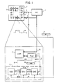
- FIG. 1 shows the array processor, which is similar in concept and operation to array processors known in the art, except insofar as handling of data dependencies and spatial dependencies is concerned.
- the image processor comprises adaptive processing element array 1 and array controller 2, both of which are shown schematically.
- Array controller 2 provides a set of instructions on instruction line 3, and provides a communication path 4 for input and output data.
- Processing element array 1 contains a great number of individual adaptive processing elements 5, each of which is equipped for adaptation according to this invention.
- Processing element array 1 might contain conventional processing elements 6, so long as there is awareness of which type of processing element is in each location, and housekeeping is done accordingly, but this is not preferred. It is preferred to make all the processing elements identical adaptive processing elements, and where conventional performance is desired, to adapt those elements, for example, those identified as elements 6, to perform conventionally.
- Image processing proceeds in conventional image processor fashion so far as dataflow is concerned; data enter the processing element array and flow from processing element to processing element in accordance with initial data values as modified by processing elements through which the data pass, without intervening access to system memory.
- the individual processing elements are set up prior to dataflow commencement.
- an image processor once set up, is for the duration of the execution a specialized, fixed operation computer.
- This invention provides for dynamic changes of setup during execution, by equipping each of the multiplicity of adaptable adaptive processing elements with its own processor identification register, its own data dependent status register, and its own instruction adaptation mechanism which is responsive to the composite of processor identification data, status data, and the applied instruction to provide internal selection of operation for the adaptive processing element.
- processor identification register e.g., a register for storing processor identification data, status data, and the applied instruction to provide internal selection of operation for the adaptive processing element.
- a representative one of the many adaptive processing elements 5, adaptive processing element 7, is shown in greater detail.
- Communication path 70, local memory 71, and arithmetic and logic unit (ALU) 72 are conventional, similar in scope and effect to the analogous items in a conventional processing element. In general, these items can function to accept an assignment (instruction) and execute the assignment on each item of data as it is presented.
- the computation cycle shown simplified in time line 8 uses an original instruction, shown simplified in original instruction view 9, to derive an instruction for execution.
- the original instruction, spatial dependent status and data dependent status values are available early in a cycle, as shown by values X,Y,Z on time line 8.
- the derived instruction then becomes available for control of computation C.
- Adaptability is provided by instruction adapter (IA) 73, which accepts from original instruction line 74 an instruction invoking adaptability, performs appropriate tests on data as presented, determines from test results whether to adapt by deriving a substitute instruction, and provides the substitute derived instruction to ALU 72 on derived instruction line 75.
- the ALU includes or serves as a data dependent status register to provide freshly processed data dependent status bits back on DDS test data line 76 to IA 73.
- the adaptability invoking instruction, presented on adaptability control line 74 is made available to spatial dependent status block (SDS) 77, to dependence select and verify block (DSV) 78, and to instruction modify and extend block (IME) 79.
- SDS spatial dependent status block
- DSV dependence select and verify block
- IME instruction modify and extend block
- the instruction adapter (IA) block 73 accepts an original instruction (of the type which invokes its own modification under specified circumstances) and generates, as output, a derived instruction on line 75 to ALU block 72. This controls the operations of the adaptive processing element.
- a typical instruction set such as that shown in NCR45CG72, 1984, at page 7, includes a micro-NOP instruction, several load/store instructions for inter-processing-element communication, and arithmetic/logic operations.
- FIG. 1 illustrates the instruction format of the derived instruction at inset derived instruction view 80.
- the derived instruction has an "agreement bit" inserted to the input instruction in one or more prescribed bit positions.
- the "agreement bit” is a function of the PID, DDS and the input instruction while the "prescribed bit position" can be predetermined from the format of the input instruction and the derived instruction.
- the "agreement bit” can also overwrite the bits of the input instruction at the prescribed positions.
- the individual adaptive processing element remains quite simple.
- Three major building blocks are registers, shift registers and multiplexers, all of which are common parts available from a number of suppliers and familiar to those skilled in the art. Such parts are described in THE TTL DATA BOOK FOR DESIGN ENGINEERS, Second Edition, Texas Instruments Corporation, LCC4112 74062-116-AI, pp. 7-471;7-316; and 7-181.
- the following examples are typical of building blocks appropriate for selection:
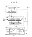
- FIG. 2 shows the structure of the instruction adapter (IA) 73, which contains three functional blocks as follows:
- the Spatial Dependence Status (SDS) block 77 accepts part of the input instruction as control and produces SDS bits as output to indicate the spatial dependence.
- This block contains a PID register 81 whose content is the PID of the PE.
- the PID register can be preloaded by the input instruction.
- the content of the PID register 81 must be correlated to spatial location, for example x-y coordinates.
- It also contains a shift register 82 of the same size as PID register 81.
- the shift register 82 can perform a logic-shift operation, one bit at a time, in either direction. This mechanism allows for any bit group of the PID register to be available on line 88 as the input to the DSV block 78.
- the second functional block is the "Dependence Select and Verify (DSV)" block 78.
- the DSV block 78 contains a multiplexer 83 to select some of the SDS bits or DDS bits.
- a template register 84 is included in this block for matching, masking and comparing purpose. The selected dependent bits and the template are passed to the "agreement verifier" 85 to generate an "agreement bit.”
- Template register 84 contains decision threshold information, preset at initialization. In a typical operation, all template registers are set to the same value to mask a certain subgroup of bits. On a particular cycle, all shift registers are operated similarly, according to instruction, to accomplish sampling of a group of bits in the related PID register and align those bits appropriately.
- the template register and shift register together function so as to select the interested bits from the PID.
- the usual operation is as a movable window, including two consecutive bits to assign the hardware differently for different items of interest or different image subsets.
- the agreement verifier can perform COMPARE, AND, OR and XOR operations.
- the DSV block accepts SDS bits and DDS bits as input, and generates the "agreement bit" as output.
- the DSV block accepts part of the input instruction as control.
- the DDS bits indicate the nature of the data and are used for data adaptation. Common DDS bits include positive/negative, zero/non-zero, positive/non-positive, true/false, greater/equal/less, even/odd. Any other status that can be derived from the Arithmetic Logic Unit (ALU) 72 of the adaptable processing element 7 can be identified by status bits.
- ALU Arithmetic Logic Unit
- the third block is the "instruction modify and extend (IME)" block 79.
- the IME block 79 accepts the agreement bit and the input instruction as inputs, and generates the derived instruction as output.
- the IME block 79 has a "bit overwriter” to replace some bits of the input instruction by the agreement bit at the prescribed positions.
- the block also has a "bit inserter” which inserts the agreement bit into the input instruction at the prescribed positions. The selection of overwriting or insertion or both, and the prescribing of the positions, are controlled by part of the input instruction.
- the IA can perform the following "dependent operations" to facilitate the spatial and/or data adaptation:
- FIG. 3 A very efficient simplified implementation of the Instruction Adaptor (IA) 73 is illustrated in Figure 3.
- the content of the PID register 81 is copied to a logical shift register (LSR) 91 which can perform logic-shift operations in both directions.
- the bits shifted out from them and the rightmost bit of the logical shift-register 91 are the SDS bits.
- a multiplexer then selects one of the SDS or DDS bit as the agreement bit.
- Such an implementation can perform one dimensional and two dimensional operations.
- This implementation is suitable for an adaptive processing element with less complexity, because of the elimination of the template register 84 (FIG. 2) and the agreement verifier 85.
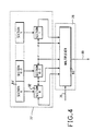
- FIG. 4 shows the spatial dependent status block generalized to detect spatial dependence of a multidimensional interconnection network of a parallel computer, such as an array in 2D or a pyramid in 3D.
- the PID register may be considered as comprising K sections 1-K.
- the shift register 92 which is analogous to the shift registers 82 and 91 in FIGs. 1-2, in SDS block 77, is partitioned into K sections, where K is the dimension of the network.
- Each section manipulates the spatial dependence for one dimension of the network.
- the rightmost and the leftmost bits of each section are SDS bits which are passed to the multiplexer 83 in the DSV block 78 for spatial dependence detection.
- Complementary operations are possible.
- An example of the complementary operation is the +/- (add or subtract) pair.
- the "agreement” bit is derived from the "condition,” which can be data-dependent or spatial-dependent.
- the sequential execution of action 1/action 2 can be totally parallelized into one unified action 3.
- the problem can also be restructured in the following way: An "agreement” bit is derived from the “condition” and is used to generate an "address offset” by either overwriting or inserting the appropriate field of the input instruction.
- the code for action 1 and action 2 are then structured D distance apart where D is equal to the "address offset.”
- each PE will"jump" to the right entry of the code according to the spatial condition of the data. Note that only one version of the coding is necessary.
- a non-homogeneous problem due to the spatial dependence can be converted to a homogeneous one by this invention, so that the degree of parallelism can be more extensive and software effort can be reduced.
- This invention resolves the spatial dependence due to the relative or absolute position (or coordinate) of PEs in a parallel computer which has one single fixed baseline network to connect the PEs in the system.
- the pyramid network can be emulated from the baseline array interconnection of size NxN by the adaptive instruction processor.
- the PID register of each adaptive processing element in the array is loaded with the appropriate Cartesian coordinate value (x, y).
- all PEs are active.
- only adaptive processing elements with x or y equals to the multiple of 2 are active.
- only adaptive processing elements with x or y equals to the multiple of 4 are active.
- at t i only adaptive processing elements with x or y equals to the multiple of 2x(i-1) are active.
- the above-described procedure emulates a pyramid network of shrinkage 2 (i.e.
- the same adaptive instruction processor can also be applied to the emulation of networks such as tree, ring and perfect shuffle etc. from a baseline interconnection.
- the network emulation is a very powerful mechanism in producing multiple parallel architectures from a single PE type. Along with the economic and logistic benefits, the algorithm can have a better match to the architecture, so that the performance can be increased. Because only one element type is required, such emulation scheme is especially suitable for VLSI implementation.
- a complementary operation is a pair of operations that can be distributed between two adaptive processing elements and executed simultaneously.
- Examples of the complementary operations include the SEND/RECEIVE pair for interprocessor communication and the Butterfly computation of FFT (Fast Fourier Transform).
- Another example is the +/- instruction described in application (1).
- the adaptive instruction scheme can speed the execution and save communication bandwidth.
- One adaptive processing element (based on the knowledge of its position in the array, i.e., spatial knowledge) sends data through an interconnection to its neighbor PE while its neighbor PE (based on this spatial knowledge) receives these data through the same interconnection.
- the operation can be accomplished in one cycle using one unit of communication bandwidth for one datum.
- the same operation needs two execution cycles and/or two units of communication bandwidth.
- Adaptive instruction processing can resolve the data dependent problem and increase the performance of a supercomputer.
- An instruction called OPA/OPB (operation A or operation B) can be defined and one agreement bit selected to adapt the instruction.
- the derived instruction will execute OPA if the agreement bit is "1" or OPB if the agreement bit is "0.”
- the pipe within the supercomputers can be set up in advance for instruction OPA/OPB and the vector execution can be started once the agreement bit is available. The probability of"guessing right"is always"1"because of the data adaptation.
- This example illustrates the adaptive instruction processor operating in a spatial adaptation case.
- this example shows how an original instruction is modified as a function of the Processor IDentification (PID).
- PID Processor IDentification
- the derived instruction has two bits, the r-th and the r+1-th bit, pertinent to this example.
- the action of the adaptive processing element is prescribed as follows:
- the PE performs "+" when the r-th bit of the modified instruction is "0" and the r+1-th bit is "1.”
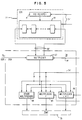
- Figure 5 shows another embodiment using multiple multiplexers.
- a portion of the original instruction commands the shift register 91, which contains the processor identification PID, to SHIFT RIGHT one bit position; as a result, the least significant bit in the processor identifiction register (LSBPID) is placed in one of the inputs to the Dependence Selection and Verify (DSV) Block 78.
- LSBPID least significant bit in the processor identifiction register
- Figure 5 illustrates a sample design to translate the K-th bit (I ⁇ K>) of the original instruction into the r-th and the r+1-th bits (IM ⁇ r> and IM ⁇ r+1>) of the modified instruction according to the Least Significant Bit of PID (LSBPID, i.e. PID ⁇ 0>).
- LSBPID Least Significant Bit of PID
- the "agreement bit" (now carrying the LSBPID) and the original instruction (carrying I ⁇ K> and other bits) are routed into a set of multiplexers 84-86 to produce the derived instruction.
- J multiplexers are required for a J-bit derived instruction, one multiplexer to produce one bit of the derived instruction.
- the original instruction command the "multiplexer r" to SELECT I ⁇ K> as the output.
- the original instruction commands "multiplexer r+1" to SELECT the "agreement bit" as IM ⁇ r+1>.
- a table below shows the relationship among the original instruction (I ⁇ K>), the LSBPID and the modified instruction (IM ⁇ r> and IM ⁇ r+1>), which demonstrates the realization of the invention via the design illustrated in Figure 5.
Abstract
Description
- This invention relates to image processors which process data streams passing through arrays of processing elements, each processing element executing an assigned instruction, and more particularly relates to an architecture for adaptively manipulating the instruction assignment of each processing element in response to spatial and data values in the data stream, using an instruction adapter, individual to each processing element, to derive a new instruction as a composite function of processor identification and status and of the data stream.
- The following publications are representative of the prior art:
- United States Patent 3,287,702; Borck, Jr., et al, COMPUTER CONTROL, Nov. 22, 1966, shows an array processor with computer control of an array of conventional processing elements.
- United States Patent 3,287,703; D.L. Slotnick, COMPUTER, Nov. 22, 1966 shows a similar array processor.
- United States Patent 3,970,993, C.A. Finnila, COOPERATIVE-WORD LINEAR ARRAY PARALLEL PROCESSOR, July 20, l976 shows an array processor in which each processing element includes a flag register which can modify the operations on the common control lines.
- United States Patent 4,187,539, J.R. Eaton, PIPELINED DATA PROCESSING SYSTEM WITH CENTRALIZED MICROPROGRAM CONTROL, Feb. 5, l980 shows a plural dataflow pipelined processor in which each dataflow includes a shift register which provides a sequence of microinstructions, and a common microprogram control unit includes a flag register which helps keep the instruction size small by providing instruction information which does not change often.
- United States Patent 4,287,566, G.J. Culler, ARRAY PROCESSOR WITH PARALLEL OPERATIONS PER INSTRUCTION, Sept. 01, 1981, shows an array processor having subarrays used to calculate vector addresses.
- United States Patent 4,344,134, G.H. Barnes, PARTITIONABLE PARALLEL PROCESSOR, August 10, l982, shows a partitionable array processor in which each processor in a node tree issues a ready signal when the dataflow has passed it, thus invoking the next instruction.
- United States Patent 4,380,046, L-W. Fung, MASSIVELY PARALLEL PROCESSOR COMPUTER, April 12, l983, shows an array processor with each processing element equipped with a mask bit register, identified as G-register, to disable the processing element and thus distinguished between executing the current instruction or no-operation; that is, each processing element has a G-register with an OP/NOP flag.
- United States Patent 4,467,409, Potash et al, FLEXIBLE COMPUTER ARCHITECTURE USING ARRAYS OF STANDARDIZED MICROPROCESSORS CUSTOMIZED FOR PIPELINE AND PARALLEL OPERATIONS, August 21, 1984, shows a flexible architecture for a sequential processor, using standardized units with "soft functional structures" which customize a unit for a command. The units thus can be manufactured as standard units and customized by means of a mask which sets contacts in the soft functional structure.
- United States Patent 4,558,411, Farber et al, POLYMORPHIC PROGRAMMABLE UNITS EMPLOYING PLURAL LEVELS OF SUB-INSTRUCTION SETS, December 10, 1985, shows a multiple-level programmable unit to provide a hierarchy of sub-instruction sets of microprogramming, to change, for example, from input output mode to processing mode or to execute programs written in differing languages.
- European Patent Application Number 84301600.7, Holsztynski, DATA PROCESSING CELLS AND PARALLEL DATA PROCESSORS INCORPORATING SUCH CELLS, October 17, 1984, shows an array processor in which each processing element includes a full adder and storage devices for N-S (north-south), E-W (east-west), and C (carry), so that the processing element can carry out both arithmetic and logic functions.
- U.S.S.R. Author's Certificate Number 83-721416/30, ASSOCIATIVE PROCESSORS MICROPROGRAM CONTROL APPARATUS, Tbilisi Elva Combine, September 15, 1982, shows first and second control instruction registers in instruction memory to allow the same microinstruction to be used for different instructions, reducing the overall volume of memory.
- Davis et al, SYSTOLIC ARRAY CHIP MATCHES THE PACE OF HIGH-SPEED PROCESSING, Electronic Design, October 31, 1984, pp 207-218, shows a representative array processor.
- NCR GEOMETRIC ARITHMETIC PARALLEL PROCESSOR, product specification NCR45CG72, NCR Corp., Dayton, OH, 1984, pp. 1-12, shows physical characteristics of a representative array processor.
- Cloud et al, HIGHER EFFICIENCY FOR PARALLEL PROCESSORS, IEEE Southcon, reprint published by NCR Corporation Micro electronics Div., Fort Collins, CO, pp. 1-7, shows details of operation of NCR's geometric arithmetic parallel processor (GAPP).
- The prior art shows a variety of array processors, with individual processing elements controllable externally in a variety of manners, and with the possibility of OP/NOP according to a flag in the individual processing element-- but the prior art does not teach the use of instruction adaptation within each individual adaptive processing element to make an array processor dynamically optimizable to spatial and data dependencies through derived instruction within the adaptive processing element.
- Current computer systems are categorized, according to instruction stream and data stream, into four classes. They are:
· SISD (Single Instruction stream Single Data stream).
· SIMD (Single Instruction stream Multiple Data stream).
· MISD (Multiple Instruction stream Single Data stream).
· MIMD (Multiple Instruction stream Multiple Data stream).
Except for SISD, these architectures are parallel processing systems. However, none of them can perform parallel operations which are adaptive to the spatial condition of a processing element (spatial adaptations, e.g. data are at the border of an image or the processing element is at the first column of an array). Neither can they perform parallel operations adaptive to the nature of the data (data adaptation, e.g. data positive / data negative; flag true / flag false). - Supercomputers are commercially available now and exemplified by the Cyber series from CDC, the CRAY series from CRAY Research and the NEC AP series. All these machines are of MISD architecture and require a long setup time for setting up the instruction pipe to process a vector. The overhead is large if the frequency of the pipe setup is high or the vector is short; the performance is consequently low in such cases.
- Data dependence in a loop degrades the performance of these supercomputers. The machines are either prevented from presetting the pipe until the date dependence is resolved (e.g. status is known exactly) or will set up the pipe for one path (e.g., status is true) with higher probability. The former case delays the execution while the latter case involves the resetting of the pipe (i.e. increase the pipe setup frequency) if the "guess" is wrong. Both cases degrade the performance.
- The lack of spatial and/or data adaptation leads to the following drawbacks:
- 1. Data-dependent operations are processed sequentially, which leads to a waste of the parallel hardware, hence to lower performance;
- 2. Data with spatial significance are treated as exception, which prevent the parallel opportunity;
- 3. Interconnections of parallel computers are fixed, which restricts the algorithm versatility;
- 4. Complementary operations (e.g. SEND/RECEIVE pair) caused by data or spatial dependence are performed sequentially, which implies longer execution time;
- 5. Communication bandwidth is accordingly wasted;
- 6. Different copies of the program must be generated for processing elements (PEs) with different spatial conditions, which leads to larger software effort.
- The prior art does not teach nor suggest the invention, which provides for instruction adaptation at the processing element level for spatial and data dependencies, by providing each of a finite number of processing elements with conditional instruction modification means.
- To facilitate a quick understanding of the invention, it is helpful to describe the situations where data-dependent parallel processing and spatial- dependent parallel processing are involved, and where improved solutions, such as by means of the invention, are most desirable.
- With adaptive instruction processing, the above problem could be handled in a parallel fashion as follows:
An instruction is defined as +/- (add or subtract) while, using the "status" as the "agreement bit," the derived instruction is defined as + (add) if the "status" is true, or is defined as - (subtract) if the "status" is false. The loop with data dependence can then be rewritten as
for (i=0; i<300; i++)
for (j=0; j<500; j++)
c[i,j]=a[i,j]+/-b[i,j];
and parallel processing can be applied efficiently. - This example demonstrates one instance of how data dependence can be resolved, and how the data dependent loops that were processed sequentially can now be parallelized. The opportunity of exploiting the parallelism that involves data dependence is not limited to the above example and is much wider in application.
- Current parallel computers are efficient in processing a loop with a long running index, but do not support efficiently the loop with data dependence. Specifically, one type of data independent loop is shown as follows:
for (i=0; i<300; i++)
for (j=0; j<500; j++)
c[i,j]=a[i,j]+b[i,j];
The processing can be very well supported by most known SIMD, MISD and MIMD machines. - But when the data dependence is added to the program as shown in the following, no existing parallel machines can handle it efficiently.
for (i=0; i<300; i++)
for (j=0; j<500; j++)
if (status)
c[i,j]=a[i,j]+b[i,j];
else
c[i,j]=a[i,j]-b[i,j]; - In image processing and other applications where data are associated with spatial conditions, data are not handled homogeneously, but rather are subject to their spatial dependence. For example, the data on the boundary of an image are treated differently from the other non-boundary data; this is one type of spatial dependence reflected by data. In this situation, there are two major drawbacks when applying parallel processing:
- 1. The degree of parallelism can only be extended to the homogeneous part of the data; consequently, the non-homogeneous data (e.g. boundary) are forced to be processed sequentially. This degrades the performance of a parallel system;
- 2. The program (or coding) for the non-homogeneous data differs from the program for their homogeneous counterpart; therefore, more than one copy of the coding must be prepared. This leads to larger software effort.
- If the instruction could be adapted, processing with the spatial dependence could solve problems such as the above problem as follows:
for(i=0; i<300; i++)
for (j=0; j<500; j++)
if (spatial-condition)
action 1;
then
action 2. - With adaptive instruction processing, both drawbacks could be removed. The spatial condition for the non-homogeneity, for example the boundary, could be expressed as conditions such as x<B or x>N-B or y<B or y>N-B, where (x,y) is the coordinate of a pixel of an NxN image and B is the width of the boundary.
- The object of the invention is to provide an image processor architecture which speeds the operation of the image processing system by eliminating delays related to spatial or data dependence.
- A feature of the invention is the provision, in each of a finite number of processing elements, of an instruction adapter with addressable instruction derivation means, responsive to the composite of original instruction and bit values in the data stream.
- An advantage of the invention is that the image processing system is self-adaptive to the parameters of the data stream, in that an individual processing element may derive different instructions adapted to the spatial or data parameters of different items as the items arrive for processing at the individual processing element.
- Another advantage of the invention is that is does not require processing delay time for data dependencies.
- The foregoing and other objects, features and advantages of the invention will be apparent from the more particular description of the preferred embodiments of the invention, as illustrated in the accompanying drawings.
-
- FIG. 1 is a block diagram of an array processor with one representative adaptive processing element present in block diagram according to the invention.
- FIG. 2 is a detailed block diagram of the instruction adapter IA of FIG. 1.
- FIG. 3 is a detailed block diagram of an instruction adapter according to a simplified embodiment.
- FIG. 4 is a detailed block diagram of an instruction adapter for a multidimensional network array processor.
- FIG. 5 is a detailed block diagram of a further embodiment of the instruction adapter.
- The adaptive instruction processor assigns a processor identification (PID) to each adaptive processing element in the parallel computer. It collects a set of data-dependent-status (DDS) bits from the arithmetic & logic unit (ALU) of the adaptive processing element. It then uses an Instruction Adapter (IA) to derive the instruction subject to the spatial dependence and data dependence reflected by the PID, DDS and the original instruction.
- FIG. 1 shows the array processor, which is similar in concept and operation to array processors known in the art, except insofar as handling of data dependencies and spatial dependencies is concerned. The image processor comprises adaptive
processing element array 1 andarray controller 2, both of which are shown schematically.Array controller 2 provides a set of instructions oninstruction line 3, and provides acommunication path 4 for input and output data.Processing element array 1 contains a great number of individual adaptive processing elements 5, each of which is equipped for adaptation according to this invention.Processing element array 1 might contain conventional processing elements 6, so long as there is awareness of which type of processing element is in each location, and housekeeping is done accordingly, but this is not preferred. It is preferred to make all the processing elements identical adaptive processing elements, and where conventional performance is desired, to adapt those elements, for example, those identified as elements 6, to perform conventionally. - Image processing proceeds in conventional image processor fashion so far as dataflow is concerned; data enter the processing element array and flow from processing element to processing element in accordance with initial data values as modified by processing elements through which the data pass, without intervening access to system memory. The individual processing elements are set up prior to dataflow commencement. In a conventional image processor, there is little chance to alter the setup during execution because for all practical purposes the exact position of data during execution is unknown. In essence, an image processor, once set up, is for the duration of the execution a specialized, fixed operation computer. This invention provides for dynamic changes of setup during execution, by equipping each of the multiplicity of adaptable adaptive processing elements with its own processor identification register, its own data dependent status register, and its own instruction adaptation mechanism which is responsive to the composite of processor identification data, status data, and the applied instruction to provide internal selection of operation for the adaptive processing element. On a system ba sis, this provides convenient adaptation to spatial and data dependencies, which permits system optimization for the type of data being processed.
- A representative one of the many adaptive processing elements 5,
adaptive processing element 7, is shown in greater detail.Communication path 70,local memory 71, and arithmetic and logic unit (ALU) 72 are conventional, similar in scope and effect to the analogous items in a conventional processing element. In general, these items can function to accept an assignment (instruction) and execute the assignment on each item of data as it is presented. - The computation cycle, shown simplified in time line 8, uses an original instruction, shown simplified in
original instruction view 9, to derive an instruction for execution. In operation, the original instruction, spatial dependent status and data dependent status values are available early in a cycle, as shown by values X,Y,Z on time line 8. The derived instruction then becomes available for control of computation C. - Adaptability is provided by instruction adapter (IA) 73, which accepts from
original instruction line 74 an instruction invoking adaptability, performs appropriate tests on data as presented, determines from test results whether to adapt by deriving a substitute instruction, and provides the substitute derived instruction to ALU 72 on derivedinstruction line 75. The ALU includes or serves as a data dependent status register to provide freshly processed data dependent status bits back on DDS test data line 76 toIA 73. The adaptability invoking instruction, presented onadaptability control line 74, is made available to spatial dependent status block (SDS) 77, to dependence select and verify block (DSV) 78, and to instruction modify and extend block (IME) 79. The instruction adapter (IA)block 73 accepts an original instruction (of the type which invokes its own modification under specified circumstances) and generates, as output, a derived instruction online 75 toALU block 72. This controls the operations of the adaptive processing element. - A typical instruction set, such as that shown in NCR45CG72, 1984, at
page 7, includes a micro-NOP instruction, several load/store instructions for inter-processing-element communication, and arithmetic/logic operations. FIG. 1 illustrates the instruction format of the derived instruction at inset derivedinstruction view 80. The derived instruction has an "agreement bit" inserted to the input instruction in one or more prescribed bit positions. The "agreement bit" is a function of the PID, DDS and the input instruction while the "prescribed bit position" can be predetermined from the format of the input instruction and the derived instruction. The "agreement bit" can also overwrite the bits of the input instruction at the prescribed positions. - The individual adaptive processing element remains quite simple. Three major building blocks are registers, shift registers and multiplexers, all of which are common parts available from a number of suppliers and familiar to those skilled in the art. Such parts are described in THE TTL DATA BOOK FOR DESIGN ENGINEERS, Second Edition, Texas Instruments Corporation, LCC4112 74062-116-AI, pp. 7-471;7-316; and 7-181. The following examples are typical of building blocks appropriate for selection:

- FIG. 2 shows the structure of the instruction adapter (IA) 73, which contains three functional blocks as follows:
- 1. Spatial dependent status block (SDS) 77;
- 2. Dependence select and verify block (DSV) 78; and
- 3. Instruction modify and extend block (B) 79.
- The Spatial Dependence Status (SDS)
block 77 accepts part of the input instruction as control and produces SDS bits as output to indicate the spatial dependence. This block contains aPID register 81 whose content is the PID of the PE. The PID register can be preloaded by the input instruction. The content of thePID register 81 must be correlated to spatial location, for example x-y coordinates. It also contains ashift register 82 of the same size asPID register 81. Theshift register 82 can perform a logic-shift operation, one bit at a time, in either direction. This mechanism allows for any bit group of the PID register to be available online 88 as the input to theDSV block 78. - The second functional block is the "Dependence Select and Verify (DSV)"
block 78. TheDSV block 78 contains amultiplexer 83 to select some of the SDS bits or DDS bits. Atemplate register 84 is included in this block for matching, masking and comparing purpose. The selected dependent bits and the template are passed to the "agreement verifier" 85 to generate an "agreement bit."Template register 84 contains decision threshold information, preset at initialization. In a typical operation, all template registers are set to the same value to mask a certain subgroup of bits. On a particular cycle, all shift registers are operated similarly, according to instruction, to accomplish sampling of a group of bits in the related PID register and align those bits appropriately. - The template register and shift register together function so as to select the interested bits from the PID.
- The usual operation is as a movable window, including two consecutive bits to assign the hardware differently for different items of interest or different image subsets.
- The agreement verifier can perform COMPARE, AND, OR and XOR operations. In summary, the DSV block accepts SDS bits and DDS bits as input, and generates the "agreement bit" as output. The DSV block accepts part of the input instruction as control.
- The DDS bits indicate the nature of the data and are used for data adaptation. Common DDS bits include positive/negative, zero/non-zero, positive/non-positive, true/false, greater/equal/less, even/odd. Any other status that can be derived from the Arithmetic Logic Unit (ALU) 72 of the
adaptable processing element 7 can be identified by status bits. - The third block is the "instruction modify and extend (IME)"
block 79. TheIME block 79 accepts the agreement bit and the input instruction as inputs, and generates the derived instruction as output. TheIME block 79 has a "bit overwriter" to replace some bits of the input instruction by the agreement bit at the prescribed positions. The block also has a "bit inserter" which inserts the agreement bit into the input instruction at the prescribed positions. The selection of overwriting or insertion or both, and the prescribing of the positions, are controlled by part of the input instruction. - With these three functional blocks, the IA can perform the following "dependent operations" to facilitate the spatial and/or data adaptation:
- (1) detecting any one bit of DDS being "1";
- (2) detecting the i-th bit of the PID register being "1"; and
- (3) detecting any M contiguous bits of the PID register matching to the template where M is smaller or equal to the total number of bits of the PID.
- The above-described generic embodiment encompasses the invention. Specific implementations can be a partial collection of each functional block.
- A very efficient simplified implementation of the Instruction Adaptor (IA) 73 is illustrated in Figure 3. The content of the
PID register 81 is copied to a logical shift register (LSR) 91 which can perform logic-shift operations in both directions. The bits shifted out from them and the rightmost bit of the logical shift-register 91 are the SDS bits. A multiplexer then selects one of the SDS or DDS bit as the agreement bit. Such an implementation can perform one dimensional and two dimensional operations. This implementation is suitable for an adaptive processing element with less complexity, because of the elimination of the template register 84 (FIG. 2) and theagreement verifier 85. - FIG. 4 shows the spatial dependent status block generalized to detect spatial dependence of a multidimensional interconnection network of a parallel computer, such as an array in 2D or a pyramid in 3D. The PID register may be considered as comprising K sections 1-K. The
shift register 92, which is analogous to the shift registers 82 and 91 in FIGs. 1-2, inSDS block 77, is partitioned into K sections, where K is the dimension of the network. Each section manipulates the spatial dependence for one dimension of the network. The rightmost and the leftmost bits of each section are SDS bits which are passed to themultiplexer 83 in theDSV block 78 for spatial dependence detection. -
- With adaptive instruction processing according to the invention, one can restructure as follows:
for (i=0; i<300; i++)
for (j=0; j<500; j++)
if (condition)
action 1;
else
action 2; (ifaction 1 andaction 2 are complementary)
into
for(i=0; i<300; i++)
for(j=0; j<500; j++)
action 3. - Complementary operations are possible. An example of the complementary operation is the +/- (add or subtract) pair. The "agreement" bit is derived from the "condition," which can be data-dependent or spatial-dependent. As the result of the restructuring, the sequential execution of
action 1/action 2 can be totally parallelized into oneunified action 3. - The problem can also be restructured in the following way:
An "agreement" bit is derived from the "condition" and is used to generate an "address offset" by either overwriting or inserting the appropriate field of the input instruction. The code foraction 1 andaction 2 are then structured D distance apart where D is equal to the "address offset." During the runtime, each PE will"jump" to the right entry of the code according to the spatial condition of the data. Note that only one version of the coding is necessary. A non-homogeneous problem due to the spatial dependence can be converted to a homogeneous one by this invention, so that the degree of parallelism can be more extensive and software effort can be reduced. - This invention resolves the spatial dependence due to the relative or absolute position (or coordinate) of PEs in a parallel computer which has one single fixed baseline network to connect the PEs in the system.
- It is advantageous from an algorithm development point of view to have more than one network (or interconnection) embedded in a parallel processing system, because no single network optimally matches to various algorithms. In a parallel system with such network emulation capability, a network can be emulated from the baseline interconnection via using the adaptive instruction processor.
- For example, the pyramid network can be emulated from the baseline array interconnection of size NxN by the adaptive instruction processor. The PID register of each adaptive processing element in the array is loaded with the appropriate Cartesian coordinate value (x, y). At time t=1, all PEs are active. At t=2, only adaptive processing elements with x or y equals to the multiple of 2 are active. At t=3, only adaptive processing elements with x or y equals to the multiple of 4 are active. In summary, at t=i only adaptive processing elements with x or y equals to the multiple of 2x(i-1) are active. The above-described procedure emulates a pyramid network of shrinkage 2 (i.e. for every further time step, only 1/4 of the total PEs are connected with distance one) from the baseline array network. The control of the emulation can be done by examining the content of the two-dimensional PID register and activates the PE if the "agreement" bit is true.
- The same adaptive instruction processor can also be applied to the emulation of networks such as tree, ring and perfect shuffle etc. from a baseline interconnection.
- The network emulation is a very powerful mechanism in producing multiple parallel architectures from a single PE type. Along with the economic and logistic benefits, the algorithm can have a better match to the architecture, so that the performance can be increased. Because only one element type is required, such emulation scheme is especially suitable for VLSI implementation.
- A complementary operation is a pair of operations that can be distributed between two adaptive processing elements and executed simultaneously. Examples of the complementary operations include the SEND/RECEIVE pair for interprocessor communication and the Butterfly computation of FFT (Fast Fourier Transform). Another example is the +/- instruction described in application (1). When applied to the complementary operations, the adaptive instruction scheme can speed the execution and save communication bandwidth.
- Consider the SEND/RECEIVE example for the SIMD array architecture. One adaptive processing element (based on the knowledge of its position in the array, i.e., spatial knowledge) sends data through an interconnection to its neighbor PE while its neighbor PE (based on this spatial knowledge) receives these data through the same interconnection. The operation can be accomplished in one cycle using one unit of communication bandwidth for one datum. For the SIMD architecture without topology-dependent adaptation, the same operation needs two execution cycles and/or two units of communication bandwidth.
- In the case of Butterfly computation, sequential execution in a conventional image processor may require 4 cycles. With the adaptive instruction processor, it can be reduced to 2 cycles, (with 2 adaptive processing elements) or even to 1 cycle (with 4 adaptive processing elements). This is achieved by first sending the instruction ADD/SUB to all adaptive processing elements. Each adaptive processing element then maps the instruction into either ADD or SUB according to its spatial condition.
- Application of complementary operations are not limited to the above examples. In fact, many other applications can be found in image processing, computer vision, digital signal processing, mathematical transformation and general scientific computation.
- Adaptive instruction processing can resolve the data dependent problem and increase the performance of a supercomputer. An instruction called OPA/OPB (operation A or operation B) can be defined and one agreement bit selected to adapt the instruction. The derived instruction will execute OPA if the agreement bit is "1" or OPB if the agreement bit is "0." The pipe within the supercomputers can be set up in advance for instruction OPA/OPB and the vector execution can be started once the agreement bit is available. The probability of"guessing right"is always"1"because of the data adaptation.
- This example illustrates the adaptive instruction processor operating in a spatial adaptation case. With the aid of Figure 5, this example shows how an original instruction is modified as a function of the Processor IDentification (PID). As a result, the following computation
for (i=0; i<300; i++)
for (j=0; j<500; j++)
if (PID<0> == 1)
c[i,j] = a[i,j] + b[i,j]
else
c[i,j] = a[i,j] - b[i,j]
can be executed efficiently. - A simplified original instruction and derived instructions are depicted first as a background; then a design realizing the invention is detailed in Figure 5 with companion description.
- Among the M bits of the original instruction, the K-th bit controls the action of either SEND/REC or +/- as described below:
If bit<K>=1, then PE performs SEND when the PE's local status S is true;
PE performs REC when the PE's local status S is false;
If bit<K>=0, then PE performs "+" when PE's local status S is true;
PE performs "-" when the PE's local status S is false. - In contrast to the original instruction, the derived instruction has two bits, the r-th and the r+1-th bit, pertinent to this example. The action of the adaptive processing element is prescribed as follows:

- For instance, the PE performs "+" when the r-th bit of the modified instruction is "0" and the r+1-th bit is "1."
- Figure 5 shows another embodiment using multiple multiplexers. A portion of the original instruction commands the
shift register 91, which contains the processor identification PID, to SHIFT RIGHT one bit position; as a result, the least significant bit in the processor identifiction register (LSBPID) is placed in one of the inputs to the Dependence Selection and Verify (DSV)Block 78. - Figure 5 illustrates a sample design to translate the K-th bit (I<K>) of the original instruction into the r-th and the r+1-th bits (IM<r> and IM<r+1>) of the modified instruction according to the Least Significant Bit of PID (LSBPID, i.e. PID<0>).
- Another portion of the original instruction on adaptability control lines 74ʹ then commands the
DSV block 78 to SELECT the LSBPID as the output of the multiplexer in DSV Block. Consequently, LSBPID is placed on the line of "agreement bit." - As the inputs of the Instruction Modify and Extend (IME)
Block 79, the "agreement bit" (now carrying the LSBPID) and the original instruction (carrying I<K> and other bits) are routed into a set of multiplexers 84-86 to produce the derived instruction. J multiplexers are required for a J-bit derived instruction, one multiplexer to produce one bit of the derived instruction. To produce IM<r>, the original instruction command the "multiplexer r" to SELECT I<K> as the output. Similarly, the original instruction commands "multiplexer r+1" to SELECT the "agreement bit" as IM<r+1>. - A table below shows the relationship among the original instruction (I<K>), the LSBPID and the modified instruction (IM<r> and IM<r+1>), which demonstrates the realization of the invention via the design illustrated in Figure 5.

- Thus, while the invention has been described with reference to a preferred embodiment, it will be understood by those skilled in the art that various changes in form and details may be made without departing from the scope of the invention.
Claims (6)
--characterized in that--
each of the processing elements is adaptive, in that each adaptive processing element derives an instruction and executes the derived instruction,
each adaptive processing element comprising:
means to derive an instruction as a composite function of applied instruction and dynamic operational parameters; and
means to execute said derived instruction.
--characterized in that--
each of the processing elements is adaptive, in that each adaptive processing element derives an instruction and executes the derived instruction,
each adaptive processing element comprising:
spatial dependent status means (77) to provide an indication of a spatial dependent status operational parameter at a first internal node;
execution means, including the processing means (72), to execute a derived instruction and to provide a result to the output means and also to provide a data dependent status operational parameter at a second internal node;
dependence select and verify means (78), connected to said first internal node and to said second internal node to derive an instruction as a composite function of applied instruction and dynamic operational parameters; and
instruction modification and extension means (79), connected to the instruction input node of the processing means, to supply a derived instruction to the processing means.
in which said processing means (72) comprises data dependent status register means (76); and
in which said instruction modification and extension means (79) is connected to said processing means (72) to provide processing activity which is a composite function of applied instruction and the current data content of said processor identification register and the current data content of said data dependent status register.
a processor identification register (81) and a shift register (82);
and wherein said dependence select and verify means (78) comprises a template register (84) and an agreement verifier (85),
whereby said processor identification register, said shift register and said agreement verifier serve as a movable window to provide bits for control of instruction derivation by the adaptive processing element.
a processor identification register (81ʹ) is divided into sections 1...K-1, K and said shift register means (92) is similarly divided into sections 1...K-1, K and interconnected section by section with said processor identification register (81ʹ).
Applications Claiming Priority (2)
| Application Number | Priority Date | Filing Date | Title |
|---|---|---|---|
| US839311 | 1986-03-13 | ||
| US06/839,311 US4783738A (en) | 1986-03-13 | 1986-03-13 | Adaptive instruction processing by array processor having processor identification and data dependent status registers in each processing element |
Publications (3)
| Publication Number | Publication Date |
|---|---|
| EP0237013A2 true EP0237013A2 (en) | 1987-09-16 |
| EP0237013A3 EP0237013A3 (en) | 1989-02-08 |
| EP0237013B1 EP0237013B1 (en) | 1993-02-10 |
Family
ID=25279392
Family Applications (1)
| Application Number | Title | Priority Date | Filing Date |
|---|---|---|---|
| EP87103374A Expired - Lifetime EP0237013B1 (en) | 1986-03-13 | 1987-03-10 | Adaptive instruction processing by array processor having processor identification and data dependent status registers in each processing element |
Country Status (5)
| Country | Link |
|---|---|
| US (1) | US4783738A (en) |
| EP (1) | EP0237013B1 (en) |
| JP (1) | JPH0719244B2 (en) |
| CA (1) | CA1268554A (en) |
| DE (1) | DE3784082T2 (en) |
Cited By (2)
| Publication number | Priority date | Publication date | Assignee | Title |
|---|---|---|---|---|
| EP0314277A2 (en) * | 1987-10-27 | 1989-05-03 | International Business Machines Corporation | Simd array processor |
| EP0724221A3 (en) * | 1995-01-26 | 1997-03-12 | Ibm | Method and apparatus for executing dissimilar seq. of instructions in the processor of a single-instruction-multiple data (SIMD) computer |
Families Citing this family (82)
| Publication number | Priority date | Publication date | Assignee | Title |
|---|---|---|---|---|
| DE3506749A1 (en) * | 1984-02-27 | 1985-09-26 | Nippon Telegraph & Telephone Public Corp., Tokio/Tokyo | Matrix processor and control method therefor |
| US4839851A (en) * | 1987-07-13 | 1989-06-13 | Idaho Research Foundation, Inc. | Programmable data path device |
| US4943912A (en) * | 1987-10-13 | 1990-07-24 | Hitachi, Ltd. | Parallel processor system having control processor and array control apparatus for selectively activating different processors |
| US4901360A (en) * | 1987-10-23 | 1990-02-13 | Hughes Aircraft Company | Gated architecture for computer vision machine |
| NL8800071A (en) * | 1988-01-13 | 1989-08-01 | Philips Nv | DATA PROCESSOR SYSTEM AND VIDEO PROCESSOR SYSTEM, PROVIDED WITH SUCH A DATA PROCESSOR SYSTEM. |
| US5257395A (en) * | 1988-05-13 | 1993-10-26 | International Business Machines Corporation | Methods and circuit for implementing and arbitrary graph on a polymorphic mesh |
| US5136717A (en) * | 1988-11-23 | 1992-08-04 | Flavors Technology Inc. | Realtime systolic, multiple-instruction, single-data parallel computer system |
| US5280620A (en) * | 1988-12-16 | 1994-01-18 | U.S. Philips Corporation | Coupling network for a data processor, including a series connection of a cross-bar switch and an array of silos |
| US5067069A (en) * | 1989-02-03 | 1991-11-19 | Digital Equipment Corporation | Control of multiple functional units with parallel operation in a microcoded execution unit |
| CA2012938A1 (en) * | 1989-04-19 | 1990-10-19 | Patrick F. Castelaz | Clustering and association processor |
| EP0424618A3 (en) * | 1989-10-24 | 1992-11-19 | International Business Machines Corporation | Input/output system |
| US5471593A (en) * | 1989-12-11 | 1995-11-28 | Branigin; Michael H. | Computer processor with an efficient means of executing many instructions simultaneously |
| JPH05506113A (en) * | 1990-01-05 | 1993-09-02 | マスパー・コンピューター・コーポレイション | parallel processor memory system |
| US5963745A (en) * | 1990-11-13 | 1999-10-05 | International Business Machines Corporation | APAP I/O programmable router |
| US5590345A (en) * | 1990-11-13 | 1996-12-31 | International Business Machines Corporation | Advanced parallel array processor(APAP) |
| US5794059A (en) * | 1990-11-13 | 1998-08-11 | International Business Machines Corporation | N-dimensional modified hypercube |
| US5765012A (en) * | 1990-11-13 | 1998-06-09 | International Business Machines Corporation | Controller for a SIMD/MIMD array having an instruction sequencer utilizing a canned routine library |
| US5966528A (en) * | 1990-11-13 | 1999-10-12 | International Business Machines Corporation | SIMD/MIMD array processor with vector processing |
| US5765015A (en) * | 1990-11-13 | 1998-06-09 | International Business Machines Corporation | Slide network for an array processor |
| US5630162A (en) * | 1990-11-13 | 1997-05-13 | International Business Machines Corporation | Array processor dotted communication network based on H-DOTs |
| US5625836A (en) * | 1990-11-13 | 1997-04-29 | International Business Machines Corporation | SIMD/MIMD processing memory element (PME) |
| ATE180586T1 (en) * | 1990-11-13 | 1999-06-15 | Ibm | PARALLEL ASSOCIATIVE PROCESSOR SYSTEM |
| US5734921A (en) * | 1990-11-13 | 1998-03-31 | International Business Machines Corporation | Advanced parallel array processor computer package |
| US5828894A (en) * | 1990-11-13 | 1998-10-27 | International Business Machines Corporation | Array processor having grouping of SIMD pickets |
| US5765011A (en) * | 1990-11-13 | 1998-06-09 | International Business Machines Corporation | Parallel processing system having a synchronous SIMD processing with processing elements emulating SIMD operation using individual instruction streams |
| US5588152A (en) * | 1990-11-13 | 1996-12-24 | International Business Machines Corporation | Advanced parallel processor including advanced support hardware |
| US5809292A (en) * | 1990-11-13 | 1998-09-15 | International Business Machines Corporation | Floating point for simid array machine |
| US5617577A (en) * | 1990-11-13 | 1997-04-01 | International Business Machines Corporation | Advanced parallel array processor I/O connection |
| US5815723A (en) * | 1990-11-13 | 1998-09-29 | International Business Machines Corporation | Picket autonomy on a SIMD machine |
| US5752067A (en) * | 1990-11-13 | 1998-05-12 | International Business Machines Corporation | Fully scalable parallel processing system having asynchronous SIMD processing |
| US5963746A (en) * | 1990-11-13 | 1999-10-05 | International Business Machines Corporation | Fully distributed processing memory element |
| US5594918A (en) * | 1991-05-13 | 1997-01-14 | International Business Machines Corporation | Parallel computer system providing multi-ported intelligent memory |
| US5237626A (en) * | 1991-09-12 | 1993-08-17 | International Business Machines Corporation | Universal image processing module |
| JP2571655B2 (en) * | 1991-11-27 | 1997-01-16 | インターナショナル・ビジネス・マシーンズ・コーポレイション | Protocol conversion mechanism, switching network and computer system |
| JPH06131312A (en) * | 1992-01-23 | 1994-05-13 | Hitachi Ltd | Method and system for parallel processing |
| JP2642039B2 (en) * | 1992-05-22 | 1997-08-20 | インターナショナル・ビジネス・マシーンズ・コーポレイション | Array processor |
| US5581778A (en) * | 1992-08-05 | 1996-12-03 | David Sarnoff Researach Center | Advanced massively parallel computer using a field of the instruction to selectively enable the profiling counter to increase its value in response to the system clock |
| US5579527A (en) * | 1992-08-05 | 1996-11-26 | David Sarnoff Research Center | Apparatus for alternately activating a multiplier and a match unit |
| US6298162B1 (en) | 1992-12-23 | 2001-10-02 | Lockheed Martin Corporation | Image compression/expansion using parallel decomposition/recomposition |
| US5493651A (en) * | 1993-02-16 | 1996-02-20 | International Business Machines Corporation | Method and system for dequeuing connection requests in a simplex switch |
| JP3287901B2 (en) * | 1993-03-12 | 2002-06-04 | シャープ株式会社 | Identification Data Confirmation Method in Data Driven Information Processing System |
| US5765014A (en) * | 1993-10-12 | 1998-06-09 | Seki; Hajime | Electronic computer system and processor element for processing in a data driven manner using reverse polish notation |
| US5535291A (en) * | 1994-02-18 | 1996-07-09 | Martin Marietta Corporation | Superresolution image enhancement for a SIMD array processor |
| US5659780A (en) * | 1994-02-24 | 1997-08-19 | Wu; Chen-Mie | Pipelined SIMD-systolic array processor and methods thereof |
| US5748950A (en) * | 1994-09-20 | 1998-05-05 | Intel Corporation | Method and apparatus for providing an optimized compare-and-branch instruction |
| US5758176A (en) * | 1994-09-28 | 1998-05-26 | International Business Machines Corporation | Method and system for providing a single-instruction, multiple-data execution unit for performing single-instruction, multiple-data operations within a superscalar data processing system |
| US5682491A (en) * | 1994-12-29 | 1997-10-28 | International Business Machines Corporation | Selective processing and routing of results among processors controlled by decoding instructions using mask value derived from instruction tag and processor identifier |
| US6128720A (en) * | 1994-12-29 | 2000-10-03 | International Business Machines Corporation | Distributed processing array with component processors performing customized interpretation of instructions |
| US5898850A (en) * | 1997-03-31 | 1999-04-27 | International Business Machines Corporation | Method and system for executing a non-native mode-sensitive instruction within a computer system |
| US6076156A (en) * | 1997-07-17 | 2000-06-13 | Advanced Micro Devices, Inc. | Instruction redefinition using model specific registers |
| US6366999B1 (en) * | 1998-01-28 | 2002-04-02 | Bops, Inc. | Methods and apparatus to support conditional execution in a VLIW-based array processor with subword execution |
| US6219776B1 (en) * | 1998-03-10 | 2001-04-17 | Billions Of Operations Per Second | Merged array controller and processing element |
| US20050149694A1 (en) * | 1998-12-08 | 2005-07-07 | Mukesh Patel | Java hardware accelerator using microcode engine |
| US6332215B1 (en) | 1998-12-08 | 2001-12-18 | Nazomi Communications, Inc. | Java virtual machine hardware for RISC and CISC processors |
| US7225436B1 (en) | 1998-12-08 | 2007-05-29 | Nazomi Communications Inc. | Java hardware accelerator using microcode engine |
| US6826749B2 (en) | 1998-12-08 | 2004-11-30 | Nazomi Communications, Inc. | Java hardware accelerator using thread manager |
| US7191310B2 (en) * | 2000-01-19 | 2007-03-13 | Ricoh Company, Ltd. | Parallel processor and image processing apparatus adapted for nonlinear processing through selection via processor element numbers |
| EP1197847A3 (en) * | 2000-10-10 | 2003-05-21 | Nazomi Communications Inc. | Java hardware accelerator using microcode engine |
| US7346217B1 (en) * | 2001-04-25 | 2008-03-18 | Lockheed Martin Corporation | Digital image enhancement using successive zoom images |
| US7127593B2 (en) * | 2001-06-11 | 2006-10-24 | Broadcom Corporation | Conditional execution with multiple destination stores |
| US7383421B2 (en) * | 2002-12-05 | 2008-06-03 | Brightscale, Inc. | Cellular engine for a data processing system |
| US8769508B2 (en) | 2001-08-24 | 2014-07-01 | Nazomi Communications Inc. | Virtual machine hardware for RISC and CISC processors |
| US7251594B2 (en) * | 2001-12-21 | 2007-07-31 | Hitachi, Ltd. | Execution time modification of instruction emulation parameters |
| US7590829B2 (en) * | 2003-03-31 | 2009-09-15 | Stretch, Inc. | Extension adapter |
| US7613900B2 (en) * | 2003-03-31 | 2009-11-03 | Stretch, Inc. | Systems and methods for selecting input/output configuration in an integrated circuit |
| US7581081B2 (en) | 2003-03-31 | 2009-08-25 | Stretch, Inc. | Systems and methods for software extensible multi-processing |
| US8001266B1 (en) | 2003-03-31 | 2011-08-16 | Stretch, Inc. | Configuring a multi-processor system |
| US7609297B2 (en) * | 2003-06-25 | 2009-10-27 | Qst Holdings, Inc. | Configurable hardware based digital imaging apparatus |
| US7373642B2 (en) * | 2003-07-29 | 2008-05-13 | Stretch, Inc. | Defining instruction extensions in a standard programming language |
| US7418575B2 (en) * | 2003-07-29 | 2008-08-26 | Stretch, Inc. | Long instruction word processing with instruction extensions |
| FR2865290A1 (en) * | 2004-01-21 | 2005-07-22 | Thomson Licensing Sa | METHOD FOR MANAGING DATA IN A MATRIX PROCESSOR AND MATRIX PROCESSOR EMPLOYING THE METHOD |
| US7725691B2 (en) * | 2005-01-28 | 2010-05-25 | Analog Devices, Inc. | Method and apparatus for accelerating processing of a non-sequential instruction stream on a processor with multiple compute units |
| US7516301B1 (en) * | 2005-12-16 | 2009-04-07 | Nvidia Corporation | Multiprocessor computing systems with heterogeneous processors |
| US7451293B2 (en) * | 2005-10-21 | 2008-11-11 | Brightscale Inc. | Array of Boolean logic controlled processing elements with concurrent I/O processing and instruction sequencing |
| EP1971956A2 (en) * | 2006-01-10 | 2008-09-24 | Brightscale, Inc. | Method and apparatus for scheduling the processing of multimedia data in parallel processing systems |
| US20080244238A1 (en) * | 2006-09-01 | 2008-10-02 | Bogdan Mitu | Stream processing accelerator |
| WO2008027567A2 (en) * | 2006-09-01 | 2008-03-06 | Brightscale, Inc. | Integral parallel machine |
| US20080059467A1 (en) * | 2006-09-05 | 2008-03-06 | Lazar Bivolarski | Near full motion search algorithm |
| US20080212895A1 (en) * | 2007-01-09 | 2008-09-04 | Lockheed Martin Corporation | Image data processing techniques for highly undersampled images |
| US7920935B2 (en) * | 2008-08-19 | 2011-04-05 | International Business Machines Corporation | Activity based real-time production instruction adaptation |
| US8755515B1 (en) | 2008-09-29 | 2014-06-17 | Wai Wu | Parallel signal processing system and method |
| US11940945B2 (en) * | 2021-12-31 | 2024-03-26 | Ceremorphic, Inc. | Reconfigurable SIMD engine |
Citations (4)
| Publication number | Priority date | Publication date | Assignee | Title |
|---|---|---|---|---|
| US3287702A (en) * | 1962-12-04 | 1966-11-22 | Westinghouse Electric Corp | Computer control |
| EP0121763A2 (en) * | 1983-03-08 | 1984-10-17 | Alcatel N.V. | Associative array processor |
| EP0200569A2 (en) * | 1985-05-03 | 1986-11-05 | Advanced Micro Devices, Inc. | Monolithic integrated circuit device |
| WO1986007174A1 (en) * | 1985-05-20 | 1986-12-04 | Shekels Howard D | Super-computer system architectures |
Family Cites Families (18)
| Publication number | Priority date | Publication date | Assignee | Title |
|---|---|---|---|---|
| US3287703A (en) * | 1962-12-04 | 1966-11-22 | Westinghouse Electric Corp | Computer |
| US3544973A (en) * | 1968-03-13 | 1970-12-01 | Westinghouse Electric Corp | Variable structure computer |
| US4558411A (en) * | 1969-05-19 | 1985-12-10 | Burroughs Corp. | Polymorphic programmable units employing plural levels of sub-instruction sets |
| US3970993A (en) * | 1974-01-02 | 1976-07-20 | Hughes Aircraft Company | Cooperative-word linear array parallel processor |
| GB1527289A (en) * | 1976-08-17 | 1978-10-04 | Int Computers Ltd | Data processing systems |
| US4380046A (en) * | 1979-05-21 | 1983-04-12 | Nasa | Massively parallel processor computer |
| US4301443A (en) * | 1979-09-10 | 1981-11-17 | Environmental Research Institute Of Michigan | Bit enable circuitry for an image analyzer system |
| US4287566A (en) * | 1979-09-28 | 1981-09-01 | Culler-Harrison Inc. | Array processor with parallel operations per instruction |
| JPS6042516B2 (en) * | 1980-03-04 | 1985-09-24 | 日本電信電話株式会社 | data processing equipment |
| US4435758A (en) * | 1980-03-10 | 1984-03-06 | International Business Machines Corporation | Method for conditional branch execution in SIMD vector processors |
| US4344134A (en) * | 1980-06-30 | 1982-08-10 | Burroughs Corporation | Partitionable parallel processor |
| US4467409A (en) * | 1980-08-05 | 1984-08-21 | Burroughs Corporation | Flexible computer architecture using arrays of standardized microprocessors customized for pipeline and parallel operations |
| US4484346A (en) * | 1980-08-15 | 1984-11-20 | Sternberg Stanley R | Neighborhood transformation logic circuitry for an image analyzer system |
| US4398176A (en) * | 1980-08-15 | 1983-08-09 | Environmental Research Institute Of Michigan | Image analyzer with common data/instruction bus |
| US4574394A (en) * | 1981-06-01 | 1986-03-04 | Environmental Research Institute Of Mi | Pipeline processor |
| US4464689A (en) * | 1981-06-04 | 1984-08-07 | Education & Informations Systems, Inc. | Random access read/write unit |
| US4739474A (en) * | 1983-03-10 | 1988-04-19 | Martin Marietta Corporation | Geometric-arithmetic parallel processor |
| US4541116A (en) * | 1984-02-27 | 1985-09-10 | Environmental Research Institute Of Mi | Neighborhood image processing stage for implementing filtering operations |
-
1986
- 1986-03-13 US US06/839,311 patent/US4783738A/en not_active Expired - Fee Related
-
1987
- 1987-01-09 JP JP62002006A patent/JPH0719244B2/en not_active Expired - Lifetime
- 1987-02-11 CA CA000529484A patent/CA1268554A/en not_active Expired - Fee Related
- 1987-03-10 EP EP87103374A patent/EP0237013B1/en not_active Expired - Lifetime
- 1987-03-10 DE DE8787103374T patent/DE3784082T2/en not_active Expired - Fee Related
Patent Citations (4)
| Publication number | Priority date | Publication date | Assignee | Title |
|---|---|---|---|---|
| US3287702A (en) * | 1962-12-04 | 1966-11-22 | Westinghouse Electric Corp | Computer control |
| EP0121763A2 (en) * | 1983-03-08 | 1984-10-17 | Alcatel N.V. | Associative array processor |
| EP0200569A2 (en) * | 1985-05-03 | 1986-11-05 | Advanced Micro Devices, Inc. | Monolithic integrated circuit device |
| WO1986007174A1 (en) * | 1985-05-20 | 1986-12-04 | Shekels Howard D | Super-computer system architectures |
Non-Patent Citations (3)
| Title |
|---|
| PROCEEDINGS OF THE 1983 INTERNATIONAL CONFERENCE ON PARALLEL PROCESSING, 23rd-26th August 1983, pages 506-510, IEEE, New York, US; W.-H. LEE et al.: "MOPAC: A partitionable and reconfigurable multicomputer array" * |
| PROCEEDINGS OF THE COMPCON, Virginia, 16th-20th September 1984, pages 239-244, IEEE, New York, US; T. KAN et al.: "Parallel processing on the CAP: cellular array processor" * |
| PROCEEDINGS OF THE IEEE INTERNATIONAL CONFERENCE ON CIRCUITS AND COMPUTERS, New York, 28th September - 1st October 1982, pages 236-240, IEEE, New York, US; C. WEEMS et al.: "Titanic: A VLSI based content addressable parallel array processor" * |
Cited By (4)
| Publication number | Priority date | Publication date | Assignee | Title |
|---|---|---|---|---|
| EP0314277A2 (en) * | 1987-10-27 | 1989-05-03 | International Business Machines Corporation | Simd array processor |
| EP0314277A3 (en) * | 1987-10-27 | 1990-07-04 | International Business Machines Corporation | Simd array processor |
| EP0724221A3 (en) * | 1995-01-26 | 1997-03-12 | Ibm | Method and apparatus for executing dissimilar seq. of instructions in the processor of a single-instruction-multiple data (SIMD) computer |
| US5680597A (en) * | 1995-01-26 | 1997-10-21 | International Business Machines Corporation | System with flexible local control for modifying same instruction partially in different processor of a SIMD computer system to execute dissimilar sequences of instructions |
Also Published As
| Publication number | Publication date |
|---|---|
| DE3784082T2 (en) | 1993-08-12 |
| US4783738A (en) | 1988-11-08 |
| DE3784082D1 (en) | 1993-03-25 |
| EP0237013A3 (en) | 1989-02-08 |
| JPS62221063A (en) | 1987-09-29 |
| EP0237013B1 (en) | 1993-02-10 |
| CA1268554A (en) | 1990-05-01 |
| JPH0719244B2 (en) | 1995-03-06 |
Similar Documents
| Publication | Publication Date | Title |
|---|---|---|
| US4783738A (en) | Adaptive instruction processing by array processor having processor identification and data dependent status registers in each processing element | |
| US5815723A (en) | Picket autonomy on a SIMD machine | |
| EP0314277B1 (en) | Simd array processor | |
| US6219775B1 (en) | Massively parallel computer including auxiliary vector processor | |
| US4748585A (en) | Processor utilizing reconfigurable process segments to accomodate data word length | |
| Hartenstein et al. | A new FPGA architecture for word-oriented datapaths | |
| US7146487B2 (en) | Methods and apparatus to support conditional execution in a VLIW-based array processor with subword execution | |
| US5828894A (en) | Array processor having grouping of SIMD pickets | |
| KR100415417B1 (en) | Image-processing processor | |
| Annaratone et al. | Warp architecture and implementation | |
| US5204938A (en) | Method of implementing a neural network on a digital computer | |
| CA1119731A (en) | Multibus processor for increasing execution speed using a pipeline effect | |
| EP0295646B1 (en) | Arithmetic operation processing apparatus of the parallel processing type and compiler which is used in this apparatus | |
| Hartenstein et al. | A dynamically reconfigurable wavefront array architecture for evaluation of expressions | |
| US5473774A (en) | Method for conflict detection in parallel processing system | |
| Annexstein et al. | Achieving multigauge behavior in bit-serial SIMD architectures via emulation | |
| Magid | High Speed Computer Systems as a Result of Concurrent Execution of Sequential Instructions | |
| Vlontzos et al. | A wavefront array processor using dataflow processing elements | |
| Hartenstein et al. | A synthesis system for bus-based wavefront array architectures | |
| WO1988004077A1 (en) | Pipelining technique and pipelined processes | |
| Yoshinaga et al. | Node processor for a parallel object‐oriented total architecture A‐NET | |
| Vasquez | Concurrent use of two programming tools for heterogeneous supercomputers | |
| Kondo et al. | Two‐Dimensional Array Processor AAP2 and Its Programming Language | |
| Hall et al. | Content addressable memory project | |
| Hartenstein et al. | An FPGA Architecture for Word-Oriented Datapaths |
Legal Events
| Date | Code | Title | Description |
|---|---|---|---|
| PUAI | Public reference made under article 153(3) epc to a published international application that has entered the european phase |
Free format text: ORIGINAL CODE: 0009012 |
|
| AK | Designated contracting states |
Kind code of ref document: A2 Designated state(s): DE FR GB IT |
|
| 17P | Request for examination filed |
Effective date: 19880126 |
|
| PUAL | Search report despatched |
Free format text: ORIGINAL CODE: 0009013 |
|
| AK | Designated contracting states |
Kind code of ref document: A3 Designated state(s): DE FR GB IT |
|
| 17Q | First examination report despatched |
Effective date: 19901026 |
|
| GRAA | (expected) grant |
Free format text: ORIGINAL CODE: 0009210 |
|
| AK | Designated contracting states |
Kind code of ref document: B1 Designated state(s): DE FR GB IT |
|
| PG25 | Lapsed in a contracting state [announced via postgrant information from national office to epo] |
Ref country code: IT Free format text: LAPSE BECAUSE OF FAILURE TO SUBMIT A TRANSLATION OF THE DESCRIPTION OR TO PAY THE FEE WITHIN THE PRE;WARNING: LAPSES OF ITALIAN PATENTS WITH EFFECTIVE DATE BEFORE 2007 MAY HAVE OCCURRED AT ANY TIME BEFORE 2007. THE CORRECT EFFECTIVE DATE MAY BE DIFFERENT FROM THE ONE RECORDED.SCRIBED TIME-LIMIT Effective date: 19930210 |
|
| ET | Fr: translation filed | ||
| REF | Corresponds to: |
Ref document number: 3784082 Country of ref document: DE Date of ref document: 19930325 |
|
| PLBE | No opposition filed within time limit |
Free format text: ORIGINAL CODE: 0009261 |
|
| STAA | Information on the status of an ep patent application or granted ep patent |
Free format text: STATUS: NO OPPOSITION FILED WITHIN TIME LIMIT |
|
| 26N | No opposition filed | ||
| PGFP | Annual fee paid to national office [announced via postgrant information from national office to epo] |
Ref country code: GB Payment date: 19950227 Year of fee payment: 9 |
|
| PGFP | Annual fee paid to national office [announced via postgrant information from national office to epo] |
Ref country code: FR Payment date: 19950228 Year of fee payment: 9 |
|
| PGFP | Annual fee paid to national office [announced via postgrant information from national office to epo] |
Ref country code: DE Payment date: 19950330 Year of fee payment: 9 |
|
| PG25 | Lapsed in a contracting state [announced via postgrant information from national office to epo] |
Ref country code: GB Effective date: 19960310 |
|
| GBPC | Gb: european patent ceased through non-payment of renewal fee |
Effective date: 19960310 |
|
| PG25 | Lapsed in a contracting state [announced via postgrant information from national office to epo] |
Ref country code: FR Effective date: 19961129 |
|
| PG25 | Lapsed in a contracting state [announced via postgrant information from national office to epo] |
Ref country code: DE Effective date: 19961203 |
|
| REG | Reference to a national code |
Ref country code: FR Ref legal event code: ST |