EP0235682B2 - Aluminium nitride sintered body having conductive metallized layer - Google Patents
Aluminium nitride sintered body having conductive metallized layer Download PDFInfo
- Publication number
- EP0235682B2 EP0235682B2 EP87102344A EP87102344A EP0235682B2 EP 0235682 B2 EP0235682 B2 EP 0235682B2 EP 87102344 A EP87102344 A EP 87102344A EP 87102344 A EP87102344 A EP 87102344A EP 0235682 B2 EP0235682 B2 EP 0235682B2
- Authority
- EP
- European Patent Office
- Prior art keywords
- sintered body
- ain
- aluminium nitride
- elements
- layer
- Prior art date
- Legal status (The legal status is an assumption and is not a legal conclusion. Google has not performed a legal analysis and makes no representation as to the accuracy of the status listed.)
- Expired - Lifetime
Links
Images


Classifications
-
- C—CHEMISTRY; METALLURGY
- C23—COATING METALLIC MATERIAL; COATING MATERIAL WITH METALLIC MATERIAL; CHEMICAL SURFACE TREATMENT; DIFFUSION TREATMENT OF METALLIC MATERIAL; COATING BY VACUUM EVAPORATION, BY SPUTTERING, BY ION IMPLANTATION OR BY CHEMICAL VAPOUR DEPOSITION, IN GENERAL; INHIBITING CORROSION OF METALLIC MATERIAL OR INCRUSTATION IN GENERAL
- C23C—COATING METALLIC MATERIAL; COATING MATERIAL WITH METALLIC MATERIAL; SURFACE TREATMENT OF METALLIC MATERIAL BY DIFFUSION INTO THE SURFACE, BY CHEMICAL CONVERSION OR SUBSTITUTION; COATING BY VACUUM EVAPORATION, BY SPUTTERING, BY ION IMPLANTATION OR BY CHEMICAL VAPOUR DEPOSITION, IN GENERAL
- C23C30/00—Coating with metallic material characterised only by the composition of the metallic material, i.e. not characterised by the coating process
-
- C—CHEMISTRY; METALLURGY
- C04—CEMENTS; CONCRETE; ARTIFICIAL STONE; CERAMICS; REFRACTORIES
- C04B—LIME, MAGNESIA; SLAG; CEMENTS; COMPOSITIONS THEREOF, e.g. MORTARS, CONCRETE OR LIKE BUILDING MATERIALS; ARTIFICIAL STONE; CERAMICS; REFRACTORIES; TREATMENT OF NATURAL STONE
- C04B41/00—After-treatment of mortars, concrete, artificial stone or ceramics; Treatment of natural stone
- C04B41/80—After-treatment of mortars, concrete, artificial stone or ceramics; Treatment of natural stone of only ceramics
- C04B41/81—Coating or impregnation
- C04B41/85—Coating or impregnation with inorganic materials
- C04B41/87—Ceramics
-
- C—CHEMISTRY; METALLURGY
- C04—CEMENTS; CONCRETE; ARTIFICIAL STONE; CERAMICS; REFRACTORIES
- C04B—LIME, MAGNESIA; SLAG; CEMENTS; COMPOSITIONS THEREOF, e.g. MORTARS, CONCRETE OR LIKE BUILDING MATERIALS; ARTIFICIAL STONE; CERAMICS; REFRACTORIES; TREATMENT OF NATURAL STONE
- C04B41/00—After-treatment of mortars, concrete, artificial stone or ceramics; Treatment of natural stone
- C04B41/45—Coating or impregnating, e.g. injection in masonry, partial coating of green or fired ceramics, organic coating compositions for adhering together two concrete elements
- C04B41/50—Coating or impregnating, e.g. injection in masonry, partial coating of green or fired ceramics, organic coating compositions for adhering together two concrete elements with inorganic materials
- C04B41/5053—Coating or impregnating, e.g. injection in masonry, partial coating of green or fired ceramics, organic coating compositions for adhering together two concrete elements with inorganic materials non-oxide ceramics
-
- C—CHEMISTRY; METALLURGY
- C04—CEMENTS; CONCRETE; ARTIFICIAL STONE; CERAMICS; REFRACTORIES
- C04B—LIME, MAGNESIA; SLAG; CEMENTS; COMPOSITIONS THEREOF, e.g. MORTARS, CONCRETE OR LIKE BUILDING MATERIALS; ARTIFICIAL STONE; CERAMICS; REFRACTORIES; TREATMENT OF NATURAL STONE
- C04B41/00—After-treatment of mortars, concrete, artificial stone or ceramics; Treatment of natural stone
- C04B41/45—Coating or impregnating, e.g. injection in masonry, partial coating of green or fired ceramics, organic coating compositions for adhering together two concrete elements
- C04B41/50—Coating or impregnating, e.g. injection in masonry, partial coating of green or fired ceramics, organic coating compositions for adhering together two concrete elements with inorganic materials
- C04B41/51—Metallising, e.g. infiltration of sintered ceramic preforms with molten metal
- C04B41/5133—Metallising, e.g. infiltration of sintered ceramic preforms with molten metal with a composition mainly composed of one or more of the refractory metals
-
- C—CHEMISTRY; METALLURGY
- C04—CEMENTS; CONCRETE; ARTIFICIAL STONE; CERAMICS; REFRACTORIES
- C04B—LIME, MAGNESIA; SLAG; CEMENTS; COMPOSITIONS THEREOF, e.g. MORTARS, CONCRETE OR LIKE BUILDING MATERIALS; ARTIFICIAL STONE; CERAMICS; REFRACTORIES; TREATMENT OF NATURAL STONE
- C04B41/00—After-treatment of mortars, concrete, artificial stone or ceramics; Treatment of natural stone
- C04B41/80—After-treatment of mortars, concrete, artificial stone or ceramics; Treatment of natural stone of only ceramics
- C04B41/81—Coating or impregnation
- C04B41/85—Coating or impregnation with inorganic materials
- C04B41/88—Metals
-
- H—ELECTRICITY
- H01—ELECTRIC ELEMENTS
- H01L—SEMICONDUCTOR DEVICES NOT COVERED BY CLASS H10
- H01L21/00—Processes or apparatus adapted for the manufacture or treatment of semiconductor or solid state devices or of parts thereof
- H01L21/02—Manufacture or treatment of semiconductor devices or of parts thereof
- H01L21/04—Manufacture or treatment of semiconductor devices or of parts thereof the devices having at least one potential-jump barrier or surface barrier, e.g. PN junction, depletion layer or carrier concentration layer
- H01L21/48—Manufacture or treatment of parts, e.g. containers, prior to assembly of the devices, using processes not provided for in a single one of the subgroups H01L21/06 - H01L21/326
- H01L21/4814—Conductive parts
- H01L21/4846—Leads on or in insulating or insulated substrates, e.g. metallisation
-
- H—ELECTRICITY
- H01—ELECTRIC ELEMENTS
- H01L—SEMICONDUCTOR DEVICES NOT COVERED BY CLASS H10
- H01L23/00—Details of semiconductor or other solid state devices
- H01L23/12—Mountings, e.g. non-detachable insulating substrates
- H01L23/14—Mountings, e.g. non-detachable insulating substrates characterised by the material or its electrical properties
- H01L23/15—Ceramic or glass substrates
-
- H—ELECTRICITY
- H01—ELECTRIC ELEMENTS
- H01L—SEMICONDUCTOR DEVICES NOT COVERED BY CLASS H10
- H01L23/00—Details of semiconductor or other solid state devices
- H01L23/48—Arrangements for conducting electric current to or from the solid state body in operation, e.g. leads, terminal arrangements ; Selection of materials therefor
- H01L23/488—Arrangements for conducting electric current to or from the solid state body in operation, e.g. leads, terminal arrangements ; Selection of materials therefor consisting of soldered or bonded constructions
- H01L23/498—Leads, i.e. metallisations or lead-frames on insulating substrates, e.g. chip carriers
- H01L23/49866—Leads, i.e. metallisations or lead-frames on insulating substrates, e.g. chip carriers characterised by the materials
-
- H—ELECTRICITY
- H05—ELECTRIC TECHNIQUES NOT OTHERWISE PROVIDED FOR
- H05K—PRINTED CIRCUITS; CASINGS OR CONSTRUCTIONAL DETAILS OF ELECTRIC APPARATUS; MANUFACTURE OF ASSEMBLAGES OF ELECTRICAL COMPONENTS
- H05K1/00—Printed circuits
- H05K1/02—Details
- H05K1/09—Use of materials for the conductive, e.g. metallic pattern
-
- H—ELECTRICITY
- H01—ELECTRIC ELEMENTS
- H01L—SEMICONDUCTOR DEVICES NOT COVERED BY CLASS H10
- H01L2924/00—Indexing scheme for arrangements or methods for connecting or disconnecting semiconductor or solid-state bodies as covered by H01L24/00
- H01L2924/0001—Technical content checked by a classifier
- H01L2924/0002—Not covered by any one of groups H01L24/00, H01L24/00 and H01L2224/00
-
- H—ELECTRICITY
- H05—ELECTRIC TECHNIQUES NOT OTHERWISE PROVIDED FOR
- H05K—PRINTED CIRCUITS; CASINGS OR CONSTRUCTIONAL DETAILS OF ELECTRIC APPARATUS; MANUFACTURE OF ASSEMBLAGES OF ELECTRICAL COMPONENTS
- H05K1/00—Printed circuits
- H05K1/02—Details
- H05K1/09—Use of materials for the conductive, e.g. metallic pattern
- H05K1/092—Dispersed materials, e.g. conductive pastes or inks
-
- Y—GENERAL TAGGING OF NEW TECHNOLOGICAL DEVELOPMENTS; GENERAL TAGGING OF CROSS-SECTIONAL TECHNOLOGIES SPANNING OVER SEVERAL SECTIONS OF THE IPC; TECHNICAL SUBJECTS COVERED BY FORMER USPC CROSS-REFERENCE ART COLLECTIONS [XRACs] AND DIGESTS
- Y10—TECHNICAL SUBJECTS COVERED BY FORMER USPC
- Y10S—TECHNICAL SUBJECTS COVERED BY FORMER USPC CROSS-REFERENCE ART COLLECTIONS [XRACs] AND DIGESTS
- Y10S428/00—Stock material or miscellaneous articles
- Y10S428/901—Printed circuit
-
- Y—GENERAL TAGGING OF NEW TECHNOLOGICAL DEVELOPMENTS; GENERAL TAGGING OF CROSS-SECTIONAL TECHNOLOGIES SPANNING OVER SEVERAL SECTIONS OF THE IPC; TECHNICAL SUBJECTS COVERED BY FORMER USPC CROSS-REFERENCE ART COLLECTIONS [XRACs] AND DIGESTS
- Y10—TECHNICAL SUBJECTS COVERED BY FORMER USPC
- Y10T—TECHNICAL SUBJECTS COVERED BY FORMER US CLASSIFICATION
- Y10T428/00—Stock material or miscellaneous articles
- Y10T428/24—Structurally defined web or sheet [e.g., overall dimension, etc.]
- Y10T428/24802—Discontinuous or differential coating, impregnation or bond [e.g., artwork, printing, retouched photograph, etc.]
- Y10T428/24917—Discontinuous or differential coating, impregnation or bond [e.g., artwork, printing, retouched photograph, etc.] including metal layer
-
- Y—GENERAL TAGGING OF NEW TECHNOLOGICAL DEVELOPMENTS; GENERAL TAGGING OF CROSS-SECTIONAL TECHNOLOGIES SPANNING OVER SEVERAL SECTIONS OF THE IPC; TECHNICAL SUBJECTS COVERED BY FORMER USPC CROSS-REFERENCE ART COLLECTIONS [XRACs] AND DIGESTS
- Y10—TECHNICAL SUBJECTS COVERED BY FORMER USPC
- Y10T—TECHNICAL SUBJECTS COVERED BY FORMER US CLASSIFICATION
- Y10T428/00—Stock material or miscellaneous articles
- Y10T428/24—Structurally defined web or sheet [e.g., overall dimension, etc.]
- Y10T428/24802—Discontinuous or differential coating, impregnation or bond [e.g., artwork, printing, retouched photograph, etc.]
- Y10T428/24926—Discontinuous or differential coating, impregnation or bond [e.g., artwork, printing, retouched photograph, etc.] including ceramic, glass, porcelain or quartz layer
Definitions
- the present invention relates to an aluminium nitride sintered body, and more specifically to an aluminium nitride sintered body having a conductive metallized layer with an excellent high-temperature adhesion to the aluminium nitride sintered body base material and available for a semiconductor device substrate.
- the present invention relates to a circuit substrate using an aluminium nitride sintered body as an insulating layer, and more particular to a circuit substrate in which conductive layers are sintered integral and simultaneous with the insulating layer to realize a multilayer interconnection.
- aluminium nitride (AIN) sintered body Owing to excellent and high insulation characteristics, corrosion resistance, thermal shock, high-temperature strength, thermal radiation, and heat conductivity, aluminium nitride (AIN) sintered body has been noticed as various structure materials, various electronic/electric parts materials, etc. Recently, in particular, this AIN sintered body has been used in place of alumina (Al 2 O 3 ) and beryllia (BeO), because Al 2 O 3 is not satisfactory in heat radiation and BeO is poisonous and therefore complicated in handling this material. When the AIN sintered body is used, the body is usually joined with some metal members, so that a conductive metallized layer is generally formed on the surface of the AIN sintered body.
- DBC direct bond copper
- the conductive metallized layer formed on the surface of the AIN sintered body in accordance with the above-mentioned conventional methods is weak in adhesion to the AIN sintered body, in particular at high temperature. Therefore, there exist problems such that it is difficult to bond another member with the formed metallized layer by a high temperature (700°C or higher) bonding method such as brazing, high temperature soldering, etc. or, even if bonded, when the AIN sintered body to which another member is bonded is used at high temperature, the formed metallised layer is peeled off from the surface of the sintered body and eventually another member is dropped off from the metallized layer.
- a high temperature (700°C or higher) bonding method such as brazing, high temperature soldering, etc.
- the AlN sintered body including a conductive metallized layer is used as a heat radiation substrate for electronic circuits, since the substrate is subjected to temperature changes (heat cycles) from low to high or vice versa, there exists another disadvantage such that cracks develop in the metallized layer due to a difference in thermal expansion coefficient between the AIN and the metallized layer forming component.
- This AIN sintered body is manufactured roughly as follows:
- An AlN powder is first mixed with a sintering aid such as Y 2 O 3 , Sm 2 O 3 , CaO, etc. of a predetermined amount, and further with an acrylic base resin binder, if necessary as an aid. These are sufficiently mixed, formed into an AIN green sheet body (raw compact) of a predetermined shape under pressure, and sintered at a predetermined temperature within a nitrogen atmosphere, for instance.
- a sintering aid such as Y 2 O 3 , Sm 2 O 3 , CaO, etc.
- this film was a metallized layer of Cu, Au or Ag-Pd formed on the surface of the AIN sintered body in accordance with the DBC (direct bond cupper) method or the thick film method.
- the first problem is that the adhesion strength between the metallized layer and the AIN sintered body surface is weak, and therefore peeling occurs between the two as shown in Fig. 1A, thus lowering the substrate reliability, as shown in Fig. 1A.
- the second problem occurs when a semiconductor element or wire is brazed or soldered at a high temperature onto the formed metallized layer. That is to say, although brazing is effected at about 800°C with a hydrogen-nitrogen mixture gas, since the metallized layer baking temperature is as low as about 600 to 1000°C, the adhesion junction strength between the metallized layer and the AIN sintered body surface is lowered markedly in brazing, thus disabling brazing in practice. Further, the similar problem arises in the case of high temperature soldering.
- the third problem occurs due to a difference in thermal expansion coefficient between the AIN sintered body and the metallised layer.
- brazing and high temperature soldering severe heat-cool cycles are applied in use to the substrate on which semiconductor elements such as silicon wafers are mounted.
- thermal stresses are generated on junction surfaces between AIN sintered body, metallized layer, brazed layer (or soldered layer), and semiconductor elements due to differences in thermal expansion coefficient between two of these layers, thus resulting in an occurrence of peelings of these elements, as shown in Fig. 1B.
- the thermal expansion coefficient of the metallized layer is about 2 to 4 times greater than that (about 4.6 x 10 -6 /°C) of the AIN sintered body, and roughly equal to or half of that of brazed or soldered layer. Therefore, since there exists a big difference between the AIN sintered body and the metallized layer or the brazed (soldered) layer, microcracks are readily produced on the boundary surface between the AIN sintered body and the metallized layer or the brazed (or soldered) layer during heat cycle. Further, these microcracks develop gradually when the heat cycle is repeated, thus finally causing the peeling-off of the semiconductor element from the sintered body. This problem is serious, in particular, because the reliability of appliances having substrates on which semiconductor elements are mounted will be deteriorated.
- the fourth problem is that the adhesion strength between the metallized layer and the AIN sintered body is small at high temperatures, so that the reliability of the substrate is low at high temperature as in the second problem.
- the fifth problem is that thermal energy is not economical when checking the manufacturing processes from the first to the last.
- the substrate is completed by first sintering an AIN green body and further sintering the AIN sintered body again to form the metallized layer.
- EP-A-0153737 discloses a circuit substrate comprising (a) a sintered aluminium nitride ceramic substrate which may include yttrium, a rare earth metal or an alkali earth metal, and (b) a conductive layer formed on the surface of the ceramic substrate formed from a thick film paste.
- the conductive layer may include lead, silicon and noble metals such as Ag, Pt, Pd, Au and Cu.
- an aluminium nitride sintered body having a conductive metallized layer high in adhesion strength particularly at high temperature within a reducing atmosphere and therefore high in adhesion reliability of when other members are bonded to the metallized layer by brazing or soldering.
- an aluminium nitride sintered body according to the present invention comprises:
- the insulating layer includes at least one element selected from the group consisting of alkaline earth and rare-earth elements as a sintering aid to enable atmospheric sintering and to increase adhesion strength between said two layers.
- the conductor is any one of W, Mo, Ta, TiN and ZrN. Further, the content of the sintering aid in the insulating layer is 20 wt.% or less in oxide conversion, preferably 0.05 wt.% or more.
- the feature of the present invention exists in combination of the conductor and the component element. Therefore, the ratio of both is not limitative, but selectively determined according to the various objects of improving the adhesion strength between the two layers, the conductivity of the conductor, the deformation of the sintered body in sintering process, and the like.
- An embodiment of the aluminium nitride sintered body according to the present invention for providing a stronger adhesion strength comprises a conductive metallized layer on at least a part of an insulating layer of AIN sintered body, the conductive metallized layer including:
- the AIN sintered body according to the present invention is characterized by the combination of component elements for composing the phase of the conductive metallized layer formed on the sintered body base material (corresponding to the insulating layer) surface, so that the properties of the AIN sintered body base material itself are not particularly limited.
- the elements belonging to the first group of molybdenum (Mo), tungsten (W) and tantalum (Ta) are excellent in heat resistance and further approximate to the AIN sintered body base material in thermal expansion coefficient, so that these elements serve to improve the heat resistance characteristics and the cyclic heat resistance characteristics.
- these elements are included in a filler of the metallised layer as a single element or a combination of two or more elements.
- these elements belonging to the first group can exist in the metallized layer in the form of individual elements, as a compound or as a solid solution including each element, or a mixture of two or more of the above mentioned individual elements, compounds and solid solutions.
- the compounds are oxides of these elements, nitrides thereof, carbides thereof, acid nitrides thereof, borides thereof, silicides thereof, etc.
- these compounds can be composite compounds or solid solutions which include at least one of elements belonging to the second group (described later) and/or at least one of elements other than those belonging to the second group.
- Mo exists in the composed phase of the conductive metallized layer in the form of Mo or Mo-Al solid solution.
- the elements belonging to the second group of the Illb group elements (B, Al, Ga, In, Tl), the IVa group elements (Ti, Zr, Hf), IIIa group elements (Sc, Y), the rare earth elements (Y, La, Ce, Pr, Nd, Pm, Sm, Eu, Gd, Tb, Dy, Ho, Er, Tm, Yb, Lu) and the actinoid (Ac, Th, Pa.
- U, Np, Pu, Am, Cm, Bk, Cf, Es, Fm, Md; No; Lr) are excellent in weatness relative to AIN, so that these elements serve to improve the adhesion between the conductive metallized layer and the AIN sintered body. Further, Al, Ti, Zr, Hf, Y, Ce, Dy, Th, Sm are particularly preferable as the elements belonging to the second group.
- these elements belonging to the second group are included in the composed phase of the metallized layer in the form of a single element or a mixture of two or more elements. That is, these elements exist in the metallized layer in the form of each element, a compound or solid solution including each element or a mixture of two or more elements selected from the group consisting of these elements, compounds and solid solutions.
- Ti exists in the composed phase of the conductive metallized layer in the form of TiN, TiO 2 , etc.
- the composition ratio of elements belonging to the first group and those belonging to the second group is not defined specifically.
- the ratio is appropriately determined according to the kind of elements used or the combination. For instance, it is preferable that the ratio of the sum total of the elements belonging to the first group to that of the elements belonging to the second group is 90/10 to 10/90 in atomic ratio.
- the AIN sintered body according to the present invention can be manufactured as follows:
- a paste or liquid including elements selected from the first and second groups is applied to a desired surface of the AIN sintered bodv base material manufactured in the conventional method.
- the paste can be obtained by dispersing a single element or compound powder of the above-mentioned elements into an adhesive agent such as ethylcellulose, nitrocellulose, etc.
- the above raw material powder is single element powder of each of the above-mentioned elements or conductive non-organic compounds including each element such as the oxides, nitrides, carbides, silicides, borides, acid nitrides, boric nitrides, silicic nitrides, hydrides, chlorides, fluorides, bromides, iodides, nitrate, nitrite, sulfates, sulfites, borates, phosphates, phosphites, carbonates, oxalates chlorates, silicates, hydroxides, ammonium salts, or other inorganic compounds or organic compounds (e.g.
- the elements selected from the first and second groups or the compounds including the elements of 5 wt.% or more in total are included in the paste or the liquid.
- the paste or liquid applied on the surface of the AIN sintered body is dried and heat treated to form a metallized layer.
- the heating temperature is usually 1100 to 1800°C, although being different from the kind and the combination of the component elements.
- the treatment gas is nitrogen gas, dry forming gas, wet forming gas, etc.
- the treatment time is 0.5 to 2 hours, preferably. Where necessary, a plurality of these AIN sintered bodies on each surface of which the paste is applied to form a conductive layer are stacked one above the other for simultaneous sintering so as to provide multilayer interconnection.
- Ni plating for instance, is effected on the conductive metallized layer and then the plating layer is annealed at 600 to 850°C within a forming gas, before brazing or soldering. Further, it is possible to form an excellent metallized layer on the surface of the AIN sintered body by applying the paste already explained to an AIN green body and then sintering the both at the same time.
- a paste including at least one selected from the first group consisting of molybdenum (Mo), tungsten (W), tantalum (Ta), and compounds having at least one of these elements, and at least one selected from the second group consisting of III group elements in periodic law table, IVa group elements, rare earth elements (the rare earth elements are lanthanum family including Sc and Y), actinoide family elements, and compounds including at least one of these elements, is applied to an AIN green sheet body; and the whole is sintered simultaneously.
- FIG. 2A shows a model in which a conductive metallized layer including a first group metal element and a second group filler element is formed on an AIN sintered body including an assistant by simultaneous sintering.
- Fig. 2B shows an example in which two AIN green sheets each having two conductive paste layers are stacked one above the other before simultaneous sintering.
- the AIN green sheet body to which the present invention is applied is a raw compact obtained by mixing AIN powder of predetermined grain size with sintering assistant powder such as YF 3 , Sm 2 O 3 , Y 2 O 3 or CaCO 3 and a binder such as wax or plastic at a predetermined ratio and by forming the mixture at room temperature under pressure or by forming the mixture into a sheet in accordance with doctor blade method.
- sintering assistant powder such as YF 3 , Sm 2 O 3 , Y 2 O 3 or CaCO 3
- a binder such as wax or plastic
- the paste is composed of two components belonging to two groups I (conductor) and II (component elements) both conversed into a metallized layer after having been sintered and a medium for dispersing these components.
- the component belonging to the first group I is at least one selected from the group consisting of Mo, W, Ta, compounds including at least one of these elements.
- These components can be used as a single component or a mixture obtained by combining two or more components selected appropriately.
- the component belonging to the second group II is at least one selected trom tne group consisting of III group elements in periodic law table, IVa group elements, rare earth elements (the rare earth elements are lanthanum family including Sc and Y), actinoide family elements, and compounds including at least one of these elements.
- the III group elements are Al, Ga, In, for instance. In particular, Al is preferable.
- the IVa group elements are Ti, Zr, Hf, for instance. In particular, Ti is preferable because an excellent metallized layer can be formed irrespective of the kind of the components belonging to the first group I.
- the rare earth elements are Sc, Y, La, Ce, Pr, Nd, Sm, Gd, etc. In particular, Y and Sm are preferable.
- the actinoide family elements are Ac, Th, etc. However, Ac is preferable, in particular.
- the component belonging to the second group II is a single metal of the III group elements, IVa group elements, rare-earth elements, and actinoide family elements, these oxides, nitrides, carbides, borides, silicides, acid nitrides, carbon nitrides, halogenides, hydrides, hydroxides, nitrides, nitrates, sulfites, sulfates, borates, carbonates, silicates, phosphates, phosphites, hydrochloride, chlorates, oxalates, salts such as ammonium salt, alkoxycids such as ATRON NTa - 700 (Trademark of NIHON SODA Co., Ltd.), organic metal compounds such as sol/gel, and mixtures of two or more of the above components.
- These components can be used as a single component or a mixture by combining two or more components selected appropriately.
- the paste according to the present invention can be prepared by uniformly dispersing the components belonging to two groups I and II into the medium.
- the medium used is ethylcellulose or nitrocellulose, for instance.
- the solvant for the medium is terpineol, tetralin, butyrcarbitol, etc., for instance.
- the component belonging to the first group I is effective to mainly maintain the conductivity and the heat resistance of the formed metallized layer at high level and the component belonging to the second group II is effective to maintain the strength of the metallized layer by binding the components belonging to the first group I.
- the relationship in quantity between components belonging to groups I and II changes according to the kinds of the selected components.
- the component ratio (I/II) by weight of the first group I to the second group II is 1/100 to 10/1.
- the weight ratio of I/II is preferably 1/2 to 2/1 in the IV group elements, but 1/5 to 1/1 in the III group elements.
- the component belonging to the group I is too much as compared with that belonging to the group II, the strength of the formed metallized layer is lowered. In contrast with this, if the component belonging to the group I is too small, the conductivity of the formed metallised layer is unsatisfactory.
- the various amount of the components belonging to the groups I and II into the medium is determined on the basis of the consistency of the prepared paste. If the component belonging to the first group I is too much, the paste becomes viscous, so that it is difficult to uniformly apply the paste on the surface of the AIN green sheet body. In contrast with this, if too little, the paste becomes non-viscous, so that the applied past drops from the surface of the AIN green sheet body. It is preferable to disperse the component belonging to the first group I to that belonging to the second group II so that a viscocity of the paste lies between 1.0 to 2.5x10 4 Pa.s (1.0 to 2.5 x 10 5 poise).
- the whole body is sintered simultaneously.
- a degreasing treatment at temperature from 50 to 700°C, for instance, in order to eliminate the binder component of the AIN green sheet body and the medium of the paste.
- the sintering is effected within a nitrogen atmosphere for instance.
- the sintering temperature and time are determined so that the AIN sintered body has desired characteristics such that the heat conductivity is 50 W/m.K or more.
- the sintering temperature is 1600 to 2000°C, preferably 1700 to 1800°C
- the sintering time is 0.2 to 5 hours, preferably 0.5 to 1.5 hours.
- a metallized layer as a conductive thin layer on the AIN sintered body by applying the paste on the surface of the AIN green sheet body.
- Raw material paste was prepared by mixing modybdenum (Mo) powder, titanium nitride (TiN) powder and ethylcellulose at weight ratio of 8 : 2 : 1.
- the prepared paste was applied on the surface of the AIN sintered body base material including 3 wt.% Y 2 O 3 .
- the applied paste was dried and heated within N 2 gas at about 1700°C for 1 hour to form a conductive metallized layer.
- Mo, AIN, YAG and TiN were observed as the composition phase.
- Ni was plated on the metallized layer and annealed at about 800°Cwithin a forming gas.
- An end of a covar (Registered Trade Mark) (Ni-Co-Fe alloy) wire was soldered to the metallized layer. The wire was pulled in the direction vertical to the metallized surface to measure the adhesion strength. The measured result was 2 kg/mm 2 or more, as shown in Table 1.
- This table 1 indicates that the AlN sintered body according to the present invention is formed with a conductive metallized layer having a high adhesion strength to the AlN sintered body base material even after brazing or soldering process. Therefore, if another member is bonded, the reliability is high, so that it is possible to utilize the AlN sintered body according to the present invention for various usage.
- the AlN sintered body since the AlN sintered body has a very high heat conductivity (about 5 times higher than that of Al 2 O 3 ) and additionally a thermal expansion coefficient extremely approximate to that of Si which constitues semiconductor devices, the AlN sintered body having the conductive metallized layer according to the present invention is usable as semiconductor substrate material.
- the aluminium nitride sintered body according to the present invention is provided with a conductive metallized layer extremely high in adhesion strength at high temperature to the AlN sintered body base material, it is possible to bond other members to the sintered body by brazing or soldering.
- the metallized layer will not be peeled off even if the sintered body to which other members are bonded is used under heat cycle environment in which temperature changes from low to high or vice versa. Therefore, the AlN sintered body according to the present invention is available for recent high-integration, high-power circuit substrates, ignitors, high-frequency transistors, laser tubes, magnetrons, or various heaters, thus the industrial value being extremely high.
- Mo powder of 0.5 to 1.0 ⁇ m in particle diameter was prepared as a component belonging to the group I, and TiN powder of 1.0 to 2.0 ⁇ m in particle diameter was prepared as a component belonging to group II.
- the weight ratio of Mo was 50, and that of TiN was 50.
- a mixed powder of 100 weight ratio was dispersed into ethylcellulose of 7 weight ratio to obtain a paste of 2.0 x 10 4 Pa.s (2.0 x 10 5 poise).
- the paste prepared as above was applied with a roller on one surface of an AlN green sheet including 3 wt.% Y 2 O 3 as a sintering assistance to form a 15 ⁇ m thick layer.
- the green sheet on which the paste was applied was baked at 700°C for 180 minutes within a nitrogen atmosphere for degreasing treatment and then sintered at 1800°C for about 60 minutes in a nitrogen stream.
- a metallized layer was formed on the surface of the AIN sintered body.
- Ni plating of about 3 to 5 ⁇ m in thickness was formed in accordance with electroless plating technique on the obtained metallized layer.
- a covar (Registered Trade Mark) wire (dia: 0.5 mm) tensile strength: 55 kg/mm 2 ) was brazed by use of silver solder.
- the brazing temperature was 800°C, and the atmosphere was a mixture gas of 50 vol.% hydrogen and 50 vol.% nitrogen.
- the AIN sintered body sheet was fixed and then the covar wire was pulled at room temperature (20°C) to observe the peeled-off resistance of the metallized layer from the sintered sheet.
- the brazed portion between the metallized layer and the covar wire was broken at a tensile strength of 5 kg/mm 2 , so that it was proved that the adhesion strength between the two was 5 kg/mm 2 or more.
- Each of Au, Cu and Ag-Pd layers was baked on the surface of three AIN sintered sheet with a heat conductivity of 70 to 130 W/m.K in accordance with a thick film method.
- a copper pin covered by nickel plating was soldered to each of the obtained metallized layer, and then pulled to measure the adhesion strength between the metallized layer and the AIN sintered body sheet. The measured result was about 1 kg/mm 2 for all the layers.
- Example 3B A paste of Example 3B was applied to the AIN sintered sheet with a heat conductivity of 70 to 130 W/m.K and baked at 1700°C.
- a covar (Registered Trade Mark) pin was brazed to the obtained metallized layer at 700 to 800°C and pulled.
- the adhesion strength was 2.0 kg/mm 2 .
- a metallized layer was formed in the same way as in Comparison 28 by the use of the paste of Example 28.
- the adhesion strength was roughly equal to that of Comparison 2B.
- the method according to the present invention is high in industrial value as follows: (1) it is possible to form a conductivity metallized layer with a high adhesion strength between the layer and the AIN sintered body surface; (2) the formed metallized layer serves to function as a thermal shock layer, because the metallized layer includes a high melting point metal such as Mo, W, Ta and thereby is excellent in heat resistance and approximate to the AIN sintered body in thermal expansion coefficient; and (3) the method is advantageous from thermal economical standpoint because the applied paste is changed to a metallized layer simultaneously when the AIN green body sheet is sintered.
- the AIN sintered body manufactured in accordance with the present invention is applicable to various parts, appliances, etc. such as ignitor, high-frequency transformer, circuit board parts as capacitors, laser insulation tube, power tube insulating cover, high-frequency electromagnetic wave travelling tube window, high-energy beam irradiating window, magnetron member, tube heater, surface heater, sheath heater, soldering iron, iron press plate, moxa cautery appliance, coffee maker heater, trousers presser, hot plate, stool seat, cooking pan, thermal copy printer head, plug, thermo-couple protective tube, crucible scissors end, metal melting crucible, crystal pulling crucible, etc.
- ignitor high-frequency transformer, circuit board parts as capacitors, laser insulation tube, power tube insulating cover, high-frequency electromagnetic wave travelling tube window, high-energy beam irradiating window, magnetron member, tube heater, surface heater, sheath heater, soldering iron, iron press plate, moxa cautery appliance, coffee maker heater, trousers presser, hot plate, stool seat, cooking pan
- the present invention provides a circuit substrate formed with an insulating layer including AIN as the main component and at least one element selected from the group consisting of rare earth elements (including Y and lanthanide elements) and alkaline earth elements; and a conductive layer including at least one of a mixture and a compound including alumina and at least one of rare earth elements, and alkaline earth elements in addition to a conductive substance.
- an insulating layer including AIN as the main component and at least one element selected from the group consisting of rare earth elements (including Y and lanthanide elements) and alkaline earth elements
- a conductive layer including at least one of a mixture and a compound including alumina and at least one of rare earth elements, and alkaline earth elements in addition to a conductive substance.
- the above-mentioned circuit substrate can be obtained by forming a conductive pattern on an AIN green sheet by use of a conductive paste mixed with at least one of the mixture and the compound, before the simultaneous sintering.
- the conductive substance included in the conductive layer is not particularly limited, if the material is resistant against the AIN ceramic sintering temperature. W, Mo, ZrN, TiN, etc. are preferable.
- the content of the mixture and/or the compound of alumina and at least one element of rare earth elements and alkaline earth elements is preferably 0.05 to 20 wt.% in oxide conversion in the conductive layer. If the content is too high, the electric conductivity of the conductive layer decreases. If the content is too low, it is impossible to effectively prevent the peeling-off of the conductive layer and the warp of the substrate.
- the alkaline earth elements and the rare earth elements are preferably Ca, Ba, Sr and Y, La, Ce.
- the AIN insulating layer is a sintered body including AIN as the main component and a sintering aids including at least one of rare earth elements (Y and lanthanides) and alkaline earth elements.
- the rare earth element and/or the alkaline earth element is essential to sinter the AIN layer at atmospheric pressure.
- AIN ceramics including the rare earth element and the alkaline earth element is used as an insulating body, the aforementioned problems such as substrate warp, conductive path disconnection, etc. become noticeable.
- the conductive layer as described above is adopted, which realize a multi layer interconnection ceramic circuit substrate by making the best use of the AIN ceramics constituing the rare earth element and/or the alkaline earth element.
- the content of the rare earth element and the alkaline earth element in the insulating layer is 0.01 to 15 wt.% in oxide convention. Further, when taking the AIN heat conductivity into account, it is preferable to mix the rare earth element with the alkaline earth element such as Y - Ca, for instance.
- an AIN green sheet is formed.
- AIN powder, a sintering aids, and a binder are sufficiently mixed together with a solvent, and then the mixture is formed into a sheet in accordance with doctor blade method, for instance.
- the mean particle size (mean dia.) of the used AIN powder is 5 ⁇ m or less, preferably 4 ⁇ m or less when taking into account the sintering. In practice, the powder of 0.5 to 2 ⁇ m is used.
- the oxygen concentration in the AIN powder is important, because the heat conductivity is reduced when the content of oxygen is high. Therefore, the content of oxygen in the AIN powder should be 5 wt.% or less, preferably 3 wt.% or less. In practice, the oxygen content is 0.1 to 3 wt.%.
- the added sintering aids is rare earth element and alkaline earth element such as Sc, Y, La, Ce, Pr, Nd, Sm, Eu, Gd, Dy and Ca, Sr, Mg. These elements contribute to the densification of the AIN ceramics and the high thermal conductivity because oxygen in the AIN powder is trapped by subphase of the grain boundary. As elements having such an effect as described above, Y, La, Ce, Ca, Sr, Ba are particularly preferable.
- the sintering aids is added in the form of oxide, carbonate, nitrade, halide, acetylide, carbide, fluoride, hydride, nitride, etc.
- the conductive paste sintered into a conductive layer is printed on the AIN layer with a pattern.
- viaholes are formed in the green sheet to electrically connect two upper and lower conductive layers each sandwiched by two green sheets.
- the conductive material in the conductive paste should maintain the electric conductivity even after the simultaneous sintering.
- the preferable material is W, Mo, ZrN, and TiN.
- To this conductive paste at least one of the mixture and/or the compound of alumina and at least one of rare earth elements and alkaline earth elements, are added as a filler. The additive forms an aluminate liquid phase when the AIN sheet is sintered simultaneously.
- an aluminate liquid phase is produced in the insulating layer during sintering.
- an aluminate liquid phase is also produced in the conductive layer, the liquid phase in the insulating layer is prevented from being sucked up into the conductive layer in the arrow direction as shown in Fig. 3, and therefore it is possible to prevent the composition of the insulating layer from being made non-uniform due to partial suction of liquid phase, that is, to prevent the circuit substrate from being bent.
- liquid phase in the insulating layer moves into the conductive layer as shown in Fig.
- the sintering aids compound
- alumina alumina
- the two at such a ratio as to form aluminate. That is, the amount of alumina is preferably 0.03 to 10 wt.% so that the aluminate can be formed.
- an additive element of the same kind as the AIN ceramic sintering aids it is preferable to use an additive element of the same kind as the AIN ceramic sintering aids.
- a raw material of green sheet was prepared by adding a sintering aid of 1.2 ⁇ m mean dia.
- An organic binder was dispersed into this prepared raw material together with an organic solvent to form a slurry.
- the slurry was formed into a green sheet with a uniform thickness of 100 to 400 ⁇ m in accordance with doctor blade method.
- the green sheet was cut into an about 130 x 130 mm square insulating body, and a 300 ⁇ m dia. hole was formed to connect electric circuits formed on the insulating layers.
- a conductive paste to which filler is added was prepared by mixing 1.1 ⁇ m mean particle size tungsten of 97.0 wt.%, 1 ⁇ m mean particle size Al 2 O 3 of 1.288 wt.%, and 1.2 ⁇ m mean particle size of Y 2 O 3 of 1.712 wt.% and by dispersing the mixture.
- This tungsten paste to which an inorganic filler had been added was screen-printed on the green sheet in which a viahole had already been formed. A plurality of these were hot pressed to obtain laminated green sheets. The laminated green sheets were treated within a N 2 atmosphere to remove the binder, and thereafter sintered at 1800°C for 1 hour within a N 2 atmosphere to obtain a multilayer ceramic substate.
- a disc with a diameter of 100 mm and a thickness of 2.5 mm was cut away from part of the obtained substrate at which no conductive portion is included in order to measure the thermal conductivity in accordance with laser flash method with this disc as a test piece.
- the parallelism between both sides of the substrate representative of the presence or absence of substrate warp was obtained by measuring a maximum warp value at the center and the peripheral edges of the substrate with the diagonal line of the multilayer sintered body substrate as its standard.
- the resistance (m ohm/mm square) of the conductive layer was measured without effecting metal plating to check the effect of inorganic filler addition.
- Various AIN multilayer ceramic substrates were formed as in the first example 1 by changing the kind of AIN powder, the kind of AIN substrate sintering aid powder, the kind of sintering additive filler, the amount of the above substances, the kind of conductive materials, etc. in various manners.
- the thermal conductivity, the tensile strength, the parallelism, the surface resistance of conductive layer of each of these Examples were measured.
- the test results are listed in Tables 3A, 3B and 4.
- Table 4 indicates that the warp represented by the parallelism between both sides of the substrate is small and further the resistivity is low, in spite of the fact that an additive is included, in the simultaneous sintered body according to the present convention.
- the thermal conductivity of the insulating body is high; adhesion of the conductive layer is strong; the deformation of the substrate is small during the sintering process; and the surface resistance of conductive layer is low; the tensile strength is high, thus indicating practical and excellent characteristics of the substrates of a high industrial utilization.
Description
- The present invention relates to an aluminium nitride sintered body, and more specifically to an aluminium nitride sintered body having a conductive metallized layer with an excellent high-temperature adhesion to the aluminium nitride sintered body base material and available for a semiconductor device substrate.
- Furthermore, the present invention relates to a circuit substrate using an aluminium nitride sintered body as an insulating layer, and more particular to a circuit substrate in which conductive layers are sintered integral and simultaneous with the insulating layer to realize a multilayer interconnection.
- Owing to excellent and high insulation characteristics, corrosion resistance, thermal shock, high-temperature strength, thermal radiation, and heat conductivity, aluminium nitride (AIN) sintered body has been noticed as various structure materials, various electronic/electric parts materials, etc. Recently, in particular, this AIN sintered body has been used in place of alumina (Al2O3) and beryllia (BeO), because Al2O3 is not satisfactory in heat radiation and BeO is poisonous and therefore complicated in handling this material. When the AIN sintered body is used, the body is usually joined with some metal members, so that a conductive metallized layer is generally formed on the surface of the AIN sintered body.
- As a method of forming a metallized layer on the AIN sintered body, there is well known the direct bond copper (DBC) method by which an oxide layer (Al2O3) is formed on the surface of the sintered body and thereafter copper (Cu) foil is directly bonded or the thick film method of Copper (Cu), gold (Au), silver (Ag)-palladium (Pd).
- However, the conductive metallized layer formed on the surface of the AIN sintered body in accordance with the above-mentioned conventional methods is weak in adhesion to the AIN sintered body, in particular at high temperature. Therefore, there exist problems such that it is difficult to bond another member with the formed metallized layer by a high temperature (700°C or higher) bonding method such as brazing, high temperature soldering, etc. or, even if bonded, when the AIN sintered body to which another member is bonded is used at high temperature, the formed metallised layer is peeled off from the surface of the sintered body and eventually another member is dropped off from the metallized layer. In particular, where the AlN sintered body including a conductive metallized layer is used as a heat radiation substrate for electronic circuits, since the substrate is subjected to temperature changes (heat cycles) from low to high or vice versa, there exists another disadvantage such that cracks develop in the metallized layer due to a difference in thermal expansion coefficient between the AIN and the metallized layer forming component.
- This AIN sintered body is manufactured roughly as follows:
- An AlN powder is first mixed with a sintering aid such as Y2O3, Sm2O3, CaO, etc. of a predetermined amount, and further with an acrylic base resin binder, if necessary as an aid. These are sufficiently mixed, formed into an AIN green sheet body (raw compact) of a predetermined shape under pressure, and sintered at a predetermined temperature within a nitrogen atmosphere, for instance.
- Where the AIN sintered body is used as a substrate for semiconductor devices, it is necessary to further form a conductive film on the surface of this AIN sintered body. Conventionally, this film was a metallized layer of Cu, Au or Ag-Pd formed on the surface of the AIN sintered body in accordance with the DBC (direct bond cupper) method or the thick film method.
- However, these conventional substrates involve the following problems:
- The first problem is that the adhesion strength between the metallized layer and the AIN sintered body surface is weak, and therefore peeling occurs between the two as shown in Fig. 1A, thus lowering the substrate reliability, as shown in Fig. 1A.
- The second problem occurs when a semiconductor element or wire is brazed or soldered at a high temperature onto the formed metallized layer. That is to say, although brazing is effected at about 800°C with a hydrogen-nitrogen mixture gas, since the metallized layer baking temperature is as low as about 600 to 1000°C, the adhesion junction strength between the metallized layer and the AIN sintered body surface is lowered markedly in brazing, thus disabling brazing in practice. Further, the similar problem arises in the case of high temperature soldering.
- The third problem occurs due to a difference in thermal expansion coefficient between the AIN sintered body and the metallised layer. As is the case of brazing and high temperature soldering, severe heat-cool cycles are applied in use to the substrate on which semiconductor elements such as silicon wafers are mounted. As a result, thermal stresses are generated on junction surfaces between AIN sintered body, metallized layer, brazed layer (or soldered layer), and semiconductor elements due to differences in thermal expansion coefficient between two of these layers, thus resulting in an occurrence of peelings of these elements, as shown in Fig. 1B.
- The thermal expansion coefficient of the metallized layer is about 2 to 4 times greater than that (about 4.6 x 10⁻⁶/°C) of the AIN sintered body, and roughly equal to or half of that of brazed or soldered layer. Therefore, since there exists a big difference between the AIN sintered body and the metallized layer or the brazed (soldered) layer, microcracks are readily produced on the boundary surface between the AIN sintered body and the metallized layer or the brazed (or soldered) layer during heat cycle. Further, these microcracks develop gradually when the heat cycle is repeated, thus finally causing the peeling-off of the semiconductor element from the sintered body. This problem is serious, in particular, because the reliability of appliances having substrates on which semiconductor elements are mounted will be deteriorated.
- The fourth problem is that the adhesion strength between the metallized layer and the AIN sintered body is small at high temperatures, so that the reliability of the substrate is low at high temperature as in the second problem.
- Finally, the fifth problem is that thermal energy is not economical when checking the manufacturing processes from the first to the last. In other words, the substrate is completed by first sintering an AIN green body and further sintering the AIN sintered body again to form the metallized layer.
- By the way, with the advance of miniaturization of electronic appliances, the way how heat generated from semiconductor devices mounted on a circuit substrate can effectively be radiated has become an important problem. Further, heat radiation is an important problem when power semiconductor devices are mounted on a circuit substrate.
- Conventionally, Al2O3 ceramics have widely been adopted as an insulating material for circuit substrates. However, since the Al2O3 is low in heat conductivity, there still exists a problem with heat radiation. Therefore, it has been studied to apply AIN ceramics excellent in electrical characteristics such as electric insulating characteristics (as an insulator) and in thermal conductivity to circuit substrates (as disclosed Japanese Published Unexamined Pat. Appl. No. 60-178688).
- When taking into account the miniaturisation and high densification in electronic appliances, a higher densification is also required for wiring on circuit substrates and therefore a multilayer AIN ceramic substrate has been studied (as disclosed Japanese Published Unexamined Pat. Appl. Nos. 60-253294 and 60-253295). Further, in the Al2O3 ceramics, although a technique of simultaneously sintering a plurality of laminated green sheets has been established, it is impossible to simply apply the technique, for Al2O3 ceramics to AIN ceramics at it is, because of a difference in fundamental properties between AIN and Al2O3.
- EP-A-0153737 discloses a circuit substrate comprising (a) a sintered aluminium nitride ceramic substrate which may include yttrium, a rare earth metal or an alkali earth metal, and (b) a conductive layer formed on the surface of the ceramic substrate formed from a thick film paste. The conductive layer may include lead, silicon and noble metals such as Ag, Pt, Pd, Au and Cu.
- As described above, although the demand for AIN ceramic based multilayer interconnection circuit substrates has increased, since warp, conductive path disconnection, peeling-off, etc. will be produced during the process of simultaneous sintering, the AIN multilayer ceramics is out of practical use at present.
- In summary, with the advance of higher speed, higher densification, and higher output power of semiconductor devices mounted on a substrate, there exists a strong demand for AIN sintered body provided with higher heat conductivity, higher adhesion strength, excellent electric characteristics and additionally with multilayer interconnection owing to simultaneous sintering of the AIN bodies and metallized layers.
- With these problems in mind, therefore, it is the object of the present invention to provide an aluminium nitride sintered body having a conductive metallized layer high in adhesion strength particularly at high temperature within a reducing atmosphere and therefore high in adhesion reliability of when other members are bonded to the metallized layer by brazing or soldering.
- It is another object of the present invention to provide a method of forming a metallized layer on the surface of an AIN green body simultaneously when the AIN green body is sintered, in such a way that the thermal expansion coefficient of the metallised layer is approximate to that of the AIN sintered body, the heat resistance and the adhesion strength of the conductive metallized layer are both high.
- It is the other object of the present invention to provide a circuit substrate using AIN ceramics, which is high in adhesion strength between the conductive layer and the insulating layer, and warp and disconnection resistances, and in particular a circuit substrate having multilayer
- To achieve the above-mentioned object, an aluminium nitride sintered body according to the present invention comprises:
- (a) an insulating layer formed by sintering an aluminium nitride body; and
- (b) a metallized layer formed on said insulating layer, said metallized layer including a mixture of:
- (1) a conductive element and/or compound selected from W, Mo, Ta, TiN and ZrN; and
- (2) at least one inorganic filler including a compound containing a IIa, IIIa, IVa, IIIb, lanthanide or actinoide group element of the periodic table.
- The insulating layer includes at least one element selected from the group consisting of alkaline earth and rare-earth elements as a sintering aid to enable atmospheric sintering and to increase adhesion strength between said two layers. The conductor is any one of W, Mo, Ta, TiN and ZrN. Further, the content of the sintering aid in the insulating layer is 20 wt.% or less in oxide conversion, preferably 0.05 wt.% or more.
- The feature of the present invention exists in combination of the conductor and the component element. Therefore, the ratio of both is not limitative, but selectively determined according to the various objects of improving the adhesion strength between the two layers, the conductivity of the conductor, the deformation of the sintered body in sintering process, and the like.
- The features and advantages of the aluminium nitride sintered body having a conductive layer according to the present invention will be more clearly appreciated from the following description taken- in conjunction with the accompanying tables and drawings.
- Fig. 1A is an illustration for assistance in explaining peeling-off occurring due to lack of adhesion strength between AIN sintered bodies and metallized layers in a prior art AIN sintered body having conductive metallized layer;
- Fig. 1B is an illustration for assistance in explaining peeling-off occuring due to a difference in thermal expansion coefficient and shrinkage coefficient between AIN sintered bodies and metallized layers in the prior art AIN sintered body having conductive metallized layer;
- Fig. 2A is an illustration showing an AIN sintered body having a conductive layer according to the present invention in a model form;
- Fig. 2B is an illustration showing two AIN green sheets each having two conductive paste patterns being stacked one above the other before simultaneous sintering; and
- Fig. 3 is an illustration for assistance in explaining a generation of warp due to simultaneous sintering.
- An embodiment of the aluminium nitride sintered body according to the present invention for providing a stronger adhesion strength comprises a conductive metallized layer on at least a part of an insulating layer of AIN sintered body, the conductive metallized layer including:
- (a) at least one element selected from the first group consisting of molybdenum, tungsten and tantalum; and
- (b) at least one element selected from the second group consisting of IIa group elements, IIIa and IIIb group elements, IVa group elements, rare-earth elements, and actinoide elements in periodic law table, as the conductive phase composing component elements.
- As described above, the AIN sintered body according to the present invention is characterized by the combination of component elements for composing the phase of the conductive metallized layer formed on the sintered body base material (corresponding to the insulating layer) surface, so that the properties of the AIN sintered body base material itself are not particularly limited.
- In the component elements of the conductive metallized layer, the elements belonging to the first group of molybdenum (Mo), tungsten (W) and tantalum (Ta) are excellent in heat resistance and further approximate to the AIN sintered body base material in thermal expansion coefficient, so that these elements serve to improve the heat resistance characteristics and the cyclic heat resistance characteristics.
- These elements are included in a filler of the metallised layer as a single element or a combination of two or more elements. In more detail, these elements belonging to the first group can exist in the metallized layer in the form of individual elements, as a compound or as a solid solution including each element, or a mixture of two or more of the above mentioned individual elements, compounds and solid solutions.
- The compounds are oxides of these elements, nitrides thereof, carbides thereof, acid nitrides thereof, borides thereof, silicides thereof, etc. In addition to the above-mentioned elements, these compounds can be composite compounds or solid solutions which include at least one of elements belonging to the second group (described later) and/or at least one of elements other than those belonging to the second group.
- That is, when taking the case of Mo as the component element, Mo exists in the composed phase of the conductive metallized layer in the form of Mo or Mo-Al solid solution.
- Further, in the component elements of the conductive metallized layer, the elements belonging to the second group of the Illb group elements (B, Al, Ga, In, Tl), the IVa group elements (Ti, Zr, Hf), IIIa group elements (Sc, Y), the rare earth elements (Y, La, Ce, Pr, Nd, Pm, Sm, Eu, Gd, Tb, Dy, Ho, Er, Tm, Yb, Lu) and the actinoid (Ac, Th, Pa. U, Np, Pu, Am, Cm, Bk, Cf, Es, Fm, Md; No; Lr) are excellent in weatness relative to AIN, so that these elements serve to improve the adhesion between the conductive metallized layer and the AIN sintered body. Further, Al, Ti, Zr, Hf, Y, Ce, Dy, Th, Sm are particularly preferable as the elements belonging to the second group.
- In the same way as in the component elements belonging to the first group, these elements belonging to the second group are included in the composed phase of the metallized layer in the form of a single element or a mixture of two or more elements. That is, these elements exist in the metallized layer in the form of each element, a compound or solid solution including each element or a mixture of two or more elements selected from the group consisting of these elements, compounds and solid solutions.
- In the case of Ti as the component phase, Ti exists in the composed phase of the conductive metallized layer in the form of TiN, TiO2, etc.
- In the present invention, the composition ratio of elements belonging to the first group and those belonging to the second group is not defined specifically. The ratio is appropriately determined according to the kind of elements used or the combination. For instance, it is preferable that the ratio of the sum total of the elements belonging to the first group to that of the elements belonging to the second group is 90/10 to 10/90 in atomic ratio.
- The AIN sintered body according to the present invention can be manufactured as follows:
- A paste or liquid including elements selected from the first and second groups is applied to a desired surface of the AIN sintered bodv base material manufactured in the conventional method. In practice, the paste can be obtained by dispersing a single element or compound powder of the above-mentioned elements into an adhesive agent such as ethylcellulose, nitrocellulose, etc. The above raw material powder is single element powder of each of the above-mentioned elements or conductive non-organic compounds including each element such as the oxides, nitrides, carbides, silicides, borides, acid nitrides, boric nitrides, silicic nitrides, hydrides, chlorides, fluorides, bromides, iodides, nitrate, nitrite, sulfates, sulfites, borates, phosphates, phosphites, carbonates, oxalates chlorates, silicates, hydroxides, ammonium salts, or other inorganic compounds or organic compounds (e.g. alkoxycid, sol-gel, etc.), which can be changed into a conductive material when baked. It is preferable that the elements selected from the first and second groups or the compounds including the elements of 5 wt.% or more in total are included in the paste or the liquid.
- Thereafter, the paste or liquid applied on the surface of the AIN sintered body is dried and heat treated to form a metallized layer. The heating temperature is usually 1100 to 1800°C, although being different from the kind and the combination of the component elements. The treatment gas is nitrogen gas, dry forming gas, wet forming gas, etc. The treatment time is 0.5 to 2 hours, preferably. Where necessary, a plurality of these AIN sintered bodies on each surface of which the paste is applied to form a conductive layer are stacked one above the other for simultaneous sintering so as to provide multilayer interconnection.
- Further, in order to bond another member to the AIN sintered body having the conductive metallized layer, Ni plating, for instance, is effected on the conductive metallized layer and then the plating layer is annealed at 600 to 850°C within a forming gas, before brazing or soldering. Further, it is possible to form an excellent metallized layer on the surface of the AIN sintered body by applying the paste already explained to an AIN green body and then sintering the both at the same time.
- In more detail, in the method of manufacturing an AIN sintered body including a conductive metallized layer a paste including at least one selected from the first group consisting of molybdenum (Mo), tungsten (W), tantalum (Ta), and compounds having at least one of these elements, and at least one selected from the second group consisting of III group elements in periodic law table, IVa group elements, rare earth elements (the rare earth elements are lanthanum family including Sc and Y), actinoide family elements, and compounds including at least one of these elements, is applied to an AIN green sheet body; and the whole is sintered simultaneously. Fig. 2A shows a model in which a conductive metallized layer including a first group metal element and a second group filler element is formed on an AIN sintered body including an assistant by simultaneous sintering. Fig. 2B shows an example in which two AIN green sheets each having two conductive paste layers are stacked one above the other before simultaneous sintering.
- First, the AIN green sheet body to which the present invention is applied is a raw compact obtained by mixing AIN powder of predetermined grain size with sintering assistant powder such as YF3, Sm2O3, Y2O3 or CaCO3 and a binder such as wax or plastic at a predetermined ratio and by forming the mixture at room temperature under pressure or by forming the mixture into a sheet in accordance with doctor blade method. The grain sizes of the AIN powder and the sintering assistant powder, the mixture ratio of both the powder and the forming pressure, etc. are all appropriately selected under consideration of the characteristics of the AIN sintered body according to the usage.
- In the method of the present invention, however, it is preferable to adopt an AIN green sheet body such that the heat conductivity changes to 50 W/m.K or more after having been sintered.
- As the method of applying the paste of composition already described to the AIN green sheet body, various known methods such as screen printing, brush application, spin roller application and the like may be adopted.
- The paste is composed of two components belonging to two groups I (conductor) and II (component elements) both conversed into a metallized layer after having been sintered and a medium for dispersing these components.
- The component belonging to the first group I is at least one selected from the group consisting of Mo, W, Ta, compounds including at least one of these elements.
- These components can be used as a single component or a mixture obtained by combining two or more components selected appropriately.
- In order to increase the conductivity of the metallized layer to be formed, it is preferable to use one metal of Mo, W or Ta
- The component belonging to the second group II is at least one selected trom tne group consisting of III group elements in periodic law table, IVa group elements, rare earth elements (the rare earth elements are lanthanum family including Sc and Y), actinoide family elements, and compounds including at least one of these elements.
- The III group elements are Al, Ga, In, for instance. In particular, Al is preferable. The IVa group elements are Ti, Zr, Hf, for instance. In particular, Ti is preferable because an excellent metallized layer can be formed irrespective of the kind of the components belonging to the first group I. The rare earth elements are Sc, Y, La, Ce, Pr, Nd, Sm, Gd, etc. In particular, Y and Sm are preferable. The actinoide family elements are Ac, Th, etc. However, Ac is preferable, in particular.
- In practice, the component belonging to the second group II is a single metal of the III group elements, IVa group elements, rare-earth elements, and actinoide family elements, these oxides, nitrides, carbides, borides, silicides, acid nitrides, carbon nitrides, halogenides, hydrides, hydroxides, nitrides, nitrates, sulfites, sulfates, borates, carbonates, silicates, phosphates, phosphites, hydrochloride, chlorates, oxalates, salts such as ammonium salt, alkoxycids such as ATRON NTa - 700 (Trademark of NIHON SODA Co., Ltd.), organic metal compounds such as sol/gel, and mixtures of two or more of the above components. These components can be used as a single component or a mixture by combining two or more components selected appropriately.
- The paste according to the present invention can be prepared by uniformly dispersing the components belonging to two groups I and II into the medium. The medium used is ethylcellulose or nitrocellulose, for instance. The solvant for the medium is terpineol, tetralin, butyrcarbitol, etc., for instance.
- It is considered that the component belonging to the first group I is effective to mainly maintain the conductivity and the heat resistance of the formed metallized layer at high level and the component belonging to the second group II is effective to maintain the strength of the metallized layer by binding the components belonging to the first group I.
- The relationship in quantity between components belonging to groups I and II changes according to the kinds of the selected components. In usual, the component ratio (I/II) by weight of the first group I to the second group II is 1/100 to 10/1.
- Further, with respect to the component belonging to the second group II, the weight ratio of I/II is preferably 1/2 to 2/1 in the IV group elements, but 1/5 to 1/1 in the III group elements.
- If the component belonging to the group I is too much as compared with that belonging to the group II, the strength of the formed metallized layer is lowered. In contrast with this, if the component belonging to the group I is too small, the conductivity of the formed metallised layer is unsatisfactory.
- The various amount of the components belonging to the groups I and II into the medium is determined on the basis of the consistency of the prepared paste. If the component belonging to the first group I is too much, the paste becomes viscous, so that it is difficult to uniformly apply the paste on the surface of the AIN green sheet body. In contrast with this, if too little, the paste becomes non-viscous, so that the applied past drops from the surface of the AIN green sheet body. It is preferable to disperse the component belonging to the first group I to that belonging to the second group II so that a viscocity of the paste lies between 1.0 to 2.5x10⁴ Pa.s (1.0 to 2.5 x 10⁵ poise).
- In the method according to the present invention, after the paste has been applied on the surface of the AIN green sheet body, the whole body is sintered simultaneously. Prior to the above-mentioned simultaneous sintering, it is preferable to effect a degreasing treatment at temperature from 50 to 700°C, for instance, in order to eliminate the binder component of the AIN green sheet body and the medium of the paste.
- The sintering is effected within a nitrogen atmosphere for instance. The sintering temperature and time are determined so that the AIN sintered body has desired characteristics such that the heat conductivity is 50 W/m.K or more. In practice, the sintering temperature is 1600 to 2000°C, preferably 1700 to 1800°C, the sintering time is 0.2 to 5 hours, preferably 0.5 to 1.5 hours.
- As described above, it is possible to form a metallized layer as a conductive thin layer on the AIN sintered body by applying the paste on the surface of the AIN green sheet body.
- To confirm the features (heat conductivity, resistivity, adhesion strength, etc.) of the AIN sintered body according to the present invention, various tests have been made in various ways as follows;
- Raw material paste was prepared by mixing modybdenum (Mo) powder, titanium nitride (TiN) powder and ethylcellulose at weight ratio of 8 : 2 : 1. The prepared paste was applied on the surface of the AIN sintered body base material including 3 wt.% Y2O3. The applied paste was dried and heated within N2 gas at about 1700°C for 1 hour to form a conductive metallized layer. As the result of examination of the obtained conductive metallized layer in accordance with an X-ray diffraction method, Mo, AIN, YAG and TiN were observed as the composition phase.
- Next, in order to evaluate the adhesion strength of the conductive metallised layer to the AIN sintered body, Ni was plated on the metallized layer and annealed at about 800°Cwithin a forming gas. An end of a covar (Registered Trade Mark) (Ni-Co-Fe alloy) wire was soldered to the metallized layer. The wire was pulled in the direction vertical to the metallized surface to measure the adhesion strength. The measured result was 2 kg/mm2 or more, as shown in Table 1.
- In the same way as in the Example 1, many AlN sintered bodies having various conductive metallised layers were manufactured by changing the kinds of elements belonging to the first and second groups in various ways. The evaluation results of these examples are listed in the Table 1 in terms of the composition of raw paste material for the metallized layer, the metallized conditions and the obtained layer composition phase.
- This table 1 indicates that the AlN sintered body according to the present invention is formed with a conductive metallized layer having a high adhesion strength to the AlN sintered body base material even after brazing or soldering process. Therefore, if another member is bonded, the reliability is high, so that it is possible to utilize the AlN sintered body according to the present invention for various usage. In particular, since the AlN sintered body has a very high heat conductivity (about 5 times higher than that of Al2O3) and additionally a thermal expansion coefficient extremely approximate to that of Si which constitues semiconductor devices, the AlN sintered body having the conductive metallized layer according to the present invention is usable as semiconductor substrate material.
- As described above, since the aluminium nitride sintered body according to the present invention is provided with a conductive metallized layer extremely high in adhesion strength at high temperature to the AlN sintered body base material, it is possible to bond other members to the sintered body by brazing or soldering. In addition, the metallized layer will not be peeled off even if the sintered body to which other members are bonded is used under heat cycle environment in which temperature changes from low to high or vice versa. Therefore, the AlN sintered body according to the present invention is available for recent high-integration, high-power circuit substrates, ignitors, high-frequency transistors, laser tubes, magnetrons, or various heaters, thus the industrial value being extremely high.
- Mo powder of 0.5 to 1.0 µm in particle diameter was prepared as a component belonging to the group I, and TiN powder of 1.0 to 2.0 µm in particle diameter was prepared as a component belonging to group II. The weight ratio of Mo was 50, and that of TiN was 50. A mixed powder of 100 weight ratio was dispersed into ethylcellulose of 7 weight ratio to obtain a paste of 2.0 x 10⁴ Pa.s (2.0 x 10⁵ poise).
- The paste prepared as above was applied with a roller on one surface of an AlN green sheet including 3 wt.% Y2O3 as a sintering assistance to form a 15 µm thick layer.
- The green sheet on which the paste was applied was baked at 700°C for 180 minutes within a nitrogen atmosphere for degreasing treatment and then sintered at 1800°C for about 60 minutes in a nitrogen stream.
- A metallized layer was formed on the surface of the AIN sintered body. The fact that this metallized layer component phase is Mo and TiN was confirmed by X-ray diffraction method.
- Ni plating of about 3 to 5 µm in thickness was formed in accordance with electroless plating technique on the obtained metallized layer. After the plating layer had been annealed at 800°C within a homing gas, a covar (Registered Trade Mark) wire (dia: 0.5 mm) tensile strength: 55 kg/mm2) was brazed by use of silver solder. The brazing temperature was 800°C, and the atmosphere was a mixture gas of 50 vol.% hydrogen and 50 vol.% nitrogen.
- Thereafter, the AIN sintered body sheet was fixed and then the covar wire was pulled at room temperature (20°C) to observe the peeled-off resistance of the metallized layer from the sintered sheet. The brazed portion between the metallized layer and the covar wire was broken at a tensile strength of 5 kg/mm2, so that it was proved that the adhesion strength between the two was 5 kg/mm2 or more.
- Various pastes were prepared by selecting the component belonging to the group I and that belonging to the group II as listed in the Table 2. Each of these paste was applied to the surface of the AIN green sheet the same as in Example 1B; the green sheets on which the pastes were applied were treated for degreasing and then sintered under the conditions as listed.
- The adhesion strength between the metallized layer and the AIN sintered body sheet was measured for each of the sintered body sheets in the same way as in Example 1B. The measured results are listed in Table 2 together.
- Each of Au, Cu and Ag-Pd layers was baked on the surface of three AIN sintered sheet with a heat conductivity of 70 to 130 W/m.K in accordance with a thick film method. A copper pin covered by nickel plating was soldered to each of the obtained metallized layer, and then pulled to measure the adhesion strength between the metallized layer and the AIN sintered body sheet. The measured result was about 1 kg/mm2 for all the layers.
- A paste of Example 3B was applied to the AIN sintered sheet with a heat conductivity of 70 to 130 W/m.K and baked at 1700°C. A covar (Registered Trade Mark) pin was brazed to the obtained metallized layer at 700 to 800°C and pulled. The adhesion strength was 2.0 kg/mm2.
- A metallized layer was formed in the same way as in Comparison 28 by the use of the paste of Example 28. The adhesion strength was roughly equal to that of Comparison 2B.
- As described above, the method according to the present invention is high in industrial value as follows: (1) it is possible to form a conductivity metallized layer with a high adhesion strength between the layer and the AIN sintered body surface; (2) the formed metallized layer serves to function as a thermal shock layer, because the metallized layer includes a high melting point metal such as Mo, W, Ta and thereby is excellent in heat resistance and approximate to the AIN sintered body in thermal expansion coefficient; and (3) the method is advantageous from thermal economical standpoint because the applied paste is changed to a metallized layer simultaneously when the AIN green body sheet is sintered.
- The AIN sintered body manufactured in accordance with the present invention is applicable to various parts, appliances, etc. such as ignitor, high-frequency transformer, circuit board parts as capacitors, laser insulation tube, power tube insulating cover, high-frequency electromagnetic wave travelling tube window, high-energy beam irradiating window, magnetron member, tube heater, surface heater, sheath heater, soldering iron, iron press plate, moxa cautery appliance, coffee maker heater, trousers presser, hot plate, stool seat, cooking pan, thermal copy printer head, plug, thermo-couple protective tube, crucible scissors end, metal melting crucible, crystal pulling crucible, etc.
- Here, an embodiment of the circuit substrate according to the present invention will be described. The present invention provides a circuit substrate formed with an insulating layer including AIN as the main component and at least one element selected from the group consisting of rare earth elements (including Y and lanthanide elements) and alkaline earth elements; and a conductive layer including at least one of a mixture and a compound including alumina and at least one of rare earth elements, and alkaline earth elements in addition to a conductive substance.
- The above-mentioned circuit substrate can be obtained by forming a conductive pattern on an AIN green sheet by use of a conductive paste mixed with at least one of the mixture and the compound, before the simultaneous sintering.
- In the present invention, since at least one of the mixture and the compound are included in the conductive layer, it is possible to improve the peeling-off resistance of the conductive layer and the warp resistance of the substrate. The conductive substance included in the conductive layer is not particularly limited, if the material is resistant against the AIN ceramic sintering temperature. W, Mo, ZrN, TiN, etc. are preferable. Further, the content of the mixture and/or the compound of alumina and at least one element of rare earth elements and alkaline earth elements is preferably 0.05 to 20 wt.% in oxide conversion in the conductive layer. If the content is too high, the electric conductivity of the conductive layer decreases. If the content is too low, it is impossible to effectively prevent the peeling-off of the conductive layer and the warp of the substrate. The alkaline earth elements and the rare earth elements are preferably Ca, Ba, Sr and Y, La, Ce.
- Further, the AIN insulating layer is a sintered body including AIN as the main component and a sintering aids including at least one of rare earth elements (Y and lanthanides) and alkaline earth elements. The rare earth element and/or the alkaline earth element is essential to sinter the AIN layer at atmospheric pressure. However, where AIN ceramics including the rare earth element and the alkaline earth element is used as an insulating body, the aforementioned problems such as substrate warp, conductive path disconnection, etc. become noticeable. To solve these problems, the conductive layer as described above is adopted, which realize a multi layer interconnection ceramic circuit substrate by making the best use of the AIN ceramics inclusing the rare earth element and/or the alkaline earth element. It is preferable that the content of the rare earth element and the alkaline earth element in the insulating layer is 0.01 to 15 wt.% in oxide convention. Further, when taking the AIN heat conductivity into account, it is preferable to mix the rare earth element with the alkaline earth element such as Y - Ca, for instance.
- The method of manufacturing the circuit substrate according to the present invention will be described hereinbelow. First, an AIN green sheet is formed. To obtain the AIN green sheet, AIN powder, a sintering aids, and a binder are sufficiently mixed together with a solvent, and then the mixture is formed into a sheet in accordance with doctor blade method, for instance. The mean particle size (mean dia.) of the used AIN powder is 5 µm or less, preferably 4 µm or less when taking into account the sintering. In practice, the powder of 0.5 to 2 µm is used. The oxygen concentration in the AIN powder is important, because the heat conductivity is reduced when the content of oxygen is high. Therefore, the content of oxygen in the AIN powder should be 5 wt.% or less, preferably 3 wt.% or less. In practice, the oxygen content is 0.1 to 3 wt.%.
- The added sintering aids is rare earth element and alkaline earth element such as Sc, Y, La, Ce, Pr, Nd, Sm, Eu, Gd, Dy and Ca, Sr, Mg. These elements contribute to the densification of the AIN ceramics and the high thermal conductivity because oxygen in the AIN powder is trapped by subphase of the grain boundary. As elements having such an effect as described above, Y, La, Ce, Ca, Sr, Ba are particularly preferable. The sintering aids is added in the form of oxide, carbonate, nitrade, halide, acetylide, carbide, fluoride, hydride, nitride, etc.
- Subsequently, the conductive paste sintered into a conductive layer is printed on the AIN layer with a pattern. In this process, viaholes are formed in the green sheet to electrically connect two upper and lower conductive layers each sandwiched by two green sheets. The conductive material in the conductive paste should maintain the electric conductivity even after the simultaneous sintering. The preferable material is W, Mo, ZrN, and TiN. To this conductive paste, at least one of the mixture and/or the compound of alumina and at least one of rare earth elements and alkaline earth elements, are added as a filler. The additive forms an aluminate liquid phase when the AIN sheet is sintered simultaneously. Further, since the AIN ceramics is sintered with liquid phase, an aluminate liquid phase is produced in the insulating layer during sintering. Here, it should be noted that since an aluminate liquid phase is also produced in the conductive layer, the liquid phase in the insulating layer is prevented from being sucked up into the conductive layer in the arrow direction as shown in Fig. 3, and therefore it is possible to prevent the composition of the insulating layer from being made non-uniform due to partial suction of liquid phase, that is, to prevent the circuit substrate from being bent. In this connection, if liquid phase in the insulating layer moves into the conductive layer as shown in Fig. 3, this is not preferable because a difference in shrinkage is produced between the conductive layer and the insulating layer and therefore the wetness is degraded. Further, it is possible to mix the sintering aids (compound) with alumina or else to add a previously formed aluminate in order to form liquid phase in the conductive layer. When a mixture of the aids and alumina is added, it is preferable to mix the two at such a ratio as to form aluminate. That is, the amount of alumina is preferably 0.03 to 10 wt.% so that the aluminate can be formed. Further, it is preferable to use an additive element of the same kind as the AIN ceramic sintering aids.
- As described above, it is possible to obtain an AIN ceramic circuit substrate having wiring patterns by simultaneously sintering the green sheets on which conductive paste is applied. The presence of the additive in the conductive layer heightens the adhesion between the conductive layer and the insulating layer and prevents the substrate from being bent during the manufacturing steps.
- A raw material of green sheet was prepared by adding a sintering aid of 1.2 µm mean dia. Y203 of 3 wt.% to 1.5 µm mean particle size AIN powder including 1.4 wt.% oxygen as impurity and by wet-blending the two for 24 hours with a ball mill. An organic binder was dispersed into this prepared raw material together with an organic solvent to form a slurry. The slurry was formed into a green sheet with a uniform thickness of 100 to 400 µm in accordance with doctor blade method. The green sheet was cut into an about 130 x 130 mm square insulating body, and a 300 µm dia. hole was formed to connect electric circuits formed on the insulating layers.
- On the other hand, a conductive paste to which filler is added was prepared by mixing 1.1 µm mean particle size tungsten of 97.0 wt.%, 1 µm mean particle size Al2O3 of 1.288 wt.%, and 1.2 µm mean particle size of Y2O3 of 1.712 wt.% and by dispersing the mixture.
- This tungsten paste to which an inorganic filler had been added was screen-printed on the green sheet in which a viahole had already been formed. A plurality of these were hot pressed to obtain laminated green sheets. The laminated green sheets were treated within a N2 atmosphere to remove the binder, and thereafter sintered at 1800°C for 1 hour within a N2 atmosphere to obtain a multilayer ceramic substate.
- A disc with a diameter of 100 mm and a thickness of 2.5 mm was cut away from part of the obtained substrate at which no conductive portion is included in order to measure the thermal conductivity in accordance with laser flash method with this disc as a test piece.
- The parallelism between both sides of the substrate representative of the presence or absence of substrate warp was obtained by measuring a maximum warp value at the center and the peripheral edges of the substrate with the diagonal line of the multilayer sintered body substrate as its standard.
- The resistance (m ohm/mm square) of the conductive layer was measured without effecting metal plating to check the effect of inorganic filler addition.
- Further, after Ni plating had been effected on a 2 x 2 mm conductive area of the obtained substrate, a wire was soldered on the Ni plating surface for tensile strength test, that is, the adhesion strength between the Al substrate and the conductive layer was measured. These test results are all listed in Tables 3A, 38 and 4.
- Various AIN multilayer ceramic substrates were formed as in the first example 1 by changing the kind of AIN powder, the kind of AIN substrate sintering aid powder, the kind of sintering additive filler, the amount of the above substances, the kind of conductive materials, etc. in various manners. The thermal conductivity, the tensile strength, the parallelism, the surface resistance of conductive layer of each of these Examples were measured. The test results are listed in Tables 3A, 3B and 4.
- These tables indicate that the Examples according to the present invention can improve the adhesion strength between the conductive layer and the substrate. That is to say, the tensile strength is 6.8 kg/2x2 mm in Example 1, but 3.5 kg/2x2 mm in Comparison 1, indicating an insufficient adhesion strength.
- In addition, Table 4 indicates that the warp represented by the parallelism between both sides of the substrate is small and further the resistivity is low, in spite of the fact that an additive is included, in the simultaneous sintered body according to the present convention.
- As described above, in the aluminium nitride substrate according to the present invention, the thermal conductivity of the insulating body is high; adhesion of the conductive layer is strong; the deformation of the substrate is small during the sintering process; and the surface resistance of conductive layer is low; the tensile strength is high, thus indicating practical and excellent characteristics of the substrates of a high industrial utilization.


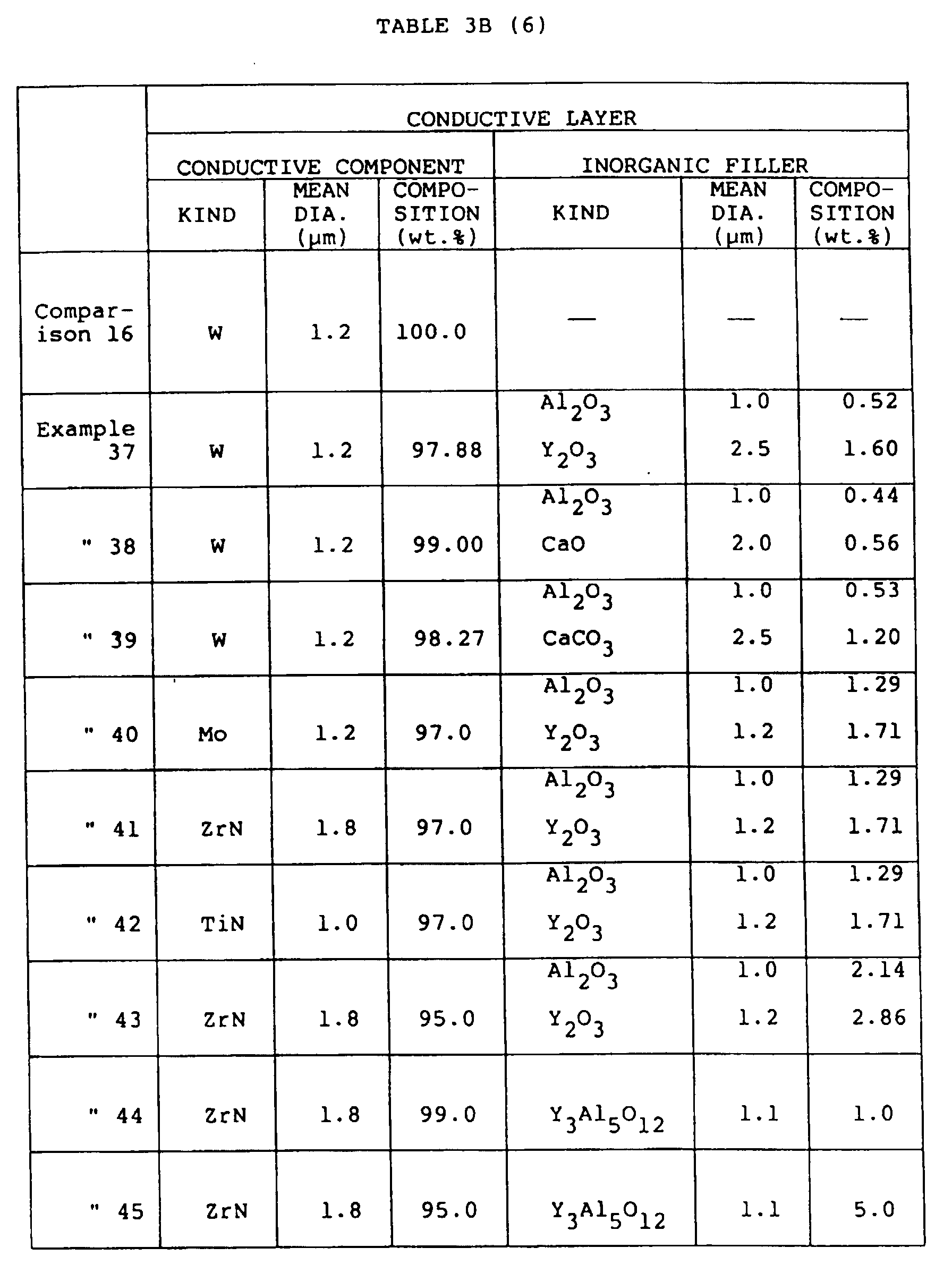

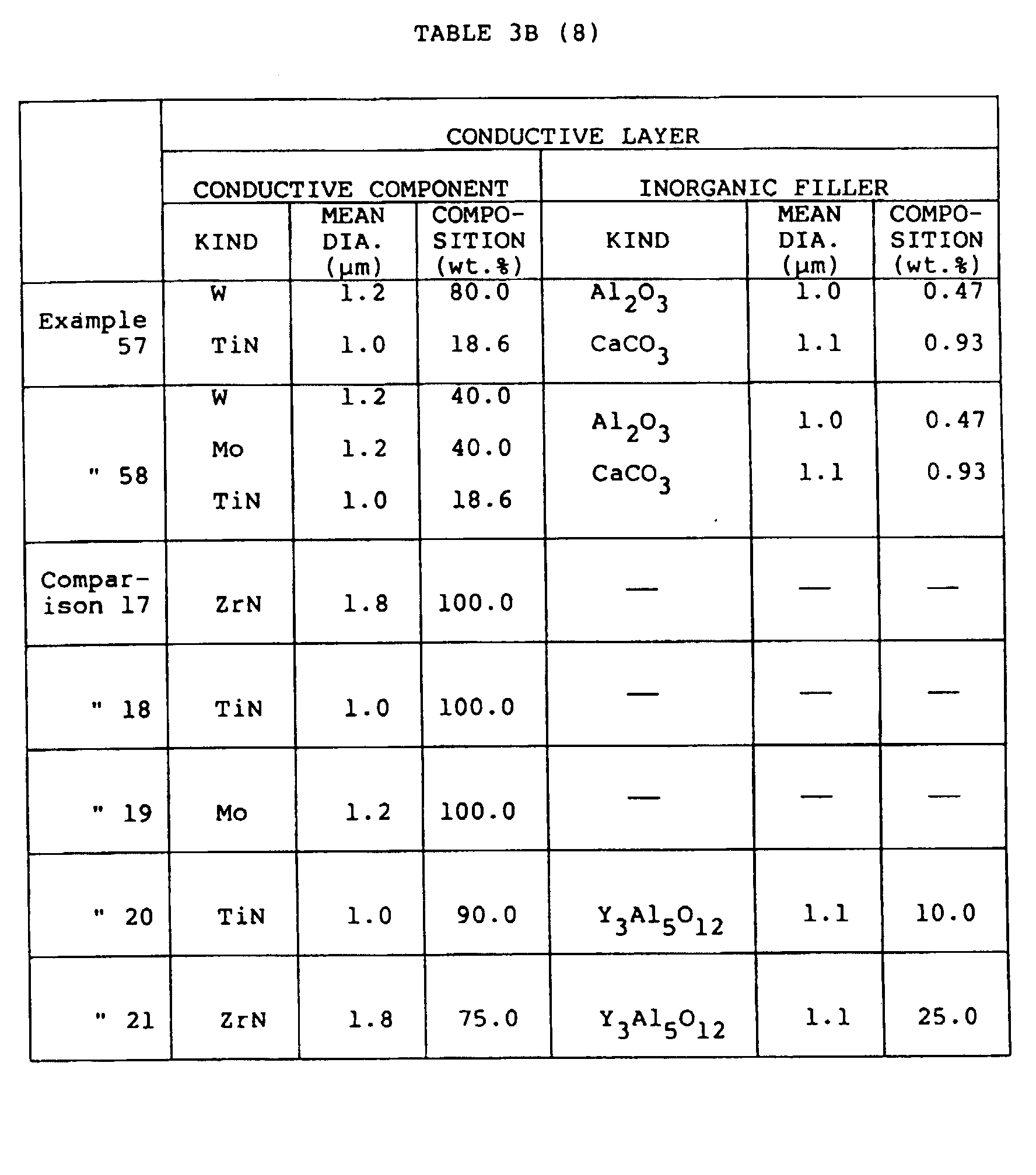

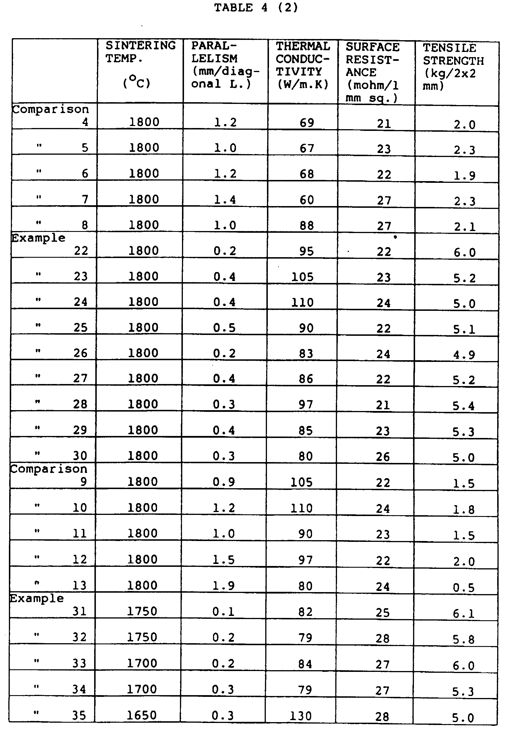


Claims (12)
- An aluminium nitride sintered body, comprising:(a) an insulating layer formed by sintering an aluminium nitride body; and(b) a metallized layer formed on said insulating layer, said metallized layer including a mixture of:(1) at least one conductive element and/or compound selected from W, Mo, Ta, TiN and ZrN; and(2) at least one inorganic filler including a compound containing a IIa, IIIa, IVa, IIIb, lanthanide or actinoide group element of the Periodic Table.
- The aluminium nitride sintered body as set forth in claim 1, wherein said insulating, layer includes at least one element selected from alkaline earth and rare earth group elements as a sintering aid.
- The aluminium nitride sintered body as set forth in claim 1, wherein said aluminium nitride sintered body is used as an electronic circuit substrate.
- The aluminium nitride sintered body as set forth in claim 3, wherein said at least one inorganic filler is any one or a mixture and a compound of alumina and at least one of rare-earth elements and alkaline-earth elements.
- The aluminium nitride sintered body as set forth in claim 1, wherein said conductive element is at least one element selected from Mo, W and Ta; and
said at least one inorganic filler is at least one element selected from IIIa, IIIb, IVa and actinoide group elements. - The aluminium nitride sintered body as set forth in claim 1, wherein said metallized layer is a multilayer.
- The aluminium nitride sintered body as set forth in claim 4, wherein the content of the mixture and/or the compound is 0.05 to 20 by weight percentage in terms of the corresponding oxide in said metallized layer.
- The aluminium nitride sintered body as set forth in claim 2, wherein the content of the rare-earth element and the alkaline-earth element is 0.01 to 15 by weight percentage in terms of the corresponding oxide in said metallized layer.
- The aluminium nitride sintered body as set forth in claim 1, wherein said insulating layer includes aluminium nitride and a sintering aid.
- The aluminium nitride sintered body as set forth in claim 9, wherein said sintering aid is at least one element selected from Y, La, Ce, Ca, Sr and Ba.
- The aluminium nitride sintered body as set forth in claim 9, wherein the rare-earth and,'or alkaline-earth elements included in said conductive layer are the same as the sintering aid elements included in said insulating layer.
- The aluminium nitride sintered body as set forth in claim 11, where in the rare-earth and/or alkaline-earth element included in said conductive layer is at least one of Y, La, Ce, Ca, Sr and Ba.
Applications Claiming Priority (6)
| Application Number | Priority Date | Filing Date | Title |
|---|---|---|---|
| JP3382686A JPS62197374A (en) | 1986-02-20 | 1986-02-20 | Aluminum nitride sintered body |
| JP33826/86 | 1986-02-20 | ||
| JP33824/86 | 1986-02-20 | ||
| JP3382486A JPS62197372A (en) | 1986-02-20 | 1986-02-20 | Manufacture of aluminum nitride sintered body with electroconductive metallized layer |
| JP61171914A JPH0738491B2 (en) | 1986-07-23 | 1986-07-23 | Method of manufacturing circuit board and circuit board |
| JP171914/86 | 1986-07-23 |
Publications (4)
| Publication Number | Publication Date |
|---|---|
| EP0235682A2 EP0235682A2 (en) | 1987-09-09 |
| EP0235682A3 EP0235682A3 (en) | 1988-08-17 |
| EP0235682B1 EP0235682B1 (en) | 1994-04-20 |
| EP0235682B2 true EP0235682B2 (en) | 1997-11-12 |
Family
ID=27288220
Family Applications (1)
| Application Number | Title | Priority Date | Filing Date |
|---|---|---|---|
| EP87102344A Expired - Lifetime EP0235682B2 (en) | 1986-02-20 | 1987-02-19 | Aluminium nitride sintered body having conductive metallized layer |
Country Status (4)
| Country | Link |
|---|---|
| US (1) | US4770953A (en) |
| EP (1) | EP0235682B2 (en) |
| KR (1) | KR900006122B1 (en) |
| DE (1) | DE3789628T3 (en) |
Families Citing this family (64)
| Publication number | Priority date | Publication date | Assignee | Title |
|---|---|---|---|---|
| JPS6265991A (en) * | 1985-09-13 | 1987-03-25 | 株式会社東芝 | High heat conductive ceramics substrate |
| JPS6318648A (en) * | 1986-07-11 | 1988-01-26 | Toshiba Corp | Circuit board using aluminum nitride |
| JPH0680873B2 (en) * | 1986-07-11 | 1994-10-12 | 株式会社東芝 | Circuit board |
| US5529852A (en) * | 1987-01-26 | 1996-06-25 | Sumitomo Electric Industries, Ltd. | Aluminum nitride sintered body having a metallized coating layer on its surface |
| CA1333241C (en) * | 1987-01-26 | 1994-11-29 | Akira Sasame | Aluminum nitride sintered body formed with metallized layer and method of manufacturing the same |
| US4906511A (en) * | 1987-02-12 | 1990-03-06 | Kabushiki Kaisha Toshiba | Aluminum nitride circuit board |
| US4883704A (en) * | 1987-03-30 | 1989-11-28 | Kabushiki Kaisha Toshiba | Circuit substrate comprising nitride type ceramics, method for preparing it, and metallizing composition for use in it |
| JPH0676790B2 (en) * | 1987-07-30 | 1994-09-28 | 株式会社東芝 | Igniter |
| JP2544398B2 (en) * | 1987-08-27 | 1996-10-16 | 富士通株式会社 | Method for metallizing A1N ceramics |
| US5017434A (en) * | 1988-01-27 | 1991-05-21 | Enloe Jack H | Electronic package comprising aluminum nitride and aluminum nitride-borosilicate glass composite |
| JPH01203270A (en) * | 1988-02-08 | 1989-08-16 | Sumitomo Electric Ind Ltd | Sintered aluminum nitride body having high thermal conductivity and its production |
| JP2949586B2 (en) * | 1988-03-07 | 1999-09-13 | 株式会社日立製作所 | Conductive material and manufacturing method thereof |
| US5264388A (en) * | 1988-05-16 | 1993-11-23 | Sumitomo Electric Industries, Inc. | Sintered body of aluminum nitride |
| US5272009A (en) * | 1988-10-21 | 1993-12-21 | Battelle Memorial Institute | Laminate material and its use as heat-sink |
| JP2765885B2 (en) * | 1988-11-14 | 1998-06-18 | 新光電気工業株式会社 | Aluminum nitride circuit board and method of manufacturing the same |
| JP2774560B2 (en) * | 1989-03-31 | 1998-07-09 | 株式会社東芝 | Aluminum nitride metallized substrate |
| US4908116A (en) * | 1989-06-01 | 1990-03-13 | The Board Of Trustees At The Leland Stanford Junior University | Capillary electrophoretic device employing structure permitting electrical contact through ionic movement |
| EP0421680B1 (en) * | 1989-09-27 | 1994-03-16 | Kabushiki Kaisha Toshiba | Aluminium nitride circuit board |
| US5830570A (en) * | 1989-12-19 | 1998-11-03 | Kyocera Corporation | Aluminum nitride substrate and process for preparation thereof |
| US5370907A (en) * | 1990-06-15 | 1994-12-06 | Sumitomo Electric Industries, Ltd. | Forming a metallized layer on an AlN substrate by applying and heating a paste of a metal composed of W and Mo |
| JPH0461293A (en) * | 1990-06-29 | 1992-02-27 | Toshiba Corp | Circuit board and manufacture thereof |
| US5200249A (en) * | 1990-08-15 | 1993-04-06 | W. R. Grace & Co.-Conn. | Via metallization for AlN ceramic electronic package |
| US5173354A (en) * | 1990-12-13 | 1992-12-22 | Cornell Research Foundation, Inc. | Non-beading, thin-film, metal-coated ceramic substrate |
| US5288769A (en) * | 1991-03-27 | 1994-02-22 | Motorola, Inc. | Thermally conducting adhesive containing aluminum nitride |
| US5616421A (en) * | 1991-04-08 | 1997-04-01 | Aluminum Company Of America | Metal matrix composites containing electrical insulators |
| US5775403A (en) * | 1991-04-08 | 1998-07-07 | Aluminum Company Of America | Incorporating partially sintered preforms in metal matrix composites |
| US5570502A (en) * | 1991-04-08 | 1996-11-05 | Aluminum Company Of America | Fabricating metal matrix composites containing electrical insulators |
| US5158912A (en) * | 1991-04-09 | 1992-10-27 | Digital Equipment Corporation | Integral heatsink semiconductor package |
| CA2113451A1 (en) * | 1991-09-12 | 1993-03-18 | Yi-Hung Chiao | Method of making co-fired, multilayer substrates |
| DE4138214A1 (en) * | 1991-11-21 | 1993-05-27 | Daimler Benz Ag | Metallisation of aluminium nitride ceramic - involves ceramic treatment to remove glass surface film |
| EP0640039A4 (en) * | 1992-05-12 | 1995-04-19 | Carborundum Co | Thin film metallization and brazing of aluminum nitride. |
| US5311399A (en) * | 1992-06-24 | 1994-05-10 | The Carborundum Company | High power ceramic microelectronic package |
| JPH06206772A (en) * | 1992-11-18 | 1994-07-26 | Toshiba Corp | Aluminum nitride sintered compact and ceramic circuit substrate |
| JPH0715101A (en) * | 1993-06-25 | 1995-01-17 | Shinko Electric Ind Co Ltd | Oxide ceramic circuit board and its manufacture |
| JP3724592B2 (en) * | 1993-07-26 | 2005-12-07 | ハイニックス セミコンダクター アメリカ インコーポレイテッド | Method for planarizing a semiconductor substrate |
| JP2634133B2 (en) * | 1993-08-03 | 1997-07-23 | 日本特殊陶業株式会社 | Aluminum nitride multilayer wiring board having high dielectric layer and method of manufacturing the same |
| JPH07142822A (en) * | 1993-09-20 | 1995-06-02 | Fujitsu Ltd | Circuit board and its manufacture |
| US5482903A (en) * | 1993-12-22 | 1996-01-09 | International Business Machines Corporation | Aluminum nitride body utilizing a vitreous sintering additive |
| JP3286651B2 (en) * | 1993-12-27 | 2002-05-27 | 株式会社住友金属エレクトロデバイス | Ceramic multilayer wiring board, method of manufacturing the same, and conductive material for ceramic multilayer wiring board |
| US5626943A (en) * | 1994-06-02 | 1997-05-06 | The Carborundum Company | Ultra-smooth ceramic substrates and magnetic data storage media prepared therefrom |
| EP0698590B1 (en) * | 1994-08-23 | 2003-10-22 | AT&T Corp. | Metallization of ceramics through application of an adherent reducible layer |
| US5552232A (en) * | 1994-12-21 | 1996-09-03 | International Business Machines Corporation | Aluminum nitride body having graded metallurgy |
| CN1139117C (en) * | 1995-03-20 | 2004-02-18 | 株式会社东芝 | Silicon nitride circuit substrate |
| KR100261793B1 (en) * | 1995-09-29 | 2000-07-15 | 니시무로 타이죠 | Circuit board with high strength and high reliability and process for preparing the same |
| JPH09260543A (en) * | 1996-03-22 | 1997-10-03 | Toshiba Corp | Aluminum nitride wiring board and its manufacture |
| US6033787A (en) * | 1996-08-22 | 2000-03-07 | Mitsubishi Materials Corporation | Ceramic circuit board with heat sink |
| JPH1067586A (en) * | 1996-08-27 | 1998-03-10 | Dowa Mining Co Ltd | Circuit base plate for power module and its production |
| US6323549B1 (en) * | 1996-08-29 | 2001-11-27 | L. Pierre deRochemont | Ceramic composite wiring structures for semiconductor devices and method of manufacture |
| US6143432A (en) * | 1998-01-09 | 2000-11-07 | L. Pierre deRochemont | Ceramic composites with improved interfacial properties and methods to make such composites |
| US5920037A (en) * | 1997-05-12 | 1999-07-06 | International Business Machines Corporation | Conductive bonding design for metal backed circuits |
| US6004624A (en) | 1997-07-02 | 1999-12-21 | International Business Machines Corporation | Method for the controlling of certain second phases in aluminum nitride |
| JP4812144B2 (en) * | 1998-07-22 | 2011-11-09 | 住友電気工業株式会社 | Aluminum nitride sintered body and manufacturing method thereof |
| US6506481B2 (en) | 2000-01-26 | 2003-01-14 | Ngk Spark Plug Co., Ltd. | Ceramic member for bonding, process for producing the same, vacuum switch, and vacuum vessel |
| US6485816B2 (en) * | 2000-01-31 | 2002-11-26 | Ngk Insulators, Ltd. | Laminated radiation member, power semiconductor apparatus, and method for producing the same |
| US6607836B2 (en) * | 2000-10-23 | 2003-08-19 | Ngk Insulators, Ltd. | Material of low volume resistivity, an aluminum nitride sintered body and a member used for the production of semiconductors |
| US20020185487A1 (en) * | 2001-05-02 | 2002-12-12 | Ramesh Divakar | Ceramic heater with heater element and method for use thereof |
| US6732914B2 (en) * | 2002-03-28 | 2004-05-11 | Sandia National Laboratories | Braze system and method for reducing strain in a braze joint |
| US6867978B2 (en) * | 2002-10-08 | 2005-03-15 | Intel Corporation | Integrated heat spreader package for heat transfer and for bond line thickness control and process of making |
| US7532481B2 (en) * | 2004-04-05 | 2009-05-12 | Mitsubishi Materials Corporation | Al/AlN joint material, base plate for power module, power module, and manufacturing method of Al/AlN joint material |
| US20070251938A1 (en) * | 2006-04-26 | 2007-11-01 | Watlow Electric Manufacturing Company | Ceramic heater and method of securing a thermocouple thereto |
| US10037928B2 (en) * | 2015-01-29 | 2018-07-31 | Kyocera Corporation | Circuit board and electronic device |
| CN109487198B (en) * | 2018-12-20 | 2024-01-30 | 西安赛尔电子材料科技有限公司 | Preparation method of rare earth metal-molybdenum binary infiltration layer for kovar alloy surface |
| CN114538933B (en) * | 2020-11-24 | 2022-11-22 | 娄底市安地亚斯电子陶瓷有限公司 | Method for manufacturing travelling wave tube clamping rod |
| CN116410003A (en) * | 2021-12-31 | 2023-07-11 | 江苏博睿光电股份有限公司 | Substrate, preparation method and application |
Family Cites Families (6)
| Publication number | Priority date | Publication date | Assignee | Title |
|---|---|---|---|---|
| US3927815A (en) * | 1971-11-22 | 1975-12-23 | Ngk Insulators Ltd | Method for producing multilayer metallized beryllia ceramics |
| JPS5811390B2 (en) * | 1977-02-18 | 1983-03-02 | 株式会社東芝 | Method of manufacturing thermally conductive substrate |
| JPS5848926A (en) * | 1981-09-18 | 1983-03-23 | Hitachi Ltd | Insulated type semiconductor device |
| DE3247985C2 (en) * | 1982-12-24 | 1992-04-16 | W.C. Heraeus Gmbh, 6450 Hanau | Ceramic carrier |
| US4659611A (en) * | 1984-02-27 | 1987-04-21 | Kabushiki Kaisha Toshiba | Circuit substrate having high thermal conductivity |
| JPS61142759A (en) * | 1984-12-14 | 1986-06-30 | Ngk Spark Plug Co Ltd | Substrate for ic package |
-
1987
- 1987-02-19 US US07/016,557 patent/US4770953A/en not_active Expired - Lifetime
- 1987-02-19 EP EP87102344A patent/EP0235682B2/en not_active Expired - Lifetime
- 1987-02-19 DE DE3789628T patent/DE3789628T3/en not_active Expired - Fee Related
- 1987-02-20 KR KR1019870001437A patent/KR900006122B1/en not_active IP Right Cessation
Also Published As
| Publication number | Publication date |
|---|---|
| KR900006122B1 (en) | 1990-08-24 |
| US4770953A (en) | 1988-09-13 |
| EP0235682A2 (en) | 1987-09-09 |
| DE3789628T2 (en) | 1994-09-01 |
| EP0235682A3 (en) | 1988-08-17 |
| EP0235682B1 (en) | 1994-04-20 |
| KR870008055A (en) | 1987-09-24 |
| DE3789628D1 (en) | 1994-05-26 |
| DE3789628T3 (en) | 1998-04-02 |
Similar Documents
| Publication | Publication Date | Title |
|---|---|---|
| EP0235682B2 (en) | Aluminium nitride sintered body having conductive metallized layer | |
| KR900005842B1 (en) | Aluminium nitride substrade | |
| JPWO2002045470A1 (en) | Substrate and method of manufacturing the same | |
| JPH04212441A (en) | Ceramic wiring board | |
| JPH0823145A (en) | Substrate for hybrid ic | |
| JP3618422B2 (en) | High strength circuit board and manufacturing method thereof | |
| JPH0369873B2 (en) | ||
| JP4950379B2 (en) | AlN metallized substrate and manufacturing method thereof | |
| JP2704159B2 (en) | Aluminum nitride sintered body having conductive metallized layer and method of manufacturing the same | |
| JPH1153940A (en) | Copper metalized composition and glass ceramic wiring board using it | |
| JPH0738491B2 (en) | Method of manufacturing circuit board and circuit board | |
| JPH08109084A (en) | Aluminum nitride sintered material having electrically conductive metallized layer and its manufacture | |
| JPH05221759A (en) | Aluminum nitride substrate with metallizing layer and metallizing method | |
| JP3709062B2 (en) | Aluminum nitride wiring board and manufacturing method thereof | |
| JPH03116608A (en) | Conductor paste and conductor | |
| JP3908755B2 (en) | High strength circuit board | |
| JPH0723273B2 (en) | Method for metallizing aluminum nitride substrate | |
| JP3678485B2 (en) | High strength and high reliability circuit board and manufacturing method thereof | |
| JP4116656B2 (en) | High-strength circuit board and manufacturing method thereof | |
| JP2892220B2 (en) | Manufacturing method of ceramic wiring board | |
| JP2004175599A (en) | Process for manufacturing ceramic sintered compact having metallized layer | |
| JP4126588B2 (en) | Aluminum nitride sintered body having metallized layer and method for producing the same | |
| JP2002179467A (en) | METALLIZED AlN SUBSTRATE AND ITS PRODUCTION PROCESS | |
| JP2003342088A (en) | Aluminum nitride sintered compact having metallized layer and method for producing the same | |
| JP2003342073A (en) | Aluminum nitride sintered compact having metallized layer and its manufacturing process |
Legal Events
| Date | Code | Title | Description |
|---|---|---|---|
| PUAI | Public reference made under article 153(3) epc to a published international application that has entered the european phase |
Free format text: ORIGINAL CODE: 0009012 |
|
| AK | Designated contracting states |
Kind code of ref document: A2 Designated state(s): DE GB |
|
| PUAL | Search report despatched |
Free format text: ORIGINAL CODE: 0009013 |
|
| AK | Designated contracting states |
Kind code of ref document: A3 Designated state(s): DE GB |
|
| 17P | Request for examination filed |
Effective date: 19881201 |
|
| 17Q | First examination report despatched |
Effective date: 19900927 |
|
| GRAA | (expected) grant |
Free format text: ORIGINAL CODE: 0009210 |
|
| AK | Designated contracting states |
Kind code of ref document: B1 Designated state(s): DE GB |
|
| REF | Corresponds to: |
Ref document number: 3789628 Country of ref document: DE Date of ref document: 19940526 |
|
| PLBI | Opposition filed |
Free format text: ORIGINAL CODE: 0009260 |
|
| 26 | Opposition filed |
Opponent name: HOECHST AG Effective date: 19950120 |
|
| PLAW | Interlocutory decision in opposition |
Free format text: ORIGINAL CODE: EPIDOS IDOP |
|
| PLAW | Interlocutory decision in opposition |
Free format text: ORIGINAL CODE: EPIDOS IDOP |
|
| PUAH | Patent maintained in amended form |
Free format text: ORIGINAL CODE: 0009272 |
|
| STAA | Information on the status of an ep patent application or granted ep patent |
Free format text: STATUS: PATENT MAINTAINED AS AMENDED |
|
| 27A | Patent maintained in amended form |
Effective date: 19971112 |
|
| AK | Designated contracting states |
Kind code of ref document: B2 Designated state(s): DE GB |
|
| REG | Reference to a national code |
Ref country code: GB Ref legal event code: 746 Effective date: 19981007 |
|
| REG | Reference to a national code |
Ref country code: GB Ref legal event code: IF02 |
|
| PGFP | Annual fee paid to national office [announced via postgrant information from national office to epo] |
Ref country code: GB Payment date: 20030219 Year of fee payment: 17 |
|
| PGFP | Annual fee paid to national office [announced via postgrant information from national office to epo] |
Ref country code: DE Payment date: 20030227 Year of fee payment: 17 |
|
| PG25 | Lapsed in a contracting state [announced via postgrant information from national office to epo] |
Ref country code: GB Free format text: LAPSE BECAUSE OF NON-PAYMENT OF DUE FEES Effective date: 20040219 |
|
| PG25 | Lapsed in a contracting state [announced via postgrant information from national office to epo] |
Ref country code: DE Free format text: LAPSE BECAUSE OF NON-PAYMENT OF DUE FEES Effective date: 20040901 |
|
| GBPC | Gb: european patent ceased through non-payment of renewal fee |
Effective date: 20040219 |