EP0233649A2 - IC-Incorporated memory card - Google Patents
IC-Incorporated memory card Download PDFInfo
- Publication number
- EP0233649A2 EP0233649A2 EP87102400A EP87102400A EP0233649A2 EP 0233649 A2 EP0233649 A2 EP 0233649A2 EP 87102400 A EP87102400 A EP 87102400A EP 87102400 A EP87102400 A EP 87102400A EP 0233649 A2 EP0233649 A2 EP 0233649A2
- Authority
- EP
- European Patent Office
- Prior art keywords
- protective cover
- contact terminals
- electroconductive
- short
- memory card
- Prior art date
- Legal status (The legal status is an assumption and is not a legal conclusion. Google has not performed a legal analysis and makes no representation as to the accuracy of the status listed.)
- Granted
Links
Images


Classifications
-
- G—PHYSICS
- G06—COMPUTING; CALCULATING OR COUNTING
- G06K—GRAPHICAL DATA READING; PRESENTATION OF DATA; RECORD CARRIERS; HANDLING RECORD CARRIERS
- G06K19/00—Record carriers for use with machines and with at least a part designed to carry digital markings
- G06K19/06—Record carriers for use with machines and with at least a part designed to carry digital markings characterised by the kind of the digital marking, e.g. shape, nature, code
- G06K19/067—Record carriers with conductive marks, printed circuits or semiconductor circuit elements, e.g. credit or identity cards also with resonating or responding marks without active components
- G06K19/07—Record carriers with conductive marks, printed circuits or semiconductor circuit elements, e.g. credit or identity cards also with resonating or responding marks without active components with integrated circuit chips
- G06K19/077—Constructional details, e.g. mounting of circuits in the carrier
- G06K19/07743—External electrical contacts
-
- Y—GENERAL TAGGING OF NEW TECHNOLOGICAL DEVELOPMENTS; GENERAL TAGGING OF CROSS-SECTIONAL TECHNOLOGIES SPANNING OVER SEVERAL SECTIONS OF THE IPC; TECHNICAL SUBJECTS COVERED BY FORMER USPC CROSS-REFERENCE ART COLLECTIONS [XRACs] AND DIGESTS
- Y10—TECHNICAL SUBJECTS COVERED BY FORMER USPC
- Y10S—TECHNICAL SUBJECTS COVERED BY FORMER USPC CROSS-REFERENCE ART COLLECTIONS [XRACs] AND DIGESTS
- Y10S439/00—Electrical connectors
- Y10S439/93—Coupling part wherein contact is comprised of a wire or brush
Definitions
- Steps 20 are formed at the respective forward side portions of protective cover l2, so that they can be brought into abutting engagement with associated projections (not shown) of a card-insertion slit of an external device (not shown) when the IC card is inserted thereinto.
- steps 20 of protective cover l2 are in abutment with the corresponding associate projections provided within the card insertion slit.
- Figs. 7 and 8 show a second modified form of the short-circuiting member.
- Short-circuiting member 38 has leaf spring-like member 40 which is formed of electroconductive material.
- Member 40 is comprised of attachment end edge section 40a and contact end edge section 40b. Attachment end edge section 40a is attached to bottom surface l2a of protective cover l2 and, when protective cover l2 covers contact terminal 8a, are placed in contact with contact terminal 8a, whereby contact terminals 8a are short-circuited.
Abstract
Description
- This invention relates to an IC (integrated circuit)-incorporated memory card known as an IC card and, in particular, to a memory card equipped with an IC including a memory element, such as a ROM (read-only memory) or RAM (random-access memory), and a control element, such as a CPU (central processing unit).
- An IC card has been recently developed which comprises a card body having an IC incorporated therein. This IC includes a memory element, such as a ROM or RAM, and a control element, such as a CPU. This type of IC includes a plurality of terminals for permitting the internal and external transfer of electric signals. The respective IC terminals are electrically connected to a plurality of electric signal-carrying members which possess contact terminals for electrical connection to a card information processing unit.
- Since the contact terminals of this type of IC card are exposed on the surface of the card body, it is necessary to protect them from adverse enviromental factors, such as contamination, dirt, static electricity, etc. Japanese Utility Model Disclosure (Kokai) No. 59-70262, for example discloses this type of an IC card having a protective cover which allows the respective contact terminals to be exposed when the IC card is in use and covers them when the card is not being used.
- The aforementioned protective cover is sufficient to protect the contract terminals from contamination, dirt, and dust, but cannot protect them from static electricity. That is, this protective cover is usually of such a type that the insulation distance between the end of the cover and the respective contact terminals is insufficient. Therefore, even if the contact terminals are covered by the protective cover, there is a risk that when the user's hand touches that portion of the card body, for example, in the neighborhood of the protective cover, a discharge will occur at the contact terminal, through a clearance between the cover end and the card body, due to the static electricity on the user's body. This may cause breakdown of the IC within the IC card.
- It is accordingly the object of the present invention to provide a memory card which can be made substantially free from the effects of external static electricity.
- According to an aspect of the present invention, there is provided a memory card for use in a card information-processing unit to allow the information contained in the card to be processed, comprising a card body, at least one integrated circuit incorporated in the card body and having a plurality of internal and external signal-connection terminals, a plurality of electric signal-carrying members electrically connected to respective terminals of the integrated circuit, and having contact terminals for electrical connection to the card information-processing unit, the contact terminals being exposed in a predetermined pattern on a portion of the main surface of the card body, a protective cover having a surface facing the main surface of the card body, and being slidably movable in two predetermined directions thereon, so that, by being movable in one direction, the respective contact terminals may be exposed when the memory card is in use, and being movable in the other direction, the respective contact terminals may be covered when the memory card is not being used, and short-circuiting means provided on the surface of the protective cover, for electrically short-circuiting the respective contact terminals with respect to each other when the protective cover covers the respective contact terminals.
- In the memory card of the present invention, the short-circuiting member is slidably movable on the main surface of the card body, with the result that the contact terminals may be electrically short-circuited when the memory card is not in use, and may be open-circuited only when the memory card is being used.
- For this reason, when the memory card is not being used, the contact terminals are electrically short-circuited, and thus are all at the same potential level. This specific arrangement is less liable to be affected by external static electricity than in the case where the contact terminals are not short-circuited. As a result, the internal integrated circuit can be protected from damage caused by external static electricity.
- This invention can be more fully understood from the following detailed description when taken in conjunction with the accompanying drawings, in which:
- Fig. l is a perspective view of a memory card according to one embodiment of the present invention;
- Fig. 2 is a perspective view showing the memory card with a protective cover displaced;
- Fig. 3 is a perspective view, partly cutaway and partly in section, showing the memory card of Fig. l;
- Fig. 4 is a cross-sectional view, partly cutaway, showing the memory card of Fig. l;
- Fig. 5 is a perspective view showing a first modified form of a short-circuiting member of the memory card;
- Fig. 6 is a cross-sectional view of the first modified form of the short-circuiting member Fig. 5;
- Fig. 7 is a perspective view showing a second modified form of the short-circuiting member of the memory card;
- Fig. 8 is a cross-sectional view of the second modified form of the short-circuiting member shown in Fig. 7;
- Fig. 9 is a perspective view showing a third modified form of the short-circuiting member of the memory card;
- Fig. l0 is a cross-sectional view of the third modified form of the short-circuiting member shown in Fig. 9;
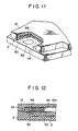
- Fig. ll is a perspective view showing a fourth modified form of the short-circuiting member;
- Fig. l2 is a cross-sectional view of the fourth modified form of the short-circuiting member shown in Fig. ll;
- Fig. l3 is a perspective view showing a fifth modified form of the short-circuiting member of the memory card;
- Fig. l4 is a cross-sectional view of the fifth modified form of the short-circuiting member shown in Fig. l3;
- Figs. l5 and l6 respectively show a view of a pattern corresponding to a rectangular pile array on the third to fifth modifications of the short-circuiting member of the memory card; and
- Figs. l7 and l8 respectively show a view of a pattern corresponding to an alternately staggered or offset pile array on the third to fifth modifications of the short-circuiting member of the memory card.
- The memory card according to the embodiment of the present invention will be explained below, with reference to the accompanying drawing sheets.
- Figs. l and 2 show an example of the IC-incorporated memory card according to the embodiment of the present invention. IC 4 having a memory element, such as a ROM or RAM, and
IC 6 having a control element, such as a CPU, are incorporated incard body 2.ICs contact terminals 4a and 6a, respectively, for allowing the internal and external transmission of external signals.Respective terminals 4a and 6a are electrically connected to a plurality of electric signal-carrying members 8 (see Fig. 4) which havecontact terminals 8a for electric connection to a card information-processing unit (not shown).Contact terminals 8a are exposed on upper surface 2a ofcard body 2. Cover l0 is mounted relative to upper surface 2a ofcard body 2, with a predetermined spacing left therebetween, noting that the aforementioned spacing corresponds to the thickness of protective cover l2, as will be set out below. Cover l0 is mounted such that it wholly covers upper surface 2a ofcard body 2, except for an area ofcontact terminals 8a. Cover l0 may be formed either integral with, or separately from,card body 2. - Provided between
card body 2 and cover l0 is protective cover l2, for example, a nonconductive sheet-like member, which slides in the direction indicated by the arrow shown in Fig. l. Protective cover l2 is normally located so that is coverscontact terminals 8a, as shown in Fig. l, when the IC card is not being used, in order to protect them from the external environment. When the IC card is to be used, however, protective cover l2 is shifted to a position wherebycontact terminals 8a are exposed, as is shown in Fig. 2. Spring l4 is positioned on cover l0 such that it is fixed at one end tocard body 2 and at the other end to protective cover l2. Protective cover l2 is held, under the action of spring l4, in the state shown in Fig. l. If, when in this state, protective cover l2 is slidably displaced, under the action of spring l4, in the direction indicated by the arrow in Fig. l, then protective cover l2 is moved to exposecontact terminals 8a, as is shown in Fig. l2. - Projections l6 are provided one pair at each side edge of the upper surface of the forward end portion of
card body 2, and recesses l8 are formed one at each forward side edge portion of the bottom surface of protective cover l2, to allow projections l6 to be snap-fitted into associated recesses l8 when protective cover l2 is located in the position shown in Fig. l. Thus, when the IC card is not being used, protective cover l2 is held in the position shown in Fig. l, so as to prevent it from being displaced inadvertently. -
Steps 20 are formed at the respective forward side portions of protective cover l2, so that they can be brought into abutting engagement with associated projections (not shown) of a card-insertion slit of an external device (not shown) when the IC card is inserted thereinto. Stated in more detail, in the state as shown in Fig. l, the IC card is inserted into the card-insertion slit, and when it reaches the predetermined position where the aforementioned associated projections are located,steps 20 of protective cover l2 are in abutment with the corresponding associate projections provided within the card insertion slit. When the IC card is pushed further forward, projections l6 ofcard body 2 are moved ahead, beyond recesses l8 of protective cover l2, causing the protective cover to be displaced in the direction of the arrow shown in Fig. l, to thereby permitcontact terminals 8a oncard body 2 to be exposed. With the IC card thus having been moved to its prescribed position, spring terminals (not shown) provided within the card-insertion slit are brought into contact withcontact terminals 8a oncard body 2. When the IC card is to be withdrawn from the card-insertion slit, after usage, it is drawn back to a position where steps 20 of protective cover l2 are brought out of abutment with the projections provided within the card-insertion slit. Upon further withdrawal of the IC card from the card-insertion slit, protective cover l2 automatically regains its original position, due to the action of spring l4, at which time projections l6 ofcard body 2 snap-fit into recesses l8 of protective cover l8. As a result, when the IC card is completely withdrawn from the card-insertion slit,contact terminals 8a are again covered by protective cover l2, as shown in Fig. l. - Figs. 3 and 4 show in detail an internal arrangement of protective cover l2.
Recess 22 is formed at buttom surface l2a of protective cover l2, and, at the very least, corresponds to contactterminals 8a, as can be appreciated from Fig. l. Short-circuitingmember 24 is provided withinrecess 22, and is adapted to electrically short-circuitrespective contact terminals 8a when protective cover l2 is in the state shown in Fig. l. Short-circuitingmember 24 includes a plurality of leaf spring-like,electroconductive contact terminals 26 and anelectroconductive member 28. Therespective contact terminals 26, when being located opposite tocorresponding contact terminals 8a, are in independent electrical contact with theircorresponding contact terminals 8a.Contact terminals 26 are welded at their rear ends to electroconductivemember 28 which electrically short-circuits members 26. Short-circuitingmember 24 is fixed byelectroconductive member 28 to protective cover l2, so thatmember 24 may be moved together with cover l2. Short-circuitingmember 24 short-circuits contact terminals 8a, as shown in Fig. 3, when protective cover l2 is in the state shown in Fig. l, and open-circuits contact terminals 8a when short-circuitingmember 24 is moved to the position shown in Fig. 2. - In the aforementioned memory card thus arranged,
contact terminals 8a are short-circuited when the IC card is not being used, so that they are all placed at the same potential level. This particular arrangement is less liable to be influenced by the effects of external static electricity than whencontact terminals 8a are not short-circuited. As a result,internal ICs - Figs. 5 and 6 show a first modified form of the short-circuiting member. Short-circuiting
member 32 includesspring member 34 which is formed of electroconductive material and is comprised ofelectroconductive section 34a and a plurality ofcontact terminals 34b.Electroconductive section 34a of short-circuitingmember 32 is attached to bottom surface l2a of protective cover l2, and the plurality ofcontact terminals 34b extend fromelectroconductive section 34a and, when protective cover l2 coverscontact terminals 8a, are in contact withcontact terminals 8, wherebycontact terminals 8a are short-circuited. - Figs. 7 and 8 show a second modified form of the short-circuiting member. Short-circuiting
member 38 has leaf spring-like member 40 which is formed of electroconductive material.Member 40 is comprised of attachment end edge section 40a and contactend edge section 40b. Attachment end edge section 40a is attached to bottom surface l2a of protective cover l2 and, when protective cover l2 coverscontact terminal 8a, are placed in contact withcontact terminal 8a, wherebycontact terminals 8a are short-circuited. - Figs. 9 and l0 show a third modified form of the short-circuiting member. In short-circuiting
member 42, protective cover l2 is formed of electroconductive member, such as a metal, and a greater number ofelectroconductive piles 44 are attached to bottom surface l2a ofrecess 22 of protective cover l2. When protective cover l2 coverscontact terminals 8a, piles 44 are in contact withcontact terminals 8a, wherebycontact terminals 8a are short-circuited. - Figs. ll and l2 show a fourth modified form of the short-circuiting member. In short-
circuiting circuit 46, protective cover l2 is formed of a nonconductive member and, on bottom surface l2a ofrecess 22 of cover l2, electroconductive material is coated, painted, or plated, to thereby formelectroconductive layer 48 withelectroconductive piles 50 attached thereto. Whencontact terminals 8a are covered by protective cover l2, piles 50 are in contact withcontact terminals 8a, wherebycontact terminals 8a are short-circuited. - Figs. l3 and 14 show a fifth modified form of the short-circuiting member. In short-circuiting
member 52, electroconductive piles 56 are attached by electroconductive adhesive 54 to bottom surface l2a ofrecess 22 of protective cover l2.Piles 56 are placed in contact withcontact terminals 8a when protective cover l2 coverscontact terminals 8a, wherebycontact terminals 8a are short-circuited. - In the modifications of Figs. 3 to 5,
respective piles rectangular pattern 58 covering a complete array ofrespective contact terminals 8a, as shown in Figs. l5 and l6, or to provide alternately staggered or offsetpattern 58 covering a complete array ofrespective contact patterns 8a, as shown in Figs. l7 and l8. In the alternately staggered or offsetpattern 58, as shown in Figs. l7 and l8, for example, it is necessary only to move protective cover l2 over a shorter distance than in the case of the array shown in Figs. l5 and l6. That is, ℓl > ℓ2
where
ℓl signifies the moving distance for the array of Figs. l5 and l6; and
ℓ2 signifies the moving distance for the array of Figs. l7 and l8.
Claims (10)
a card body (2) having a main surface (2a);
at least one integrated circuit (4, 6) incorporated in the card body (2), and having a plurality of internal and external signal-connection terminals (4a, 6a);
a plurality of electric signal-carrying members (8) electrically connected to respective terminals (4a, 6a) of the integrated circuit (4, 6), and having contact terminals (8a) for electrical connection to the card information-processing unit, the contact terminals (8a) being exposed in a predetermined pattern on the main surface (2a) of the card body (2); and
a protective cover (l2) having a surface (l2a) facing the main surface (2a) of the card body (2), and being slidably movable in two predetermined directions on the main surface (2a) of the card body (2), the protective cover (l2) being movable in one of the two directions, so that when the memory card is being used, the respective contact terminals (8a) may be exposed, and being movable in the other direction, so that when the memory card is not being used, the respective contact terminals (8a) may be covered;
characterized by further comprising
short-circuiting means (24, 32, 38, 42, 46, 52) provided on the surface (l2a) of the protective cover (l2), for electrically short-circuiting the respective contact terminals (8a) when the protective cover (l2) covers the respective contact terminals (8a).
characterized in that said short-circuiting means (24) is comprised of an electroconductive member (28) attached to that surface (l2a) of said protective cover (l2) which faces the contact terminals (8a), and a plurality of leaf spring-like contact terminals (26) of electroconductive material which are brought into contact with the contact terminals (8a) when said protective cover (l2) covers said contact terminals (8a).
characterized in that said respective leaf spring-like contact terminals (26) are welded to said electroconductive member (28).
characterized in that said short-circuiting means (34) has an electroconductive spring member (34) comprised of an electroconductive portion 34a attached to the facing surface (l2a) of the protective cover (l2), and a plurality of contact terminal portions (34b) extending from the electroconductive portion 34a, and adapted to be brought into contact with said contact terminals (8a) when said protective cover (l2) covers said contact terminals (8a).
characterized in that said short-circuiting means (38) has a leaf spring-like member (40) of electroconductive material, which is comprised of an attachment end edge portion 40a attached to the facing surface (l2a) of said protective cover (l2), and a contact end edge portion 40b adapted to be brought into contact with said respective contact terminals (8a) when said protective cover (l2) covers said contact terminals (8a).
characterized in that said protective cover (l2) is made of electroconductive material, and said short-circuiting member (42) includes electroconductive piles (44) attached to said protective cover (l2), and adapted to be brought into contact with said contact terminals (8a) when said protective cover (l2) covers said contact terminals (8a).
characterized in that said electroconductive piles (44) are attached to said protective cover (l2), in a pattern corresponding to a particular array of said contact terminals (8a).
characterized in that said protective cover (l2) is made of nonconductive material, and said short-circuiting means (46) is comprised of an electroconductive portion (48) coated as an electroconductive layer (48) on said facing surface (l2a) of said protective cover (l2), and electroconductive piles (50) attached to said electroconductive layer (48), and adapted to be brought into contact with said contact terminals (8a) when said protective cover (l2) covers said contact terminals (8a).
characterized in that said short-circuiting means (52) is comprised of a number of electroconductive piles (56) adapted to be brought into contact with said contact terminals (8a) when said protective cover (l2) covers said contact terminals (8a), and an electroconductive adhesive (54) for bonding the electroconductive piles (56) to the facing surface (l2a) of said protective cover (l2), so that the electroconductive piles (56) may be short-circuited.
characterized in that said at least one integrated circuit (4, 6) includes at least one of a memory element, such as a read-only memory or a random-access memory, and a control element, such as a central processing unit.
Applications Claiming Priority (2)
| Application Number | Priority Date | Filing Date | Title |
|---|---|---|---|
| JP36665/86 | 1986-02-21 | ||
| JP61036665A JPH0698865B2 (en) | 1986-02-21 | 1986-02-21 | Memory card |
Publications (3)
| Publication Number | Publication Date |
|---|---|
| EP0233649A2 true EP0233649A2 (en) | 1987-08-26 |
| EP0233649A3 EP0233649A3 (en) | 1989-06-14 |
| EP0233649B1 EP0233649B1 (en) | 1991-12-04 |
Family
ID=12476153
Family Applications (1)
| Application Number | Title | Priority Date | Filing Date |
|---|---|---|---|
| EP87102400A Expired - Lifetime EP0233649B1 (en) | 1986-02-21 | 1987-02-20 | Ic-incorporated memory card |
Country Status (4)
| Country | Link |
|---|---|
| US (1) | US4780604A (en) |
| EP (1) | EP0233649B1 (en) |
| JP (1) | JPH0698865B2 (en) |
| DE (1) | DE3774893D1 (en) |
Cited By (8)
| Publication number | Priority date | Publication date | Assignee | Title |
|---|---|---|---|---|
| EP0312067A2 (en) * | 1987-10-16 | 1989-04-19 | Sumitomo Metal Industries, Ltd. | Metal case for housing an IC and a manufacturing method therefor |
| FR2625840A1 (en) * | 1988-01-13 | 1989-07-13 | Sgs Thomson Microelectronics | HOUSING FOR CONTAINING A FRAGILE ELEMENT SUCH AS A LOGIC CIRCUIT AND METHOD FOR ASSEMBLING SUCH A HOUSING |
| EP0338080A1 (en) * | 1987-08-31 | 1989-10-25 | Fanuc Ltd. | Ic card |
| EP0384894A1 (en) * | 1989-02-24 | 1990-08-29 | Ascom Autophon Ag | Subscriber telephone arrangement |
| EP0409241A1 (en) * | 1989-07-19 | 1991-01-23 | Kabushiki Kaisha Toshiba | IC card with additional terminals and method of controlling the IC card |
| US5920460A (en) * | 1997-01-11 | 1999-07-06 | Methode Electronics, Inc. | PC card receptacle with integral ground clips |
| USRE36540E (en) * | 1993-07-15 | 2000-02-01 | Methode Electronics, Inc. | Method of manufacturing a memory card package |
| WO2007065763A1 (en) * | 2005-12-06 | 2007-06-14 | International Business Machines Corporation | An adapter to improve electrostatic discharge protection |
Families Citing this family (35)
| Publication number | Priority date | Publication date | Assignee | Title |
|---|---|---|---|---|
| JPH0657476B2 (en) * | 1987-03-27 | 1994-08-03 | 三菱電機株式会社 | IC card external device connector |
| JPS63242692A (en) * | 1987-03-31 | 1988-10-07 | 三菱電機株式会社 | Semiconductor-device card |
| JPH0418235Y2 (en) * | 1988-04-08 | 1992-04-23 | ||
| US4931991A (en) * | 1988-12-22 | 1990-06-05 | Amp Incorporated | Machine readable memory card with capacitive interconnect |
| US6938825B1 (en) | 1989-04-24 | 2005-09-06 | Ultracard, Inc. | Data system |
| US5157244A (en) * | 1989-12-19 | 1992-10-20 | Amp Incorporated | Smart key system |
| US5257414A (en) * | 1990-11-26 | 1993-10-26 | Motorola, Inc. | Apparatus for accepting and retaining a memory card |
| JPH04263998A (en) * | 1991-02-19 | 1992-09-18 | Mitsubishi Electric Corp | Memory card |
| US5163850A (en) * | 1991-04-18 | 1992-11-17 | Polaroid Corporation | Electrostatic discharge protection devices for semiconductor chip packages |
| US5414253A (en) * | 1991-12-03 | 1995-05-09 | Texas Instruments Incorporated | Integrated circuit card |
| US5289336A (en) * | 1992-01-14 | 1994-02-22 | Harris Corporation | Static electricity dispersant |
| US5526235A (en) * | 1994-06-23 | 1996-06-11 | Garmin Communication And Navigation | Electronic storage device and receptacle |
| FR2721731B1 (en) * | 1994-06-24 | 1996-08-09 | Schlumberger Ind Sa | Memory card. |
| WO1997040466A1 (en) * | 1996-04-19 | 1997-10-30 | Siemens Aktiengesellschaft | Card reading device |
| EP0803834A3 (en) * | 1996-04-25 | 2000-06-28 | Olympus Optical Co., Ltd. | Memory card installing device |
| US5894597A (en) * | 1996-09-24 | 1999-04-13 | Motorola, Inc. | Communication device for different sized cards |
| US5812357A (en) * | 1996-10-11 | 1998-09-22 | Polaroid Corporation | Electrostatic discharge protection device |
| JP3173438B2 (en) * | 1997-06-04 | 2001-06-04 | ソニー株式会社 | Memory card and mounting device |
| US6786417B1 (en) * | 1997-06-04 | 2004-09-07 | Sony Corporation | Memory card with write protection switch |
| US5963415A (en) * | 1997-07-05 | 1999-10-05 | Polaroid Corporation | Electrostatic discharge protection device |
| US6871787B1 (en) | 1998-07-10 | 2005-03-29 | Ultracard, Inc. | Data storage card having a glass substrate and data surface region and method for using same |
| US6282097B1 (en) | 1998-10-28 | 2001-08-28 | Garmin Corporation | Data card having a retractable handle |
| US6215671B1 (en) | 1998-12-10 | 2001-04-10 | Garmin Corporation | Method and apparatus for connecting circuit boards |
| US6250553B1 (en) | 1998-12-30 | 2001-06-26 | Garmin Corporation | Data card having a retractable handle |
| DE60042139D1 (en) * | 1999-02-19 | 2009-06-18 | Nippon Telegraph & Telephone | Contactless chip card and system for this |
| US7036739B1 (en) | 1999-10-23 | 2006-05-02 | Ultracard, Inc. | Data storage device apparatus and method for using same |
| US8397998B1 (en) | 1999-10-23 | 2013-03-19 | Ultracard, Inc. | Data storage device, apparatus and method for using same |
| US7487908B1 (en) * | 1999-10-23 | 2009-02-10 | Ultracard, Inc. | Article having an embedded accessible storage member, apparatus and method for using same |
| US6969006B1 (en) | 2000-09-15 | 2005-11-29 | Ultracard, Inc. | Rotable portable card having a data storage device, apparatus and method for using same |
| US6743030B2 (en) * | 2002-09-30 | 2004-06-01 | Asia Vital Components Co., Ltd. | Portable storage device with universal serial bus |
| US6683791B1 (en) * | 2003-02-10 | 2004-01-27 | Sun Microsystems, Inc. | Circuit board assembly with solder cover |
| JP4956890B2 (en) * | 2003-11-25 | 2012-06-20 | トヨタ自動車株式会社 | Fuel cell |
| US7908080B2 (en) | 2004-12-31 | 2011-03-15 | Google Inc. | Transportation routing |
| US7247038B2 (en) * | 2005-12-06 | 2007-07-24 | International Business Machines Corporation | Methods and arrangements to attenuate an electrostatic charge on a cable prior to coupling the cable with an electronic system |
| KR101058204B1 (en) * | 2006-08-16 | 2011-08-22 | 샌디스크 코포레이션 | ESD prevention connector |
Citations (8)
| Publication number | Priority date | Publication date | Assignee | Title |
|---|---|---|---|---|
| DE2631091A1 (en) * | 1976-07-10 | 1978-01-12 | Adelt Ingeborg Ingeplastik | Cover for magnetically coded card - has identity or credit card in plastic holder with metal insert to screen from magnetic fields |
| DE2738113A1 (en) * | 1976-09-06 | 1978-03-09 | Juergen Dethloff | Processing device for banking operations |
| JPS5441091A (en) * | 1977-09-08 | 1979-03-31 | Matsushita Electronics Corp | Semiconductor photoelectric transducer |
| US4223368A (en) * | 1978-09-14 | 1980-09-16 | Dattilo Donald P | Electrostatic discharge protection device |
| EP0071031A2 (en) * | 1981-07-31 | 1983-02-09 | GAO Gesellschaft für Automation und Organisation mbH | Carrier for an IC component |
| JPS5932085A (en) * | 1982-08-13 | 1984-02-21 | Sony Corp | Board having data storage memory |
| US4447716A (en) * | 1982-03-01 | 1984-05-08 | Seiichiro Aigo | Information card |
| JPS5970262U (en) * | 1982-10-23 | 1984-05-12 | 大日本印刷株式会社 | IC card |
Family Cites Families (6)
| Publication number | Priority date | Publication date | Assignee | Title |
|---|---|---|---|---|
| US1093491A (en) * | 1913-03-28 | 1914-04-14 | Static Electro Eradicator Inc | Static electric eradicator. |
| US4179178A (en) * | 1978-02-02 | 1979-12-18 | Rca Corporation | Plug-in circuit cartridge with electrostatic charge protection |
| JPS5941091A (en) * | 1982-08-31 | 1984-03-07 | Sony Corp | Substrate having semiconductor circuit including data storing memory |
| JPS5940957U (en) * | 1982-09-08 | 1984-03-16 | 大日本印刷株式会社 | IC card |
| JPS59162676A (en) * | 1983-03-08 | 1984-09-13 | Canon Inc | Electronic apparatus |
| JPS60150696U (en) * | 1984-03-19 | 1985-10-07 | カシオ計算機株式会社 | data card |
-
1986
- 1986-02-21 JP JP61036665A patent/JPH0698865B2/en not_active Expired - Lifetime
-
1987
- 1987-02-17 US US07/015,613 patent/US4780604A/en not_active Expired - Fee Related
- 1987-02-20 DE DE8787102400T patent/DE3774893D1/en not_active Expired - Lifetime
- 1987-02-20 EP EP87102400A patent/EP0233649B1/en not_active Expired - Lifetime
Patent Citations (8)
| Publication number | Priority date | Publication date | Assignee | Title |
|---|---|---|---|---|
| DE2631091A1 (en) * | 1976-07-10 | 1978-01-12 | Adelt Ingeborg Ingeplastik | Cover for magnetically coded card - has identity or credit card in plastic holder with metal insert to screen from magnetic fields |
| DE2738113A1 (en) * | 1976-09-06 | 1978-03-09 | Juergen Dethloff | Processing device for banking operations |
| JPS5441091A (en) * | 1977-09-08 | 1979-03-31 | Matsushita Electronics Corp | Semiconductor photoelectric transducer |
| US4223368A (en) * | 1978-09-14 | 1980-09-16 | Dattilo Donald P | Electrostatic discharge protection device |
| EP0071031A2 (en) * | 1981-07-31 | 1983-02-09 | GAO Gesellschaft für Automation und Organisation mbH | Carrier for an IC component |
| US4447716A (en) * | 1982-03-01 | 1984-05-08 | Seiichiro Aigo | Information card |
| JPS5932085A (en) * | 1982-08-13 | 1984-02-21 | Sony Corp | Board having data storage memory |
| JPS5970262U (en) * | 1982-10-23 | 1984-05-12 | 大日本印刷株式会社 | IC card |
Non-Patent Citations (2)
| Title |
|---|
| PATENT ABSTRACTS OF JAPAN, vol. 8, no. 129 (P-280)[1566], 15th June 1984; & JP-A-59 032 085 (SONY K.K.) 21-02-1984 * |
| PATENT ABSTRACTS OF JAPAN, vol. 8, no. 144 (P-284)[1581], 5th June 1984; & JP-A-54 041 091 (SONY K.K.) 07-03-1984 * |
Cited By (15)
| Publication number | Priority date | Publication date | Assignee | Title |
|---|---|---|---|---|
| US5017767A (en) * | 1987-08-31 | 1991-05-21 | Fanuc Ltd. | IC card with metal reinforcing plates and grounding lead wire |
| EP0338080A1 (en) * | 1987-08-31 | 1989-10-25 | Fanuc Ltd. | Ic card |
| EP0338080A4 (en) * | 1987-08-31 | 1990-01-24 | Fanuc Ltd | Ic card. |
| EP0312067A3 (en) * | 1987-10-16 | 1990-02-14 | Sumitomo Metal Industries, Ltd. | Metal case for housing an ic and a manufacturing method therefor |
| EP0312067A2 (en) * | 1987-10-16 | 1989-04-19 | Sumitomo Metal Industries, Ltd. | Metal case for housing an IC and a manufacturing method therefor |
| US5107073A (en) * | 1988-01-13 | 1992-04-21 | Sgs-Thomson Microelectronics S.A. | Housing for containing a fragile element such as a logic circuit |
| EP0324700A1 (en) * | 1988-01-13 | 1989-07-19 | STMicroelectronics S.A. | Housing for enclosing a fragile element, such as a logic circuit, and method for assembling such a housing |
| FR2625840A1 (en) * | 1988-01-13 | 1989-07-13 | Sgs Thomson Microelectronics | HOUSING FOR CONTAINING A FRAGILE ELEMENT SUCH AS A LOGIC CIRCUIT AND METHOD FOR ASSEMBLING SUCH A HOUSING |
| USRE36208E (en) * | 1988-01-13 | 1999-05-11 | Sgs-Thomson Microelectronics S.A. | Housing for containing a fragile element such as a logic circuit |
| EP0384894A1 (en) * | 1989-02-24 | 1990-08-29 | Ascom Autophon Ag | Subscriber telephone arrangement |
| EP0409241A1 (en) * | 1989-07-19 | 1991-01-23 | Kabushiki Kaisha Toshiba | IC card with additional terminals and method of controlling the IC card |
| US5126548A (en) * | 1989-07-19 | 1992-06-30 | Kabushiki Kaisha Toshiba | Ic card with additional terminals and method of controlling the ic card |
| USRE36540E (en) * | 1993-07-15 | 2000-02-01 | Methode Electronics, Inc. | Method of manufacturing a memory card package |
| US5920460A (en) * | 1997-01-11 | 1999-07-06 | Methode Electronics, Inc. | PC card receptacle with integral ground clips |
| WO2007065763A1 (en) * | 2005-12-06 | 2007-06-14 | International Business Machines Corporation | An adapter to improve electrostatic discharge protection |
Also Published As
| Publication number | Publication date |
|---|---|
| EP0233649A3 (en) | 1989-06-14 |
| EP0233649B1 (en) | 1991-12-04 |
| DE3774893D1 (en) | 1992-01-16 |
| US4780604A (en) | 1988-10-25 |
| JPS62196194A (en) | 1987-08-29 |
| JPH0698865B2 (en) | 1994-12-07 |
Similar Documents
| Publication | Publication Date | Title |
|---|---|---|
| EP0233649B1 (en) | Ic-incorporated memory card | |
| EP0532166B1 (en) | Memory card grounding apparatus | |
| EP0195159B1 (en) | Semiconductor integrated circuit card | |
| EP0682322B1 (en) | An IC card | |
| US5164880A (en) | Electrostatic discharge protection device for a printed circuit board | |
| US4780793A (en) | IC card and connector therefor | |
| US4695925A (en) | IC card | |
| US4559579A (en) | Device for the protection of an electronic component and/or circuit against the disturbances (voltages) generated by an external electromagnetic field | |
| EP0275091B1 (en) | Card-shaped information storage medium | |
| US5210442A (en) | Portable type memory device | |
| US20090149066A1 (en) | Electrical connector with ESD protection | |
| US6022245A (en) | Filtered modular connector | |
| JPH0775030B2 (en) | Card type integrated circuit connector | |
| GB2066535A (en) | Personal code card | |
| JP3357254B2 (en) | Connection structure of electronic equipment | |
| EP1690217B1 (en) | Switching means for memory card | |
| US6062875A (en) | Electrical connector with minimized socket opening | |
| US6077088A (en) | Card bus connector | |
| JPS639586A (en) | Memory card | |
| US6464536B1 (en) | Information card and back connector or card blank for the same | |
| JPH0629903Y2 (en) | Memory card connector | |
| JPH0345434B2 (en) | ||
| CN219068576U (en) | Connecting device and electronic equipment | |
| JPH06338361A (en) | Connector | |
| JPH0636933Y2 (en) | Printer electrostatic protector |
Legal Events
| Date | Code | Title | Description |
|---|---|---|---|
| PUAI | Public reference made under article 153(3) epc to a published international application that has entered the european phase |
Free format text: ORIGINAL CODE: 0009012 |
|
| 17P | Request for examination filed |
Effective date: 19870317 |
|
| AK | Designated contracting states |
Kind code of ref document: A2 Designated state(s): DE FR GB |
|
| PUAL | Search report despatched |
Free format text: ORIGINAL CODE: 0009013 |
|
| AK | Designated contracting states |
Kind code of ref document: A3 Designated state(s): DE FR GB |
|
| 17Q | First examination report despatched |
Effective date: 19910313 |
|
| GRAA | (expected) grant |
Free format text: ORIGINAL CODE: 0009210 |
|
| AK | Designated contracting states |
Kind code of ref document: B1 Designated state(s): DE FR GB |
|
| REF | Corresponds to: |
Ref document number: 3774893 Country of ref document: DE Date of ref document: 19920116 |
|
| ET | Fr: translation filed | ||
| PLBI | Opposition filed |
Free format text: ORIGINAL CODE: 0009260 |
|
| 26 | Opposition filed |
Opponent name: GAO GESELLSCHAFT FUER AUTOMATION UND ORGANISATION Effective date: 19920824 |
|
| PLAB | Opposition data, opponent's data or that of the opponent's representative modified |
Free format text: ORIGINAL CODE: 0009299OPPO |
|
| R26 | Opposition filed (corrected) |
Opponent name: GAO GESELLSCHAFT FUER AUTOMATION UND ORGANISATION Effective date: 19920824 |
|
| APAC | Appeal dossier modified |
Free format text: ORIGINAL CODE: EPIDOS NOAPO |
|
| PGFP | Annual fee paid to national office [announced via postgrant information from national office to epo] |
Ref country code: FR Payment date: 19980210 Year of fee payment: 12 |
|
| PGFP | Annual fee paid to national office [announced via postgrant information from national office to epo] |
Ref country code: GB Payment date: 19980211 Year of fee payment: 12 |
|
| PGFP | Annual fee paid to national office [announced via postgrant information from national office to epo] |
Ref country code: DE Payment date: 19980302 Year of fee payment: 12 |
|
| PLAW | Interlocutory decision in opposition |
Free format text: ORIGINAL CODE: EPIDOS IDOP |
|
| PLAW | Interlocutory decision in opposition |
Free format text: ORIGINAL CODE: EPIDOS IDOP |
|
| RDAH | Patent revoked |
Free format text: ORIGINAL CODE: EPIDOS REVO |
|
| RDAG | Patent revoked |
Free format text: ORIGINAL CODE: 0009271 |
|
| STAA | Information on the status of an ep patent application or granted ep patent |
Free format text: STATUS: PATENT REVOKED |
|
| 27W | Patent revoked |
Effective date: 19990318 |
|
| GBPR | Gb: patent revoked under art. 102 of the ep convention designating the uk as contracting state |
Free format text: 990318 |
|
| APAH | Appeal reference modified |
Free format text: ORIGINAL CODE: EPIDOSCREFNO |