EP0232181A2 - Digital information reproducing apparatus - Google Patents
Digital information reproducing apparatus Download PDFInfo
- Publication number
- EP0232181A2 EP0232181A2 EP87301048A EP87301048A EP0232181A2 EP 0232181 A2 EP0232181 A2 EP 0232181A2 EP 87301048 A EP87301048 A EP 87301048A EP 87301048 A EP87301048 A EP 87301048A EP 0232181 A2 EP0232181 A2 EP 0232181A2
- Authority
- EP
- European Patent Office
- Prior art keywords
- threshold level
- signal
- control means
- waveform
- digital signal
- Prior art date
- Legal status (The legal status is an assumption and is not a legal conclusion. Google has not performed a legal analysis and makes no representation as to the accuracy of the status listed.)
- Granted
Links
Images


Classifications
-
- G—PHYSICS
- G11—INFORMATION STORAGE
- G11B—INFORMATION STORAGE BASED ON RELATIVE MOVEMENT BETWEEN RECORD CARRIER AND TRANSDUCER
- G11B20/00—Signal processing not specific to the method of recording or reproducing; Circuits therefor
- G11B20/10—Digital recording or reproducing
-
- G—PHYSICS
- G11—INFORMATION STORAGE
- G11B—INFORMATION STORAGE BASED ON RELATIVE MOVEMENT BETWEEN RECORD CARRIER AND TRANSDUCER
- G11B20/00—Signal processing not specific to the method of recording or reproducing; Circuits therefor
- G11B20/10—Digital recording or reproducing
- G11B20/10009—Improvement or modification of read or write signals
- G11B20/10037—A/D conversion, D/A conversion, sampling, slicing and digital quantisation or adjusting parameters thereof
-
- G—PHYSICS
- G11—INFORMATION STORAGE
- G11B—INFORMATION STORAGE BASED ON RELATIVE MOVEMENT BETWEEN RECORD CARRIER AND TRANSDUCER
- G11B20/00—Signal processing not specific to the method of recording or reproducing; Circuits therefor
- G11B20/10—Digital recording or reproducing
- G11B20/10009—Improvement or modification of read or write signals
- G11B20/10222—Improvement or modification of read or write signals clock-related aspects, e.g. phase or frequency adjustment or bit synchronisation
-
- G—PHYSICS
- G11—INFORMATION STORAGE
- G11B—INFORMATION STORAGE BASED ON RELATIVE MOVEMENT BETWEEN RECORD CARRIER AND TRANSDUCER
- G11B20/00—Signal processing not specific to the method of recording or reproducing; Circuits therefor
- G11B20/10—Digital recording or reproducing
- G11B20/14—Digital recording or reproducing using self-clocking codes
- G11B20/1403—Digital recording or reproducing using self-clocking codes characterised by the use of two levels
- G11B20/1423—Code representation depending on subsequent bits, e.g. delay modulation, double density code, Miller code
- G11B20/1426—Code representation depending on subsequent bits, e.g. delay modulation, double density code, Miller code conversion to or from block codes or representations thereof
Definitions
- the present invention relates to a digital information reproducing apparatus for reading out an information from a digital signal obtained through a band-limited transmission system, and more particularly to an apparatus capable of controlling the threshold level of a waveform shaper so as to correctly read the digital signal.
- the threshold level in the method which detects the threshold level error with reference to the read clock as mentioned above, if there occurs a variation in the threshold level in such a manner that the pulse duration changes by a length comparable to the read clock period, the signal with such pulse duration change may be erroneously recognized as the original signal. In such a case, there is induced a state of spurious lock where the threshold level is controlled to an improper value.
- the present invention uses a threshold level control means, for controlling the threshold level when shaping the waveform of an input signal, which comprises a first control means for controlling the threshold level with reference to a read clock extracted from the input signal, and a second control means functioning in cooperation with the first control means and serving to control the threshold level in such a manner that the DC component of the shaped signal obtained after shaping the waveform of the input signal becomes a predetermined value.
- the first control means is capable of optimally controlling the threshold level even if the input signal is the one processed by any modulation system that may cause variation in the DC component, and the second control means is adapted to prevent spurious lock of the first control means.
- This invention is useful both for digital data communication systems and for digital data storage systems, and will be described herein with reference to the latter.
- a waveform comparator 1 is supplied with an input digital signal deformed in waveform through a band-limited transmission system, which may be a communication channel or a recording-reproducing channel.
- the comparator 1 shapes the waveform of the input signal to produce a shaped signal.
- a clock extracting circuit 12 extracts a read clock from the shaped signal.
- the clock extracting circuit 12 is composed of a phase-locked loop (PLL) comprising a phase comparator 2, a filter 13 and a voltage controlled oscillator (V.C.O) 3.
- a D-flip-flop 4 latches the shaped signal synchronously with the read clock.
- the synchronized read-out signal thus outputted from the D-flip-flop 4 is the same as the original signal recorded on a recording medium.
- the read-out signal and read clock are sent to a well-known controller 50.
- the controller 50 produces a mode selection signal for controlling a transfer gate 5.
- the read-out signal When a mode selection signal is in its "H" state, the read-out signal is permitted to pass through a transfer gate 5. Low-frequency components are extracted from the shaped signal and the read-out signal respectively through low-pass filters 8 and 9. A differential amplifier 10 detects a difference between the two low-frequency components. A variable gain amplifier 11 amplifies this difference and feeds it back to the comparator 1 as a threshold level. Thus, the control loop for controlling the threshold level to an optimal value with reference to the read clock constitutes a first control means.
- A is a write clock and B is an original digital signal to be recorded synchronously with the clock A.
- C, D, E, F and G are signals obtained at points c, d, e, f and g in Fig. 1, respectively.
- the reproduced signal is deformed in waveform as represented by C.
- a shaped signal D obtained by shaping the waveform of the reproduced signal C at an optimal threshold level S1 thereof comes to have the same waveform as that of the digital signal B.
- a read clock F is extracted from the shaped signal D.
- the read clock F is substantially opposite in phase to the recording clock A.
- the read-out signal G produced in the D-flip-flop 4 by synchronizing the shaped signal D with the read clock F is equivalent to the one obtained by delaying the shaped signal D. Consequently, the difference between the outputs of the low-pass filters 8 and 9 is reduced to nul.
- the threshold level is S2 which is higher than the optimal threshold level S1
- the shaped signal outputted from the comparator 1 becomes such as represented by E, in which the duty ratio is smaller than that of the digital signal B.
- the read-out signal G is obtained similarly to the foregoing case where the threshold level is S1. Therefore, the output of the low-pass filter 8 becomes smaller than that of the low-pass filter 9, whereby the threshold level of the comparator 1 is caused to change in the negative direction.
- the threshold level of the comparator 1 is controlled with negative feedback.
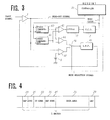
- Fig. 3 shows another embodiment of the present invention which controls the threshold level by a first control means.
- a first phase comparator 40 and a second phase comparator 41 respectively compare the rising edge and the falling edge of a shaped signal which is outputted from a waveform comparator 1 with a read clock outputted from a voltage controlled oscillator 3.
- An adder 42 serves to add the outputs of the first and second phase comparators 40 and 41 to each other.
- the first phase comparator 40, the second phase comparator 41 and the adder 42 are equivalent to the aforesaid phase comparator 2 in Fig. 1 and constitute a phase-clocked loop (PLL) in combination with the filter 13 and the voltage controlled oscillator 3.
- PLL phase-clocked loop
- the output of the voltage controlled oscillator 3 is used as the read clock. If the threshold level becomes higher, as will be apparent from comparison of the shaped signal D with another shaped signal E shown in Fig. 2, the rising edge lags while the falling edge advances. In case the threshold level becomes lower to the contrary, such phenomenon is rendered reverse.
- the threshold level error can be detected by first taking out a difference between the outputs of the first and second phase comparators 40 and 41 by a differential amplifier 44, and then extracting the low-frequency component through a low-pass filter 45.
- the threshold level of the waveform comparator 1 can be controlled by feeding back the error thus obtained.
- the threshold level has a great deviation from its optimal value to such an extent that the pulse duration of the shaped signal varies by a length of one clock pulse or so as compared with the original digital signal, a read error is generated as a result, and the threshold level control comes to be stabilized in a state where the pulse duration of the read-out signal G has a variation of one clock pulse in comparison with that of the original digital signal.
- Such state is defined here as "spurious lock". Although the spurious lock is scarcely induced once the threshold level is controlled to its proper value, it may often occur at the beginning of the control operation.
- the embodiment of Fig. 1 is so operated that the controller 50 changes the mode selection signal to "L" state to place the transfer gate 5 in a high-impedance condition. Since the input terminal of the low-pass filter 9 is connected to a power supply 6 of a voltage V through a resistor 7, the low-pass filter 9 provides an output DC voltage corresponding to the supply voltage V.
- the differential amplifier 10 compares the output of the low-pass filter 8 with the output DC voltage of the low-pass filter 9, and feeds the difference back to the threshold level. Accordingly, the threshold level is so locked that the DC level of the shaped signal becomes a predetermined value.
- a second control means is constituted by the closed loop which controls the threshold level by comparing the low-frequency component of the shaped signal with the DC voltage V.
- the threshold level is not always exactly controlled to its optimal value because the low-frequency component of the information-carrying digital signal does not always retain a fixed voltage.
- the threshold level can be kept at its optimal value by the second control means.
- the repetition signal is termed here a "SYNC signal".
- the threshold level can be kept at its optimal value by the second control means.
- Fig. 4 shows an exemplary format where each sector includes an ID area 22 for recording an address and so forth, and a data area 23 for recording a data signal which carries the information to be recorded.
- the individual areas are separated from each other by a gap 20.
- a SYNC signal 21 is added to the beginning of each area, so that the SYNC signal 21 and the following ID signal or data signal are recorded continuously.
- the controller 50 When reading out the information from such recording medium, the controller 50 initially sets the mode selection signal to "L" state to set the second control means in an active condition. In this stage, the gain of the variable gain amplifier 11 is increased by the mode selection signal so that the threshold-level control loop is ready for fast response. Upon arrival of the SYNC signal 21, the phase-locked loop of the clock extracting circuit 12 and the threshold-level control loop are promptly synchronized so that the predetermined pattern of the SYNC signal 21 is recognized by the controller 50. The controller 50, when recognized the SYNC signal 21, changes the mode selection signal to "H" state so that the threshold level is controlled by the first control means. Thus, a shaped signal of the optimal level can be obtained despite any variation of the low-frequency component in the data signal or ID signal. In this stage, since the variable gain amplifier 11 is switched to a small-gain condition by the mode selection signal, the threshold level control operation is hardly affected by any noise or the like to consequently ensure stable and accurate read of the information.
- the controller 50 set a SYNC detected signal (which has been initially reset) when detects the SYNC signal 21, and reset the SYNC detected signal after reading the following data.
- This known SYNC detected signal can be directly used as the mode selection signal.
- the controller 50 may produce the mode selection signal which is made "H" in response to a first coming SYNC signal after the start of the information reproducing operation.
- the mode selection signal may not be necessary to be controlled in response to the SYNC signal.
- the mode selection signal may be controlled by a timer which shows a time when the operation of the apparatus is stabilized after the start time. Also, the mode selection signal may be controlled in accordance with any other proper manner by the controller 50.
- an information for controlling the mode selection signal may be contained in the input signal of the apparatus.
- Fig. 5 shows a further embodiment of the invention effective for a channel code signal processed by a DC-free modulation system which controls the original of an input signal in such a manner that its DC component becomes a predetermined value.
- a differential amplifier 10 compares the output of a low-pass filter 8, obtained by extracting the low-frequency component of a shaped signal with the output of another low-pass filter 9 obtained by extracting the low-frequency component of a read-out signal to detects a threshold level error in a first control means.
- Another differential amplifier 32 compares the output of the low-pass filter 8 with a fixed voltage V to detects a threshold level error in a second control means.
- the threshold level of a waveform comparator 1 is controlled in accordance with the sum of the output signal from an integrator 30 which integrates the threshold level error detected by the second control means and the threshold level error detected by the first control means.
- Fig. 6 graphically shows exemplary gain characteristics of the control loops in the respective modes.
- a and B represents the gain characteristic of the first control means and that of the second control means, respectively.
- the circuit configuration is so designed that, as shown in Fig. 6, the second control means is dominant in a direct current while the first control means is dominant at a cross-over frequency fo where the open-loop gain of the first control means becomes 0 dB.
- the threshold level is controlled by the first control means in a band from a frequency fc where the gain characteristics A and B cross each other to the frequency fo, so that optimal control of the threshold level can be attained even when the original digital signal contains some frequency component of this band.
- the second control means Since the second control means is dominant in the frequency range below fc, if spurious lock is induced due to some reason in the threshold level control performed by the first control means, there exists no possibility that such state is retained for a long time, because the spurious lock is promptly eliminated by the second control means to eventually resume the proper threshold level.
- the threshold level in shaping the waveform of the input signal can be controlled optimally with reference to a read clock extracted from the input signal even if the original channel code signal is not the one processed by DC-free modulation, and a combination with the threshold level control performed by the second control means realizes solution of the known problem that the threshold-level control loop is prone to cause spurious lock.
Abstract
Description
- The present invention relates to a digital information reproducing apparatus for reading out an information from a digital signal obtained through a band-limited transmission system, and more particularly to an apparatus capable of controlling the threshold level of a waveform shaper so as to correctly read the digital signal.
- For the purpose of transmitting digital signals at a high transfer rate or recording them at a high density, there is often employed recently a technique of digital modulation which transmits or records digital signals within a base band. In such a signal transmission using a base band, it is generally necessary to transmit even the lowest frequency range including a DC component and is further necessary to shape the rounded waveform which is deformed in the transmission line to a proper shape at a predetermined threshold level. However, there exists a problem that an optimal threshold level is drifted because some low frequency noise is prone to mix into the input signal due to temperature drift in a circuit or nonuniformity of a recording medium used. For solving such problem, there is known a conventional method which controls the threshold level to an optimal value for elimination of any harmful influence that results from the drift of the threshold level caused by low frequency noise.
- As regards a channel code signal processed by a DC-free modulation system according to which the DC component of the signal to be transmitted is not modulated, it is possible to attain an optimal threshold level by controlling the threshold level in such a manner that the DC component of the waveform-shaped signal obtained from the transmitted input signal becomes a predetermined value. An exemplary waveform shaper for controlling the threshold level as mentioned above is disclosed in Japanese Patent Application of Laid-open No. 57 (1982)-78611.
- In such a conventional waveform shaper, however, controlled retention of the threshold level at an optimal value is not achievable in case the input is not a channel code signal processed by the DC-free modulation system. For example, in the so-called 2-7 code modulation employed frequently in the recent magnetic storage system and so forth, there occurs variation in the DC component of the modulated channel code signal, and consequently it is impossible to attain optimal control of the threshold level by the method mentioned.
- Also with respect to the channel code signal modulated by some other system than the DC-free modulation, it is still possible to accomplish optimal control of the threshold level by detecting the threshold level error with reference to a read clock extracted from the channel code signal. An exemplary waveform shaper for controlling the threshold level in this manner is disclosed in Japanese Patent Application of Laid-open No. 59 (1984)-113529, wherein the threshold level is controlled in accordance with a difference obtained from the phase difference between the rising edge of the shaped input signal and the read clock and the phase difference between the falling edge and the read clock.
- However, in the method which detects the threshold level error with reference to the read clock as mentioned above, if there occurs a variation in the threshold level in such a manner that the pulse duration changes by a length comparable to the read clock period, the signal with such pulse duration change may be erroneously recognized as the original signal. In such a case, there is induced a state of spurious lock where the threshold level is controlled to an improper value.
- It is an object of the present invention to provide a digital information reproducing apparatus which is capable of controlling the threshold level optimally for shaping the waveform of a modulated channel code signal regardless of whether the modulation system is DC-free or not, and is further capable of averting spurious lock in control of the threshold level.
- In order to accomplish this object, the present invention uses a threshold level control means, for controlling the threshold level when shaping the waveform of an input signal, which comprises a first control means for controlling the threshold level with reference to a read clock extracted from the input signal, and a second control means functioning in cooperation with the first control means and serving to control the threshold level in such a manner that the DC component of the shaped signal obtained after shaping the waveform of the input signal becomes a predetermined value.
- In this constitution, the first control means is capable of optimally controlling the threshold level even if the input signal is the one processed by any modulation system that may cause variation in the DC component, and the second control means is adapted to prevent spurious lock of the first control means.
-
- Fig. 1 is a block diagram of a preferred embodiment of the present invention;
- Fig. 2 is a waveform chart of signals produced in the embodiment of Fig. 1;
- Fig. 3 is a block diagram of another embodiment of the invention;
- Fig. 4 is a conceptual diagram of an exemplary format on a recording medium;
- Fig. 5 is a block diagram of a further embodiment of the invention; and
- Fig. 6 graphically shows the gain characteristic of a threshold-level control loop in the embodiment of Fig. 5.
- This invention is useful both for digital data communication systems and for digital data storage systems, and will be described herein with reference to the latter.
- In Fig. 1, a
waveform comparator 1 is supplied with an input digital signal deformed in waveform through a band-limited transmission system, which may be a communication channel or a recording-reproducing channel. Here a description will be given on a recording-reproducing channel as an example. Thecomparator 1 shapes the waveform of the input signal to produce a shaped signal. Aclock extracting circuit 12 extracts a read clock from the shaped signal. Theclock extracting circuit 12 is composed of a phase-locked loop (PLL) comprising aphase comparator 2, afilter 13 and a voltage controlled oscillator (V.C.O) 3. A D-flip-flop 4 latches the shaped signal synchronously with the read clock. The synchronized read-out signal thus outputted from the D-flip-flop 4 is the same as the original signal recorded on a recording medium. The read-out signal and read clock are sent to a well-knowncontroller 50. Thecontroller 50 produces a mode selection signal for controlling a transfer gate 5. - When a mode selection signal is in its "H" state, the read-out signal is permitted to pass through a transfer gate 5. Low-frequency components are extracted from the shaped signal and the read-out signal respectively through low-
pass filters differential amplifier 10 detects a difference between the two low-frequency components. Avariable gain amplifier 11 amplifies this difference and feeds it back to thecomparator 1 as a threshold level. Thus, the control loop for controlling the threshold level to an optimal value with reference to the read clock constitutes a first control means. - Referring now to the signal waveform chart of Fig. 2, the operation of the first control means will be described in further detail. In this chart, A is a write clock and B is an original digital signal to be recorded synchronously with the clock A. Denoted by C, D, E, F and G are signals obtained at points c, d, e, f and g in Fig. 1, respectively. When the digital signal B is recorded and reproduced, generally the reproduced signal is deformed in waveform as represented by C. A shaped signal D obtained by shaping the waveform of the reproduced signal C at an optimal threshold level S1 thereof comes to have the same waveform as that of the digital signal B. In the
clock extracting circuit 12, a read clock F is extracted from the shaped signal D. The read clock F is substantially opposite in phase to the recording clock A. The read-out signal G produced in the D-flip-flop 4 by synchronizing the shaped signal D with the read clock F is equivalent to the one obtained by delaying the shaped signal D. Consequently, the difference between the outputs of the low-pass filters - However, if the threshold level is S2 which is higher than the optimal threshold level S1, the shaped signal outputted from the
comparator 1 becomes such as represented by E, in which the duty ratio is smaller than that of the digital signal B. When the shaped signal E is synchronized with the clock F in case the threshold level error is not so great as to bring about a read error, the read-out signal G is obtained similarly to the foregoing case where the threshold level is S1. Therefore, the output of the low-pass filter 8 becomes smaller than that of the low-pass filter 9, whereby the threshold level of thecomparator 1 is caused to change in the negative direction. Thus, the threshold level of thecomparator 1 is controlled with negative feedback. - Fig. 3 shows another embodiment of the present invention which controls the threshold level by a first control means. A
first phase comparator 40 and asecond phase comparator 41 respectively compare the rising edge and the falling edge of a shaped signal which is outputted from awaveform comparator 1 with a read clock outputted from a voltage controlledoscillator 3. Anadder 42 serves to add the outputs of the first andsecond phase comparators first phase comparator 40, thesecond phase comparator 41 and theadder 42 are equivalent to theaforesaid phase comparator 2 in Fig. 1 and constitute a phase-clocked loop (PLL) in combination with thefilter 13 and the voltage controlledoscillator 3. Similarly to the case of Fig. 1, the output of the voltage controlledoscillator 3 is used as the read clock. If the threshold level becomes higher, as will be apparent from comparison of the shaped signal D with another shaped signal E shown in Fig. 2, the rising edge lags while the falling edge advances. In case the threshold level becomes lower to the contrary, such phenomenon is rendered reverse. The threshold level error can be detected by first taking out a difference between the outputs of the first andsecond phase comparators differential amplifier 44, and then extracting the low-frequency component through a low-pass filter 45. The threshold level of thewaveform comparator 1 can be controlled by feeding back the error thus obtained. - By referring to the read clock as mentioned above, it becomes possible to attain optimal control of the threshold level if the original of the input signal is a channel code signal processed by some other system than the DC-free modulation system. However, if the threshold level has a great deviation from its optimal value to such an extent that the pulse duration of the shaped signal varies by a length of one clock pulse or so as compared with the original digital signal, a read error is generated as a result, and the threshold level control comes to be stabilized in a state where the pulse duration of the read-out signal G has a variation of one clock pulse in comparison with that of the original digital signal. Such state is defined here as "spurious lock". Although the spurious lock is scarcely induced once the threshold level is controlled to its proper value, it may often occur at the beginning of the control operation.
- For the purpose of preventing the spurious lock, the embodiment of Fig. 1 is so operated that the
controller 50 changes the mode selection signal to "L" state to place the transfer gate 5 in a high-impedance condition. Since the input terminal of the low-pass filter 9 is connected to apower supply 6 of a voltage V through a resistor 7, the low-pass filter 9 provides an output DC voltage corresponding to the supply voltage V. Thedifferential amplifier 10 compares the output of the low-pass filter 8 with the output DC voltage of the low-pass filter 9, and feeds the difference back to the threshold level. Accordingly, the threshold level is so locked that the DC level of the shaped signal becomes a predetermined value. In this case, a second control means is constituted by the closed loop which controls the threshold level by comparing the low-frequency component of the shaped signal with the DC voltage V. Although there exists no possibility that the aforementioned spurious lock is induced under the control of the second control means, the threshold level is not always exactly controlled to its optimal value because the low-frequency component of the information-carrying digital signal does not always retain a fixed voltage. However, in case the recorded digital signal is such that the DC value thereof is constant and none of low-frequency component is contained, the threshold level can be kept at its optimal value by the second control means. - When recording an information by dividing a recording medium into a plurality of sectors, a repetition signal of a predetermined pattern is recorded often at the beginning of the data signal so as to maintain the clock extracting circuit in synchronism. For this reason, the repetition signal is termed here a "SYNC signal". In the SYNC signal portion, the threshold level can be kept at its optimal value by the second control means.
- Fig. 4 shows an exemplary format where each sector includes an
ID area 22 for recording an address and so forth, and adata area 23 for recording a data signal which carries the information to be recorded. The individual areas are separated from each other by agap 20. At the time of recording an ID signal or data signal in such areas, aSYNC signal 21 is added to the beginning of each area, so that theSYNC signal 21 and the following ID signal or data signal are recorded continuously. - When reading out the information from such recording medium, the
controller 50 initially sets the mode selection signal to "L" state to set the second control means in an active condition. In this stage, the gain of thevariable gain amplifier 11 is increased by the mode selection signal so that the threshold-level control loop is ready for fast response. Upon arrival of theSYNC signal 21, the phase-locked loop of theclock extracting circuit 12 and the threshold-level control loop are promptly synchronized so that the predetermined pattern of theSYNC signal 21 is recognized by thecontroller 50. Thecontroller 50, when recognized theSYNC signal 21, changes the mode selection signal to "H" state so that the threshold level is controlled by the first control means. Thus, a shaped signal of the optimal level can be obtained despite any variation of the low-frequency component in the data signal or ID signal. In this stage, since thevariable gain amplifier 11 is switched to a small-gain condition by the mode selection signal, the threshold level control operation is hardly affected by any noise or the like to consequently ensure stable and accurate read of the information. - Incidently, it is known the
controller 50 set a SYNC detected signal (which has been initially reset) when detects theSYNC signal 21, and reset the SYNC detected signal after reading the following data. This known SYNC detected signal can be directly used as the mode selection signal. Alternatively, thecontroller 50 may produce the mode selection signal which is made "H" in response to a first coming SYNC signal after the start of the information reproducing operation. Furthermore, the mode selection signal may not be necessary to be controlled in response to the SYNC signal. The mode selection signal may be controlled by a timer which shows a time when the operation of the apparatus is stabilized after the start time. Also, the mode selection signal may be controlled in accordance with any other proper manner by thecontroller 50. Moreover, an information for controlling the mode selection signal may be contained in the input signal of the apparatus. - Fig. 5 shows a further embodiment of the invention effective for a channel code signal processed by a DC-free modulation system which controls the original of an input signal in such a manner that its DC component becomes a predetermined value. In this diagram, a
differential amplifier 10 compares the output of a low-pass filter 8, obtained by extracting the low-frequency component of a shaped signal with the output of another low-pass filter 9 obtained by extracting the low-frequency component of a read-out signal to detects a threshold level error in a first control means. Anotherdifferential amplifier 32 compares the output of the low-pass filter 8 with a fixed voltage V to detects a threshold level error in a second control means. The threshold level of awaveform comparator 1 is controlled in accordance with the sum of the output signal from anintegrator 30 which integrates the threshold level error detected by the second control means and the threshold level error detected by the first control means. - Fig. 6 graphically shows exemplary gain characteristics of the control loops in the respective modes. In this graph, A and B represents the gain characteristic of the first control means and that of the second control means, respectively. The circuit configuration is so designed that, as shown in Fig. 6, the second control means is dominant in a direct current while the first control means is dominant at a cross-over frequency fo where the open-loop gain of the first control means becomes 0 dB. The threshold level is controlled by the first control means in a band from a frequency fc where the gain characteristics A and B cross each other to the frequency fo, so that optimal control of the threshold level can be attained even when the original digital signal contains some frequency component of this band. Since the second control means is dominant in the frequency range below fc, if spurious lock is induced due to some reason in the threshold level control performed by the first control means, there exists no possibility that such state is retained for a long time, because the spurious lock is promptly eliminated by the second control means to eventually resume the proper threshold level.
- According to the present invention, as described hereinabove, the threshold level in shaping the waveform of the input signal can be controlled optimally with reference to a read clock extracted from the input signal even if the original channel code signal is not the one processed by DC-free modulation, and a combination with the threshold level control performed by the second control means realizes solution of the known problem that the threshold-level control loop is prone to cause spurious lock.
- It is to be understood that the aforementioned drawback of readily inducing spurious lock of the first control means is not inherent in the above-described constitution, and it results essentially from reference to the read clock. Therefore the first control means in the embodiment mentioned is merely illustrative, and it is obvious that the present invention is effective with respect to any other modified constitution as well.
Claims (9)
Applications Claiming Priority (6)
| Application Number | Priority Date | Filing Date | Title |
|---|---|---|---|
| JP26408/86 | 1986-02-07 | ||
| JP61026408A JPH0777385B2 (en) | 1986-02-07 | 1986-02-07 | Digital information playback device |
| JP3232186A JPH0634307B2 (en) | 1986-02-17 | 1986-02-17 | Digital information playback device |
| JP32321/86 | 1986-02-17 | ||
| JP267994/86 | 1986-11-11 | ||
| JP26799486A JPH0682494B2 (en) | 1986-11-11 | 1986-11-11 | Digital information playback device |
Publications (3)
| Publication Number | Publication Date |
|---|---|
| EP0232181A2 true EP0232181A2 (en) | 1987-08-12 |
| EP0232181A3 EP0232181A3 (en) | 1989-03-29 |
| EP0232181B1 EP0232181B1 (en) | 1992-09-16 |
Family
ID=27285389
Family Applications (1)
| Application Number | Title | Priority Date | Filing Date |
|---|---|---|---|
| EP87301048A Expired - Lifetime EP0232181B1 (en) | 1986-02-07 | 1987-02-05 | Digital information reproducing apparatus |
Country Status (4)
| Country | Link |
|---|---|
| US (1) | US4852126A (en) |
| EP (1) | EP0232181B1 (en) |
| KR (1) | KR910000645B1 (en) |
| DE (1) | DE3781698T2 (en) |
Cited By (3)
| Publication number | Priority date | Publication date | Assignee | Title |
|---|---|---|---|---|
| EP0519684A2 (en) * | 1991-06-17 | 1992-12-23 | International Business Machines Corporation | Reading signals for optical storage media |
| EP0606478A1 (en) * | 1991-09-30 | 1994-07-20 | Kabushiki Kaisha Toshiba | Data reproducing apparatus |
| EP0657883A2 (en) * | 1993-12-10 | 1995-06-14 | Canon Kabushiki Kaisha | Information reproducing apparatus and method |
Families Citing this family (13)
| Publication number | Priority date | Publication date | Assignee | Title |
|---|---|---|---|---|
| US5025456A (en) * | 1989-02-02 | 1991-06-18 | At&T Bell Laboratories | Burst mode digital data receiver |
| JPH0812979B2 (en) * | 1989-11-21 | 1996-02-07 | 日本電気株式会社 | Automatic gain control device |
| US5097486A (en) * | 1990-07-31 | 1992-03-17 | Ampex Corporation | Pipelined decision feedback decoder |
| US5146476A (en) * | 1990-12-03 | 1992-09-08 | Reliance Comm/Tec Corporation | High gain amplifier for reception of low level pulse code modulation nonreturn-to-zero signals |
| US5469091A (en) * | 1991-03-25 | 1995-11-21 | Matsushita Electric Industrial Co., Ltd.K | Data slice circuit |
| US5295161A (en) * | 1991-05-10 | 1994-03-15 | International Business Machines Corporation | Fiber optic amplifier with active elements feedback circuit |
| US5179577A (en) * | 1991-06-06 | 1993-01-12 | Digital Equipment Corporation | Dynamic threshold data receiver for local area networks |
| DE69228816T2 (en) * | 1992-10-28 | 1999-08-19 | Cit Alcatel | DC offset correction for direct mix TDMA receivers |
| GB2274759B (en) * | 1993-02-02 | 1996-11-13 | Nokia Mobile Phones Ltd | Correction of D.C offset in received and demodulated radio signals |
| US5389839A (en) * | 1993-03-03 | 1995-02-14 | Motorola, Inc. | Integratable DC blocking circuit |
| JP3937457B2 (en) | 1997-11-13 | 2007-06-27 | セイコーエプソン株式会社 | Semiconductor integrated circuit, operation state detector, and electronic device |
| US6249556B1 (en) * | 1998-05-27 | 2001-06-19 | Intel Corporation | Dynamic thresholding for input receivers |
| JP3502618B2 (en) * | 2001-07-19 | 2004-03-02 | 松下電器産業株式会社 | Phase-locked loop circuit and data reproducing apparatus |
Citations (6)
| Publication number | Priority date | Publication date | Assignee | Title |
|---|---|---|---|---|
| US4191976A (en) * | 1978-09-26 | 1980-03-04 | Data General Corporation | Circuit indicating phase relationship |
| EP0047955A2 (en) * | 1980-09-16 | 1982-03-24 | Kabushiki Kaisha Toshiba | Wave-shaping circuit |
| JPS5778611A (en) * | 1980-10-31 | 1982-05-17 | Matsushita Electric Ind Co Ltd | Digital signal reproducing method |
| JPS595740A (en) * | 1982-06-30 | 1984-01-12 | Mitsubishi Electric Corp | Waveform shaping circuit |
| JPS59113529A (en) * | 1982-12-20 | 1984-06-30 | Nec Corp | Reading out circuit of storage device |
| JPS60260223A (en) * | 1984-06-06 | 1985-12-23 | Matsushita Electric Ind Co Ltd | Automatic slice circuit |
Family Cites Families (7)
| Publication number | Priority date | Publication date | Assignee | Title |
|---|---|---|---|---|
| JPS5125283B1 (en) * | 1971-04-30 | 1976-07-30 | ||
| US4071829A (en) * | 1976-11-09 | 1978-01-31 | Harris Corporation | Coherent phase detector using a frequency discriminator |
| CA1175919A (en) * | 1980-02-20 | 1984-10-09 | Toshitaka Tsuda | Device for discriminating between two values of a signal with dc offset compensation |
| FR2497360A1 (en) * | 1980-12-31 | 1982-07-02 | Schlumberger Prospection | PHASE AND AMPLITUDE MEASUREMENT FOR A DIELECTRIC PROPERTIES LOGGING SYSTEM |
| US4602374A (en) * | 1984-02-27 | 1986-07-22 | Nippon Telegraph & Telephone Public Corporation | Multi-level decision circuit |
| US4619002A (en) * | 1984-07-02 | 1986-10-21 | Motorola, Inc. | Self-calibrating signal strength detector |
| US4625240A (en) * | 1984-07-25 | 1986-11-25 | Eeco, Inc. | Adaptive automatic gain control |
-
1987
- 1987-02-05 US US07/011,916 patent/US4852126A/en not_active Expired - Lifetime
- 1987-02-05 EP EP87301048A patent/EP0232181B1/en not_active Expired - Lifetime
- 1987-02-05 DE DE8787301048T patent/DE3781698T2/en not_active Expired - Fee Related
- 1987-02-07 KR KR1019870000992A patent/KR910000645B1/en not_active IP Right Cessation
Patent Citations (6)
| Publication number | Priority date | Publication date | Assignee | Title |
|---|---|---|---|---|
| US4191976A (en) * | 1978-09-26 | 1980-03-04 | Data General Corporation | Circuit indicating phase relationship |
| EP0047955A2 (en) * | 1980-09-16 | 1982-03-24 | Kabushiki Kaisha Toshiba | Wave-shaping circuit |
| JPS5778611A (en) * | 1980-10-31 | 1982-05-17 | Matsushita Electric Ind Co Ltd | Digital signal reproducing method |
| JPS595740A (en) * | 1982-06-30 | 1984-01-12 | Mitsubishi Electric Corp | Waveform shaping circuit |
| JPS59113529A (en) * | 1982-12-20 | 1984-06-30 | Nec Corp | Reading out circuit of storage device |
| JPS60260223A (en) * | 1984-06-06 | 1985-12-23 | Matsushita Electric Ind Co Ltd | Automatic slice circuit |
Non-Patent Citations (4)
| Title |
|---|
| PATENT ABSTRACTS OF JAPAN vol. 129, no. 129 (E-403)(2186), 14th May 1986; & JP-A-60 260 223 (MATSUSHITA) 23-12-1985 * |
| PATENT ABSTRACTS OF JAPAN vol. 6, no. 162 (P-137)(1040), 25th August 1982; & JP-A-57 078 611 (MATSUSHITA) 17-05-1982 * |
| PATENT ABSTRACTS OF JAPAN vol. 8, no. 237 (P-310)(1674), 30th October 1984; & JP-A-59 113 529 (NIPPON) 30-06-1984 * |
| PATENT ABSTRACTS OF JAPAN vol. 8, no. 84, (E-239)(1521), 18th April 1984; & JP-A-59 005 740 (MITSUBISHI) 12-01-1984 * |
Cited By (7)
| Publication number | Priority date | Publication date | Assignee | Title |
|---|---|---|---|---|
| EP0519684A2 (en) * | 1991-06-17 | 1992-12-23 | International Business Machines Corporation | Reading signals for optical storage media |
| EP0519684A3 (en) * | 1991-06-17 | 1993-03-03 | International Business Machines Corporation | Reading signals for optical storage media |
| EP0606478A1 (en) * | 1991-09-30 | 1994-07-20 | Kabushiki Kaisha Toshiba | Data reproducing apparatus |
| EP0606478A4 (en) * | 1991-09-30 | 1994-08-24 | Toshiba Kk | Data reproducing apparatus. |
| EP0657883A2 (en) * | 1993-12-10 | 1995-06-14 | Canon Kabushiki Kaisha | Information reproducing apparatus and method |
| EP0657883A3 (en) * | 1993-12-10 | 1996-01-10 | Canon Kk | Information reproducing apparatus and method. |
| US5592456A (en) * | 1993-12-10 | 1997-01-07 | Canon Kabushiki Kaisha | Information reproducing apparatus and method |
Also Published As
| Publication number | Publication date |
|---|---|
| US4852126A (en) | 1989-07-25 |
| DE3781698T2 (en) | 1993-02-11 |
| KR910000645B1 (en) | 1991-01-31 |
| EP0232181A3 (en) | 1989-03-29 |
| KR870008306A (en) | 1987-09-25 |
| EP0232181B1 (en) | 1992-09-16 |
| DE3781698D1 (en) | 1992-10-22 |
Similar Documents
| Publication | Publication Date | Title |
|---|---|---|
| EP0232181A2 (en) | Digital information reproducing apparatus | |
| KR100324189B1 (en) | PLL circuit | |
| EP0505253B1 (en) | Read out apparatus for reading out information from magneto-optic disk | |
| US4933959A (en) | Tracking bit synchronizer | |
| US5272730A (en) | Digital phase-locked loop filter | |
| US5193035A (en) | Apparatus and method for phase correction of a clock signal by controlling the variable delaying thereof | |
| EP0395347B1 (en) | Sampling frequency reproduction system | |
| US6078451A (en) | Method and apparatus for adjusting data window phase when retrieving data stored on a recording medium | |
| US4617527A (en) | PU lock acquisition with scan restart upon false lock | |
| US4390801A (en) | Circuit for reproducing a clock signal | |
| US5396479A (en) | Apparatus and method for setting a threshold level to maintain duty cycle in a pulse width modulated optical recording system | |
| JP2661062B2 (en) | Data playback device | |
| US5282185A (en) | Apparatus for generating a data signal at an optimal phase | |
| US5260841A (en) | Clock extracting circuit | |
| US7023636B2 (en) | Information recording/reproducing apparatus | |
| US4803704A (en) | Circuit arrangement for the recognition of impermissable phase errors in a phase locked loop | |
| JPH0682494B2 (en) | Digital information playback device | |
| US5233481A (en) | Magnetic recording and reproducing apparatus | |
| US6006006A (en) | Frame pulse generation apparatus for a video cassette recorder | |
| JP2800772B2 (en) | Clock extraction circuit | |
| JPH02132682A (en) | Data demodulation circuit for disk device | |
| JPH0247653Y2 (en) | ||
| JPH0777385B2 (en) | Digital information playback device | |
| JPH0526264B2 (en) | ||
| JPH031304A (en) | Read control system |
Legal Events
| Date | Code | Title | Description |
|---|---|---|---|
| PUAI | Public reference made under article 153(3) epc to a published international application that has entered the european phase |
Free format text: ORIGINAL CODE: 0009012 |
|
| AK | Designated contracting states |
Kind code of ref document: A2 Designated state(s): DE FR GB |
|
| PUAL | Search report despatched |
Free format text: ORIGINAL CODE: 0009013 |
|
| AK | Designated contracting states |
Kind code of ref document: A3 Designated state(s): DE FR GB |
|
| 17P | Request for examination filed |
Effective date: 19890920 |
|
| 17Q | First examination report despatched |
Effective date: 19910328 |
|
| GRAA | (expected) grant |
Free format text: ORIGINAL CODE: 0009210 |
|
| AK | Designated contracting states |
Kind code of ref document: B1 Designated state(s): DE FR GB |
|
| REF | Corresponds to: |
Ref document number: 3781698 Country of ref document: DE Date of ref document: 19921022 |
|
| ET | Fr: translation filed | ||
| PLBE | No opposition filed within time limit |
Free format text: ORIGINAL CODE: 0009261 |
|
| STAA | Information on the status of an ep patent application or granted ep patent |
Free format text: STATUS: NO OPPOSITION FILED WITHIN TIME LIMIT |
|
| 26N | No opposition filed | ||
| REG | Reference to a national code |
Ref country code: GB Ref legal event code: 746 Effective date: 19950224 |
|
| REG | Reference to a national code |
Ref country code: FR Ref legal event code: D6 |
|
| REG | Reference to a national code |
Ref country code: GB Ref legal event code: IF02 |
|
| PGFP | Annual fee paid to national office [announced via postgrant information from national office to epo] |
Ref country code: GB Payment date: 20050202 Year of fee payment: 19 |
|
| PGFP | Annual fee paid to national office [announced via postgrant information from national office to epo] |
Ref country code: DE Payment date: 20050203 Year of fee payment: 19 |
|
| PGFP | Annual fee paid to national office [announced via postgrant information from national office to epo] |
Ref country code: FR Payment date: 20050208 Year of fee payment: 19 |
|
| PG25 | Lapsed in a contracting state [announced via postgrant information from national office to epo] |
Ref country code: GB Free format text: LAPSE BECAUSE OF NON-PAYMENT OF DUE FEES Effective date: 20060205 |
|
| PG25 | Lapsed in a contracting state [announced via postgrant information from national office to epo] |
Ref country code: DE Free format text: LAPSE BECAUSE OF NON-PAYMENT OF DUE FEES Effective date: 20060901 |
|
| GBPC | Gb: european patent ceased through non-payment of renewal fee |
Effective date: 20060205 |
|
| REG | Reference to a national code |
Ref country code: FR Ref legal event code: ST Effective date: 20061031 |
|
| PG25 | Lapsed in a contracting state [announced via postgrant information from national office to epo] |
Ref country code: FR Free format text: LAPSE BECAUSE OF NON-PAYMENT OF DUE FEES Effective date: 20060228 |