EP0228028A1 - Circuit arrangement for transform coding - Google Patents
Circuit arrangement for transform coding Download PDFInfo
- Publication number
- EP0228028A1 EP0228028A1 EP86117581A EP86117581A EP0228028A1 EP 0228028 A1 EP0228028 A1 EP 0228028A1 EP 86117581 A EP86117581 A EP 86117581A EP 86117581 A EP86117581 A EP 86117581A EP 0228028 A1 EP0228028 A1 EP 0228028A1
- Authority
- EP
- European Patent Office
- Prior art keywords
- circuit arrangement
- transformation
- multiplication
- elements
- arrangement according
- Prior art date
- Legal status (The legal status is an assumption and is not a legal conclusion. Google has not performed a legal analysis and makes no representation as to the accuracy of the status listed.)
- Withdrawn
Links
Images

Classifications
-
- G—PHYSICS
- G06—COMPUTING; CALCULATING OR COUNTING
- G06F—ELECTRIC DIGITAL DATA PROCESSING
- G06F17/00—Digital computing or data processing equipment or methods, specially adapted for specific functions
- G06F17/10—Complex mathematical operations
- G06F17/14—Fourier, Walsh or analogous domain transformations, e.g. Laplace, Hilbert, Karhunen-Loeve, transforms
- G06F17/141—Discrete Fourier transforms
- G06F17/142—Fast Fourier transforms, e.g. using a Cooley-Tukey type algorithm
-
- G—PHYSICS
- G06—COMPUTING; CALCULATING OR COUNTING
- G06F—ELECTRIC DIGITAL DATA PROCESSING
- G06F17/00—Digital computing or data processing equipment or methods, specially adapted for specific functions
- G06F17/10—Complex mathematical operations
- G06F17/14—Fourier, Walsh or analogous domain transformations, e.g. Laplace, Hilbert, Karhunen-Loeve, transforms
- G06F17/147—Discrete orthonormal transforms, e.g. discrete cosine transform, discrete sine transform, and variations therefrom, e.g. modified discrete cosine transform, integer transforms approximating the discrete cosine transform
-
- G—PHYSICS
- G06—COMPUTING; CALCULATING OR COUNTING
- G06F—ELECTRIC DIGITAL DATA PROCESSING
- G06F17/00—Digital computing or data processing equipment or methods, specially adapted for specific functions
- G06F17/10—Complex mathematical operations
- G06F17/16—Matrix or vector computation, e.g. matrix-matrix or matrix-vector multiplication, matrix factorization
-
- H—ELECTRICITY
- H04—ELECTRIC COMMUNICATION TECHNIQUE
- H04N—PICTORIAL COMMUNICATION, e.g. TELEVISION
- H04N19/00—Methods or arrangements for coding, decoding, compressing or decompressing digital video signals
- H04N19/60—Methods or arrangements for coding, decoding, compressing or decompressing digital video signals using transform coding
Definitions
- the outputs of the registers R1 to R (N-1) are connected via further multiplication circuits C1 to C (N-1) and the associated downstream accumulators to a total of N inputs of the multiplexer MUX, the output 2 of which represents the circuit output.
- the multiplication circuits each contain a line memory M 0, x to M N-1, x , in each of which a line of the transformation matrix [T] is stored.
- the output of the line memory is connected to an input of a multiplier M0 to M (N-1), the second input of which represents the input of the multiplication circuit.
- the second transformation network corresponds to the first transformation network; only rows with columns were exchanged in the matrix to be realized.
- 7 shows a possible implementation for the two-dimensional transformation with two identical transformation networks TR1 and TR2. Between the two transformation networks a Transponations appointment MT is turned on, the input of the spectral values of [F x] are supplied to the at its output the transposed values [F x T] emits.
- the mode of operation of the transposition memory can be imagined in such a way that the spectral values F x are written into the memory in columns and after which all spectral values have been calculated are read out from the memory line by line.
- the spectral values result in a vector [F x, 0 ] and a corresponding vector [F 0, y ] is read from the first line.
- the transposed spectral value matrix [F x, y T ] is calculated in this circuit. Deviatingly, all spectral values are written into the transposition memory once in columns and then in rows.
- the circuit arrangement shown in FIG. 7 can be used for all two-dimensional transformations.
Abstract
Description
Die Erfindung betrifft eine Schaltungsanordnung zur Transformationscodierung nach dem Oberbegriff des Patentanspruchs 1.The invention relates to a circuit arrangement for transform coding according to the preamble of
Transformationsverfahren werden hauptsächlich zur Codierung von Bildsignalen angewendet. Diese Verfahren sind in dem Aufsatz "Picture Coding A Review", Proceedings of the IEEE, Vol. 68, No. 3, March 1980, S. 366-406 beschrieben. Bei der Transformationscodierung werden digitalisierte Abtastwerte, die Bildelementen eines Fernsehbildes entsprechen, in Spektralwerte umgesetzt. Hierbei wird versucht, die ursprünglich zur Darstellung eines Bildelementes verwendete Information auf den tatsächlichen Informationsgehalt zu reduzieren. Die Redundanzinformation wird im allgemeinen durch eine Irrelevanzreduktion ergänzt. Spezielle Verfahren zur digitalen Übertragung von Fernsehbildern sind in der DE-OS 33 04 787 und der DE-OS 33 04 835 beschrieben.Transformation methods are mainly used to encode image signals. These methods are described in the article "Picture Coding A Review", Proceedings of the IEEE, Vol. 68, No. 3, March 1980, pp. 366-406. In the case of the transformation coding, digitized samples, which correspond to picture elements of a television picture, are converted into spectral values. An attempt is made to reduce the information originally used to represent a picture element to the actual information content. The redundancy information is generally supplemented by an irrelevance reduction. Special methods for the digital transmission of television pictures are described in DE-OS 33 04 787 and DE-OS 33 04 835.
Die Signale des Fernsehbildes werden bei der Transformation in Spektralwerte umgesetzt, deren Koeffizienten übertragen und auf der Empfangsseite in entsprechende Signalwerte (Luminanz und Chrominanz) rückumgesetzt werden. Da es technologisch noch nicht möglich ist, ganze Fernsehbilder geschlossen zu transformieren, begnügt man sich mit der Transformation und Übertragung von Teilbildern. Die Transformation entspricht der mathematischen Multiplikation einer Matrix mit einem Vektor bzw. der Multiplikation mehrerer Matritzen. Diese Multiplikation muß entsprechend der hohen Datenwortrate der Signalwerte eines Fernsehbildes durchgeführt werden.During the transformation, the signals of the television picture are converted into spectral values, the coefficients of which are transmitted and converted back into corresponding signal values (luminance and chrominance) on the receiving side. Since it is not yet technologically possible to transform entire television images in a closed manner, one is content with the transformation and transmission of partial images. The transformation corresponds to the mathematical multiplication of a matrix with a vector or the multiplication of several matrices. This multiplication must are carried out in accordance with the high data word rate of the signal values of a television picture.
Aufgabe der Erfindung ist es, eine Schaltungsanordnung mit geringem Aufwand für eine Echtzeit-Transformationscodierung anzugeben.The object of the invention is to provide a circuit arrangement with little effort for real-time transformation coding.
Diese Aufgabe wird durch die im Patentanspruch 1 angegebenen Merkmale gelöst.This object is achieved by the features specified in
Vorteilhaft bei der erfindungsgemäßen Schaltungsanordnung ist der geringe Hardwareaufwand. Die Schaltung weist eine regelmäßige Struktur auf, dadurch ist sie integrationsfreundlich und einfach realisierbar. Sie ist bei den unterschiedlichsten Transformationsverfahren anwendbar und sowohl für die Hin- als auch für die Rücktransformation geeignet. Falls die Zeilenspeicher (z.B. ROM,RAM,PROM) von außen programmierbar sind, kann ein universell einsetzbarer integrierter Baustein verwendet werden. Die Schaltungsanordnung ist außerdem einfach kaskadierbar, wodurch auch eine variable Transformationslänge realisierbar ist. In den einzelnen Multiplikationsschaltungen muß je Abtastwert nur eine einzige Multiplikation durchgeführt werden.The low amount of hardware is advantageous in the circuit arrangement according to the invention. The circuit has a regular structure, making it easy to integrate and easy to implement. It can be used in a wide variety of transformation processes and is suitable for both the forward and reverse transformation. If the line memories (e.g. ROM, RAM, PROM) are programmable from the outside, a universally applicable integrated block can be used. The circuit arrangement can also be easily cascaded, as a result of which a variable transformation length can also be implemented. In the individual multiplication circuits, only a single multiplication has to be carried out for each sample value.
Ausführungsbeispiele der Erfindung werden anhand von Figuren näher erläutert.Embodiments of the invention are explained in more detail with reference to figures.
Es zeigen
- Fig. 1 ein Prinzipschaltbild der Schaltungsanordnung zur Transformationscodierung,
- Fig. 2 eine Steuerung für die Schaltungsanordnung nach Fig. 1,
- Fig. 3 die Verwendung eines Lesespeichers als Multiplikator,
- Fig. 4 eine Variante der Schaltungsanordnung zur Trans formationscodierung,
- Fig. 5 eine zweite Variante der Schaltungsanordnung,
- Fig. 6 ein Prinzipschaltbild zur zweidimensionalen Transformationscodierung.
- Fig. 7 eine Variante der Schaltungsanordnung zur zweidimensionalen Transformationscodierung,
- Fig. 8 ein eindimensionales Fernsehteilbild und
- Fig. 9 ein zweidimensionales Fernsehteilbild.
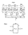
- 1 shows a basic circuit diagram of the circuit arrangement for transformation coding,
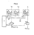
- 2 is a controller for the circuit arrangement of FIG. 1,
- 3 shows the use of a read memory as a multiplier,
- Fig. 4 shows a variant of the circuit arrangement for trans formation coding,
- 5 shows a second variant of the circuit arrangement,
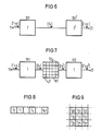
- 6 shows a basic circuit diagram for two-dimensional transformation coding.
- 7 shows a variant of the circuit arrangement for two-dimensional transformation coding,
- Fig. 8 is a one-dimensional television field and
- 9 shows a two-dimensional television field.
Die Schaltungsanordnung zur Transformationscodierung wird zunächst für ein eindimensionales Fernsehteilbild beschrieben, wie es in Fig. 8 dargestellt ist. Als Transformationsmatrix wird die diskrete Cosinustransformation (DCT) verwendet. Mit der Schaltungsanordnung können jedoch auch andere Transformationen wie beispielsweise Slant-, Walsh-, Haar- und M-Transformationen durchgeführt werden.The circuit arrangement for transform coding is first described for a one-dimensional television field, as shown in FIG. 8. The discrete cosine transformation (DCT) is used as the transformation matrix. However, other transformations, such as, for example, Slant, Walsh, Haar and M transformations can also be carried out with the circuit arrangement.
Zunächst sollen die theoretischen Voraussetzungen kurz erläutert werden. Die Spektralwerte F lassen sich berechnen durch die Multiplikation der Transformationsmatrix [T] mit einem Vektor [f], dessen Elemente die Abtastwerte f₀ bis fN-1 eines Fernsehteilbildes darstellen.
(1) [F] = [T] × [f]First, the theoretical requirements are briefly explained. The spectral values F can be calculated by multiplying the transformation matrix [T] by a vector [f], the elements of which represent the samples f₀ to f N-1 of a television field.
(1) [F] = [T] × [f]
Ein einzelner Spektralwert errechnet sich hierbei durch

Für die gesamte Transformation eines Teilbildes gilt somit
Die so gewonnenen Spektralwerte Fi werden ausgesendet. Auf der Empfangsseite werden die Abtastwerte f durch Multiplikation der inversen Matrix mit den Spektralwerten Fi wiedergewonnen.
(4) [f] = [T] ⁻¹ · [F]The spectral values F i obtained in this way are transmitted. On the receiving side, the sample values f are recovered by multiplying the inverse matrix by the spectral values F i .
(4) [f] = [T] ⁻¹ · [F]
Vor der Übertragung werden die Spektralwerte im allgemeinen einem Datenreduktionsverfahren unterzogen. Im Falle einer ortonormalen symmetrischen Transformationsmatrix gilt
(5) [T] ⁻¹ = [T]
so daß zur Hin- und Rücktransformation gleiche Matrix bzw. die gleiche Schaltungsanordnung verwendet werden kann.Before transmission, the spectral values are generally subjected to a data reduction process. In the case of an ortonormal symmetric transformation matrix
(5) [T] ⁻¹ = [T]
so that the same matrix or the same circuit arrangement can be used for the forward and backward transformation.
Weitere theoretische Grundlagen können dem Buch "Fast Transform" von Elliott, Rao, Academic Press, Orlando USA, 1980 entnommen werden.Further theoretical foundations can be found in the book "Fast Transform" by Elliott, Rao, Academic Press, Orlando USA, 1980.
Die Erfindung befaßt sich mit einer Schaltungsanordnung zur Transformationscodierung, wie sie entsprechend Formel 3 durchgeführt wird. Das Prinzipschaltbild der Schaltungsanordnung (Fig. 1) enthält entsprechend der Anzahl N von Elementen fx des Vektors [f] als Laufzeitglieder N-1 Register R1 bis R(N-1), die in Serie geschaltet sind. Ebenso sind N parallele Rechenschaltungen vorgesehen, deren Eingang des ersten Registers R1 ist mit dem Schaltungseingang 1 verbunden und gleichzeitig mit dem Eingang einer nullten Multiplikationsschaltung C₀, deren Ausgang über einen nullten Akumulator A₀ mit einem Eingang eines Multiplexers MUX verbunden ist. Eine Multiplikationsschaltung und ein Akkumulator bilden jeweils eine Rechenschaltung. In derselben Weise sind die Ausgänge der Register R1 bis R(N-1) über weitere Multiplikationsschaltungen C1 bis C(N-1) und den zugehörigen nachgeschalteten Akumulatoren mit weiteren insgesamt N Eingängen des Multiplexers MUX verbunden, dessen Ausgang 2 den Schaltungsausgang darstellt. Die Multiplikationsschaltungen enthalten jeweils einen Zeilenspeicher M0,x bis MN-1,x, in denen jeweils eine Zeile der Transformationsmatrix [T] gespeichert ist. Der Ausgang des Zeilenspeichers ist jeweils mit einem Eingang eines Multiplizierers M0 bis M(N-1) verbunden, dessen zweiter Eingang den Eingang der Multiplikationsschaltung darstellt.The invention relates to a circuit arrangement for transformation coding, as it is carried out according to formula 3. The basic circuit diagram of the circuit arrangement (FIG. 1) contains according to the number N of elements f x of the vector [f] as runtime elements N-1 registers R1 to R (N-1) which are connected in series. Likewise, N parallel computing circuits are provided, the input of the first register R1 is connected to the
Als Multiplizierer und gleichzeitig als Akkumulator kann der Baustein ADSP-1010 A der Fa. Analog Devices, Norwood, Massachusetts, USA, verwendet werden.The ADSP-1010 A module from Analog Devices, Norwood, Massachusetts, USA can be used as a multiplier and at the same time as an accumulator.
Dem Schaltungseingang 1 werden suksessive die Abtastwerte eines Fernsehteilbildes zugeführt. Zunächst liegt der Abtastwert f₀ am Eingang der nullten Multiplikationsschaltung C₀ an, wird mit dem ersten Element t0,0 der Transformationsmatrix multipliziert und in den nullten Akkumulator A0 eingeschrieben, der vorher selbstverständlich gelöscht wurde. Nach einem Taktimpuls liegt derselbe Abtastwert f₀ am Ausgang des ersten Registers R1 an, wird mit dem ersten Element t1,0 der zweiten Zeile der Transformationsmatrix multipliziert und in den ersten Akkumulator A1 eingegeben. Zur selben Zeit wurde der Abtastwert f₁ bereits mit dem zweiten Element t0,1 der ersten Zeile der Transformationsmatrix in der nullten Multiplikationsschaltung multipliziert und zu dem bereits gespeicherten Zahlenwert im nullten Akkumulator A0 hinzuaddiert. Die weiteren Rechenschritte erfolgen analog zu den geschilderten Schritten, wobei mit jedem Taktimpuls das nächste Element einer Zeile der Transformationsmatrix aus dem Zeilenspeicher Z0 abgerufen wird. Nach jeweils N Taktimpulsen liegt am Ausgang des nullten Akkumulators A0 der ersten Spektralwert F₀ an, um über den Multiplexer MUX ausgesendet zu werden. Mit jedem weiteren Taktimpuls liegt an einem weiteren Eingang des Multiplexers ein weiterer Spektralwert an bis nach N Taktimpulsen der letzte Spektralwert FN-1 ausgesendet wird. Die Schaltungsanordnung arbeitet somit kontinuierlich. Mit dem folgenden Taktimpuls wird bereits der erste Spektralwert F₀ des nächsten Teilbildes ausgesendet.The
In jedem Zeilenspeicher müssen nacheinander die einzelnen Elemente (Zahlenwerte) einer Matrixzeile adressiert werden. Dies ist schematisch in Fig. 2 dargestellt. Die Adresssierung erfolgt über eine Steuerung ST. Diese wird besonders einfach, wenn unter derselben über einen Adressenbus AB abgegebenen Adresse jeweils unterschiedliche Elemente einer Matrixzeile aus den Zeilenspeichern ausgelesen werden. In Fig. 2 liegen die Abtastwerte f₀ bis fN-1an den Eingängen der Multiplizierer der Multiplikationsschaltungen C(N-1) bis C0 an. Mit der Adresse N-1 wird im nullten Zeilenspeicher Z0 das letzte Element der ersten Matrixzeile ausgelesen, mit dem letzten Abtastwert fN-1 eines Teilbildes multipliziert und zu den Inhalt des nullten Akkumulators A0 addiert. Am Ausgang des Akkumulators liegt somit der erste Spektralwert F₀ an. Dieser wird über dem Multiplexer MUX ausgesendet und anschließend wird der Inhalt des Akkumulators über einen Rückstellbus RB auf Null gesetzt, damit nach einem weiteren Arbeitstakt das Ergebnis der Multiplikation des ersten Abtastwertes eines neuen Teilbildes mit dem ersten Element der ersten Matrixzeile eingespeichert werden kann. Dieser Vorgang wiederholt sich bei allen Multiplikationsschaltungen und Akkumulatoren, die nacheinander jeweils einen Spektralwert an ihren Ausgang abgeben. Zum selben Zeitpunkt, an dem bereits der erste Spektralwert F₀ am Ausgang des nullten Akkumulators A0 abgegeben wird, liegt am Ausgang des Akkumolators A(N-1) erst das Produkt des ersten Spektralwertes f₀ mit dem nullten Element der letzten Matrixzeile vor.The individual elements (numerical values) of a matrix line must be addressed in succession in each line memory. This is shown schematically in FIG. 2. The addressing takes place via a control ST. This becomes particularly simple when different elements of a matrix line are read from the line memories under the same address given via an address bus AB. 2, the samples f₀ to f N-1 are applied to the inputs of the multipliers of the multiplication circuits C (N-1) to C0. The address N-1 reads out the last element of the first matrix line in the zero line memory Z0, multiplies it with the last sample value f N-1 of a field and adds it to the content of the zero accumulator A0. The first spectral value F₀ is thus present at the output of the accumulator. This is sent out via the multiplexer MUX and then the content of the accumulator is set to zero via a reset bus RB so that after a further work cycle the result of the multiplication of the first sample value of a new field can be stored by the first element of the first matrix line. This process is repeated for all multiplication circuits and accumulators, each of which emits a spectral value in succession at its output. At the same time as the first spectral value F₀ at the output of the zero Accumulator A0 is released, is at the output of the accumulator A (N-1) only the product of the first spectral value f₀ with the zeroth element of the last matrix line.
Als Steuerung kann ein einfacher Binärzähler verwendet werden, dessen Ausgänge den Adressenbus AB bilden, der auch den Multiplexer MUX steuert. Der Rücksetzbus weist N verschiedene Leitungen auf, die nacheinander ein Rücksetzsignal abgeben. Die Codierung der Rücksetzsignale erfolgt über ein Gatternetzwerk aus den Adressen, beispielsweise entsprechend dem Baustein CD 4514 der Fa. RCA, Somerville N.J., USA.A simple binary counter can be used as the control, the outputs of which form the address bus AB, which also controls the multiplexer MUX. The reset bus has N different lines that emit a reset signal in succession. The reset signals are encoded via a gate network from the addresses, for example in accordance with the CD 4514 module from RCA, Somerville N.J., USA.
Als Zeilenspeicher können beliebige Speicherbausteine verwendet werden, die die Geschwindigkeitsanforderungen erfüllen. Ebenso können parallelgeschaltete Schieberegister verwendet werden, in denen die Elemente einer Matrixzeile eingespeichert sind.Any memory modules that meet the speed requirements can be used as the line memory. Shift registers connected in parallel can also be used, in which the elements of a matrix line are stored.
Eine besonders vorteilhafte Ausbildung der Multiplikationsschaltung - hier C0 - ist in Fig. 3 dargestellt. Jede Multiplikationsschaltung enthält eine Lesespeicher (ROM, PROM oder einen entsprechend geladenen RAM), an dessen Adresseneingängen sowohl der Adressenbus AB als auch jeweils ein Abtastwert fx anliegt. Unter der von Adressenbus und Abtastwert gebildeten Gesamtadresse ist ein Zahlenwert gespeichert, der bereits das Produkt des entsprechenden Elementes einer Matrixzeile mit dem Abtastwert entspricht. Dieses Produkt wird am Datenausgang des Lesespeichers abgegeben und dem Akkumulator zugeführt.A particularly advantageous embodiment of the multiplication circuit - here C0 - is shown in FIG. 3. Each multiplication circuit contains a read-only memory (ROM, PROM or a correspondingly loaded RAM), at whose address inputs both the address bus AB and a sample f x are present. A numerical value is stored under the total address formed by the address bus and the sample value, which already corresponds to the product of the corresponding element of a matrix line with the sample value. This product is delivered to the data output of the read memory and fed to the accumulator.
In Fig. 4 ist ein weiteres Ausführungsbeispiel der Schaltungsanordnung dargestellt. Alle Eingänge der Multiplikationsschaltungen C0 bis C(N-1) sind parallel geschaltet und mit dem Schaltungseingang 1 verbunden. Die Ausgänge der Multiplikationsschaltungen sind wieder über Akkumulatoren an Paralleleingänge eines Schieberegisters SR angeschaltet, dessen Ausgang dem Schaltungsausgang 2 entspricht.4 shows a further exemplary embodiment of the circuit arrangement. All inputs of the multiplication circuits C0 to C (N-1) are connected in parallel and connected to the
Alle Multiplikations- und Additionsvorgänge werden parallel ausgeführt. In den Akkumulatoren liegen die Spektralwerte für ein Teilbild gleichzeitig vor. Im Ausführungsbeispiel Fig. 4 werden diese Werte parallel in das Schieberegister SR mit einem Einspeichertakt TE übernommen und seriell mit einem Schiebetakt TS ausgeschoben. Das Schieberegister kann durch Bausteine des Typs SN 5495 A von Texas Instruments aufgebaut werden, bei dem die Daten seriell ausgegeben werden. Durch parallelgeschaltete Schieberegisterketten ist natürlich ebenfalls eine wortparallele Ausgabe möglich. Diese Schaltungsanordnung hat den Vorteil, daß alle Akkumulatoren gleichzeitig gelöscht werden können. Anstelle des Schieberegisters SR kann natürlich auch ein Multiplexer MUX verwendet werden, dessen Eingänge jeweils ein Register als Zwischenspeicher vorgeschaltet ist (Fig. 5). Bei dieser Schaltungsausführung werden die in Fig. 1 am Schaltungseingang liegenden Register zum Datenausgang hin verlagert.All multiplication and addition processes are carried out in parallel. The spectral values for a partial image are simultaneously present in the accumulators. In the exemplary embodiment in FIG. 4, these values are transferred in parallel to the shift register SR with a store cycle T E and are shifted out serially with a shift cycle T S. The shift register can be constructed using Texas Instruments SN 5495 A devices, where the data is output serially. Word-parallel output is of course also possible with shift register chains connected in parallel. This circuit arrangement has the advantage that all the accumulators can be deleted at the same time. Instead of the shift register SR, it is of course also possible to use a multiplexer MUX, the inputs of which are each preceded by a register as a buffer (FIG. 5). In this circuit design, the registers located at the circuit input in FIG. 1 are shifted towards the data output.
Für die zweidimensionale Transformation, wie sie beispielsweise bei einem Fernsehteilbild nach Fig. 9 mit 3 × 3 Abtastwerten fx,y erforderlich ist, gilt
(6) [F] = [T] · [f] · [TT]
Hierbei ist[TT] die transponierte Matrix von [T] .The following applies to the two-dimensional transformation, as is required, for example, in the case of a television field image according to FIG. 9 with 3 × 3 samples f x, y
(6) [F] = [T] · [f] · [T T ]
Here, [T T ] is the transposed matrix of [T].
Eine für diese Transformation geeignete Anordnung ist in Fig. 6 dargestellt. Der Eingang des ersten Transformationsnetzwerkes TR1 ist mit 11 bezeichnet und der Ausgang des Transformationsnetzwerkes ist mit dem Eingang eines zweiten Transformationsnetzwerkes TR1T verbunden, dessen Ausgang mit 21 bezeichnet ist. Die Transformationsnetzwerke sind mit dem bisher beschriebenen Schaltungsanordnungen identisch. Im ersten Transformationsnetzwerk werden zunächst die Zeilen eines Fernsehteilbildes wie bisher mit den Elementen der Transformationsmatrix [T] multipliziert. Für jede Zeile des Fernsehteilbildes ergibt sich ein Spektralwertspektrum [Fx] mit insgesamt N² Spektralwerten. Die einzelnen Spektralwerte werden mit der transformierten Transformationsmatrix [TT] multipliziert, so daß am Ausgang des zweiten Transformationsnetzwerkes eine zweidimensionale Transformation durchgeführt ist. Das zweite Transformationsnetzwerk entspricht dem ersten Transformationsnetzwerk; bei der zu realisierenden Matrix wurden nur Zeilen mit Spalten vertauscht. In Fig. 7 ist eine Realisationsmöglichkeit für die zweidimensionale Transformation mit zwei identischen Transformationsnetzwerken TR1 und TR2 dargestellt. Zwischen beiden Transformationsnetzwerken ist ein Transponationsspeicher MT eingeschaltet, dessen Eingang die Spektralwerte [Fx] zugeführt werden und der an seinem Ausgang die transponierten Werte [Fx T] abgibt. Die Arbeitsweise des Transponationsspeichers kann man sich so vorstellen, daß die Spektralwerte Fx spaltenweise in den Speicher eingeschrieben werden und nach dem sämtliche Spektralwerte errechnet sind, zeilenweise wieder aus dem Speicher ausgelesen werden. Für die erste Spalte ergeben die Spektralwerte einen Vektor [Fx,0] und aus der ersten Zeile wird ein entsprechender Vektor [F0,y] ausgelesen. In dieser Schaltung werden die transponierten Spektralwertmatrix [Fx,y T] errechnet. In den Transponationsspeicher werden abweichend einmal alle Spektralwerte spaltenweise und dann zeilenweise eingeschrieben. Die in Fig. 7 dargestellte Schaltungsanordnung kann für alle zweidimensionalen Transformationen verwendet werden.An arrangement suitable for this transformation is shown in FIG. 6. The input of the first transformation network TR1 is designated 11 and the output of the transformation network is connected to the input of a second transformation network TR1 T , whose output is designated 21. The transformation networks are identical to the circuit arrangements described so far. In the first transformation network, the lines of a television field are first multiplied by the elements of the transformation matrix [T] as before. For each line of the television field there is a spectral value spectrum [F x ] with a total of N² spectral values. The individual spectral values are multiplied by the transformed transformation matrix [T T ], so that a two-dimensional transformation is carried out at the output of the second transformation network. The second transformation network corresponds to the first transformation network; only rows with columns were exchanged in the matrix to be realized. 7 shows a possible implementation for the two-dimensional transformation with two identical transformation networks TR1 and TR2. Between the two transformation networks a Transponationsspeicher MT is turned on, the input of the spectral values of [F x] are supplied to the at its output the transposed values [F x T] emits. The mode of operation of the transposition memory can be imagined in such a way that the spectral values F x are written into the memory in columns and after which all spectral values have been calculated are read out from the memory line by line. For the first column, the spectral values result in a vector [F x, 0 ] and a corresponding vector [F 0, y ] is read from the first line. The transposed spectral value matrix [F x, y T ] is calculated in this circuit. Deviatingly, all spectral values are written into the transposition memory once in columns and then in rows. The circuit arrangement shown in FIG. 7 can be used for all two-dimensional transformations.
Claims (10)
dadurch gekennzeichnet,
daß N parallele Rechenzweige mit jeweils einer Multiplikationsschaltung (C0 bis C(N-1)) und einem nachgeschalteten Akkumulator (A0 bis A(N-1)) vorgesehen sind, daß jeder Multiplikationsschaltung (C0 bis C(N-1) nacheinander die Elemente (fx) des Vektors ([f]) zugeführt werden, die mit gespeicherten zugehörigen Elementen (ti,x; i = 0,1...N-1) einer Matrixzeile multipliziert werden, daß die Produkte der Elemente einer Matrixzeile (ti,x) mit den Elementen (fx) des Vektors ([f]) in dem Akkumulator (Ai) addiert werden und
daß die Spektralwerte (Fi) nacheinander über eine Multiplexeinrichtung (MUX) ausgesendet werden.1. Circuit arrangement for transformation coding, in which spectral values (F) are determined by multiplying a transformation matrix ([T]) comprising N × N elements by a vector representing a sequence of signal values, with multiplication and addition devices,
characterized by
that N parallel computing branches, each with a multiplication circuit (C0 to C (N-1)) and a downstream accumulator (A0 to A (N-1)) are provided, that each multiplication circuit (C0 to C (N-1) successively the elements (f x ) of the vector ([f]) are supplied, which are multiplied by stored associated elements (t i, x ; i = 0.1 ... N-1) of a matrix line, that the products of the elements of a matrix line ( t i, x ) are added to the elements (f x ) of the vector ([f]) in the accumulator (A i ) and
that the spectral values (F i ) are transmitted successively via a multiplex device (MUX).
dadurch gekennzeichnet,
daß eine Reihenschaltung von Laufzeitgliedern (R1,R2...R(N-1)) vorgesehen ist,
daß dem ersten Laufzeitglied und der ersten Multiplikationsschaltung (C0) nacheinander die Elemente (fx) des Vektors ([f]) zugeführt werden
und daß die Eingänge der weiteren Multiplikationsschaltungen (C1,C2,...C(N-1)) jeweils an einen Ausgang der Laufzeitglieder (R1,R2,...R(N-1)) angeschlossen sind.2. Circuit arrangement according to claim 1,
characterized by
that a series connection of delay elements (R1, R2 ... R (N-1)) is provided,
that the elements (f x ) of the vector ([f]) are fed to the first delay element and the first multiplication circuit (C0) one after the other
and that the inputs of the further multiplication circuits (C1, C2, ... C (N-1)) are each connected to an output of the delay elements (R1, R2, ... R (N-1)).
dadurch gekennzeichnet,
daß die Eingänge der Multiplikationsschaltungen parallelgeschaltet sind und daß den Akkumulatoren (A0 bis A(N-1)) als Speicher (R0 bis R(N-1)) Register (R0 bis R(N-1)) nachgeschaltet sind, deren Ausgänge eine Multiplikationseinrichtung (MUX) zugeführt sind.3. Circuit arrangement according to one of the preceding claims,
characterized by
that the inputs of the multiplication circuits are connected in parallel and that the accumulators (A0 to A (N-1)) are connected as memories (R0 to R (N-1)) registers (R0 to R (N-1)), the outputs of which are connected Multiplication device (MUX) are supplied.
dadurch gekennzeichnet,
daß die Ausgänge der Akkumulatoren (A0 bis A(N-1)) mit Paralleleingängen eines Schieberegisters (SR) verbunden sind, das als Multiplexeinrichtung die eingespeicherten Spektralwerte (Fx) ausgibt.4. Circuit arrangement according to claim 3,
characterized by
that the outputs of the accumulators (A0 to A (N-1)) are connected to parallel inputs of a shift register (SR), which outputs the stored spectral values (F x ) as a multiplexing device.
dadurch gekennzeichnet,
daß die Multiplikationsschaltungen (C0 bis C(N-1)) jeweils einen Zeilenspeicher (Z0 bis Z(N-1)), in dem die Elemente (ti,x, i = 0,1...N-1, konstant; x = 0,1...N-1) einer Matrixzeile gespeichert sind, und einen Multiplizierer (M0 bis M (N-1)) enthalten.5. Circuit arrangement according to claim 1,
characterized by
that the multiplication circuits (C0 to C (N-1)) each have a line memory (Z0 to Z (N-1)) in which the elements (t i, x , i = 0.1 ... N-1, constant) ; x = 0.1 ... N-1) of a matrix line are stored and contain a multiplier (M0 to M (N-1)).
dadurch gekennzeichnet,
daß als Zeilenspeicher (Z0 bis Z(N-1)) adressierbare Lesespeicher (ROM) oder ringförmige Schieberegister vorgesehen sind.6. Circuit arrangement according to claim 5,
characterized by
that addressable read-only memories (ROM) or ring-shaped shift registers are provided as line memories (Z0 to Z (N-1)).
dadurch gekennzeichnet,
daß als Multiplikationsschaltung (C0,C1,...) ein Lesespeicher (ROM,PROM) vorgesehen ist, dessen Adresseneingänge mit den Adressenbus (AB) einer Steuerung (ST) verbunden sind, dem das jeweilige Element (fx) des Vektors ([f]) als weiterer Adressenteil zugeführt ist
und daß das Produkt eines Elements des Vektors ([f]) und des zugehörigen Elements (ti,x) der Transformationsmatrixzeile unter der insgesamt anliegenden Adresse ge speichert ist.7. Circuit arrangement according to claim 1,
characterized by
that a read-only memory (ROM, PROM) is provided as the multiplication circuit (C0, C1, ...), the address inputs of which are connected to the address bus (AB) of a controller (ST) to which the respective element (f x ) of the vector ([ f]) is supplied as a further address part
and that the product of an element of the vector ([f]) and the associated element (t i, x ) of the transformation matrix row under the total address ge stores.
dadurch gekennzeichnet,
daß zur zweidimensionalen Transformation die Reihenschaltung einer ersten Transformations-Schaltungsanordnung (TR1), eins Transponationsspeichers (MT) und einer zweiten Transformations-Schaltungsanordnung (TR2) vorgesehen ist, daß in der ersten Transformations-Schaltungsanordnung (TR1) zunächst eine vollständige eindimensionale Transformation durchgeführt wird,
daß die hierbei erhaltenen Produkte (Fx) in den Transponationsspeicher (MT) eingeschrieben werden und daß die transponierten Werte (Fx T) der zweiten Transponations-Schaltungsanordnung (TR2) zugeführt werden.8. Circuit arrangement according to one of the preceding claims,
characterized by
that the series connection of a first transformation circuit arrangement (TR1), a transposition memory (MT) and a second transformation circuit arrangement (TR2) is provided for the two-dimensional transformation, that a complete one-dimensional transformation is first carried out in the first transformation circuit arrangement (TR1),
that the products (F x ) obtained in this way are written into the transposition memory (MT) and that the transposed values (F x T ) are fed to the second transposition circuit arrangement (TR2).
dadurch gekennzeichnet,
daß in den Transponationsspeicher (MT) die Produkte einer vollständigen Transformation abwechselnd spalten- und zeilenweise eingeschrieben werden.9. Circuit arrangement according to claim 8,
characterized by
that the products of a complete transformation are written alternately in columns and rows into the transposition memory (MT).
dadurch gekennzeichnet,
daß die Steuerung (ST) zur Adressierung der Zeilenspeicher (Z0 bis Z(N-1)) oder Lesespeicher (ROM) vorgesehen ist, daß die Steuerung (ST) die Akkumulatoren (A0 bis A(N-1)) nach der Berechnung eines Spektralwertes (Fi,Fx) zurücksetzt und außerdem die Multiplexeinrichtung (MUX,SR) steuert.10. Circuit arrangement according to one of the preceding claims,
characterized by
that the controller (ST) for addressing the line memory (Z0 to Z (N-1)) or read memory (ROM) is provided that the controller (ST) the accumulators (A0 to A (N-1)) after the calculation of a Resets spectral values (F i , F x ) and also controls the multiplexing device (MUX, SR).
Applications Claiming Priority (2)
| Application Number | Priority Date | Filing Date | Title |
|---|---|---|---|
| DE3545357 | 1985-12-20 | ||
| DE3545357 | 1985-12-20 |
Publications (1)
| Publication Number | Publication Date |
|---|---|
| EP0228028A1 true EP0228028A1 (en) | 1987-07-08 |
Family
ID=6289124
Family Applications (1)
| Application Number | Title | Priority Date | Filing Date |
|---|---|---|---|
| EP86117581A Withdrawn EP0228028A1 (en) | 1985-12-20 | 1986-12-17 | Circuit arrangement for transform coding |
Country Status (1)
| Country | Link |
|---|---|
| EP (1) | EP0228028A1 (en) |
Cited By (3)
| Publication number | Priority date | Publication date | Assignee | Title |
|---|---|---|---|---|
| EP0289970A2 (en) * | 1987-05-04 | 1988-11-09 | Polaroid Corporation | Electronic image processing circuit |
| EP0447269A2 (en) * | 1990-03-16 | 1991-09-18 | Fujitsu Limited | An image data processing system |
| FR2670593A1 (en) * | 1990-12-12 | 1992-06-19 | Ricoh Kk | Process allowing conversion between two colour spaces in a 32-bit microprocessor |
Citations (8)
| Publication number | Priority date | Publication date | Assignee | Title |
|---|---|---|---|---|
| US4189748A (en) * | 1977-08-23 | 1980-02-19 | Northrop Corporation | Video bandwidth reduction system using a two-dimensional transformation, and an adaptive filter with error correction |
| US4190861A (en) * | 1976-09-07 | 1980-02-26 | U.S. Philips Corporation | Method and arrangement for redundancy-reducing picture coding |
| US4196448A (en) * | 1978-05-15 | 1980-04-01 | The United States Of America As Represented By The Secretary Of The Navy | TV bandwidth reduction system using a hybrid discrete cosine DPCM |
| US4293920A (en) * | 1979-09-04 | 1981-10-06 | Merola Pasquale A | Two-dimensional transform processor |
| US4385363A (en) * | 1978-12-15 | 1983-05-24 | Compression Labs, Inc. | Discrete cosine transformer |
| GB2141847A (en) * | 1983-05-06 | 1985-01-03 | Seiko Instr & Electronics | Matrix multiplication apparatus for graphic display |
| US4493048A (en) * | 1982-02-26 | 1985-01-08 | Carnegie-Mellon University | Systolic array apparatuses for matrix computations |
| US4553220A (en) * | 1983-05-19 | 1985-11-12 | Gti Corporation | Matrix multiplier with normalized output |
-
1986
- 1986-12-17 EP EP86117581A patent/EP0228028A1/en not_active Withdrawn
Patent Citations (8)
| Publication number | Priority date | Publication date | Assignee | Title |
|---|---|---|---|---|
| US4190861A (en) * | 1976-09-07 | 1980-02-26 | U.S. Philips Corporation | Method and arrangement for redundancy-reducing picture coding |
| US4189748A (en) * | 1977-08-23 | 1980-02-19 | Northrop Corporation | Video bandwidth reduction system using a two-dimensional transformation, and an adaptive filter with error correction |
| US4196448A (en) * | 1978-05-15 | 1980-04-01 | The United States Of America As Represented By The Secretary Of The Navy | TV bandwidth reduction system using a hybrid discrete cosine DPCM |
| US4385363A (en) * | 1978-12-15 | 1983-05-24 | Compression Labs, Inc. | Discrete cosine transformer |
| US4293920A (en) * | 1979-09-04 | 1981-10-06 | Merola Pasquale A | Two-dimensional transform processor |
| US4493048A (en) * | 1982-02-26 | 1985-01-08 | Carnegie-Mellon University | Systolic array apparatuses for matrix computations |
| GB2141847A (en) * | 1983-05-06 | 1985-01-03 | Seiko Instr & Electronics | Matrix multiplication apparatus for graphic display |
| US4553220A (en) * | 1983-05-19 | 1985-11-12 | Gti Corporation | Matrix multiplier with normalized output |
Non-Patent Citations (4)
| Title |
|---|
| AFIPS CONFERENCE PROCEEDINGS ON THE 1982 NATIONAL COMPUTER CONFERENCE, Houston, Texas, 7.-10. Juni 1982, Seiten 225-231; G.A. FRANK et al.: "A systolic processor for signal processing" * |
| ARCHIV FÜR ELEKTRONIK UND ÜBERTRAGUNGSTECHNIK, ELECTRONICS AND COMMUNICATION, Band 31, Nr. 6, Juni 1977, Seiten 217-224, Stuttgart, DE; R. NAWRATH: "Vergleichende Betrachtung von prädiktiven Verfahren und Transformationsmethoden in der Bildkodierung" * |
| IEE PROCEEDINGS SECTIONS A-I, Band 130, Nr. 4, August 1983, Seiten 125-130, Old Woking, Surrey, GB; J.V. McCANNY et al.: "Bit-level systolic array circuit for matrix vector multiplication" * |
| PROCEEDINGS OF THE 1985 INTERNATIONAL CONFERENCE ON PARALLEL PROCESSING, 20.-28. August 1985, Seiten 376-383, IEEE, New York, US; I.V. RAMAKRISHNAN et al.: "An optimal family of matrix multiplication algorithms on linear arrays" * |
Cited By (10)
| Publication number | Priority date | Publication date | Assignee | Title |
|---|---|---|---|---|
| EP0289970A2 (en) * | 1987-05-04 | 1988-11-09 | Polaroid Corporation | Electronic image processing circuit |
| EP0289970A3 (en) * | 1987-05-04 | 1990-09-19 | Polaroid Corporation | Electronic image processing circuit |
| EP0447269A2 (en) * | 1990-03-16 | 1991-09-18 | Fujitsu Limited | An image data processing system |
| EP0740472A2 (en) * | 1990-03-16 | 1996-10-30 | Fujitsu Limited | An image data processing system |
| EP0740472A3 (en) * | 1990-03-16 | 1997-02-12 | Fujitsu Ltd | An image data processing system |
| US5689346A (en) * | 1990-03-16 | 1997-11-18 | Fujitsu Limited | Image data processing system |
| EP0447269B1 (en) * | 1990-03-16 | 2000-05-31 | Fujitsu Limited | An image data processing system |
| EP1022911A1 (en) * | 1990-03-16 | 2000-07-26 | Fujitsu Limited | An image data processing system |
| EP1343329A1 (en) * | 1990-03-16 | 2003-09-10 | Fujitsu Limited | An image data processing system |
| FR2670593A1 (en) * | 1990-12-12 | 1992-06-19 | Ricoh Kk | Process allowing conversion between two colour spaces in a 32-bit microprocessor |
Similar Documents
| Publication | Publication Date | Title |
|---|---|---|
| DE2640140C2 (en) | Method and arrangement for redundancy-reducing image coding | |
| DE2718849C2 (en) | Data processing system for data elements of a matrix of M memory modules and with p processors | |
| DE2640157C2 (en) | Method and arrangement for redundancy-reducing coding of pictures | |
| DE2625973C3 (en) | Method and arrangement for the redundancy-reducing transformation of images | |
| DE1901343C3 (en) | Data processing system for the execution of material invoices | |
| DE2619418A1 (en) | METHOD AND DEVICE FOR CONVERTING A BINARY NUMBER INTO A NUMBER MODULO M | |
| DE2132004A1 (en) | Multiplex information transmission system | |
| DE2628473B2 (en) | Digital convolution filter | |
| DE3632639C2 (en) | Device for high-speed processing of image data by folding | |
| DE4038240A1 (en) | PROCESSOR FOR CARRYING OUT AN ORTHOGONAL TRANSFORMATION | |
| DE2854782C2 (en) | Data processing system and method for replacing a block of data in high-speed storage | |
| DE1774682A1 (en) | Device for visible data reproduction | |
| DE2146982A1 (en) | Programmable digital filter device | |
| DE2644506A1 (en) | CALCULATOR FOR CALCULATING DISCRETE FOURIER TRANSFORMS | |
| DE2506671C3 (en) | Binary data handling network | |
| DE2918692A1 (en) | DIGITAL FILTER | |
| EP0228028A1 (en) | Circuit arrangement for transform coding | |
| DE2451235A1 (en) | CIRCUIT ARRANGEMENT FOR A DIGITAL FILTER | |
| DE4218769A1 (en) | Method and arrangement for forming the sum of a chain of products | |
| DE19637369C2 (en) | Digital signal processor with multiplier and method | |
| DE3304591C2 (en) | Digital adding circuit and use | |
| DE2253746A1 (en) | MODULE SIGNAL PROCESS COMPUTER | |
| DE3634691A1 (en) | DIFFERENTIAL PULSE CODE MODULATOR AND THEIR USE AS A DEMODULATOR | |
| DE2543697C3 (en) | Variable digital filter with high bit rate | |
| DE3331043C2 (en) |
Legal Events
| Date | Code | Title | Description |
|---|---|---|---|
| PUAI | Public reference made under article 153(3) epc to a published international application that has entered the european phase |
Free format text: ORIGINAL CODE: 0009012 |
|
| AK | Designated contracting states |
Kind code of ref document: A1 Designated state(s): AT BE CH DE FR GB IT LI NL |
|
| 17P | Request for examination filed |
Effective date: 19871007 |
|
| 17Q | First examination report despatched |
Effective date: 19891030 |
|
| STAA | Information on the status of an ep patent application or granted ep patent |
Free format text: STATUS: THE APPLICATION HAS BEEN WITHDRAWN |
|
| 18W | Application withdrawn |
Withdrawal date: 19910403 |
|
| R18W | Application withdrawn (corrected) |
Effective date: 19910403 |
|
| RIN1 | Information on inventor provided before grant (corrected) |
Inventor name: GRALLERT, HANS-JOACHIM, DR.-ING. |