EP0220705A2 - Quadriphase phase modulation system - Google Patents
Quadriphase phase modulation system Download PDFInfo
- Publication number
- EP0220705A2 EP0220705A2 EP86114876A EP86114876A EP0220705A2 EP 0220705 A2 EP0220705 A2 EP 0220705A2 EP 86114876 A EP86114876 A EP 86114876A EP 86114876 A EP86114876 A EP 86114876A EP 0220705 A2 EP0220705 A2 EP 0220705A2
- Authority
- EP
- European Patent Office
- Prior art keywords
- waveform
- symbol
- waveforms
- current symbol
- phase modulation
- Prior art date
- Legal status (The legal status is an assumption and is not a legal conclusion. Google has not performed a legal analysis and makes no representation as to the accuracy of the status listed.)
- Granted
Links
Images


Classifications
-
- H—ELECTRICITY
- H04—ELECTRIC COMMUNICATION TECHNIQUE
- H04L—TRANSMISSION OF DIGITAL INFORMATION, e.g. TELEGRAPHIC COMMUNICATION
- H04L25/00—Baseband systems
- H04L25/38—Synchronous or start-stop systems, e.g. for Baudot code
- H04L25/40—Transmitting circuits; Receiving circuits
- H04L25/49—Transmitting circuits; Receiving circuits using code conversion at the transmitter; using predistortion; using insertion of idle bits for obtaining a desired frequency spectrum; using three or more amplitude levels ; Baseband coding techniques specific to data transmission systems
- H04L25/4906—Transmitting circuits; Receiving circuits using code conversion at the transmitter; using predistortion; using insertion of idle bits for obtaining a desired frequency spectrum; using three or more amplitude levels ; Baseband coding techniques specific to data transmission systems using binary codes
- H04L25/4908—Transmitting circuits; Receiving circuits using code conversion at the transmitter; using predistortion; using insertion of idle bits for obtaining a desired frequency spectrum; using three or more amplitude levels ; Baseband coding techniques specific to data transmission systems using binary codes using mBnB codes
Definitions
- the present invention relates to a phase modulation system, and more particularly to a phase modulation system suitable for subscriber transmission.
- phase modulation signals such as the biphase codes (also known as the Walsh codes)
- phase modulation codes include quadriphase phase modulation (QPh) codes, which are also called the complex Walsh codes.
- the QPh codes however, have a wide transmission signal band because of its use of square waves and consequently involve the problem of considerably obstructing other systems by crosstalk. Therefore, by the prior art, the square waveform is band-limited with a high-order low-pass filter, the use of which complicates the circuitry and thereby creates a new problem.
- An object of the present invention is to provide a quadriphase phase modulation system capable of generating phase modulation signals which are narrow in bandwidth without having to use the aforementioned filter for the band-limiting purpose.
- a quadriphase phase modulation system comprises serial to parallel (S/P) converter means for converting serial input data into one-symbol two-bit parallel data; means for generating waveform information corresponding to a bit pattern created by the current symbol of the S/P converter means and a symbol prior to this current symbol; memory means for storing a first waveform determined by the current symbol and the symbol prior to the current symbol and a second waveform determined by the current symbol, and supplying the waveform corresponding to the current symbol in response to the waveform information; and a digital to analog converter for converting signals from this memory means into analog signals.
- S/P serial to parallel
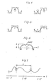
- the conventional QPh code will be described first with reference to FIG. 1. Supposing that the bit rate of a binary code (0 or 1) to be transmitted is 2 f 0 (bits/s) and two bits each (whose combination may be 00, 01, 10 or 11) of this code sequence is one symbol, the symbol can take one of four values.
- FIGS. 2 and 3 illustrate waveforms for use in a QPh modulation system of the invention cleared of the aforementioned disadvantage. The process of providing such waveforms will be described first.
- Each of the conventionally used square waves of FIG.1 is divided into a first to fourth parts on the time axis, and each part of the square wave is transformed into a sine wave as shown in FIG. 4. To simplify the illustration, only waveforms of "00" and "01" are transformed into sine waves.
- phase discontinuities emerge at the points marked with a circle in the drawing. Since such phase discontinuities eventually obstruct the narrowing of the signal bandwidth, further transformation of the waves is required.
- One of the conceivable ways of transformation is to reduce "two peaks" in each sine wave into "one peak” as illustrated in FIG. 5. In doing so, the differential coefficients of the first and second parts, the third and fourth parts, or the second and third parts are equal to each other at the connection point of the two parts. Also, the area of the former half wave is the same as that-of the latter half wave to maintain the D.C. equilibrium.
- FIG. 7 shows how phase discontinuities occur between symbols at the points marked with a circle. Examination of the 16 (2 4 ) kinds of waveforms made by pairs of adjoining symbols here reveals that phase discontinuities occur in eight combinations, identified by waveform numbers 0, 1, 6, 7, A, B, C and D of FIG. 3. The waveforms of FIG. 3 represent only the T/4 portions in the connections between adjoining symbols, and the waveform numbers are expressed sexadecimally. These eight kinds of phase discontinuity can be classified into three types as illustrated in FIGS. 8A to 8C.
- both the first and second connection waveforms (dotted lines) shown in FIG. 8A are sinusoids.
- the second connection waveform is a sinusoid, while the first is the former half of a sinusoid
- the first connection waveform is the former half of a sinusoid while the second is the latter half of a sinusoid.
- connection waveforms are transformed for phase-continuous connection of their respective first and second connection waveforms.
- These wave transformations are achieved by, within the range of
- the waveforms obtained by such transformations are represented by solid lines in FIGS. 8A to 8C.
- the transformed waveform of FIG. 8A is expressed in an equation of the fourth order coinciding with the aforementioned waveform Po(t). That of FIG. 8B is represented by and that of FIG. 8C by In this manner are obtained waveforms for smoothly connecting two consecutive symbols each (hereinafter called connection waveforms).
- the other parts (blank parts) of the waveform shown in FIG. 9 than the connective parts (dotted parts) are determined by the peculiar value of each symbol. It is evident from the waveforms illustrated in FIG. 1 that these waveforms constitute those shown in FIG. 2.
- the waveforms of FIG. 2 are hereinafter considered the basic waveforms. Therefore, consecutive symbols can be represented by the four basic symbols (FIG. 2) determined by an individual symbol and 16 connection waveforms determined by pairs of consecutive symbols.
- FIG. 10 is a table listing the combinations of a basic waveform and a connection waveform determined by two consecutive symbols.
- first and second symbols are "00" and "00" for instance, these two symbols are composed of the connection waveform of sexadecimal 0 and the basic waveform of sexadecimal A.
- symbol "01" is entered following "00" as third symbol, "00" and "01”, according to this table, consist of the connection waveform of sexadecimal 1 and the basic waveform of sexadecimal F.
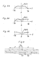
- FIG. 11 is a block diagram illustrating a first embodiment of the present invention for generating the aforementioned waveforms.
- a serial to parallel (S/P) converter 1 converts two-bit series data 11 into two-bit parallel data 12.
- the parallel data constitute symbols.
- a waveform information generator 6 generates information for converting symbols into waveforms in response to the parallel data.
- the generator 6 consists of delay circuits 2 and 3, further comprising flipflops, for delaying the parallel data by one symbol period, and signal lines for directly outputting the parallel data from the S/P converter 1.
- the delayed and undelayed parallel data constitute four-bit patterns of FIG. 10, and are supplied as addresses to a ROM 4.
- the ROM 4 stores 16 waveforms, each consisting of a connecting waveform and a basic waveform corresponding to the outputs listed in FIG. 10, as digital values obtained by sampling these waveforms.
- the ROM 4 outputs one of the waveform data in response to an address of a four-bit pattern.
- a D/A converter 5 converts digital waveforms into analog waveforms.
- Fig. 12 shows a block diagram of a second embodiment of the present invention.
- the memory 4 requires a larger memory capacity because it stores 16 waveforms each of which are generated during T seconds and consists of a basic waveform and a connection waveform.
- a memory 40 used in the second embodiment stores only 16 connection waveforms each of which is generated during seconds and is used for generation of both the connection and basic waveforms.
- the waveform information generator 6 comprises two half-symbol delay circuits 13 and 14 and inverters 15 and 16.
- the inverters 15 and 16 are used to produce exact addresses for basic waveforms.
- the memory 40 requires addresses "1010”, “1111”, “0000” and "0101" to produce the basic waveform numbers A, F, 0 and 5 shown in Fig. 2 by using the connection waveforms as shown in Fig. 10.
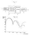
- FIG. 13 is a diagram for explaining how the aforementioned modulated signals are narrowed in bandwidth, wherein the theoretical values of the power spectra of the conventional QPh code (or the complex Welsh code) and the code generated according to the present invention are shown together.
- the solid lines represent the characteristic of the present invention and the dotted lines, that of the prior art.
- the power spectrum of the code of the invention are significantly suppressed in a frequency range of above 2 f o , especially above 4 f 0 .
- the present invention can virtually dispense with a low-pass filter (of a high order) for the band-limiting purpose on the transmitting side, and accordingly has the advantage of permitting substantial simplification of the circuitry composed for digital processing.
Landscapes
- Physics & Mathematics (AREA)
- Spectroscopy & Molecular Physics (AREA)
- Engineering & Computer Science (AREA)
- Computer Networks & Wireless Communication (AREA)
- Signal Processing (AREA)
- Digital Transmission Methods That Use Modulated Carrier Waves (AREA)
- Dc Digital Transmission (AREA)
Abstract
Description
- The present invention relates to a phase modulation system, and more particularly to a phase modulation system suitable for subscriber transmission.
- In base band digital transmission by way of a metallic medium, codes that can be regarded as phase modulation signals, such as the biphase codes (also known as the Walsh codes), are used by the prior art. Such phase modulation codes include quadriphase phase modulation (QPh) codes, which are also called the complex Walsh codes.
- The QPh codes, however, have a wide transmission signal band because of its use of square waves and consequently involve the problem of considerably obstructing other systems by crosstalk. Therefore, by the prior art, the square waveform is band-limited with a high-order low-pass filter, the use of which complicates the circuitry and thereby creates a new problem.
- An object of the present invention, therefore, is to provide a quadriphase phase modulation system capable of generating phase modulation signals which are narrow in bandwidth without having to use the aforementioned filter for the band-limiting purpose.
- A quadriphase phase modulation system according to the invention comprises serial to parallel (S/P) converter means for converting serial input data into one-symbol two-bit parallel data; means for generating waveform information corresponding to a bit pattern created by the current symbol of the S/P converter means and a symbol prior to this current symbol; memory means for storing a first waveform determined by the current symbol and the symbol prior to the current symbol and a second waveform determined by the
current symbol, and supplying the waveform corresponding to the current symbol in response to the waveform information; and a digital to analog converter for converting signals from this memory means into analog signals. - The above and other objects, features and advantages of the present invention will become apparent from the following detailed description when taken with the accompanying drawings in which:
- FIG. 1 is a diagram illustrating a quadriphase phase (QPh) modulation waveform of a square wave by the prior art;
- FIGS. 2 and 3 are diagrams illustrating QPh modulation waveforms for use in the invention;
- FIGS. 4 to 7 and FIGS. 8A to 8C are diagrams for describing the processes to obtain the waveforms for use in the invention;
- FIG. 9 is a diagram illustrating the connective relationship of waveforms for use in the invention;
- FIG. 10 is a table illustrating the relationship between bit patterns and waveforms;
- FIGS. 11 and 12 are block diagrams illustrating first and second embodiments of the invention; and
- FIG. 13 is a diagram illustrating the power spectra of a waveform for use in the invention and a waveform of the prior art.
- To ensure better understanding of the present invention, the conventional QPh code will be described first with reference to FIG. 1. Supposing that the bit rate of a binary code (0 or 1) to be transmitted is 2 f0 (bits/s) and two bits each (whose combination may be 00, 01, 10 or 11) of this code sequence is one symbol, the symbol can take one of four values. One waveform or another in a time T second (= 1/f0) is assigned to each of the four values as shown in FIG. 1, and sent out on a transmission line. In this case, the waveform is square, and the modulation speed is f0 (baud).
- As stated above, however, such a QPh code has a wide signal bandwidth because of its use of square waves, and the use of a band-limiting filter to narrow the bandwidth would entail the problem of complicating the hardware.
- FIGS. 2 and 3 illustrate waveforms for use in a QPh modulation system of the invention cleared of the aforementioned disadvantage. The process of providing such waveforms will be described first.
- Each of the conventionally used square waves of FIG.1 is divided into a first to fourth parts on the time axis, and each part of the square wave is transformed into a sine wave as shown in FIG. 4. To simplify the illustration, only waveforms of "00" and "01" are transformed into sine waves.
- Referring to FIG. 4 wherein the transformed waves are shown, even though sine waves are used, phase discontinuities emerge at the points marked with a circle in the drawing. Since such phase discontinuities eventually obstruct the narrowing of the signal bandwidth, further transformation of the waves is required. One of the conceivable ways of transformation is to reduce "two peaks" in each sine wave into "one peak" as illustrated in FIG. 5. In doing so, the differential coefficients of the first and second parts, the third and fourth parts, or the second and third parts are equal to each other at the connection point of the two parts. Also, the area of the former half wave is the same as that-of the latter half wave to maintain the D.C. equilibrium.
- As an example of such a waveform, one represented by the following fourth order function, illustrated in FIG. 6, can be used.


- Even if the square waves of FIG. 1 are transformed into the shapes illustrated in FIG. 5, there will still emerge phase discontinuities between adjoining symbols. FIG. 7 shows how phase discontinuities occur between symbols at the points marked with a circle. Examination of the 16 (24) kinds of waveforms made by pairs of adjoining symbols here reveals that phase discontinuities occur in eight combinations, identified by
waveform numbers time 0 to time T/4 of the current symbol being regarded as a first connection waveform and that fromtime 0 to time -T/4 of the immediately preceding symbol, as a second connection waveform, both the first and second connection waveforms (dotted lines) shown in FIG. 8A are sinusoids. Further, in the waveform shown in FIG. 8B, the second connection waveform is a sinusoid, while the first is the former half of a sinusoid, and in the waveform shown in FIG. 8C, the first connection waveform is the former half of a sinusoid while the second is the latter half of a sinusoid. - These waveforms of FIGS. 8A to 8C are transformed for phase-continuous connection of their respective first and second connection waveforms. These wave transformations are achieved by, within the range of |t| ≦ T/4 in the figures, making the waveforms continuous at t = ±T/4, the differential coefficients identical at t = ±T/4 and the areas of the waveform of -T/4 ≦ t ≦ 0 and that of 0 ≦ t ≦ T/4 equal (for D.C. balancing). The waveforms obtained by such transformations are represented by solid lines in FIGS. 8A to 8C. The transformed waveform of FIG. 8A is expressed in an equation of the fourth order coinciding with the aforementioned waveform Po(t). That of FIG. 8B is represented by


- Meanwhile, the other parts (blank parts) of the waveform shown in FIG. 9 than the connective parts (dotted parts) are determined by the peculiar value of each symbol. It is evident from the waveforms illustrated in FIG. 1 that these waveforms constitute those shown in FIG. 2. The waveforms of FIG. 2 are hereinafter considered the basic waveforms. Therefore, consecutive symbols can be represented by the four basic symbols (FIG. 2) determined by an individual symbol and 16 connection waveforms determined by pairs of consecutive symbols.
- FIG. 10 is a table listing the combinations of a basic waveform and a connection waveform determined by two consecutive symbols. Referring to FIG. 10, when the first and second symbols are "00" and "00" for instance, these two symbols are composed of the connection waveform of
sexadecimal 0 and the basic waveform of sexadecimal A. Next, when symbol "01" is entered following "00" as third symbol, "00" and "01", according to this table, consist of the connection waveform ofsexadecimal 1 and the basic waveform of sexadecimal F. - FIG. 11 is a block diagram illustrating a first embodiment of the present invention for generating the aforementioned waveforms. Referring to FIG. 11, a serial to parallel (S/P)
converter 1 converts two-bit series data 11 into two-bit parallel data 12. Herein, the parallel data constitute symbols. Awaveform information generator 6 generates information for converting symbols into waveforms in response to the parallel data. Thegenerator 6 consists ofdelay circuits P converter 1. The delayed and undelayed parallel data constitute four-bit patterns of FIG. 10, and are supplied as addresses to aROM 4. TheROM 4 stores 16 waveforms, each consisting of a connecting waveform and a basic waveform corresponding to the outputs listed in FIG. 10, as digital values obtained by sampling these waveforms. TheROM 4 outputs one of the waveform data in response to an address of a four-bit pattern. A D/A converter 5 converts digital waveforms into analog waveforms. - Fig. 12 shows a block diagram of a second embodiment of the present invention. In the first embodiment of FIG. 11, the
memory 4 requires a larger memory capacity because it stores 16 waveforms each of which are generated during T seconds and consists of a basic waveform and a connection waveform. To reduce the memory capacity, amemory 40 used in the second embodiment stores only 16 connection waveforms each of which is generated during seconds and is used for generation of both the connection and basic waveforms. Thewaveform information generator 6 comprises two half-symbol delay circuits 13 and 14 andinverters 15 and 16. - The
inverters 15 and 16 are used to produce exact addresses for basic waveforms. - More specifically, the
memory 40 requires addresses "1010", "1111", "0000" and "0101" to produce the basic waveform numbers A, F, 0 and 5 shown in Fig. 2 by using the connection waveforms as shown in Fig. 10. - However, when the basic waveforms of the symbols "00", "01", "10" and "11" are generated, since the input symbol is the same as the T/2 - delayed symbol as shown in Fig. 9, wrong addresses "0000", "0101", "1010" and "1111" are produced for the symbols "00", "01", "10" and "11", respectively. The comparison of the wrong address with the correct address, for example, "1010" with "0000" shows that the first and third digits are different from each other. Therefore, the
inverters 15 and 16 are necessary to invert the first and third digits to produce a correct address when the basic waveforms are generated. Thememory 40 alternately produces the basic and connection waveforms in response to the addresses supplied from thegenerator 6. - FIG. 13 is a diagram for explaining how the aforementioned modulated signals are narrowed in bandwidth, wherein the theoretical values of the power spectra of the conventional QPh code (or the complex Welsh code) and the code generated according to the present invention are shown together. The solid lines represent the characteristic of the present invention and the dotted lines, that of the prior art. As is evident from the characteristics, the power spectrum of the code of the invention are significantly suppressed in a frequency range of above 2 fo, especially above 4 f0.
- As hitherto described, the present invention can virtually dispense with a low-pass filter (of a high order) for the band-limiting purpose on the transmitting side, and accordingly has the advantage of permitting substantial simplification of the circuitry composed for digital processing.
Claims (5)
Applications Claiming Priority (2)
| Application Number | Priority Date | Filing Date | Title |
|---|---|---|---|
| JP60238605A JPH0685535B2 (en) | 1985-10-26 | 1985-10-26 | Quadrature phase modulation encoder |
| JP238605/85 | 1985-10-26 |
Publications (3)
| Publication Number | Publication Date |
|---|---|
| EP0220705A2 true EP0220705A2 (en) | 1987-05-06 |
| EP0220705A3 EP0220705A3 (en) | 1989-04-05 |
| EP0220705B1 EP0220705B1 (en) | 1993-01-13 |
Family
ID=17032663
Family Applications (1)
| Application Number | Title | Priority Date | Filing Date |
|---|---|---|---|
| EP86114876A Expired - Lifetime EP0220705B1 (en) | 1985-10-26 | 1986-10-27 | Quadriphase phase modulation system |
Country Status (5)
| Country | Link |
|---|---|
| US (1) | US4786882A (en) |
| EP (1) | EP0220705B1 (en) |
| JP (1) | JPH0685535B2 (en) |
| AU (1) | AU586771B2 (en) |
| DE (1) | DE3687507T2 (en) |
Families Citing this family (3)
| Publication number | Priority date | Publication date | Assignee | Title |
|---|---|---|---|---|
| JP2008211766A (en) * | 2007-02-02 | 2008-09-11 | Rohm Co Ltd | Digital modulator, modulation method, fm transmitter employing the same, and electronic device |
| US8948154B2 (en) * | 2010-02-10 | 2015-02-03 | Qualcomm Incorporated | Method and apparatus for sending and receiving a low-complexity transmission in a wireless communication system |
| FR2961988B1 (en) * | 2010-06-25 | 2012-07-27 | Commissariat Energie Atomique | METHOD FOR PHASE MODULATION OF A CARRIER SIGNAL FROM A TRANSMITTER TO A CONTACTLESS TRANSPONDER AND DEVICE FOR IMPLEMENTING THE SAME |
Citations (3)
| Publication number | Priority date | Publication date | Assignee | Title |
|---|---|---|---|---|
| US4339724A (en) * | 1979-05-10 | 1982-07-13 | Kamilo Feher | Filter |
| FR2542535A1 (en) * | 1983-03-11 | 1984-09-14 | Cit Alcatel | Method of synchronous data transmission and system for its implementation |
| WO1984005002A1 (en) * | 1983-06-08 | 1984-12-20 | American Telephone & Telegraph | Multi-function data signal processing method and apparatus |
Family Cites Families (4)
| Publication number | Priority date | Publication date | Assignee | Title |
|---|---|---|---|---|
| IT984397B (en) * | 1973-03-02 | 1974-11-20 | Cselt Centro Studi Lab Telecom | MULTI-LEVEL NONLINEAR ENCODER FOR TRANSMISSION OF NUMERICAL SE GNALS |
| JPS59161157A (en) * | 1983-03-04 | 1984-09-11 | Nippon Telegr & Teleph Corp <Ntt> | Digital processing type phase modulating circuit |
| US4567602A (en) * | 1983-06-13 | 1986-01-28 | Canadian Patents And Development Limited | Correlated signal processor |
| US4644561A (en) * | 1985-03-20 | 1987-02-17 | International Mobile Machines Corp. | Modem for RF subscriber telephone system |
-
1985
- 1985-10-26 JP JP60238605A patent/JPH0685535B2/en not_active Expired - Lifetime
-
1986
- 1986-10-27 EP EP86114876A patent/EP0220705B1/en not_active Expired - Lifetime
- 1986-10-27 US US06/923,470 patent/US4786882A/en not_active Expired - Lifetime
- 1986-10-27 DE DE8686114876T patent/DE3687507T2/en not_active Expired - Fee Related
- 1986-10-27 AU AU64411/86A patent/AU586771B2/en not_active Ceased
Patent Citations (3)
| Publication number | Priority date | Publication date | Assignee | Title |
|---|---|---|---|---|
| US4339724A (en) * | 1979-05-10 | 1982-07-13 | Kamilo Feher | Filter |
| FR2542535A1 (en) * | 1983-03-11 | 1984-09-14 | Cit Alcatel | Method of synchronous data transmission and system for its implementation |
| WO1984005002A1 (en) * | 1983-06-08 | 1984-12-20 | American Telephone & Telegraph | Multi-function data signal processing method and apparatus |
Non-Patent Citations (1)
| Title |
|---|
| IEEE TRANSACTIONS ON MAGNETICS, vol. MAG-15, no. 6, November 1979, pages 1465-1467, IEEE, New York, US; J.A. BIXBY et al.: "Q.P., An improved code for high density digital recording" * |
Also Published As
| Publication number | Publication date |
|---|---|
| EP0220705A3 (en) | 1989-04-05 |
| JPH0685535B2 (en) | 1994-10-26 |
| AU586771B2 (en) | 1989-07-20 |
| DE3687507T2 (en) | 1993-07-29 |
| AU6441186A (en) | 1987-04-30 |
| JPS62100053A (en) | 1987-05-09 |
| US4786882A (en) | 1988-11-22 |
| EP0220705B1 (en) | 1993-01-13 |
| DE3687507D1 (en) | 1993-02-25 |
Similar Documents
| Publication | Publication Date | Title |
|---|---|---|
| EP0776110B1 (en) | Quadrature modulation circuit | |
| KR100313981B1 (en) | Digital signal transmission method and transmitter | |
| US6243422B1 (en) | Waveform shaping method and equipment | |
| EP0716785B1 (en) | An improved rom filter | |
| US5459749A (en) | Multi-level superposed amplitude-modulated baseband signal processor | |
| EP0086091B1 (en) | Apparatus and method for signal processing | |
| US7031403B2 (en) | Phase shift keying modulation including a data converter for converting an input data signal having 3 bits long into two ternary converted data signals | |
| US5321799A (en) | Signalling transition control in a modulated-signal communications system | |
| US5237324A (en) | System and method for producing baseband analog modulation signals | |
| US5745527A (en) | Encoding method for constellation symbols of an RF transmitter | |
| US4674105A (en) | Digital signal processor | |
| EP0112107B1 (en) | Data transmitting-receiving system | |
| US20030147471A1 (en) | Cross correlated trellis coded quatrature modulation transmitter and system | |
| EP0229923B1 (en) | Multilevel qam transmission system introducing supplementary signal points | |
| EP0256700B1 (en) | Apparatus for synthesizing the modulation of a time varying waveform with a data signal | |
| EP0220705A2 (en) | Quadriphase phase modulation system | |
| US4580277A (en) | Digital-based phase shift keying modulator | |
| CA1188759A (en) | Multi-phase digital signal modulation method | |
| EP0191459A2 (en) | Waveform shaping circuit | |
| US4700364A (en) | FSK with continuous phase and continuous slope at bit transitions | |
| US6239666B1 (en) | Uniform amplitude modulator | |
| KR20020060609A (en) | Waveform generator | |
| JP3769384B2 (en) | Digital optical communication signal encoding method, baseband optical transmitter, baseband optical receiver, ASK optical transmitter, and ASK optical receiver | |
| JPH01256851A (en) | Orthogonal modulation system | |
| JPH04168840A (en) | Base band waveform generating circuit for pi/4 shift qpsk modulator |
Legal Events
| Date | Code | Title | Description |
|---|---|---|---|
| PUAI | Public reference made under article 153(3) epc to a published international application that has entered the european phase |
Free format text: ORIGINAL CODE: 0009012 |
|
| 17P | Request for examination filed |
Effective date: 19861031 |
|
| AK | Designated contracting states |
Kind code of ref document: A2 Designated state(s): DE FR GB |
|
| PUAL | Search report despatched |
Free format text: ORIGINAL CODE: 0009013 |
|
| AK | Designated contracting states |
Kind code of ref document: A3 Designated state(s): DE FR GB |
|
| 17Q | First examination report despatched |
Effective date: 19910402 |
|
| GRAA | (expected) grant |
Free format text: ORIGINAL CODE: 0009210 |
|
| AK | Designated contracting states |
Kind code of ref document: B1 Designated state(s): DE FR GB |
|
| REF | Corresponds to: |
Ref document number: 3687507 Country of ref document: DE Date of ref document: 19930225 |
|
| ET | Fr: translation filed | ||
| PLBE | No opposition filed within time limit |
Free format text: ORIGINAL CODE: 0009261 |
|
| STAA | Information on the status of an ep patent application or granted ep patent |
Free format text: STATUS: NO OPPOSITION FILED WITHIN TIME LIMIT |
|
| 26N | No opposition filed | ||
| PGFP | Annual fee paid to national office [announced via postgrant information from national office to epo] |
Ref country code: FR Payment date: 20001010 Year of fee payment: 15 |
|
| PGFP | Annual fee paid to national office [announced via postgrant information from national office to epo] |
Ref country code: DE Payment date: 20001023 Year of fee payment: 15 |
|
| PGFP | Annual fee paid to national office [announced via postgrant information from national office to epo] |
Ref country code: GB Payment date: 20001025 Year of fee payment: 15 |
|
| PG25 | Lapsed in a contracting state [announced via postgrant information from national office to epo] |
Ref country code: GB Free format text: LAPSE BECAUSE OF NON-PAYMENT OF DUE FEES Effective date: 20011027 |
|
| REG | Reference to a national code |
Ref country code: GB Ref legal event code: IF02 |
|
| GBPC | Gb: european patent ceased through non-payment of renewal fee |
Effective date: 20011027 |
|
| PG25 | Lapsed in a contracting state [announced via postgrant information from national office to epo] |
Ref country code: FR Free format text: LAPSE BECAUSE OF NON-PAYMENT OF DUE FEES Effective date: 20020628 |
|
| PG25 | Lapsed in a contracting state [announced via postgrant information from national office to epo] |
Ref country code: DE Free format text: LAPSE BECAUSE OF NON-PAYMENT OF DUE FEES Effective date: 20020702 |
|
| REG | Reference to a national code |
Ref country code: FR Ref legal event code: ST |