EP0219120B1 - Two-wire communication system - Google Patents
Two-wire communication system Download PDFInfo
- Publication number
- EP0219120B1 EP0219120B1 EP86114276A EP86114276A EP0219120B1 EP 0219120 B1 EP0219120 B1 EP 0219120B1 EP 86114276 A EP86114276 A EP 86114276A EP 86114276 A EP86114276 A EP 86114276A EP 0219120 B1 EP0219120 B1 EP 0219120B1
- Authority
- EP
- European Patent Office
- Prior art keywords
- digital
- communication
- process variable
- transmitting unit
- path
- Prior art date
- Legal status (The legal status is an assumption and is not a legal conclusion. Google has not performed a legal analysis and makes no representation as to the accuracy of the status listed.)
- Expired - Lifetime
Links
Images


Classifications
-
- G—PHYSICS
- G08—SIGNALLING
- G08C—TRANSMISSION SYSTEMS FOR MEASURED VALUES, CONTROL OR SIMILAR SIGNALS
- G08C19/00—Electric signal transmission systems
- G08C19/02—Electric signal transmission systems in which the signal transmitted is magnitude of current or voltage
-
- H—ELECTRICITY
- H04—ELECTRIC COMMUNICATION TECHNIQUE
- H04B—TRANSMISSION
- H04B3/00—Line transmission systems
- H04B3/54—Systems for transmission via power distribution lines
- H04B3/548—Systems for transmission via power distribution lines the power on the line being DC
-
- H—ELECTRICITY
- H04—ELECTRIC COMMUNICATION TECHNIQUE
- H04L—TRANSMISSION OF DIGITAL INFORMATION, e.g. TELEGRAPHIC COMMUNICATION
- H04L5/00—Arrangements affording multiple use of the transmission path
- H04L5/14—Two-way operation using the same type of signal, i.e. duplex
- H04L5/16—Half-duplex systems; Simplex/duplex switching; Transmission of break signals non-automatically inverting the direction of transmission
-
- H—ELECTRICITY
- H04—ELECTRIC COMMUNICATION TECHNIQUE
- H04B—TRANSMISSION
- H04B2203/00—Indexing scheme relating to line transmission systems
- H04B2203/54—Aspects of powerline communications not already covered by H04B3/54 and its subgroups
- H04B2203/5404—Methods of transmitting or receiving signals via power distribution lines
- H04B2203/5408—Methods of transmitting or receiving signals via power distribution lines using protocols
-
- H—ELECTRICITY
- H04—ELECTRIC COMMUNICATION TECHNIQUE
- H04B—TRANSMISSION
- H04B2203/00—Indexing scheme relating to line transmission systems
- H04B2203/54—Aspects of powerline communications not already covered by H04B3/54 and its subgroups
- H04B2203/5429—Applications for powerline communications
- H04B2203/5458—Monitor sensor; Alarm systems
-
- H—ELECTRICITY
- H04—ELECTRIC COMMUNICATION TECHNIQUE
- H04B—TRANSMISSION
- H04B2203/00—Indexing scheme relating to line transmission systems
- H04B2203/54—Aspects of powerline communications not already covered by H04B3/54 and its subgroups
- H04B2203/5462—Systems for power line communications
- H04B2203/547—Systems for power line communications via DC power distribution
Definitions
- the present invention relates to a two-wire communication system, and in particular to a communication system suitable to a data communication system or the like between field devices such as terminal process variable transmitters and a control computer of a conventional analog control system used in a plant as well as a present and future digital control system.
- analog data transmission system As a two-wire data transmission or communication system for industrial instruments such as process variable transmitters, conventional analog data transmission system is known.
- the transmitter controls the current in a range of 4 to 20 mA.
- a system as described in Japanese Patent Unexamined Publication No. 85469/83 is known.
- digital data and analog data are alternately transmitted.
- the digital data communication consists of instructions for setting and adjusting transmitter functions sent from a communication unit to transmitters and answers sent from the transmitter to the communication unit. After the analog data transmission state is replaced by the digital data transmission state, a predetermined delay is introduced and then the analog data transmission state is resumed.
- This system is effective when a user adjusts and sets the transmitter function in a communication system of analog data transmission.
- the base state of this system is the analog data transmission state.
- the system for transmitting the process variable signal as digital data from a transmitter to a receiver or a high rank computer is not described.
- the communication unit of the above described system is susceptible to external disturbance or a change in voltage of the power supply because the communication unit is connected in parallel to the power supply, a resistor and a transmitter. Further, the receiver is connected in parallel to a resistor and is different from the communication unit in connection position. This results in lack of uniformity in view of interface to a high rank system in the future.
- An object of the present invention is to provide a communication system which makes possible replacing process variable transmitters in a conventional analog control system or installing process variable transmitters in a new analog control system. This object is achieved with a communication system according to claim 1. Remotely setting and adjusting the transmitter function by the communication unit in the above described system makes it possible for the control computer to control as far as terminals and facilitates digitization of the system.
- the present invention is based upon a concept that the future communication system for the process variable transmitter will be transferred from the analog data transmission system to a digital data transmission system facilitating transmission of higher precision, higher reliability and higher degree of multiplex.
- an analog data transmission state applicable to a conventional analog control system, a digital data transmission state applicable to a digital control system, and a digital communication state making possible remote setting and adjustment from a high rank computer through a communication unit or an interface are provided, and transfer from both transmission states to the digital communication state is permitted.
- Fig. 1 shows a block diagram which is an embodiment of a communication system according to the present invention.
- a process variable transmitter 1 is supplied with power from external power supply 5 through a resistor 4 having a value R L .
- a current I T forms the output signal of the process variable transmitter 1.
- a receiver 2 or a communication unit 3 is connected in parallel to a resistor 4. Under this state, power is supplied from the power supply to the process variable transmitter by using a transmission line 6. At the same time, data communication is conducted between the process variable transmitter and the communication unit, and data are transmitted from the process variable transmitter to the receiver.
- the terminal voltage and output current of the process variable transmitter 1 are represented by V T and I T , respectively.
- the terminal voltage of the resistor (R L ) 4 and the output current of the communication unit 3 are represented by V R and I C , respectively.
- the basic function of each block will now be described.
- the process variable transmitter has constant current characteristics and operates with a current of 4 mA derived through the transmission line.
- the process variable transmitter has analog data transmission function and digital data transmission/receiving function.
- the process variable such as pressure and temperature undergoes compensation processing in a microprocessor included in the process variable transmitter 1.
- the signal thus converted into a suitable form is transmitted as data through the transmission line.
- the process variable transmitter 1 receives digital data transmitted from the communication unit to process the digital data in the above described microprocessor and answers with digital data.
- the receiver is an analog data receiver or a digital data receiver and receives and indicates data. These are selected and set by the user.
- the communication unit has analog data receiving function, digital data transmitting/receiving function, data setting function, data indication function, and function for altering the communication state of the process variable transmitter.
- the whole system shown in Fig. 1 is entirely controlled by the command of the operator through the communication unit. If the system is directly connected to a high rank computer rather than the communication unit in the future, the system is controlled by the high rank computer.
- the analog data transmission state of (1) will now be described by referring to Fig. 2.
- the process variable transmitter transmits analog data by controlling the output current I T in the range of 4 to 20 mA in response to the process variable.
- the output current I T is transmitted through the transmission line and undergoes I/V conversion by the resistor R L to be detected by the receiver.
- Fig. 2 shows I T and V R as functions of time. Values and can be represented as: This state is the same as that of the conventional analog data transmission system and will not be described in detail.
- Data representing one process variable, instruction or answer data is treated as one data block (text) having a series of characters STX, CMD, data and ETX.
- the character STX is a transmission control character for indicating the beginning of the text.
- the character CMD indicates the kind of data.
- Characters D1 to D n are transmission data characters.
- the characters ETX is a transmission control character for indicating the termination of the text.
- Fig. 4 shows the bit structure of each character. This data format conforms to JISC 6220 and its detailed description will be omitted.
- Transmission of digital data is effected by controlling the output currents I T and I C in the process variable transmitter 1 and the communication unit 3, respectively.
- Digital data are transmitted by changing the current in pulse form so that the digital data "1" and "0" may correspond respectively to I min and I max in Fig. 4, for example.
- Such change in current undergoes I/V conversion to be detected as change in voltage by the receiver 2 or the communication unit 3. That is to say, the change in output currents I T or I C is converted into a voltage change via one resistor (R L ) 4 connected in series with the transmission line.
- the change in output current I T is received as a change in V R by the receiver 2 or the communication unit 3.
- a change in output current I C is received as a change in V T by the process variable transmitter 1.
- serial data pulses are obtained.
- the process variable transmitter periodically transmits the process variable as digital data.
- the process variable transmitter transmits digital data by controlling the output current I T in a predetermined current range, say, 4 to 20 mA so that the digital data "1" and "0" may correspond to 4 mA and 20 mA, respectively. Since the minimum operation current necessary for the process variable transmitter is 4 mA, the minimum current of the digital current signal is 4 mA.
- One process variable is transmitted as one data block.
- Data blocks are transmitted one after another at a predetermined transmission period, say, 0.1 sec.
- each data block is received as a change in the terminal voltage V R across the resistor 4 by the receiver 2 or the communication unit 3, resulting in serial data pulses.
- the digital data transmission/receiving function of the process variable transmitter assumes the receiving state between blocks and assumes the transmission state during the transmission of each data block. By using this receiving state, combination with the communication state described later becomes possible.
- the output current I T is fixed at a preset value, say, 4mA.
- the communication unit 3 transmits the function setting and adjusting instruction of the process variable transmitter 1 to the process variable transmitter 1 by using one data block.
- the process variable transmitter 1 also transmits the answer to the above described instruction to the communication unit 3 by using a flow data block.
- the communication unit 3 transmits digital data by controlling the output current in a predetermined current range 0 to I Cl so that digital data "1" and "0" may correspond to 0 mA and I Cl , respectively.
- the instruction data block shown in Fig. 6(a) is received as a change in the terminal voltage V T of the process variable transmitter by the process variable transmitter 1 as shown in Fig.
- the process variable transmitter 1 conducts processing in obedience to the instruction data in the microprocessor thereof. And the process variable transmitter 1 transmits the answer data block as one data block to the communication unit 3 by using the same method as the above described transmission method of the digital data transmission state. Under this communication state, the communication function of the process variable transmitter 1 assumes the receiving state and waits for the instruction from the communication unit. At this time, I T is fixed at a predetermined current value, say, 4 mA.
- FIG. 1 A communication system having the analog data transmission state and a state comprising a combination of the digital data transmissions state and the digital communication state belonging to the three communication states will now be described together with an embodiment of a method for changing over between the two communication states.
- the analog data transmission state is the same as that described before by referring to Fig. 2.
- a method for altering the analog data transmission state will now be described by referring to Figs. 1, 7 and 8. Until time t1 of Fig.
- the process variable transmitter 1 assumes the conventional analog data transmission state, and V T is in a voltage range between and During a predetermined period t c starting from the time t1, a current I Cl is let flow from the communication unit 3 into the resistor 4 to keep V T in a voltage range between V T0 and The relationship between I T and V T under this state and the relationship between I T and V T before t1 will now be described by referring to Fig. 8.
- the process variable transmitter compares the relationship between I T and V T derived as the initial state beforehand with the actual value of V T . When the process variable transmitter has recognized that ⁇ V exceeds the threshold ⁇ V TH for a predetermined period, it terminates the analog data transmission state and resumes the combined state of the digital data transmission and digital communication.
- the transmission period of the process variable transmitter 1 is set by a timer, and process variable data blocks are transmitted in synchronism with the output of the timer.
- the communication unit 3 receives a data block from the process variable transmitter 1 and transmits an instruction data block in synchronism with the termination of the data block from the process variable transmitter 1.
- the communication unit transmits the instruction data block in synchronism with the termination of the data block.
- the interval between data transmitted by the process variable transmitter 1 must be sufficiently longer than the data length transmitted by the communication unit 3.
- the instruction data are transmitted by the method described before with reference to Fig. 6.
- the communication unit 3 transmits an instruction data block
- the communication function of the transmitter assumes the receiving state and the transmitter receives the instruction data block transmitted by the communication unit as described before by reference to Fig. 5.
- the microprocessor included in the process variable transmitter 1 effects processing depending upon the instruction, and transmits the answer data block instead of a process variable data block in synchronism with the transmission period of digital data.
- the transmission method at this time is the same as that described before with reference to Fig. 6. If the instruction from the communication unit 3 is not present thereafter, the process variable transmitter 1 transmits process variable data blocks again with the period T.
- FIG. 10 A method for altering the state comprising a combination of digital data transmission and digital communication will now be described by referring to Fig. 10.
- a state alteration instruction data block is transmitted as the instruction data block of Fig. 9 corresponds to Fig. 10.
- the data transmission/receiving method is the same as that described before by referring to Fig. 9.
- the communication state is transferred to the analog transmission state.
- Figs. 11 and 12 are respectively block diagrams showing the basic configuration of the process variable transmitter 1 and the communication unit 3 satisfying the above described three communication states and function of the embodiment. At first, the configuration and function of the process variable transmitter 1 as well as disposal to the embodiment will now be described by referring to Fig. 11.
- a plurality of process variables such as pressure, differential pressure and temperature are sensed by a composite sensor 7.
- An analog input supplied from the composite sensor 7 is selected by a directive from the input/output selector 10 and is amplified in a programmable amplifier 9 with a gain directed by the input/output selector 10.
- the data which have undergone A/D conversion in an A/D converter undergo compensatory arithmetic processing in an MPU 24 handling the overall operation of the process variable transmitter centering around the calculation and communication processing.
- the date thus arithmetically processed reaches a multiplexer 2 (MPX 2) 17 through an analog output circuit 13 including a D/A converter or through an MPU 24, serial interface, and a digital output circuit 16.
- MPX 2 multiplexer 2
- the MPX 2 17 selects data to be supplied to a current controller 18.
- the current controller 18 including a voltage-to-current conversion circuit controls the output current on the basis of the input.
- the digital input circuit 19 receives digital data transmitted from the communication unit 3 and supplies the digital data to a serial interface of an MPU 24.
- the input/output selector 10 functions to latch the directive from the MPU and output it.
- An EPROM 25 stores the characteristics data and program of compensation calculation therein.
- a timer 26 provides a predetermined operation period.
- the MPU 24 supplies data to the analog output circuit, and selects D2 as the input to the MPX 2 17 through the input/output selector.
- the change ⁇ V in terminal voltage of the process variable transmitter as shown in Figs. 7 and 8 is measured by periodically selecting an A4 input of the MPX 1 8 and applying A/D conversion to V T .
- the MPU 24 sends out data through the serial interface thereof and selects D1 as the input of the MPX 2 17 via the input/output selector 10.
- the directive from the operator is taken into an MPU 34 through a keyboard 38.
- the data constructed by the MPU on the basis of the directive arrive at a current controller 27 through the serial data interface of the MPU 34 and a digital output circuit 32.
- the current controller 27 including a voltage-to-current converter circuit controls the output current in response to its input.
- a digital input circuit 30 receives the digital data transmitted from the process variable transmitter and supplies its output to the serial interface of the MPU 34.
- An A/D converter 37 is supplied with the terminal voltage across the resistor 4 caused by the analog data transmitted from the process variable transmitter 1 and supplies the converted digital data to the MPU 34.
- a ROM 36 stores program therein and a timer 35 provides a predetermined operation period.
- An indicator 39 displays input data supplied from the operator and data transmitted from the process variable transmitter 1.
- the MPU 34 receives data through the A/D converter 37 and the timer 35 provides the receiving period.
- the process variable transmitter 1 assumes the digital data transmission state
- the MPU 34 receives data through the digital input circuit 30.
- the process variable transmitter 1 assumes the digital communication state
- data are sent out through the digital output circuit 32, and the answer data are received through the digital input circuit 30.
- the lead “Tx enable” is usually kept at the low level.
- the period t c is given by the timer.
- FIG. 13 a high rank system is connected to the process variable transmitter through an interface having the transmission/receiving function similar to that of the communication unit 3.
- Fig. 14 shows a system having a plurality of process variable transmitters connected to a two-wire transmission line in parallel. In this system, multiplex operation becomes possible under the digital data transmission state by applying the time division scheme to the transmission period shown in Fig. 5 and adding the address of each transmitter to the process variable data block.
- the process variable transmitter using the present two-wire communication method can be used for replacement in the conventional analog control system and can be easily adapted to the future digital control system. Further, in the conventional analog control system as well, the process variable transmitter can be remotely set and adjusted by altering the communication state. Since the communication unit is connected in parallel to the resistor, the data reception by the communication unit is not susceptible to variation in supply voltage and external disturbance. And both analog data and digital data can be received. If the signal produced when the state is transferred from the analog data transmission state to another state is a pulse signal, there is a possibility of erroneous operation due to disturbance noise. In the present system as shown in Figs. 7 and 8, however, there is not much possibility of erroneous operation. If the two-wire multiplexing as shown in Fig. 14 is used, the wiring process can be simplified and the cost can be reduced.
- the process variable transmitter according to the communication system of the present invention can be used in the conventional analog control system.
- the process variable transmitter can be easily maintained by using the digital communication state.
- the cost when the system is developed can be reduced.
- the digital data transmission state and digital communication state it is possible in the digital control system to collect data from all field terminal devices such as process variable transmitters to a central supervision room and supervise and manage the collected data there, resulting in an efficient digital control system.
- the process variable transmitter according to the communication system of the present invention is effective to communication whereby the output signal is derived while power is being supplied to a sensor.
Description
- The present invention relates to a two-wire communication system, and in particular to a communication system suitable to a data communication system or the like between field devices such as terminal process variable transmitters and a control computer of a conventional analog control system used in a plant as well as a present and future digital control system.
- As a two-wire data transmission or communication system for industrial instruments such as process variable transmitters, conventional analog data transmission system is known. In the analog data transmission system, the transmitter controls the current in a range of 4 to 20 mA. In addition to such a conventional analog data transmission system, a system as described in Japanese Patent Unexamined Publication No. 85469/83 is known. In that system, digital data and analog data are alternately transmitted. The digital data communication consists of instructions for setting and adjusting transmitter functions sent from a communication unit to transmitters and answers sent from the transmitter to the communication unit. After the analog data transmission state is replaced by the digital data transmission state, a predetermined delay is introduced and then the analog data transmission state is resumed. This system is effective when a user adjusts and sets the transmitter function in a communication system of analog data transmission. However, the base state of this system is the analog data transmission state. And the system for transmitting the process variable signal as digital data from a transmitter to a receiver or a high rank computer is not described. In addition, the communication unit of the above described system is susceptible to external disturbance or a change in voltage of the power supply because the communication unit is connected in parallel to the power supply, a resistor and a transmitter. Further, the receiver is connected in parallel to a resistor and is different from the communication unit in connection position. This results in lack of uniformity in view of interface to a high rank system in the future.
- An object of the present invention is to provide a communication system which makes possible replacing process variable transmitters in a conventional analog control system or installing process variable transmitters in a new analog control system. This object is achieved with a communication system according to claim 1. Remotely setting and adjusting the transmitter function by the communication unit in the above described system makes it possible for the control computer to control as far as terminals and facilitates digitization of the system.
- The present invention is based upon a concept that the future communication system for the process variable transmitter will be transferred from the analog data transmission system to a digital data transmission system facilitating transmission of higher precision, higher reliability and higher degree of multiplex. In accordance with the present invention, an analog data transmission state applicable to a conventional analog control system, a digital data transmission state applicable to a digital control system, and a digital communication state making possible remote setting and adjustment from a high rank computer through a communication unit or an interface are provided, and transfer from both transmission states to the digital communication state is permitted.
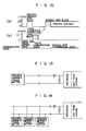
- Fig. 1 shows a block diagram illustrating an embodiment of the present invention.
- Fig. 2 shows transmitted and received waveforms in the analog data transmission state.
- Fig. 3 shows the configuration of a digital data block.
- Fig. 4 shows the bit configuration of characters constituting the data block of Fig. 3.
- Fig. 5 shows transmitted and received waveforms of the digital data transmission state and the state of transmitter communication function.
- Fig. 6 shows transmitted and received waveforms in the digital communication state.
- Fig. 7 shows transmitted and received waveforms for illustrating the method whereby the analog data transmission state is altered.
- Fig. 8 shows the relationship between IT and VT.
- Fig. 9 shows transmitted waveforms in a state comprising a combination of the digital data transmission state and the digital communication state.
- Fig. 10 shows transmitted waveforms for illustrating a method whereby the state of Fig. 9 is altered to the analog data transmission state.
- Fig. 11 shows the functional block diagram of a process variable transmitter for illustrating an embodiment of the present invention.
- Fig. 12 shows the functional block diagram of a communication unit for illustrating an embodiment of the present invention.
- Fig. 13 shows a block diagram for illustrating the connection between a process variable transmitter and a high rank system as a developed form utilizing the present invention.
- Fig. 14 shows a block diagram for illustrating the multiplexing of the two-wire data transmission as a developed form utilizing the digital data transmission state of the present invention.
- An embodiment of the present invention will now be described by referring to drawings. Fig. 1 shows a block diagram which is an embodiment of a communication system according to the present invention. A process variable transmitter 1 is supplied with power from
external power supply 5 through aresistor 4 having a value RL. A current IT forms the output signal of the process variable transmitter 1. Areceiver 2 or a communication unit 3 is connected in parallel to aresistor 4. Under this state, power is supplied from the power supply to the process variable transmitter by using atransmission line 6. At the same time, data communication is conducted between the process variable transmitter and the communication unit, and data are transmitted from the process variable transmitter to the receiver. In Fig. 1, the terminal voltage and output current of the process variable transmitter 1 are represented by VT and IT, respectively. The terminal voltage of the resistor (RL) 4 and the output current of the communication unit 3 are represented by VR and IC, respectively. The basic function of each block will now be described. At first, the process variable transmitter has constant current characteristics and operates with a current of 4 mA derived through the transmission line. And the process variable transmitter has analog data transmission function and digital data transmission/receiving function. The process variable such as pressure and temperature undergoes compensation processing in a microprocessor included in the process variable transmitter 1. The signal thus converted into a suitable form is transmitted as data through the transmission line. Further, the process variable transmitter 1 receives digital data transmitted from the communication unit to process the digital data in the above described microprocessor and answers with digital data. The receiver is an analog data receiver or a digital data receiver and receives and indicates data. These are selected and set by the user. The communication unit has analog data receiving function, digital data transmitting/receiving function, data setting function, data indication function, and function for altering the communication state of the process variable transmitter. The whole system shown in Fig. 1 is entirely controlled by the command of the operator through the communication unit. If the system is directly connected to a high rank computer rather than the communication unit in the future, the system is controlled by the high rank computer. - In view of communication function, there are three kinds of communication state:
- (1) Analog transmission state by means of 4-20 mA DC from the process variable transmitter to the receiver.
- (2) Digital transmission state by means of serial pulses from the variable transmitter to the receiver.
- (3) Digital communication state by means of serial pulses between the process variable transmitter and the communication unit.
- These three kinds of communication state will now be described by referring to Figs. 1 to 6. At first, the analog data transmission state of (1) will now be described by referring to Fig. 2. Under this state, the process variable transmitter transmits analog data by controlling the output current IT in the range of 4 to 20 mA in response to the process variable. The output current IT is transmitted through the transmission line and undergoes I/V conversion by the resistor RL to be detected by the receiver. Fig. 2 shows IT and VR as functions of time. Values

and
can be represented as:
This state is the same as that of the conventional analog data transmission system and will not be described in detail. - Prior to describing the digital data transmission state of (2) and the digital communication state of (3), the data structure of digital data used in the states of (2) and (3) will now be described by referring to Figs. 3 and 4. Data representing one process variable, instruction or answer data is treated as one data block (text) having a series of characters STX, CMD, data and ETX. The character STX is a transmission control character for indicating the beginning of the text. The character CMD indicates the kind of data. Characters D₁ to Dn are transmission data characters. The characters ETX is a transmission control character for indicating the termination of the text. Fig. 4 shows the bit structure of each character. This data format conforms to JISC 6220 and its detailed description will be omitted. The transmission method of digital data will now be described by referring to Figs. 1 and 4. Transmission of digital data is effected by controlling the output currents IT and IC in the process variable transmitter 1 and the communication unit 3, respectively. Digital data are transmitted by changing the current in pulse form so that the digital data "1" and "0" may correspond respectively to Imin and Imax in Fig. 4, for example. Such change in current undergoes I/V conversion to be detected as change in voltage by the
receiver 2 or the communication unit 3. That is to say, the change in output currents IT or IC is converted into a voltage change via one resistor (RL) 4 connected in series with the transmission line. The change in output current IT is received as a change in VR by thereceiver 2 or the communication unit 3. And a change in output current IC is received as a change in VT by the process variable transmitter 1. As a result, serial data pulses are obtained. - By using the above described basic digital data structure and transmission/receiving method, digital data transmission and digital data communication are conducted. The digital data transmission state will now be described in detail by referring to Fig. 5. Under this state, the process variable transmitter periodically transmits the process variable as digital data. As shown in Fig. 5(a), the process variable transmitter transmits digital data by controlling the output current IT in a predetermined current range, say, 4 to 20 mA so that the digital data "1" and "0" may correspond to 4 mA and 20 mA, respectively. Since the minimum operation current necessary for the process variable transmitter is 4 mA, the minimum current of the digital current signal is 4 mA. One process variable is transmitted as one data block. Data blocks are transmitted one after another at a predetermined transmission period, say, 0.1 sec. As shown in Fig. 5(b), each data block is received as a change in the terminal voltage VR across the
resistor 4 by thereceiver 2 or the communication unit 3, resulting in serial data pulses. As shown in Fig. 5(a), the digital data transmission/receiving function of the process variable transmitter assumes the receiving state between blocks and assumes the transmission state during the transmission of each data block. By using this receiving state, combination with the communication state described later becomes possible. In the receiving state, the output current IT is fixed at a preset value, say, 4mA. - The digital communication state will now be described by referring to Figs. 1 and 6. Under the digital communication state, the communication unit 3 transmits the function setting and adjusting instruction of the process variable transmitter 1 to the process variable transmitter 1 by using one data block. Under the digital communication state, the process variable transmitter 1 also transmits the answer to the above described instruction to the communication unit 3 by using a flow data block. The communication unit 3 transmits digital data by controlling the output current in a predetermined
current range 0 to ICl so that digital data "1" and "0" may correspond to 0 mA and ICl, respectively. The instruction data block shown in Fig. 6(a) is received as a change in the terminal voltage VT of the process variable transmitter by the process variable transmitter 1 as shown in Fig. 6(b), resulting in serial data pulses. The process variable transmitter 1 conducts processing in obedience to the instruction data in the microprocessor thereof. And the process variable transmitter 1 transmits the answer data block as one data block to the communication unit 3 by using the same method as the above described transmission method of the digital data transmission state. Under this communication state, the communication function of the process variable transmitter 1 assumes the receiving state and waits for the instruction from the communication unit. At this time, IT is fixed at a predetermined current value, say, 4 mA. - Three communication states have heretofore been described. A communication system having the analog data transmission state and a state comprising a combination of the digital data transmissions state and the digital communication state belonging to the three communication states will now be described together with an embodiment of a method for changing over between the two communication states. At first, the analog data transmission state is the same as that described before by referring to Fig. 2. A method for altering the analog data transmission state will now be described by referring to Figs. 1, 7 and 8. Until time t₁ of Fig. 7, the process variable transmitter 1 assumes the conventional analog data transmission state, and VT is in a voltage range between

and
During a predetermined period tc starting from the time t₁, a current ICl is let flow from the communication unit 3 into theresistor 4 to keep VT in a voltage range between VT0 and
The relationship between IT and VT under this state and the relationship between IT and VT before t₁ will now be described by referring to Fig. 8. When t < t₁, the relationship between IT and VT is represented by a straight line (a) denoted by IC = 0 mA. When t₁ < t < t₂, the relationship between IT and VT is represented by a straight line (b) denoted by IC = ICl. That is to say, a voltage difference
- The state comprising a combination of the digital data transmission and digital communication will now be described by referring to Fig. 9. As shown in (a) and (b) of Fig. 9, the transmission period of the process variable transmitter 1 is set by a timer, and process variable data blocks are transmitted in synchronism with the output of the timer. When the communication unit 3 is to transmit the instruction, the communication unit 3 receives a data block from the process variable transmitter 1 and transmits an instruction data block in synchronism with the termination of the data block from the process variable transmitter 1. There are various synchronization methods for assuring that the instruction data block reaches the process variable transmitter without being confused with the process variable data block. In the present system, however, the communication unit transmits the instruction data block in synchronism with the termination of the data block. In the present system, therefore, the interval between data transmitted by the process variable transmitter 1 must be sufficiently longer than the data length transmitted by the communication unit 3. At this time, the instruction data are transmitted by the method described before with reference to Fig. 6. When the communication unit 3 transmits an instruction data block, the communication function of the transmitter assumes the receiving state and the transmitter receives the instruction data block transmitted by the communication unit as described before by reference to Fig. 5. The microprocessor included in the process variable transmitter 1 effects processing depending upon the instruction, and transmits the answer data block instead of a process variable data block in synchronism with the transmission period of digital data. The transmission method at this time is the same as that described before with reference to Fig. 6. If the instruction from the communication unit 3 is not present thereafter, the process variable transmitter 1 transmits process variable data blocks again with the period T.
- A method for altering the state comprising a combination of digital data transmission and digital communication will now be described by referring to Fig. 10. The case where a state alteration instruction data block is transmitted as the instruction data block of Fig. 9 corresponds to Fig. 10. The data transmission/receiving method is the same as that described before by referring to Fig. 9. After the process variable transmitter 1 has answered to the communication unit 3, the communication state is transferred to the analog transmission state.
- Figs. 11 and 12 are respectively block diagrams showing the basic configuration of the process variable transmitter 1 and the communication unit 3 satisfying the above described three communication states and function of the embodiment. At first, the configuration and function of the process variable transmitter 1 as well as disposal to the embodiment will now be described by referring to Fig. 11.
- A plurality of process variables such as pressure, differential pressure and temperature are sensed by a composite sensor 7. An analog input supplied from the composite sensor 7 is selected by a directive from the input/
output selector 10 and is amplified in a programmable amplifier 9 with a gain directed by the input/output selector 10. The data which have undergone A/D conversion in an A/D converter undergo compensatory arithmetic processing in anMPU 24 handling the overall operation of the process variable transmitter centering around the calculation and communication processing. The date thus arithmetically processed reaches a multiplexer 2 (MPX 2) 17 through ananalog output circuit 13 including a D/A converter or through anMPU 24, serial interface, and adigital output circuit 16. Upon the directive of the input/output selector, theMPX 2 17 selects data to be supplied to acurrent controller 18. Thecurrent controller 18 including a voltage-to-current conversion circuit controls the output current on the basis of the input. Thedigital input circuit 19 receives digital data transmitted from the communication unit 3 and supplies the digital data to a serial interface of anMPU 24. The input/output selector 10 functions to latch the directive from the MPU and output it. AnEPROM 25 stores the characteristics data and program of compensation calculation therein. Atimer 26 provides a predetermined operation period. - Under the analog data transmission state, the
MPU 24 supplies data to the analog output circuit, and selects D2 as the input to theMPX 2 17 through the input/output selector. The change △V in terminal voltage of the process variable transmitter as shown in Figs. 7 and 8 is measured by periodically selecting an A4 input of the MPX 1 8 and applying A/D conversion to VT. Under the digital data transmission state, theMPU 24 sends out data through the serial interface thereof and selects D1 as the input of theMPX 2 17 via the input/output selector 10. - The configuration and function of the communication unit as well as the disposal to the embodiment will now be described by referring to Fig. 12. The directive from the operator is taken into an
MPU 34 through akeyboard 38. The data constructed by the MPU on the basis of the directive arrive at acurrent controller 27 through the serial data interface of theMPU 34 and adigital output circuit 32. Thecurrent controller 27 including a voltage-to-current converter circuit controls the output current in response to its input. Adigital input circuit 30 receives the digital data transmitted from the process variable transmitter and supplies its output to the serial interface of theMPU 34. An A/D converter 37 is supplied with the terminal voltage across theresistor 4 caused by the analog data transmitted from the process variable transmitter 1 and supplies the converted digital data to theMPU 34. AROM 36 stores program therein and atimer 35 provides a predetermined operation period. Anindicator 39 displays input data supplied from the operator and data transmitted from the process variable transmitter 1. When the process variable transmitter 1 assumes the analog data transmission state, theMPU 34 receives data through the A/D converter 37 and thetimer 35 provides the receiving period. When the process variable transmitter 1 assumes the digital data transmission state, theMPU 34 receives data through thedigital input circuit 30. When the process variable transmitter 1 assumes the digital communication state, data are sent out through thedigital output circuit 32, and the answer data are received through thedigital input circuit 30. The lead "Tx enable" is usually kept at the low level. The condition IC = ICl during the period tc for altering the analog data transmission state is satisfied by making the lead "Tx enable" the high level during the period tc. The period tc is given by the timer. - A developed form of the communication system using the three communication states will now be described by referring to Figs. 1, 13 and 14. In Fig. 13, a high rank system is connected to the process variable transmitter through an interface having the transmission/receiving function similar to that of the communication unit 3. Thus the digital communication between the high rank computer in the system and the process variable transmitter becomes possible. Fig. 14 shows a system having a plurality of process variable transmitters connected to a two-wire transmission line in parallel. In this system, multiplex operation becomes possible under the digital data transmission state by applying the time division scheme to the transmission period shown in Fig. 5 and adding the address of each transmitter to the process variable data block.
- In the present embodiment, the process variable transmitter using the present two-wire communication method can be used for replacement in the conventional analog control system and can be easily adapted to the future digital control system. Further, in the conventional analog control system as well, the process variable transmitter can be remotely set and adjusted by altering the communication state. Since the communication unit is connected in parallel to the resistor, the data reception by the communication unit is not susceptible to variation in supply voltage and external disturbance. And both analog data and digital data can be received. If the signal produced when the state is transferred from the analog data transmission state to another state is a pulse signal, there is a possibility of erroneous operation due to disturbance noise. In the present system as shown in Figs. 7 and 8, however, there is not much possibility of erroneous operation. If the two-wire multiplexing as shown in Fig. 14 is used, the wiring process can be simplified and the cost can be reduced.
- Effects of the present invention will now be summarized. The process variable transmitter according to the communication system of the present invention can be used in the conventional analog control system. In addition, the process variable transmitter can be easily maintained by using the digital communication state. Further, it is possible to easily cope with the digitization of the high rank system by altering the communication state and installing a simple interface as occasion demands. Thus the cost when the system is developed can be reduced. By using the digital data transmission state and digital communication state, it is possible in the digital control system to collect data from all field terminal devices such as process variable transmitters to a central supervision room and supervise and manage the collected data there, resulting in an efficient digital control system. And the process variable transmitter according to the communication system of the present invention is effective to communication whereby the output signal is derived while power is being supplied to a sensor.
Claims (11)
- A two-wire communication system comprising:
a two-wire transmission path (6);
a transmitting unit (1) having a constant current characteristic and connected to one end of said path, and also being connected to receive a process variable signal;
a series circuit formed by the connection of a load resistor (4) and a power supply (5), said series circuit being connected to the other end of said path such that said resistor and power supply are connected in series with the transmitting unit via said path; and
a communication unit (3);
wherein said transmitting unit includes digital processing means for processing said process variable signal and for providing on said path periodic digital current signal blocks as a result of said processing, and first digital communication means for digitally communicating with the communication unit over said path; and
wherein said communication unit includes means for receiving said periodic digital current signal blocks from said transmitting unit and second digital communication means for digitally communicating with said transmitting unit over said path,
characterized in that said communication unit is connected in parallel with said resistor. - A two-wire communication system as claimed in claim 1, wherein any one of the digital processing means and first digital communication means is selectively operable in response to communication from the communication unit.
- A two-wire communication system according to claim 1, characterized in that said transmitting unit further includes analog processing means for processing said process variable signal and for providing an analog current signal to said path as a result of said processing, said communication unit further includes means for receiving said analog current signal from said transmitting unit.
- A two-wire communication system as claimed in claim 3, wherein any one of the analog processing means, digital processing means and first digital communication means is selectively operable in response to communication from the communication unit.
- A two-wire communication system as claimed in claim 4, wherein said communication unit includes means for producing a current pulse of a predetermined amplitude and pulse width to change a voltage developed across said resistor by said transmitting unit, and wherein the transmitting unit includes means responsive to detection of the voltage change across said resistor for inactivating the analog processing means and activating either the digital processing means or the first digital communication means.
- A two-wire communication system as claimed in claim 2 and 4, wherein said second digital communication means includes means for issuing on the path a digital current signal block following receipt of a digital current signal block from said transmitting unit, the intervals between said periodic digital current signal blocks provided by said transmitting unit being longer than the duration of the digital current signal block issued by said communication unit.
- A two-wire communication system as claimed in claim 6, wherein the digital current signal block issued by said communication unit is interposed between the digital current signal blocks provided by said transmitting unit
- A two-wire communication system according to claim 1, characterized in that said communication unit further includes interface means connected in parallel to the resistor, for interfacing the transmitting unit and a high-rank system to be connected to the interface means;
and the transmitting unit further includes digital communication means for effecting two-way digital communication with the high-rank system via said interface means. - A two-wire communication system according to claim 8, further comprising at least one additional process variable transmitting unit connected to said one end of said path.
- A two-wire communication system according to claim 9, wherein an address is given to each of said process variable transmitting units.
- A two-wire communication system according to claim 9, wherein said process variable transmitting units are connected in parallel to said path.
Applications Claiming Priority (2)
| Application Number | Priority Date | Filing Date | Title |
|---|---|---|---|
| JP228699/85 | 1985-10-16 | ||
| JP60228699A JP2735174B2 (en) | 1985-10-16 | 1985-10-16 | 2-wire communication method |
Publications (3)
| Publication Number | Publication Date |
|---|---|
| EP0219120A2 EP0219120A2 (en) | 1987-04-22 |
| EP0219120A3 EP0219120A3 (en) | 1988-11-17 |
| EP0219120B1 true EP0219120B1 (en) | 1993-01-27 |
Family
ID=16880412
Family Applications (1)
| Application Number | Title | Priority Date | Filing Date |
|---|---|---|---|
| EP86114276A Expired - Lifetime EP0219120B1 (en) | 1985-10-16 | 1986-10-15 | Two-wire communication system |
Country Status (5)
| Country | Link |
|---|---|
| US (1) | US4737787A (en) |
| EP (1) | EP0219120B1 (en) |
| JP (1) | JP2735174B2 (en) |
| CN (1) | CN1004677B (en) |
| DE (1) | DE3687621T2 (en) |
Cited By (2)
| Publication number | Priority date | Publication date | Assignee | Title |
|---|---|---|---|---|
| DE10102791A1 (en) * | 2001-01-22 | 2002-08-01 | Ifm Electronic Gmbh | Electrical transmitter |
| DE10113716A1 (en) * | 2001-03-19 | 2002-10-02 | Balluff Gmbh | Communication interface for a path measuring device |
Families Citing this family (32)
| Publication number | Priority date | Publication date | Assignee | Title |
|---|---|---|---|---|
| US5278543A (en) * | 1987-10-22 | 1994-01-11 | Rosemount Inc. | Transmitter with magnetic zero/span actuator |
| US4818994A (en) * | 1987-10-22 | 1989-04-04 | Rosemount Inc. | Transmitter with internal serial bus |
| JPH0693684B2 (en) * | 1989-03-03 | 1994-11-16 | 株式会社日立製作所 | Method and device for communication between field sensor and communication device |
| DE3921744A1 (en) * | 1989-07-01 | 1991-01-03 | Bayerische Motoren Werke Ag | COMMUNICATION METHOD FOR A INTRODUCTION DATA BUS OF MOTOR VEHICLES |
| JPH0650557B2 (en) * | 1989-07-04 | 1994-06-29 | 株式会社日立製作所 | Field instrument communication method |
| DE495001T1 (en) * | 1989-10-02 | 1996-01-18 | Rosemount Inc | CONTROL UNIT MOUNTED IN A WORK ENVIRONMENT. |
| JP2580343B2 (en) * | 1989-10-13 | 1997-02-12 | 株式会社日立製作所 | Field instrument system and communicator |
| CA2049618A1 (en) * | 1991-07-18 | 1993-01-19 | Christopher J. O'brien | Integrated transmitter and controller |
| MX9306152A (en) * | 1992-10-05 | 1994-05-31 | Fisher Controls Int | COMMUNICATION SYSTEM AND METHOD. |
| JP2882316B2 (en) * | 1995-08-29 | 1999-04-12 | 株式会社デンソー | Data communication device |
| US5793754A (en) * | 1996-03-29 | 1998-08-11 | Eurotherm Controls, Inc. | Two-way, two-wire analog/digital communication system |
| DE19813700C2 (en) * | 1998-03-27 | 2003-03-27 | Samson Ag | Input circuit for a field device |
| WO1999053627A1 (en) | 1998-04-10 | 1999-10-21 | Chrimar Systems, Inc. Doing Business As Cms Technologies | System for communicating with electronic equipment on a network |
| FR2781301B1 (en) * | 1998-07-20 | 2000-09-08 | Alstom Technology | CURRENT LOOP OF THE TYPE 4-20 MILLIAMPERES OR 0-20 MILLIAMPERES COMPRISING A TEST CIRCUIT IN PARALLEL |
| US6351691B1 (en) * | 1998-10-15 | 2002-02-26 | Micro Motion, Inc. | I/O signaling circuit |
| US20020149379A1 (en) * | 2000-01-12 | 2002-10-17 | Winfried Rauer | Electronic measuring device for detecting a process variable, in particular a radar or ultrasonic filling level measuring device, and a method for operating a measuring device of this type |
| DE10111263C2 (en) * | 2001-03-09 | 2003-10-30 | Bosch Gmbh Robert | Interface module |
| US7756917B2 (en) * | 2001-09-28 | 2010-07-13 | Baseline, Llc | Two wire communication apparatus and method |
| US7191269B2 (en) * | 2003-07-30 | 2007-03-13 | Delphi Technologies, Inc. | Method for multiple sensors to communicate on a uni-directional bus |
| US7016741B2 (en) * | 2003-10-14 | 2006-03-21 | Rosemount Inc. | Process control loop signal converter |
| US7460025B2 (en) * | 2004-01-28 | 2008-12-02 | Vega Grieshaber Kg | Power supply device for low power switching sensors of a modular system |
| DE102006005334B4 (en) | 2006-02-07 | 2022-12-22 | Bayerische Motoren Werke Aktiengesellschaft | Method for monitoring and/or controlling or regulating the voltage of at least one cell group in a cell assembly of an energy store, as well as cell group logic and central logic for carrying out the method |
| WO2010038480A1 (en) * | 2008-10-02 | 2010-04-08 | ホーチキ株式会社 | Transmission input circuit |
| US8427300B2 (en) * | 2009-02-20 | 2013-04-23 | Redwood Systems, Inc. | Transmission of power and data with frequency modulation |
| US8248230B2 (en) | 2009-02-20 | 2012-08-21 | Redwood Systems, Inc. | Smart power device |
| US8207635B2 (en) * | 2009-02-20 | 2012-06-26 | Redwood Systems, Inc. | Digital switch communication |
| US8058750B2 (en) * | 2009-05-14 | 2011-11-15 | Redwood Systems, Inc. | Discharge cycle communication |
| DE102011075836B4 (en) * | 2011-05-13 | 2013-02-21 | Continental Automotive Gmbh | Communication system for an energy storage device for a motor vehicle and energy storage device for a motor vehicle and method for operating the communication system |
| DE102012102672B4 (en) | 2012-03-28 | 2016-11-03 | Austriamicrosystems Ag | Receiver circuit and method for receiving an input signal and light module with such a receiver circuit and circuitry |
| US9784791B2 (en) * | 2014-07-18 | 2017-10-10 | Intel Corporation | Apparatus and method to debug a voltage regulator |
| CN106161653B (en) * | 2016-08-30 | 2022-11-15 | 北京华控技术有限责任公司 | Two-wire transmitter system and communication method thereof |
| DE102016119548A1 (en) * | 2016-10-13 | 2018-04-19 | Endress+Hauser SE+Co. KG | Method for data transmission between a field device of automation technology and a communication box |
Family Cites Families (7)
| Publication number | Priority date | Publication date | Assignee | Title |
|---|---|---|---|---|
| US3959786A (en) * | 1975-06-03 | 1976-05-25 | Rochester Instrument Systems, Inc. | Isolated two-wire transmitter |
| US4339750A (en) * | 1980-08-20 | 1982-07-13 | Rosemount Inc. | Low power transmitter |
| US4520488A (en) * | 1981-03-02 | 1985-05-28 | Honeywell, Inc. | Communication system and method |
| CA1173927A (en) * | 1981-11-02 | 1984-09-04 | Felix J. Houvig | Communication system and method |
| EP0101528B1 (en) * | 1982-08-19 | 1989-11-08 | Honeywell Inc. | Improvements in 2-wire analog communication systems |
| US4633217A (en) * | 1984-06-04 | 1986-12-30 | Yamatake Honeywell | Communication apparatus |
| US4607247A (en) * | 1985-08-12 | 1986-08-19 | The Babcock & Wilcox Company | On-line serial communication interface from a transmitter to a current loop |
-
1985
- 1985-10-16 JP JP60228699A patent/JP2735174B2/en not_active Expired - Lifetime
-
1986
- 1986-10-15 EP EP86114276A patent/EP0219120B1/en not_active Expired - Lifetime
- 1986-10-15 DE DE8686114276T patent/DE3687621T2/en not_active Expired - Fee Related
- 1986-10-15 CN CN86107097.6A patent/CN1004677B/en not_active Expired
- 1986-10-16 US US06/919,764 patent/US4737787A/en not_active Expired - Lifetime
Cited By (4)
| Publication number | Priority date | Publication date | Assignee | Title |
|---|---|---|---|---|
| DE10102791A1 (en) * | 2001-01-22 | 2002-08-01 | Ifm Electronic Gmbh | Electrical transmitter |
| DE10102791B4 (en) * | 2001-01-22 | 2004-04-15 | Ifm Electronic Gmbh | Electrical transmitter |
| DE10113716A1 (en) * | 2001-03-19 | 2002-10-02 | Balluff Gmbh | Communication interface for a path measuring device |
| DE10113716C2 (en) * | 2001-03-19 | 2003-05-08 | Balluff Gmbh | Communication interface for a measuring device |
Also Published As
| Publication number | Publication date |
|---|---|
| EP0219120A2 (en) | 1987-04-22 |
| US4737787A (en) | 1988-04-12 |
| DE3687621D1 (en) | 1993-03-11 |
| JP2735174B2 (en) | 1998-04-02 |
| DE3687621T2 (en) | 1993-06-03 |
| JPS6290049A (en) | 1987-04-24 |
| CN1004677B (en) | 1989-06-28 |
| CN86107097A (en) | 1987-05-13 |
| EP0219120A3 (en) | 1988-11-17 |
Similar Documents
| Publication | Publication Date | Title |
|---|---|---|
| EP0219120B1 (en) | Two-wire communication system | |
| CA1293550C (en) | Transmitter for transmitting on a two-wire transmitting line | |
| US5420578A (en) | Integrated transmitter and controller | |
| US6307483B1 (en) | Conversion circuit for process control system | |
| EP0546855A1 (en) | Multi-mode input/output circuit and module, and process control system using same | |
| EP0101528B1 (en) | Improvements in 2-wire analog communication systems | |
| ES8401668A1 (en) | Nuclear reactor power supply system. | |
| US4422073A (en) | Combustible gas detection system | |
| EP0212896A2 (en) | Current loop arrangements | |
| EP0217509A2 (en) | Self-zeroing transducer assemblies | |
| SI9600316A (en) | Layout for signal transmission through transmission line | |
| JPH0693684B2 (en) | Method and device for communication between field sensor and communication device | |
| EP0266553B1 (en) | Two-wire transmission system | |
| US5673278A (en) | Method and apparatus for introducing diagnostic pulses into an analog signal generated by an instrument | |
| EP0262658B1 (en) | Two-wire signal transmission system | |
| JPS62272399A (en) | Differential pressure/pressure transmitter | |
| Cobb | Control in the field with HART® communications | |
| SU734763A1 (en) | System for monitoring and controlling technological processes | |
| JPH07296288A (en) | Composite measurement converter | |
| JP3165069B2 (en) | Fieldbus systems and virtual field devices | |
| KR960002839B1 (en) | Wire remote controller communication device | |
| SU1385301A1 (en) | Device for remote monitoring level diagrams of non-attented repeater stations of cable communication lines | |
| JP3136700B2 (en) | Reduced wiring terminal equipment with transmission speed switching function | |
| JPH06105936B2 (en) | Data communication device | |
| JPH0970079A (en) | Instrumentation interface |
Legal Events
| Date | Code | Title | Description |
|---|---|---|---|
| PUAI | Public reference made under article 153(3) epc to a published international application that has entered the european phase |
Free format text: ORIGINAL CODE: 0009012 |
|
| 17P | Request for examination filed |
Effective date: 19861015 |
|
| AK | Designated contracting states |
Kind code of ref document: A2 Designated state(s): DE FR GB |
|
| PUAL | Search report despatched |
Free format text: ORIGINAL CODE: 0009013 |
|
| RHK1 | Main classification (correction) |
Ipc: G08C 19/02 |
|
| AK | Designated contracting states |
Kind code of ref document: A3 Designated state(s): DE FR GB |
|
| 17Q | First examination report despatched |
Effective date: 19910528 |
|
| GRAA | (expected) grant |
Free format text: ORIGINAL CODE: 0009210 |
|
| AK | Designated contracting states |
Kind code of ref document: B1 Designated state(s): DE FR GB |
|
| REF | Corresponds to: |
Ref document number: 3687621 Country of ref document: DE Date of ref document: 19930311 |
|
| ET | Fr: translation filed | ||
| PLBE | No opposition filed within time limit |
Free format text: ORIGINAL CODE: 0009261 |
|
| STAA | Information on the status of an ep patent application or granted ep patent |
Free format text: STATUS: NO OPPOSITION FILED WITHIN TIME LIMIT |
|
| 26N | No opposition filed | ||
| PGFP | Annual fee paid to national office [announced via postgrant information from national office to epo] |
Ref country code: FR Payment date: 19990923 Year of fee payment: 14 |
|
| PGFP | Annual fee paid to national office [announced via postgrant information from national office to epo] |
Ref country code: GB Payment date: 19990928 Year of fee payment: 14 |
|
| PGFP | Annual fee paid to national office [announced via postgrant information from national office to epo] |
Ref country code: DE Payment date: 19991231 Year of fee payment: 14 |
|
| PG25 | Lapsed in a contracting state [announced via postgrant information from national office to epo] |
Ref country code: GB Free format text: LAPSE BECAUSE OF NON-PAYMENT OF DUE FEES Effective date: 20001015 |
|
| GBPC | Gb: european patent ceased through non-payment of renewal fee |
Effective date: 20001015 |
|
| PG25 | Lapsed in a contracting state [announced via postgrant information from national office to epo] |
Ref country code: FR Free format text: LAPSE BECAUSE OF NON-PAYMENT OF DUE FEES Effective date: 20010629 |
|
| PG25 | Lapsed in a contracting state [announced via postgrant information from national office to epo] |
Ref country code: DE Free format text: LAPSE BECAUSE OF NON-PAYMENT OF DUE FEES Effective date: 20010703 |
|
| REG | Reference to a national code |
Ref country code: FR Ref legal event code: ST |